US6515344B1 - Thin oxide anti-fuse - Google Patents
Thin oxide anti-fuseDownload PDFInfo
- Publication number
- US6515344B1 US6515344B1US09/698,485US69848500AUS6515344B1US 6515344 B1US6515344 B1US 6515344B1US 69848500 AUS69848500 AUS 69848500AUS 6515344 B1US6515344 B1US 6515344B1
- Authority
- US
- United States
- Prior art keywords
- gate
- fuse
- active region
- substrate
- gate oxide
- Prior art date
- Legal status (The legal status is an assumption and is not a legal conclusion. Google has not performed a legal analysis and makes no representation as to the accuracy of the status listed.)
- Expired - Lifetime
Links
Images


Classifications
- H—ELECTRICITY
- H01—ELECTRIC ELEMENTS
- H01L—SEMICONDUCTOR DEVICES NOT COVERED BY CLASS H10
- H01L23/00—Details of semiconductor or other solid state devices
- H01L23/52—Arrangements for conducting electric current within the device in operation from one component to another, i.e. interconnections, e.g. wires, lead frames
- H01L23/522—Arrangements for conducting electric current within the device in operation from one component to another, i.e. interconnections, e.g. wires, lead frames including external interconnections consisting of a multilayer structure of conductive and insulating layers inseparably formed on the semiconductor body
- H01L23/525—Arrangements for conducting electric current within the device in operation from one component to another, i.e. interconnections, e.g. wires, lead frames including external interconnections consisting of a multilayer structure of conductive and insulating layers inseparably formed on the semiconductor body with adaptable interconnections
- H01L23/5252—Arrangements for conducting electric current within the device in operation from one component to another, i.e. interconnections, e.g. wires, lead frames including external interconnections consisting of a multilayer structure of conductive and insulating layers inseparably formed on the semiconductor body with adaptable interconnections comprising anti-fuses, i.e. connections having their state changed from non-conductive to conductive
- H—ELECTRICITY
- H01—ELECTRIC ELEMENTS
- H01L—SEMICONDUCTOR DEVICES NOT COVERED BY CLASS H10
- H01L2924/00—Indexing scheme for arrangements or methods for connecting or disconnecting semiconductor or solid-state bodies as covered by H01L24/00
- H01L2924/0001—Technical content checked by a classifier
- H01L2924/0002—Not covered by any one of groups H01L24/00, H01L24/00 and H01L2224/00
Definitions
- the present inventionrelates to a semiconductor device formed on a semiconductor substrate.
- the inventionhas particular applicability in manufacturing semiconductor devices requiring one-time programmability.
- Integrated circuit (IC) productsrequire a capability of one time programmability.
- yieldcan be improved because the manufacturer can trace where a particular chip originated. For example, after the chip is in service, it can be traced to a lot, etc.
- wafersare subjected to a “wafer sort” where the dies are tested before being packaged. Generally, yield may be as low as 50%, and since packaging is costly, the manufacturer prefers to avoid packaging defective devices. Therefore, the dies are tested in wafer form.
- the manufacturerthereby knows that the dies are associated with a particular wafer and/or a particular position on the wafer (e.g., on the edge or in the middle of the wafer). This information facilitates the diagnosis of processing problems. For example, a yield map can be produced that will point out defect patterns which can then be traced to a particular process or piece of processing equipment.
- An array of fuse linksthat may be “blown open.”
- An unblown fusehas a low resistance and a blown fuse has a high resistance, usually at the level of a functional open circuit.
- An unblown anti-fusehas a high resistance, often functionally an open circuit.
- a blown anti-fusehas a low resistance, usually a resistance value less than 1000 ohms.
- a programmable transistor with a floating gateare devices such as EPROMS, EEPROMS and flash memories.
- fuse devices having a higher than standard voltage breakdown capabilityare required.
- Forming such non-standard devicesadds cost and complexity to the integrated circuit process and wafer cost.
- to embed programmable transistors, such as flash memory cells, into a logic devicealso adds cost and complexity to the integrated circuit, even more than simply adding high voltage transistors as fuses or anti-fuses. Unless the IC needs megabits of programmable sites, this approach is not cost effective. IC's commonly need only a modest amount of bits to be one-time programmable, anywhere from a few bits to several kilobits.
- An advantage of the present inventionis a method of providing one-time programming capability without added manufacturing costs.
- an anti-fuse of a semiconductor devicecomprising an active region in a semiconductor substrate; a channel region adjacent to the active region in the substrate; a gate oxide layer on a main surface of the substrate above the channel region; and a conductive gate on the gate oxide layer, the gate having about a minimum dimension according to the design rules of the semiconductor device; wherein the gate, channel region and active region are arranged such that the gate oxide fails when a programming voltage is applied between the gate and the active region.
- Another aspect of the present inventionis a method for providing one-time programmability for a semiconductor device formed on a semiconductor substrate, the method comprising providing an anti-fuse by forming an active region in the semiconductor substrate, a channel region adjacent to the active region in the substrate, a gate oxide layer on a main surface of the substrate above the channel region, and a conductive gate on the gate oxide layer; and applying a programming voltage between the gate and the active region to cause the gate oxide to fail.
- FIGS. 1 a - 1 dschematically illustrate anti-fuses according to an embodiment of the present invention.
- FIGS. 2 a - 2 bschematically illustrate anti-fuse program and read circuitry in accordance with the present invention.
- FIGS. 3 a-cschematically illustrate drivers for anti-fuses.
- FIGS. 4, 5 a - 5 b and 6 a - 6 dschematically illustrate anti-fuses according to further embodiments of the present invention.
- a programmable anti-fuseis formed simultaneously with transistors and other devices on a semiconductor substrate.
- the anti-fuseis formed without additional process steps.
- substratedenotes a semiconductor substrate or an epitaxial layer formed on the semiconductor substrate.
- an anti-fusecomprises a doped active region in the substrate, such as an n+ region, a gate oxide layer, and a gate, such as polysilicon, of a minimum size according to design rules.
- the anti-fuseis programmed by passing a current through it sufficient to cause its gate oxide layer to fail, or “blow”.
- the inventive anti-fuseis formed by simply altering the patterning of layers which need to be formed for other devices on the substrate, it is, in essence, formed for free.
- the anti-fuse of the present inventionis programmed using very low voltage (e.g., significantly less than 10 volts), and can be as small as a minimum-size transistor according to the design rules of the semiconductor device.
- very low voltagee.g., significantly less than 10 volts
- the inventive anti-fuseconsumes less valuable “real estate” on the substrate than conventional anti-fuses.
- the low power requirements of the inventive anti-fuseenables the use of minimum size drivers (i.e., power transistors) to program it, thereby further reducing the amount of required chip space.
- Anti-fuses according to the present inventioncan be formed as an array of anti-fuses with as many fuses in the array as necessary, e.g., to identify the die.
- An array of the inventive anti-fusescan also be used as a one-time programmable memory device.
- a sustained current of about 1 ⁇ Awill cause the oxide to fail, and if this current is higher, it will fail (or “program”) faster.
- the “failure” in this caseis intentional and, therefore, successful in programming the anti-fuse.
- the transistor drive currentis typically greater than 500 ⁇ A/ ⁇ of drawn width, so even the smallest transistor possible can generate more than enough current to program a thin oxide anti-fuse.
- the resistance of these shorted devicesis about 1000 ohms, quite low resistance for an extremely small device.
- the voltage required for the inventive anti-fuse programmingis on the order of 10 ⁇ V/cm to 15 ⁇ V/cm for a typical gate oxide thickness.
- a programming voltage of 10 ⁇ V/cmrequires 5.0 volts to be supplied to blow the anti-fuse, much lower voltage than conventional fuse-links or amorphous polysilicon anti-fuses.
- MOS transistor voltage breakdown on the drain terminalis largely determined by the gate, the gate oxide thickness, and the consequent high electric field at the gate edge/drain diode. This is commonly called gated diode breakdown voltage.
- gate diode breakdownis typically about 10 ⁇ V/cm, and scales along with gate oxide thickness.
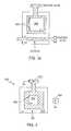
- FIGS. 1 a - 1 dAnti-fuses according to an embodiment of the present invention are shown in FIGS. 1 a - 1 d , wherein FIGS. 1 a and 1 b are cross-sectional and top views, respectively, of an n-type anti-fuse 100 , and FIGS. 1 c and 1 d are cross-sectional and top views, respectively, of a p-type anti-fuse 150 .
- Anti-fuses 100 , 150comprise heavily doped diffusions of the same type as the background; e.g., an n+ doped active region 105 in an n-well 110 of an n or p substrate 115 (or simply an n+ region in an n substrate), or a p+ doped active region 155 in a p-well 160 of an n or p substrate 165 (or simply a p+ region in a p substrate).
- a conductive gate 125 , 175such as polysilicon or polycide, is then formed, as by deposition, masking and etching of a layer of polysilicon, on gate oxide 120 , 170 .
- Gate 125 , 175preferably has a dimension (e.g., gate length) about equal to the minimum feature size according to the design rules of the semiconductor device, to minimize the program voltage necessary to blow anti-fuse 100 , 150 .
- a channel region 130 , 180is disposed adjacent to active region 105 , 155 under gate 125 , 175 .
- Field oxide regions 135 , 185such as silicon dioxide formed by deposition, are disposed adjacent to active region 105 , 155 and channel region 130 , 180 .
- inventive antifuse 100 , 150will look like half of a transistor from a topographical viewpoint. However, it will not be a transistor; it will be a capacitor, wherein channel 130 , 180 forms when a voltage is placed between gate 125 , 175 and heavily doped active region 105 , 155 .
- a portion of active region 105 , 155extends under an edge 125 a , 175 a of gate 125 , 175 .
- the simple capacitor anti-fuse 100 , 150 of this embodimentprovides high electric field strength, especially where the n+ or p+ diffusions of active region 105 , 155 extend under the edge 125 a , 175 a of gate 125 , 175 . Since gate/diffusion edge 125 a , 175 a is the most likely spot for the anti-fuse to program (i.e., for gate oxide 120 , 170 to be blown), it also will result in the least gate polysilicon/diffusion resistance once programmed.
- the actual gate oxide anti-fuseis the thin gate oxide portion 120 a , 170 a between the gate and the underlying diffusions.
- Anti-fuse 100 of FIGS. 1 a-bcan be programmed to n-well 110 , but because of the electric field strength, programming is most likely to occur into n-plus region 105 because of electric field fringing. The analogous situation will occur in anti-fuse 150 of FIGS. 1 c-d.
- the inventive anti-fuses such as anti-fuse 100are formed simultaneously with other devices on the substrate, such as transistors.
- gate oxide 120 of anti-fuse 100is formed at the same time and to the same thickness as the gate oxide for the remainder of the devices formed on substrate 115 .
- Gate 125 of anti-fuse 100is formed on gate oxide 120 at the same time as the gates for other devices formed on substrate 115 , but is typically has much smaller dimensions, as discussed above.
- active region 105is formed with the same ion implantation step used to form source/drain regions for other devices. Active region 105 is typically formed after gate 125 by ion implanting impurities using gate 125 as a mask, since this is how MOS transistors are typically formed.
- the inventive anti-fuseis formed without additional processing steps beyond those necessary to form the other MOS devices on the substrate.
- the inventive anti-fuseonly requires for its formation changing the patterning of the layers already being formed.
- gate oxide 120 , 170will begin to draw current at about 5 millivolts per centimeter. If gate oxide 120 , 170 is about 100 angstroms thick, tunneling begins about 6 millivolts per centimeters or 6 volts. Commonly, 30 angstrom gate oxides are employed, in which case tunnelling will begin to occur at about 1.8 volts to about 2 volts. Somewhere between 10 millivolts and 12 millivolts, the gate oxide will rapidly fail. Thus, rapid programming will occur between 12 and 15 millivolts, as high amounts of current flux causes gate oxide 120 , 170 to heat up, melt and finally fail.
- the breakdown voltageis raised by about 70% by connecting two MOS devices in a well-known cascode configuration and biasing the upper gate at about half the intended breakdown voltage. So, if gate diode breakdown voltage with a 50 ⁇ gate oxide results in a single transistor drain breakdown voltage of 5 volts @ 10 ⁇ V/cm, then a cascode can be expected to provide an 8.5V breakdown with the consequent capability of applying up to 17 ⁇ V/cm on a 50 ⁇ gate oxide anti-fuse. Moreover, as gate oxide is scaled below 50 ⁇ to, for example, about 25 ⁇ , the cascode breakdown voltage capability will scale with it. Furthermore, since the applied voltage on the driver transistor during the one-time programming is in the seconds to milliseconds range, transistor reliability hazard is only limited to this short duration of programming.
- FIGS. 2 a and 2 bProgram and read circuitry for the inventive anti-fuses is shown in FIGS. 2 a and 2 b , wherein a cascode technique is utilized to mitigate the stress on the driver transistors by enabling the programming voltage load to be applied to an anti-fuse 230 to be shared between two program cascode transistors 210 , 220 of a program cascode 200 , and to enable the programmed anti-fuse to be read by a read cascode 240 .
- a temporary high voltage power sourceis needed. This can be supplied externally, or with a conventional on-chip charge-pump and a storage capacitor (not shown) much larger than the anti-fuse being programmed.
- each program cascode transistor 210 , 220 of program cascode 200handles about 4.25 volts, or half the programming voltage (Vdd) of about 8.5 volts which is applied to anti-fuse 230 to program it.
- Read cascode 240is disabled by grounding control gates 250 a , 260 a of read cascode transistors 250 , 260 .
- control gate 210 a of top cascode transistor 210is applied to control gate 210 a of top cascode transistor 210 to turn it on (e.g., more than about 2 volts relative to its source 210 b , such as about 6.5 volts or less), while applying about 4.25 volts to control gate 220 a of bottom cascode transistor 220 .
- 8.5 voltsis applied to top cascode transistor 210 with its source 210 b grounded (i.e., tied to its gate 210 a ) to turn off transistor 210 .
- the read mode program cascode 200(also called a “write cascode”) is used to supply current to anti-fuse 230 and the resulting voltage V r (e.g., about 2 volts) is sensed by read cascode 240 . If anti-fuse 230 is open (i.e., it was never programmed), voltage V r will be high. However, if anti-fuse 230 is shorted (i.e., if it has been programmed), voltage V r will be low.
- V re.g., about 2 volts
- a sufficient voltage(e.g., about 2 volts) is applied to gate 250 a to turn on upper read cascode transistor 250 to place potential V r on a read node 270 between read cascode transistors 250 , 260 .
- This signalis then fed to logic circuitry (not shown), such as 2 volt logic circuits.
- An array of inventive anti-fuses(e.g. anti-fuse 200 , 100 or 150 ) can be provided on a substrate, each one having read and program circuitry as shown in FIGS. 2 a-b , typically with the read circuits tied together.
- program cascode 200all the read and program cascodes can be operated as shown in FIG. 2 b so that the data from all the read nodes on the array is fed into the 2 volt logic circuitry, enabling the data stored in the anti-fuses to be recovered.
- Transistorsare typically designed to minimize and mitigate peak electric fields on gate oxide using “channel engineering”.
- the reverse strategyis available for the thin oxide anti-fuse.
- a high voltage MOS cascode 300having transistors 310 , 320 as shown in FIG. 3 a .
- the cascode gateis enclosed in a “donut” to get rid of any parasitic field oxide transistor action.
- Such a gate arrangementis shown in FIG. 3 b .
- the sharp n+ drain corner electric fieldis mitigated and breakdown voltage is raised by typically about 10% in the device of FIG. 3 b vs.
- FIG. 3 cwhich has square corners 350 on its drain diffusion 360 .
- the thin gate oxide (not shown) of the transistorwill fail at a lower voltage than the gate oxide of the device of FIG. 3 b.
- the antifuse 400 of another embodiment of the present inventionshown in FIG. 4 .
- the gate oxide(not shown) can be easily blown with the breakdown voltage of cascode transistor 310 of FIG. 3 b to program the device.
- the ultra-small corners 440(e.g., effectively about 0.02 ⁇ 0.02 ⁇ each) provide an effective gate oxide area of 4 ⁇ (0.02 ⁇ 0.02 ⁇ ), or 0.0016 ⁇ 2 .
- the arrangement of FIG. 3 bmay also be done with p-channel transistors, thus providing a complementary set of driver transistors for anti-fuse transistor 400 .
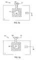
- FIG. 5 ashows an n+ gated diode/thin oxide anti-fuse 500
- FIG. 5 bshows a p+ gated diode/thin oxide anti-fuse 550 according to further embodiments of the present invention.
- Gated diode anti-fuses 500 , 500feature an active region field oxide edge 510 , 560 that allows active region 520 , 570 to partially extend under the donut hole of gate 530 , 580 .
- anti-fuse 610comprises an n+ drain region 611 and a p+ source region 612 formed in a p-well (or p substrate) 613 and separated by a channel region (not shown), and a gate 614 formed on the channel region.
- Gate 614 and source 612are both grounded.
- anti-fuse 620comprises a p+ drain region 621 and an n+ source region 622 formed in an n-well (or n substrate) 623 and separated by a channel region (not shown), and a gate 624 formed on the channel region. Gate 624 and source 622 are both grounded.
- anti-fuse 630comprises an n+ drain region 631 and a much smaller p+ source region 632 formed in a p-well (or p substrate) 633 , and a gate 634 formed above an edge of drain region 631 and above where it meets p-well 633 .
- Gate 634 and source 632are both grounded.
- anti-fuse 640comprises a p+ drain region 641 and a much smaller n+ source region 642 formed in an n-well (or n substrate) 643 , and a gate 644 formed above an edge of drain region 641 above where it meets n-well 643 .
- Gate 644 and source 642are both grounded.
- topographical geometriescan be used to form anti-fuses according to the present invention. Any poly/gate oxide/substrate (or well) combination can be used. Positive or negative polarities can be used for both programming and read functions. Step function programming pulses can be used or any type of voltage/current ramp/waveform programming can be used. Multiple pulse programming can also be used.
- the present inventionis applicable to the manufacture of various types of semiconductor devices, particularly high density semiconductor devices having a design rule of about 0.18 ⁇ and under.
Landscapes
- Physics & Mathematics (AREA)
- Condensed Matter Physics & Semiconductors (AREA)
- General Physics & Mathematics (AREA)
- Engineering & Computer Science (AREA)
- Computer Hardware Design (AREA)
- Microelectronics & Electronic Packaging (AREA)
- Power Engineering (AREA)
- Design And Manufacture Of Integrated Circuits (AREA)
Abstract
Description
Claims (8)
Priority Applications (1)
| Application Number | Priority Date | Filing Date | Title |
|---|---|---|---|
| US09/698,485US6515344B1 (en) | 1999-10-28 | 2000-10-30 | Thin oxide anti-fuse |
Applications Claiming Priority (2)
| Application Number | Priority Date | Filing Date | Title |
|---|---|---|---|
| US16191099P | 1999-10-28 | 1999-10-28 | |
| US09/698,485US6515344B1 (en) | 1999-10-28 | 2000-10-30 | Thin oxide anti-fuse |
Publications (1)
| Publication Number | Publication Date |
|---|---|
| US6515344B1true US6515344B1 (en) | 2003-02-04 |
Family
ID=26858252
Family Applications (1)
| Application Number | Title | Priority Date | Filing Date |
|---|---|---|---|
| US09/698,485Expired - LifetimeUS6515344B1 (en) | 1999-10-28 | 2000-10-30 | Thin oxide anti-fuse |
Country Status (1)
| Country | Link |
|---|---|
| US (1) | US6515344B1 (en) |
Cited By (35)
| Publication number | Priority date | Publication date | Assignee | Title |
|---|---|---|---|---|
| US20030115191A1 (en)* | 2001-12-17 | 2003-06-19 | Max Copperman | Efficient and cost-effective content provider for customer relationship management (CRM) or other applications |
| US20040065941A1 (en)* | 2000-08-31 | 2004-04-08 | Micron Technology, Inc. | Gate dielectric antifuse circuits and methods for operating same |
| US20040155315A1 (en)* | 2002-08-29 | 2004-08-12 | Micron Technology, Inc. | Circuits and methods to protect a gate dielectric antifuse |
| US20040212037A1 (en)* | 2000-12-20 | 2004-10-28 | Broadcom Corporation | System and method for one-time programmed memory through direct-tunneling oxide breakdown |
| US20040219760A1 (en)* | 2002-08-29 | 2004-11-04 | Micro Technology, Inc. | Cascode I/O driver with improved ESD operation |
| US20060067152A1 (en)* | 2004-09-29 | 2006-03-30 | Ali Keshavarzi | Crosspoint memory array utilizing one time programmable antifuse cells |
| US20060092742A1 (en)* | 2004-11-01 | 2006-05-04 | Fabrice Paillet | OTP antifuse cell and cell array |
| US20060226509A1 (en)* | 2005-03-31 | 2006-10-12 | Min Won G | Antifuse element and electrically redundant antifuse array for controlled rupture location |
| US20060231922A1 (en)* | 2002-08-29 | 2006-10-19 | Micron Technology, Inc. | Gate dielectric antifuse circuit to protect a high-voltage transistor |
| US20060244099A1 (en)* | 2004-05-06 | 2006-11-02 | Wlodek Kurjanowicz | Split-channel antifuse array architecture |
| US20060258140A1 (en)* | 2003-10-23 | 2006-11-16 | Armin Fischer | Integrated circuit with additional mini-pads connected by an under-bump metallization and method for production thereof |
| US20060285393A1 (en)* | 2005-06-21 | 2006-12-21 | Fabrice Paillet | Apparatus and method for programming a memory array |
| US20060292755A1 (en)* | 2005-06-28 | 2006-12-28 | Parris Patrice M | Tunable antifuse element and method of manufacture |
| US20060291265A1 (en)* | 2005-06-27 | 2006-12-28 | Gerhard Schrom | Memory cell driver circuits |
| US20070030719A1 (en)* | 2005-08-05 | 2007-02-08 | Hoefler Alexander B | One time programmable memory and method of operation |
| US20070165441A1 (en)* | 2004-05-06 | 2007-07-19 | Sidense Corporation | High speed otp sensing scheme |
| US20070247902A1 (en)* | 2006-04-20 | 2007-10-25 | Hsin-Ming Chen | Method for operating a single-poly single-transistor non-volatile memory cell |
| US20070257331A1 (en)* | 2004-05-06 | 2007-11-08 | Sidense Corporation | Anti-fuse memory cell |
| US7312513B1 (en)* | 2006-07-10 | 2007-12-25 | Wilcox William J | Antifuse circuit with well bias transistor |
| US7321502B2 (en) | 2004-09-30 | 2008-01-22 | Intel Corporation | Non volatile data storage through dielectric breakdown |
| US20080036033A1 (en)* | 2006-08-10 | 2008-02-14 | Broadcom Corporation | One-time programmable memory |
| US20080085574A1 (en)* | 2006-10-05 | 2008-04-10 | Hoefler Alexander B | Antifuse one time programmable memory array and method of manufacture |
| US20090026576A1 (en)* | 2007-07-24 | 2009-01-29 | United Microelectronics Corp. | Anti-fuse |
| US20090096501A1 (en)* | 2007-10-10 | 2009-04-16 | Atmel Corporation | Apparatus and method for preventing snap back in integrated circuits |
| US20090189248A1 (en)* | 2008-01-30 | 2009-07-30 | Elpida Memory, Inc. | Semiconductor device and method of manufacturing the same |
| US20100086153A1 (en)* | 1997-01-13 | 2010-04-08 | Micro Ear Technology, Inc. D/B/A Micro-Tech | Portable system for programming hearing aids |
| US20100149710A1 (en)* | 2008-12-12 | 2010-06-17 | Atmel Corporation | Snap-back tolerant integrated circuits |
| US8350264B2 (en) | 2010-07-14 | 2013-01-08 | International Businesss Machines Corporation | Secure anti-fuse with low voltage programming through localized diffusion heating |
| US8735297B2 (en) | 2004-05-06 | 2014-05-27 | Sidense Corporation | Reverse optical proximity correction method |
| US8767433B2 (en) | 2004-05-06 | 2014-07-01 | Sidense Corp. | Methods for testing unprogrammed OTP memory |
| US9123572B2 (en) | 2004-05-06 | 2015-09-01 | Sidense Corporation | Anti-fuse memory cell |
| US20160300622A1 (en)* | 2015-04-12 | 2016-10-13 | NEO Semiconductor, Inc. | CMOS Anti-Fuse Cell |
| US9761595B2 (en)* | 2013-02-21 | 2017-09-12 | Infineon Technologies Ag | One-time programming device and a semiconductor device |
| CN114078859A (en)* | 2020-08-10 | 2022-02-22 | 南亚科技股份有限公司 | Programmable memory element |
| TWI786759B (en)* | 2020-08-18 | 2022-12-11 | 南亞科技股份有限公司 | Antifuse structure |
Citations (9)
| Publication number | Priority date | Publication date | Assignee | Title |
|---|---|---|---|---|
| US4543594A (en)* | 1982-09-07 | 1985-09-24 | Intel Corporation | Fusible link employing capacitor structure |
| US4562639A (en)* | 1982-03-23 | 1986-01-07 | Texas Instruments Incorporated | Process for making avalanche fuse element with isolated emitter |
| US4881114A (en)* | 1986-05-16 | 1989-11-14 | Actel Corporation | Selectively formable vertical diode circuit element |
| US4943538A (en)* | 1986-05-09 | 1990-07-24 | Actel Corporation | Programmable low impedance anti-fuse element |
| US5057451A (en)* | 1990-04-12 | 1991-10-15 | Actel Corporation | Method of forming an antifuse element with substantially reduced capacitance using the locos technique |
| US5110754A (en)* | 1991-10-04 | 1992-05-05 | Micron Technology, Inc. | Method of making a DRAM capacitor for use as an programmable antifuse for redundancy repair/options on a DRAM |
| EP0495317A1 (en)* | 1991-01-18 | 1992-07-22 | Actel Corporation | Low voltage programmable antifuse and method for programming same |
| US5635873A (en)* | 1992-04-27 | 1997-06-03 | Dallas Semiconductor Corp. | Operational amplifier having dummy isolation stage |
| US5742555A (en)* | 1996-08-20 | 1998-04-21 | Micron Technology, Inc. | Method of anti-fuse repair |
- 2000
- 2000-10-30USUS09/698,485patent/US6515344B1/ennot_activeExpired - Lifetime
Patent Citations (9)
| Publication number | Priority date | Publication date | Assignee | Title |
|---|---|---|---|---|
| US4562639A (en)* | 1982-03-23 | 1986-01-07 | Texas Instruments Incorporated | Process for making avalanche fuse element with isolated emitter |
| US4543594A (en)* | 1982-09-07 | 1985-09-24 | Intel Corporation | Fusible link employing capacitor structure |
| US4943538A (en)* | 1986-05-09 | 1990-07-24 | Actel Corporation | Programmable low impedance anti-fuse element |
| US4881114A (en)* | 1986-05-16 | 1989-11-14 | Actel Corporation | Selectively formable vertical diode circuit element |
| US5057451A (en)* | 1990-04-12 | 1991-10-15 | Actel Corporation | Method of forming an antifuse element with substantially reduced capacitance using the locos technique |
| EP0495317A1 (en)* | 1991-01-18 | 1992-07-22 | Actel Corporation | Low voltage programmable antifuse and method for programming same |
| US5110754A (en)* | 1991-10-04 | 1992-05-05 | Micron Technology, Inc. | Method of making a DRAM capacitor for use as an programmable antifuse for redundancy repair/options on a DRAM |
| US5635873A (en)* | 1992-04-27 | 1997-06-03 | Dallas Semiconductor Corp. | Operational amplifier having dummy isolation stage |
| US5742555A (en)* | 1996-08-20 | 1998-04-21 | Micron Technology, Inc. | Method of anti-fuse repair |
Cited By (82)
| Publication number | Priority date | Publication date | Assignee | Title |
|---|---|---|---|---|
| US20100086153A1 (en)* | 1997-01-13 | 2010-04-08 | Micro Ear Technology, Inc. D/B/A Micro-Tech | Portable system for programming hearing aids |
| US7030458B2 (en)* | 2000-08-31 | 2006-04-18 | Micron Technology, Inc. | Gate dielectric antifuse circuits and methods for operating same |
| US20040065941A1 (en)* | 2000-08-31 | 2004-04-08 | Micron Technology, Inc. | Gate dielectric antifuse circuits and methods for operating same |
| US20060097345A1 (en)* | 2000-08-31 | 2006-05-11 | Micron Technology, Inc. | Gate dielectric antifuse circuits and methods for operating same |
| US20040212037A1 (en)* | 2000-12-20 | 2004-10-28 | Broadcom Corporation | System and method for one-time programmed memory through direct-tunneling oxide breakdown |
| US20050219889A1 (en)* | 2000-12-20 | 2005-10-06 | Broadcom Corporation | System and method for one-time programmed memory through direct-tunneling oxide breakdown |
| US6960819B2 (en) | 2000-12-20 | 2005-11-01 | Broadcom Corporation | System and method for one-time programmed memory through direct-tunneling oxide breakdown |
| US7009891B2 (en) | 2000-12-20 | 2006-03-07 | Broadcom Corporation | System and method for one-time programmed memory through direct-tunneling oxide breakdown |
| US20030115191A1 (en)* | 2001-12-17 | 2003-06-19 | Max Copperman | Efficient and cost-effective content provider for customer relationship management (CRM) or other applications |
| US7903379B2 (en) | 2002-08-29 | 2011-03-08 | Micron Technology, Inc. | Cascode I/O driver with improved ESD operation |
| US20040219760A1 (en)* | 2002-08-29 | 2004-11-04 | Micro Technology, Inc. | Cascode I/O driver with improved ESD operation |
| US20040155315A1 (en)* | 2002-08-29 | 2004-08-12 | Micron Technology, Inc. | Circuits and methods to protect a gate dielectric antifuse |
| US7405463B2 (en) | 2002-08-29 | 2008-07-29 | Micron Technology, Inc. | Gate dielectric antifuse circuit to protect a high-voltage transistor |
| US20060231922A1 (en)* | 2002-08-29 | 2006-10-19 | Micron Technology, Inc. | Gate dielectric antifuse circuit to protect a high-voltage transistor |
| US7126871B2 (en) | 2002-08-29 | 2006-10-24 | Micron Technology, Inc. | Circuits and methods to protect a gate dielectric antifuse |
| US20080019064A1 (en)* | 2002-08-29 | 2008-01-24 | Micron Technology, Inc. | Cascode i/o driver with improved esd operation |
| US7253064B2 (en)* | 2002-08-29 | 2007-08-07 | Micron Technology, Inc. | Cascode I/O driver with improved ESD operation |
| US7919363B2 (en)* | 2003-10-23 | 2011-04-05 | Infineon Technologies Ag | Integrated circuit with additional mini-pads connected by an under-bump metallization and method for production thereof |
| US20110140236A1 (en)* | 2003-10-23 | 2011-06-16 | Armin Fischer | Integrated Circuit with Pads Connected by an Under-Bump Metallization and Method for Production Thereof |
| US20060258140A1 (en)* | 2003-10-23 | 2006-11-16 | Armin Fischer | Integrated circuit with additional mini-pads connected by an under-bump metallization and method for production thereof |
| US8487453B2 (en) | 2003-10-23 | 2013-07-16 | Infineon Technologies Ag | Integrated circuit with pads connected by an under-bump metallization and method for production thereof |
| US20080038879A1 (en)* | 2004-05-06 | 2008-02-14 | Sidense Corporation | Split-channel antifuse array architecture |
| US20070257331A1 (en)* | 2004-05-06 | 2007-11-08 | Sidense Corporation | Anti-fuse memory cell |
| US8767433B2 (en) | 2004-05-06 | 2014-07-01 | Sidense Corp. | Methods for testing unprogrammed OTP memory |
| US8735297B2 (en) | 2004-05-06 | 2014-05-27 | Sidense Corporation | Reverse optical proximity correction method |
| US9123572B2 (en) | 2004-05-06 | 2015-09-01 | Sidense Corporation | Anti-fuse memory cell |
| US20070165441A1 (en)* | 2004-05-06 | 2007-07-19 | Sidense Corporation | High speed otp sensing scheme |
| US20090154217A1 (en)* | 2004-05-06 | 2009-06-18 | Sidense Corp. | High speed otp sensing scheme |
| US7755162B2 (en) | 2004-05-06 | 2010-07-13 | Sidense Corp. | Anti-fuse memory cell |
| US8313987B2 (en)* | 2004-05-06 | 2012-11-20 | Sidense Corp. | Anti-fuse memory cell |
| US7511982B2 (en) | 2004-05-06 | 2009-03-31 | Sidense Corp. | High speed OTP sensing scheme |
| US8283751B2 (en) | 2004-05-06 | 2012-10-09 | Sidense Corp. | Split-channel antifuse array architecture |
| US8130532B2 (en) | 2004-05-06 | 2012-03-06 | Sidense Corp. | High speed OTP sensing scheme |
| US7764532B2 (en) | 2004-05-06 | 2010-07-27 | Sidense Corp. | High speed OTP sensing scheme |
| US20060244099A1 (en)* | 2004-05-06 | 2006-11-02 | Wlodek Kurjanowicz | Split-channel antifuse array architecture |
| US20110312169A1 (en)* | 2004-05-06 | 2011-12-22 | Sidense Corp. | Anti-fuse memory cell |
| US7642138B2 (en) | 2004-05-06 | 2010-01-05 | Sidense Corporation | Split-channel antifuse array architecture |
| US8026574B2 (en) | 2004-05-06 | 2011-09-27 | Sidense Corporation | Anti-fuse memory cell |
| US7402855B2 (en) | 2004-05-06 | 2008-07-22 | Sidense Corp. | Split-channel antifuse array architecture |
| US20100259965A1 (en)* | 2004-05-06 | 2010-10-14 | Sidense Corp. | High speed otp sensing scheme |
| US7110278B2 (en) | 2004-09-29 | 2006-09-19 | Intel Corporation | Crosspoint memory array utilizing one time programmable antifuse cells |
| US20060067152A1 (en)* | 2004-09-29 | 2006-03-30 | Ali Keshavarzi | Crosspoint memory array utilizing one time programmable antifuse cells |
| US7321502B2 (en) | 2004-09-30 | 2008-01-22 | Intel Corporation | Non volatile data storage through dielectric breakdown |
| US7102951B2 (en) | 2004-11-01 | 2006-09-05 | Intel Corporation | OTP antifuse cell and cell array |
| US20060092742A1 (en)* | 2004-11-01 | 2006-05-04 | Fabrice Paillet | OTP antifuse cell and cell array |
| US20060226509A1 (en)* | 2005-03-31 | 2006-10-12 | Min Won G | Antifuse element and electrically redundant antifuse array for controlled rupture location |
| US7256471B2 (en)* | 2005-03-31 | 2007-08-14 | Freescale Semiconductor, Inc. | Antifuse element and electrically redundant antifuse array for controlled rupture location |
| US7167397B2 (en)* | 2005-06-21 | 2007-01-23 | Intel Corporation | Apparatus and method for programming a memory array |
| US20060285393A1 (en)* | 2005-06-21 | 2006-12-21 | Fabrice Paillet | Apparatus and method for programming a memory array |
| US20060291265A1 (en)* | 2005-06-27 | 2006-12-28 | Gerhard Schrom | Memory cell driver circuits |
| US7236410B2 (en) | 2005-06-27 | 2007-06-26 | Intel Corporation | Memory cell driver circuits |
| US20090127587A1 (en)* | 2005-06-28 | 2009-05-21 | Freescale Semiconductor, Inc. | Tunable antifuse elements |
| US20060292755A1 (en)* | 2005-06-28 | 2006-12-28 | Parris Patrice M | Tunable antifuse element and method of manufacture |
| US7528015B2 (en) | 2005-06-28 | 2009-05-05 | Freescale Semiconductor, Inc. | Tunable antifuse element and method of manufacture |
| US7700996B2 (en) | 2005-06-28 | 2010-04-20 | Freescale Semiconductor, Inc. | Tunable antifuse elements |
| US7206214B2 (en) | 2005-08-05 | 2007-04-17 | Freescale Semiconductor, Inc. | One time programmable memory and method of operation |
| US20070030719A1 (en)* | 2005-08-05 | 2007-02-08 | Hoefler Alexander B | One time programmable memory and method of operation |
| US7417897B2 (en)* | 2006-04-20 | 2008-08-26 | Ememory Technology Inc. | Method for reading a single-poly single-transistor non-volatile memory cell |
| US20070247902A1 (en)* | 2006-04-20 | 2007-10-25 | Hsin-Ming Chen | Method for operating a single-poly single-transistor non-volatile memory cell |
| US7312513B1 (en)* | 2006-07-10 | 2007-12-25 | Wilcox William J | Antifuse circuit with well bias transistor |
| US7977765B2 (en) | 2006-07-10 | 2011-07-12 | Micron Technology, Inc. | Antifuse circuit with well bias transistor |
| US20100135096A1 (en)* | 2006-07-10 | 2010-06-03 | Micron Technology, Inc. | Antifuse circuit with well bias transistor |
| US20080007985A1 (en)* | 2006-07-10 | 2008-01-10 | Wilcox William J | Antifuse circuit with well bias transistor |
| US20080036033A1 (en)* | 2006-08-10 | 2008-02-14 | Broadcom Corporation | One-time programmable memory |
| US7678620B2 (en) | 2006-10-05 | 2010-03-16 | Freescale Semiconductor, Inc. | Antifuse one time programmable memory array and method of manufacture |
| US20080085574A1 (en)* | 2006-10-05 | 2008-04-10 | Hoefler Alexander B | Antifuse one time programmable memory array and method of manufacture |
| WO2008151429A1 (en) | 2007-06-13 | 2008-12-18 | Sidense Corp. | Anti-fuse memory cell |
| US20090026576A1 (en)* | 2007-07-24 | 2009-01-29 | United Microelectronics Corp. | Anti-fuse |
| US20090096501A1 (en)* | 2007-10-10 | 2009-04-16 | Atmel Corporation | Apparatus and method for preventing snap back in integrated circuits |
| US7692483B2 (en) | 2007-10-10 | 2010-04-06 | Atmel Corporation | Apparatus and method for preventing snap back in integrated circuits |
| US8729642B2 (en) | 2008-01-30 | 2014-05-20 | Eiji Kitamura | Semiconductor device comprising a gate electrode having an opening |
| US20090189248A1 (en)* | 2008-01-30 | 2009-07-30 | Elpida Memory, Inc. | Semiconductor device and method of manufacturing the same |
| JP2009206490A (en)* | 2008-01-30 | 2009-09-10 | Elpida Memory Inc | Semiconductor device and method of manufacturing the same |
| US20100149710A1 (en)* | 2008-12-12 | 2010-06-17 | Atmel Corporation | Snap-back tolerant integrated circuits |
| US8085604B2 (en) | 2008-12-12 | 2011-12-27 | Atmel Corporation | Snap-back tolerant integrated circuits |
| US8569755B2 (en) | 2010-07-14 | 2013-10-29 | International Business Machines Corporation | Secure anti-fuse with low voltage programming through localized diffusion heating |
| US8350264B2 (en) | 2010-07-14 | 2013-01-08 | International Businesss Machines Corporation | Secure anti-fuse with low voltage programming through localized diffusion heating |
| US9761595B2 (en)* | 2013-02-21 | 2017-09-12 | Infineon Technologies Ag | One-time programming device and a semiconductor device |
| US20160300622A1 (en)* | 2015-04-12 | 2016-10-13 | NEO Semiconductor, Inc. | CMOS Anti-Fuse Cell |
| US9793001B2 (en)* | 2015-04-12 | 2017-10-17 | NEO Semiconductor, Inc. | CMOS anti-fuse cell |
| CN114078859A (en)* | 2020-08-10 | 2022-02-22 | 南亚科技股份有限公司 | Programmable memory element |
| TWI786759B (en)* | 2020-08-18 | 2022-12-11 | 南亞科技股份有限公司 | Antifuse structure |
Similar Documents
| Publication | Publication Date | Title |
|---|---|---|
| US6515344B1 (en) | Thin oxide anti-fuse | |
| US7102951B2 (en) | OTP antifuse cell and cell array | |
| JP5204125B2 (en) | High-speed OTP sensing scheme | |
| US6642601B2 (en) | Low current substantially silicide fuse for integrated circuits | |
| JP4981661B2 (en) | Split channel antifuse array structure | |
| US6909635B2 (en) | Programmable memory cell using charge trapping in a gate oxide | |
| US6992925B2 (en) | High density semiconductor memory cell and memory array using a single transistor and having counter-doped poly and buried diffusion wordline | |
| US5646438A (en) | Programmable semiconductor memory | |
| US6498739B2 (en) | Applications for non-volatile memory cells | |
| US7531886B2 (en) | MOSFET fuse programmed by electromigration | |
| US7724572B2 (en) | Integrated circuit having a non-volatile memory cell transistor as a fuse device | |
| EP1329901B1 (en) | Memory cell with fuse element | |
| US6617637B1 (en) | Electrically erasable programmable logic device | |
| KR100712089B1 (en) | Semiconductor memory device and manufacturing method | |
| US20120039106A1 (en) | Programmable Memory Cell with Shiftable Threshold Voltage Transistor | |
| US6693481B1 (en) | Fuse circuit utilizing high voltage transistors | |
| US7564707B2 (en) | One-time programmable non-volatile memory | |
| US7075127B2 (en) | Single-poly 2-transistor based fuse element | |
| US7110278B2 (en) | Crosspoint memory array utilizing one time programmable antifuse cells | |
| US7126204B2 (en) | Integrated semiconductor circuit with an electrically programmable switching element | |
| US6445041B1 (en) | Semiconductor memory cell array with reduced parasitic capacitance between word lines and bit lines | |
| US6020777A (en) | Electrically programmable anti-fuse circuit | |
| US6535046B2 (en) | Integrated semiconductor circuit with an increased operating voltage | |
| US5841723A (en) | Method and apparatus for programming anti-fuses using an isolated well programming circuit | |
| US6472275B2 (en) | Read-only memory and method for fabricating the same |
Legal Events
| Date | Code | Title | Description |
|---|---|---|---|
| AS | Assignment | Owner name:ADVANCED MICRO DEVICES, INC., CALIFORNIA Free format text:ASSIGNMENT OF ASSIGNORS INTEREST;ASSIGNOR:WOLLESEN, DONALD L.;REEL/FRAME:011525/0395 Effective date:20010131 | |
| STCF | Information on status: patent grant | Free format text:PATENTED CASE | |
| FPAY | Fee payment | Year of fee payment:4 | |
| AS | Assignment | Owner name:SPANSION INC., CALIFORNIA Free format text:ASSIGNMENT OF ASSIGNORS INTEREST;ASSIGNOR:ADVANCED MICRO DEVICES, INC.;REEL/FRAME:019028/0674 Effective date:20070131 | |
| AS | Assignment | Owner name:SPANSION LLC, CALIFORNIA Free format text:ASSIGNMENT OF ASSIGNORS INTEREST;ASSIGNOR:SPANSION INC.;REEL/FRAME:019069/0131 Effective date:20070131 | |
| AS | Assignment | Owner name:BARCLAYS BANK PLC,NEW YORK Free format text:SECURITY AGREEMENT;ASSIGNORS:SPANSION LLC;SPANSION INC.;SPANSION TECHNOLOGY INC.;AND OTHERS;REEL/FRAME:024522/0338 Effective date:20100510 Owner name:BARCLAYS BANK PLC, NEW YORK Free format text:SECURITY AGREEMENT;ASSIGNORS:SPANSION LLC;SPANSION INC.;SPANSION TECHNOLOGY INC.;AND OTHERS;REEL/FRAME:024522/0338 Effective date:20100510 | |
| FPAY | Fee payment | Year of fee payment:8 | |
| FPAY | Fee payment | Year of fee payment:12 | |
| AS | Assignment | Owner name:SPANSION LLC, CALIFORNIA Free format text:RELEASE BY SECURED PARTY;ASSIGNOR:BARCLAYS BANK PLC;REEL/FRAME:035201/0159 Effective date:20150312 Owner name:SPANSION TECHNOLOGY LLC, CALIFORNIA Free format text:RELEASE BY SECURED PARTY;ASSIGNOR:BARCLAYS BANK PLC;REEL/FRAME:035201/0159 Effective date:20150312 Owner name:SPANSION INC., CALIFORNIA Free format text:RELEASE BY SECURED PARTY;ASSIGNOR:BARCLAYS BANK PLC;REEL/FRAME:035201/0159 Effective date:20150312 | |
| AS | Assignment | Owner name:MORGAN STANLEY SENIOR FUNDING, INC., NEW YORK Free format text:SECURITY INTEREST;ASSIGNORS:CYPRESS SEMICONDUCTOR CORPORATION;SPANSION LLC;REEL/FRAME:035240/0429 Effective date:20150312 | |
| AS | Assignment | Owner name:CYPRESS SEMICONDUCTOR CORPORATION, CALIFORNIA Free format text:ASSIGNMENT OF ASSIGNORS INTEREST;ASSIGNOR:SPANSION, LLC;REEL/FRAME:036025/0453 Effective date:20150601 | |
| AS | Assignment | Owner name:SPANSION LLC, CALIFORNIA Free format text:PARTIAL RELEASE OF SECURITY INTEREST IN PATENTS;ASSIGNOR:MORGAN STANLEY SENIOR FUNDING, INC., AS COLLATERAL AGENT;REEL/FRAME:039708/0001 Effective date:20160811 Owner name:CYPRESS SEMICONDUCTOR CORPORATION, CALIFORNIA Free format text:PARTIAL RELEASE OF SECURITY INTEREST IN PATENTS;ASSIGNOR:MORGAN STANLEY SENIOR FUNDING, INC., AS COLLATERAL AGENT;REEL/FRAME:039708/0001 Effective date:20160811 | |
| AS | Assignment | Owner name:MONTEREY RESEARCH, LLC, CALIFORNIA Free format text:ASSIGNMENT OF ASSIGNORS INTEREST;ASSIGNOR:CYPRESS SEMICONDUCTOR CORPORATION;REEL/FRAME:040911/0238 Effective date:20160811 | |
| AS | Assignment | Owner name:MORGAN STANLEY SENIOR FUNDING, INC., NEW YORK Free format text:CORRECTIVE ASSIGNMENT TO CORRECT THE 8647899 PREVIOUSLY RECORDED ON REEL 035240 FRAME 0429. ASSIGNOR(S) HEREBY CONFIRMS THE SECURITY INTERST;ASSIGNORS:CYPRESS SEMICONDUCTOR CORPORATION;SPANSION LLC;REEL/FRAME:058002/0470 Effective date:20150312 |