US6515300B2 - Method of making a TFT array with photo-imageable insulating layer over address lines - Google Patents
Method of making a TFT array with photo-imageable insulating layer over address linesDownload PDFInfo
- Publication number
- US6515300B2 US6515300B2US09/781,397US78139701AUS6515300B2US 6515300 B2US6515300 B2US 6515300B2US 78139701 AUS78139701 AUS 78139701AUS 6515300 B2US6515300 B2US 6515300B2
- Authority
- US
- United States
- Prior art keywords
- layer
- pixel
- insulating layer
- liquid crystal
- crystal display
- Prior art date
- Legal status (The legal status is an assumption and is not a legal conclusion. Google has not performed a legal analysis and makes no representation as to the accuracy of the status listed.)
- Expired - Lifetime
Links
Images


Classifications
- H—ELECTRICITY
- H10—SEMICONDUCTOR DEVICES; ELECTRIC SOLID-STATE DEVICES NOT OTHERWISE PROVIDED FOR
- H10F—INORGANIC SEMICONDUCTOR DEVICES SENSITIVE TO INFRARED RADIATION, LIGHT, ELECTROMAGNETIC RADIATION OF SHORTER WAVELENGTH OR CORPUSCULAR RADIATION
- H10F39/00—Integrated devices, or assemblies of multiple devices, comprising at least one element covered by group H10F30/00, e.g. radiation detectors comprising photodiode arrays
- H10F39/80—Constructional details of image sensors
- H10F39/802—Geometry or disposition of elements in pixels, e.g. address-lines or gate electrodes
- G—PHYSICS
- G02—OPTICS
- G02F—OPTICAL DEVICES OR ARRANGEMENTS FOR THE CONTROL OF LIGHT BY MODIFICATION OF THE OPTICAL PROPERTIES OF THE MEDIA OF THE ELEMENTS INVOLVED THEREIN; NON-LINEAR OPTICS; FREQUENCY-CHANGING OF LIGHT; OPTICAL LOGIC ELEMENTS; OPTICAL ANALOGUE/DIGITAL CONVERTERS
- G02F1/00—Devices or arrangements for the control of the intensity, colour, phase, polarisation or direction of light arriving from an independent light source, e.g. switching, gating or modulating; Non-linear optics
- G02F1/01—Devices or arrangements for the control of the intensity, colour, phase, polarisation or direction of light arriving from an independent light source, e.g. switching, gating or modulating; Non-linear optics for the control of the intensity, phase, polarisation or colour
- G02F1/13—Devices or arrangements for the control of the intensity, colour, phase, polarisation or direction of light arriving from an independent light source, e.g. switching, gating or modulating; Non-linear optics for the control of the intensity, phase, polarisation or colour based on liquid crystals, e.g. single liquid crystal display cells
- G02F1/133—Constructional arrangements; Operation of liquid crystal cells; Circuit arrangements
- G02F1/136—Liquid crystal cells structurally associated with a semi-conducting layer or substrate, e.g. cells forming part of an integrated circuit
- G02F1/1362—Active matrix addressed cells
- G02F1/136213—Storage capacitors associated with the pixel electrode
- G—PHYSICS
- G02—OPTICS
- G02F—OPTICAL DEVICES OR ARRANGEMENTS FOR THE CONTROL OF LIGHT BY MODIFICATION OF THE OPTICAL PROPERTIES OF THE MEDIA OF THE ELEMENTS INVOLVED THEREIN; NON-LINEAR OPTICS; FREQUENCY-CHANGING OF LIGHT; OPTICAL LOGIC ELEMENTS; OPTICAL ANALOGUE/DIGITAL CONVERTERS
- G02F1/00—Devices or arrangements for the control of the intensity, colour, phase, polarisation or direction of light arriving from an independent light source, e.g. switching, gating or modulating; Non-linear optics
- G02F1/01—Devices or arrangements for the control of the intensity, colour, phase, polarisation or direction of light arriving from an independent light source, e.g. switching, gating or modulating; Non-linear optics for the control of the intensity, phase, polarisation or colour
- G02F1/13—Devices or arrangements for the control of the intensity, colour, phase, polarisation or direction of light arriving from an independent light source, e.g. switching, gating or modulating; Non-linear optics for the control of the intensity, phase, polarisation or colour based on liquid crystals, e.g. single liquid crystal display cells
- G02F1/133—Constructional arrangements; Operation of liquid crystal cells; Circuit arrangements
- G02F1/136—Liquid crystal cells structurally associated with a semi-conducting layer or substrate, e.g. cells forming part of an integrated circuit
- G02F1/1362—Active matrix addressed cells
- G02F1/136227—Through-hole connection of the pixel electrode to the active element through an insulation layer
- G—PHYSICS
- G02—OPTICS
- G02F—OPTICAL DEVICES OR ARRANGEMENTS FOR THE CONTROL OF LIGHT BY MODIFICATION OF THE OPTICAL PROPERTIES OF THE MEDIA OF THE ELEMENTS INVOLVED THEREIN; NON-LINEAR OPTICS; FREQUENCY-CHANGING OF LIGHT; OPTICAL LOGIC ELEMENTS; OPTICAL ANALOGUE/DIGITAL CONVERTERS
- G02F1/00—Devices or arrangements for the control of the intensity, colour, phase, polarisation or direction of light arriving from an independent light source, e.g. switching, gating or modulating; Non-linear optics
- G02F1/01—Devices or arrangements for the control of the intensity, colour, phase, polarisation or direction of light arriving from an independent light source, e.g. switching, gating or modulating; Non-linear optics for the control of the intensity, phase, polarisation or colour
- G02F1/13—Devices or arrangements for the control of the intensity, colour, phase, polarisation or direction of light arriving from an independent light source, e.g. switching, gating or modulating; Non-linear optics for the control of the intensity, phase, polarisation or colour based on liquid crystals, e.g. single liquid crystal display cells
- G02F1/133—Constructional arrangements; Operation of liquid crystal cells; Circuit arrangements
- G02F1/136—Liquid crystal cells structurally associated with a semi-conducting layer or substrate, e.g. cells forming part of an integrated circuit
- G02F1/1362—Active matrix addressed cells
- G02F1/136286—Wiring, e.g. gate line, drain line
- H—ELECTRICITY
- H10—SEMICONDUCTOR DEVICES; ELECTRIC SOLID-STATE DEVICES NOT OTHERWISE PROVIDED FOR
- H10D—INORGANIC ELECTRIC SEMICONDUCTOR DEVICES
- H10D30/00—Field-effect transistors [FET]
- H10D30/01—Manufacture or treatment
- H10D30/021—Manufacture or treatment of FETs having insulated gates [IGFET]
- H10D30/031—Manufacture or treatment of FETs having insulated gates [IGFET] of thin-film transistors [TFT]
- H10D30/0312—Manufacture or treatment of FETs having insulated gates [IGFET] of thin-film transistors [TFT] characterised by the gate electrodes
- H10D30/0316—Manufacture or treatment of FETs having insulated gates [IGFET] of thin-film transistors [TFT] characterised by the gate electrodes of lateral bottom-gate TFTs comprising only a single gate
- H—ELECTRICITY
- H10—SEMICONDUCTOR DEVICES; ELECTRIC SOLID-STATE DEVICES NOT OTHERWISE PROVIDED FOR
- H10D—INORGANIC ELECTRIC SEMICONDUCTOR DEVICES
- H10D30/00—Field-effect transistors [FET]
- H10D30/01—Manufacture or treatment
- H10D30/021—Manufacture or treatment of FETs having insulated gates [IGFET]
- H10D30/031—Manufacture or treatment of FETs having insulated gates [IGFET] of thin-film transistors [TFT]
- H10D30/0321—Manufacture or treatment of FETs having insulated gates [IGFET] of thin-film transistors [TFT] comprising silicon, e.g. amorphous silicon or polysilicon
- H—ELECTRICITY
- H10—SEMICONDUCTOR DEVICES; ELECTRIC SOLID-STATE DEVICES NOT OTHERWISE PROVIDED FOR
- H10D—INORGANIC ELECTRIC SEMICONDUCTOR DEVICES
- H10D30/00—Field-effect transistors [FET]
- H10D30/60—Insulated-gate field-effect transistors [IGFET]
- H10D30/67—Thin-film transistors [TFT]
- H10D30/6704—Thin-film transistors [TFT] having supplementary regions or layers in the thin films or in the insulated bulk substrates for controlling properties of the device
- H10D30/6725—Thin-film transistors [TFT] having supplementary regions or layers in the thin films or in the insulated bulk substrates for controlling properties of the device having supplementary regions or layers for improving the flatness of the device
- H—ELECTRICITY
- H10—SEMICONDUCTOR DEVICES; ELECTRIC SOLID-STATE DEVICES NOT OTHERWISE PROVIDED FOR
- H10D—INORGANIC ELECTRIC SEMICONDUCTOR DEVICES
- H10D86/00—Integrated devices formed in or on insulating or conducting substrates, e.g. formed in silicon-on-insulator [SOI] substrates or on stainless steel or glass substrates
- H10D86/40—Integrated devices formed in or on insulating or conducting substrates, e.g. formed in silicon-on-insulator [SOI] substrates or on stainless steel or glass substrates characterised by multiple TFTs
- H10D86/441—Interconnections, e.g. scanning lines
- H—ELECTRICITY
- H10—SEMICONDUCTOR DEVICES; ELECTRIC SOLID-STATE DEVICES NOT OTHERWISE PROVIDED FOR
- H10D—INORGANIC ELECTRIC SEMICONDUCTOR DEVICES
- H10D86/00—Integrated devices formed in or on insulating or conducting substrates, e.g. formed in silicon-on-insulator [SOI] substrates or on stainless steel or glass substrates
- H10D86/40—Integrated devices formed in or on insulating or conducting substrates, e.g. formed in silicon-on-insulator [SOI] substrates or on stainless steel or glass substrates characterised by multiple TFTs
- H10D86/451—Integrated devices formed in or on insulating or conducting substrates, e.g. formed in silicon-on-insulator [SOI] substrates or on stainless steel or glass substrates characterised by multiple TFTs characterised by the compositions or shapes of the interlayer dielectrics
- H—ELECTRICITY
- H10—SEMICONDUCTOR DEVICES; ELECTRIC SOLID-STATE DEVICES NOT OTHERWISE PROVIDED FOR
- H10D—INORGANIC ELECTRIC SEMICONDUCTOR DEVICES
- H10D86/00—Integrated devices formed in or on insulating or conducting substrates, e.g. formed in silicon-on-insulator [SOI] substrates or on stainless steel or glass substrates
- H10D86/40—Integrated devices formed in or on insulating or conducting substrates, e.g. formed in silicon-on-insulator [SOI] substrates or on stainless steel or glass substrates characterised by multiple TFTs
- H10D86/60—Integrated devices formed in or on insulating or conducting substrates, e.g. formed in silicon-on-insulator [SOI] substrates or on stainless steel or glass substrates characterised by multiple TFTs wherein the TFTs are in active matrices
- H—ELECTRICITY
- H10—SEMICONDUCTOR DEVICES; ELECTRIC SOLID-STATE DEVICES NOT OTHERWISE PROVIDED FOR
- H10F—INORGANIC SEMICONDUCTOR DEVICES SENSITIVE TO INFRARED RADIATION, LIGHT, ELECTROMAGNETIC RADIATION OF SHORTER WAVELENGTH OR CORPUSCULAR RADIATION
- H10F39/00—Integrated devices, or assemblies of multiple devices, comprising at least one element covered by group H10F30/00, e.g. radiation detectors comprising photodiode arrays
- H10F39/10—Integrated devices
- H10F39/12—Image sensors
- H10F39/191—Photoconductor image sensors
- H10F39/195—X-ray, gamma-ray or corpuscular radiation imagers
- G—PHYSICS
- G02—OPTICS
- G02F—OPTICAL DEVICES OR ARRANGEMENTS FOR THE CONTROL OF LIGHT BY MODIFICATION OF THE OPTICAL PROPERTIES OF THE MEDIA OF THE ELEMENTS INVOLVED THEREIN; NON-LINEAR OPTICS; FREQUENCY-CHANGING OF LIGHT; OPTICAL LOGIC ELEMENTS; OPTICAL ANALOGUE/DIGITAL CONVERTERS
- G02F1/00—Devices or arrangements for the control of the intensity, colour, phase, polarisation or direction of light arriving from an independent light source, e.g. switching, gating or modulating; Non-linear optics
- G02F1/01—Devices or arrangements for the control of the intensity, colour, phase, polarisation or direction of light arriving from an independent light source, e.g. switching, gating or modulating; Non-linear optics for the control of the intensity, phase, polarisation or colour
- G02F1/13—Devices or arrangements for the control of the intensity, colour, phase, polarisation or direction of light arriving from an independent light source, e.g. switching, gating or modulating; Non-linear optics for the control of the intensity, phase, polarisation or colour based on liquid crystals, e.g. single liquid crystal display cells
- G02F1/133—Constructional arrangements; Operation of liquid crystal cells; Circuit arrangements
- G02F1/1333—Constructional arrangements; Manufacturing methods
- G02F1/133357—Planarisation layers
- G—PHYSICS
- G02—OPTICS
- G02F—OPTICAL DEVICES OR ARRANGEMENTS FOR THE CONTROL OF LIGHT BY MODIFICATION OF THE OPTICAL PROPERTIES OF THE MEDIA OF THE ELEMENTS INVOLVED THEREIN; NON-LINEAR OPTICS; FREQUENCY-CHANGING OF LIGHT; OPTICAL LOGIC ELEMENTS; OPTICAL ANALOGUE/DIGITAL CONVERTERS
- G02F1/00—Devices or arrangements for the control of the intensity, colour, phase, polarisation or direction of light arriving from an independent light source, e.g. switching, gating or modulating; Non-linear optics
- G02F1/01—Devices or arrangements for the control of the intensity, colour, phase, polarisation or direction of light arriving from an independent light source, e.g. switching, gating or modulating; Non-linear optics for the control of the intensity, phase, polarisation or colour
- G02F1/13—Devices or arrangements for the control of the intensity, colour, phase, polarisation or direction of light arriving from an independent light source, e.g. switching, gating or modulating; Non-linear optics for the control of the intensity, phase, polarisation or colour based on liquid crystals, e.g. single liquid crystal display cells
- G02F1/133—Constructional arrangements; Operation of liquid crystal cells; Circuit arrangements
- G02F1/136—Liquid crystal cells structurally associated with a semi-conducting layer or substrate, e.g. cells forming part of an integrated circuit
- G02F1/13606—Liquid crystal cells structurally associated with a semi-conducting layer or substrate, e.g. cells forming part of an integrated circuit having means for reducing parasitic capacitance
- G—PHYSICS
- G02—OPTICS
- G02F—OPTICAL DEVICES OR ARRANGEMENTS FOR THE CONTROL OF LIGHT BY MODIFICATION OF THE OPTICAL PROPERTIES OF THE MEDIA OF THE ELEMENTS INVOLVED THEREIN; NON-LINEAR OPTICS; FREQUENCY-CHANGING OF LIGHT; OPTICAL LOGIC ELEMENTS; OPTICAL ANALOGUE/DIGITAL CONVERTERS
- G02F1/00—Devices or arrangements for the control of the intensity, colour, phase, polarisation or direction of light arriving from an independent light source, e.g. switching, gating or modulating; Non-linear optics
- G02F1/01—Devices or arrangements for the control of the intensity, colour, phase, polarisation or direction of light arriving from an independent light source, e.g. switching, gating or modulating; Non-linear optics for the control of the intensity, phase, polarisation or colour
- G02F1/13—Devices or arrangements for the control of the intensity, colour, phase, polarisation or direction of light arriving from an independent light source, e.g. switching, gating or modulating; Non-linear optics for the control of the intensity, phase, polarisation or colour based on liquid crystals, e.g. single liquid crystal display cells
- G02F1/133—Constructional arrangements; Operation of liquid crystal cells; Circuit arrangements
- G02F1/136—Liquid crystal cells structurally associated with a semi-conducting layer or substrate, e.g. cells forming part of an integrated circuit
- G02F1/1362—Active matrix addressed cells
- G02F1/1368—Active matrix addressed cells in which the switching element is a three-electrode device
- G—PHYSICS
- G02—OPTICS
- G02F—OPTICAL DEVICES OR ARRANGEMENTS FOR THE CONTROL OF LIGHT BY MODIFICATION OF THE OPTICAL PROPERTIES OF THE MEDIA OF THE ELEMENTS INVOLVED THEREIN; NON-LINEAR OPTICS; FREQUENCY-CHANGING OF LIGHT; OPTICAL LOGIC ELEMENTS; OPTICAL ANALOGUE/DIGITAL CONVERTERS
- G02F2202/00—Materials and properties
- G02F2202/42—Materials having a particular dielectric constant
Definitions
- This inventionrelates to a method of making a TFT array for a liquid crystal display (LCD) or image sensor having an increased pixel aperture ratio. More particularly, this invention relates to a method of making an array of TFTs wherein a photo-imageable insulating layer having a plurality of contact vias or apertures disposed therein is located between the address lines and pixel electrodes so that the pixel electrodes are permitted to overlap the row and column address lines without exposing the system to capacitive cross-talk.
- Electronic matrix arraysfind considerable application in X-ray image sensors and active matrix liquid crystal displays (AMLCDs).
- Such devicesgenerally include X and Y (or row and column) address lines which are horizontally and vertically spaced apart and cross at an angle to one another thereby forming a plurality of crossover points.
- an elemente.g. pixel
- These elementsin many instances are liquid crystal display pixels or alternatively the memory cells or pixels of an electronically adjustable memory array or X-ray sensor array.
- a switching or isolation devicesuch as a diode or thin film transistor (TFT) is associated with each array element or pixel.
- TFTthin film transistor
- the isolation devicespermit the individual pixels to be selectively addressed by the application of suitable potentials between respective pairs of the X and Y address lines.
- the TFTsact as switching elements for energizing or otherwise addressing corresponding pixel electrodes.
- Amorphous silicon (a-Si) TFTshave found wide usage for isolation devices in liquid crystal display (LCD) arrays.
- TFTsgenerally include substantially co-planar source and drain electrodes, a thin film semiconductor material (e.g. a-Si) disposed between the source and drain electrodes, and a gate electrode in proximity to the semiconductor but electrically insulated therefrom by a gate insulator.
- Current flow through the TFT between the source and drainis controlled by the application of voltage to the gate electrode.
- the voltage to the gate electrodeproduces an electric field which accumulates a charged region near the semiconductor-gate insulator interface. This charged region forms a current conducting channel in the semiconductor through which current is conducted.
- the pixels of an AMLCDmay be switched on and off in a known manner.
- pixel aperture ratiosi.e. pixel openings
- LCDspixel aperture ratios
- the higher the pixel aperture ratio (or pixel opening size) of a displayfor example, the higher the display transmission.
- transmissionmay be increased using the same backlight power, or alternatively, the backlight power consumption may be reduced while maintaining the same display luminance.
- U.S. Pat. No. 5,182,620discloses an AMLCD including pixel electrodes which at least partially overlay the address lines and additional capacitor lines thereby achieving a larger numerical aperture for the display.
- the pixel electrodesare insulated from the address lines which they overlap by an insulating layer formed of silicon oxide or silicon nitride.
- CVDchemical vapor deposition
- silicon oxide and silicon nitrideare not photo-imageable (i.e. contact holes or vias must be formed in such insulating layers by way of etching).
- the manufacturing processis both expensive and requires more steps than would be otherwise desirable.
- an additional photo-resist coating stepis required and the user must be concerned about layers underneath the insulating layer during etching.
- CVDthis is a deposition process requiring expensive equipment.
- U.S. Pat. No. 5,453,857discloses an AMLCD having a TFT array with pixel electrodes formed in an overlapping relation with source signal lines through an insulating thin film.
- the insulating thin film formed between the signal lines and the pixel electrodesis made of either SiN x , SiO 2 , TaO x or Al 2 O 3 .
- the method of making the array and resulting display of the '857 patentsuffers from the same problems discussed above with respect to the '620 patent. None of the possible insulating layer materials are photo-imageable and etching is required.
- U.S. Pat. No. 5,055,899discloses a TFT array including an insulating film disposed between the address lines and pixel electrodes. Again, etching is required to form the vias in the insulating film. This is undesirable.
- U.S. Pat. No. 5,426,523discloses an LCD including overlapping pixel electrodes and source bus lines, with a silicon oxide insulating film disposed therebetween. Silicon oxide is not photo-imageable and thus necessitates a prolonged and more difficult manufacturing process for the TFT array and resulting AMLCD.
- the method of manufactureshould include forming a photo-imageable insulating layer between pixel electrodes and overlapped bus lines and the vias therein by way of photo-imaging as opposed to resist coating, exposure and developing, and wet or dry etching.
- the methodshould be simpler, cheaper, and more efficient to carry out.
- this inventionfulfills the above-described needs in the art by providing a method of making an array of a-Si semiconductor based thin film transitors (TFTs), the method comprising the steps of:
- the methodincludes the step of overlapping the address lines with the electrode members so that the photo-imaged insulating layer is disposed therebetween so as to increase the pixel aperture and reduce cross-talk.
- the methodcomprises the steps of: (i) using the TFT array in one of a liquid crystal display and an X-ray image sensor, and (ii) forming the insulating layer so as to include one of photo-imageable Benzocyclobutene (BCB) and 2-Ethoxyethyl acetate.
- BCBphoto-imageable Benzocyclobutene
- This inventionfurther fulfills the above-described needs in the art by providing a method of making a liquid crystal display including an array of semiconductor switching elements, the method comprising the steps of:
- each pixel electrodecommunicates with one of the switching elements through one of the vias in the insulating layer.
- This inventionstill further fulfills the above-described needs in the art by providing a method of making a TFT array comprising the steps of:
- TFT source and drain electrodesin each TFT area with a TFT channel defined therebetween, and a plurality of corresponding drain lines, thereby forming an array of TFTs on the first substrate;
- each pixel electrodeis in communication with the source electrode of a corresponding TFT through one of the vias;
- each pixel electrodeoverlaps at least one of the drain and gate lines whereby the pixel electrodes are insulated from the address lines in the overlap areas by the photo-imaged insulating layer.
- FIG. 1is a top view of an AMLCD according to this invention, this figure illustrating pixel electrodes overlapping surrounding row and column address lines along their respective lengths throughout the display's pixel area so as to increase the pixel aperture ratio of the display.
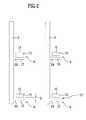
- FIG. 2is a top view of the column (or drain) address lines and corresponding drain electrodes of FIG. 1, this figure also illustrating the TFT source electrodes disposed adjacent the drain electrodes so as to define the TFT channels.
- FIG. 3is a top view of the pixel electrodes of FIG. 1 except for their extensions.
- FIG. 4is a side elevational cross-sectional view of the linear-shaped thin film transistors (TFTs) of FIGS. 1-2.
- FIG. 5is a side elevational cross-sectional view of the liquid crystal display of FIG. 1 .
- FIG. 6is a top or bottom view of the optional black matrix to be located on a substrate of the LCD of FIGS. 1-5, the black matrix to be located on the substrate not having the TFT array disposed thereon.
- FIG. 7is a side cross-sectional view of a portion of the LCD of FIGS. 1-6, this figure illustrating the pixel electrodes overlapping the column address lines.
- FIGS. 8-11are side elevational cross-sectional views illustrating how a TFT in an array according to this invention is manufactured.
- FIG. 1is a top view of four pixels in an array of an active matrix liquid crystal display (AMLCD) 2 according to an embodiment of this invention.
- This portion of the displayincludes pixel electrodes 3 , drain address lines 5 , gate address lines 7 , an array of four thin film transistors (TFTs) 9 , and auxiliary storage capacitors 11 associated with each pixel.
- Each storage capacitor 11is defined on one side by a gate line 7 and on the other side by an independent storage capacitor electrode 12 .
- Storage capacitor electrodes 12are formed along with drain electrodes 13 . As shown, the longitudinally extending edges of each pixel electrode 3 overlap drain lines 5 and gate lines 7 respectively along the edges thereof so as to increase the pixel aperture ratio (or pixel opening size) of the LCD.
- a pixel-line (PL) capacitoris defined by an electrode 3 on one side and the overlapped address line on the other.
- the dielectric disposed between the electrodes of these PL capacitorsis insulation layer 33 (see FIGS. 4 and 7 ).
- C PLis less than or equal to about 0.01 pF for a display with a pixel pitch of about 150 ⁇ m.
- C PLshould be scaled to a lower value as well because overlap areas 18 are smaller.
- the pixel aperture ratio of an LCDdecreases as the pixel pitch decreases as is known in the art.
- the pixel pitch of AMLCD 2may be from about 40 to 5,000 ⁇ m according to certain embodiments of this invention.
- the pixel pitch as known in the artis the distance between centers of adjacent pixels in the array.
- FIG. 2is a top view of drain address lines 5 of AMLCD 2 showing how extensions of address lines 5 form drain electrodes 13 of TFTs 9 .
- Each TFT 9 in the array of AMLCD 2includes source electrode 15 , drain electrode 13 , and gate electrode 17 .
- Gate electrode 17 of each TFT 9is formed by the corresponding gate address line 7 adjacent the TFT according to certain embodiments. According to other embodiments, the gate electrode 17 may be formed by a branch extending substantially perpendicular to the gate line.
- FIG. 3is a top view illustrating pixel electrodes 3 (absent their extension portions 38 ) of AMLCD 2 arranged in array form.
- FIGS. 2-3are provided so that FIG. 1 may be more easily interpreted.
- FIG. 4is a side elevational cross-sectional view of a single thin film transistor (TFT) 9 in the TFT array of AMLCD 2 , with each TFT 9 in the array being substantially the same according to preferred embodiments.
- Each linear TFT 9has a channel length “L” defined by the gap 27 between source electrode 15 and drain electrode 13 .
- Source electrode 15is connected to pixel electrode 3 by way of via or contact hole 35 so as to permit TFT 9 to act as a switching element and selectively energize a corresponding pixel in AMLCD 2 in order to provide image data to a viewer.
- An array of TFTs 9is provided as illustrated in FIG. 1 for AMLCD 2 .
- Each TFT 9 structureincludes substantially transparent substrate 19 (e.g. made of glass), metal gate electrode 17 , gate insulating layer or film 21 , semiconductor layer 23 (e.g. intrinsic amorphous silicon), doped semiconductor contact layer 25 , drain electrode 13 , source electrode 15 , substantially transparent insulation layer 33 , and a corresponding pixel electrode 3 .
- TFT channel 27 of length “L”is defined between source 15 and drain 13 .
- drain electrode 13is made up of drain metal layer 29 (e.g. Mo) which is deposited on substrate 19 over top of doped contact layer 25 .
- Contact film or layer 25may be, for example, amorphous silicon doped with an impurity such as phosphorous (i.e. n+a-Si) and is sandwiched between semiconductor layer 23 and drain metal layer 29 .
- Source electrode 15includes doped semiconductor contact layer 25 and source metal layer 31 .
- Metal layers 29 and 31may be of the same metal and deposited and patterned together according to certain embodiments of this invention. Alternatively, layer 29 may be deposited and patterned separately from layer 31 so that drain metal layer is of one metal (e.g. Mo) and source metal layer 31 is of another (e.g. Cr).
- Substantially transparent insulating layer 33 having a dielectric constant less than about 5.0is deposited as a sheet on substrate 19 so as to cover TFTs 9 and address lines 5 and 7 .
- Layer 33is formed of a photo-imageable material such as Fuji ClearTM or a photo-imageable type of BCB. Insulating layer 33 is continuous in the viewing area of the display except for vias or contact holes 35 and 36 formed therein to allow pixel electrodes 3 to contact corresponding TFT source electrodes and the storage capacitor electrodes respectively (i.e. each pixel includes two vias ( 35 and 36 ) in insulating layer 33 —one for the source electrode and the other for the storage capacitor).
- Layer 33has a dielectric constant ⁇ less than or equal to about 5.0 according to certain embodiments of this invention.
- layer 33has a dielectric constant of about 2.7 and is made of a photo-imageable type of Benzocyclobutene (BCB), an organic material available from Dow Chemical, for the purpose of reducing capacitive cross-talk (or capacitive coupling) between pixel electrodes 3 and the address lines in overlap areas 18 .
- Layer 33has a low dielectric constant and/or a relatively large thickness for the specific purpose of reducing C PL in overlap areas 18 .
- layer 33may be of a photo-imageable material known as Fuji ClearTM, which is an organic mixture including 2-Ethoxyethyl acetate (55-70%), methacrylate derivative copolymer (10-20%), and polyfunctional acrylate (10-20%).
- Fuji ClearTMis an organic mixture including 2-Ethoxyethyl acetate (55-70%), methacrylate derivative copolymer (10-20%), and polyfunctional acrylate (10-20%).
- vias 35 and 36are formed in insulation layer 33 by way of photo-imaging.
- Layer 33acts as a negative resist so that UV exposed areas remain on the substrate and areas of layer 33 unexposed to UV during photo-imaging are removed during developing.
- substantially transparent pixel electrodes 3(made of indium-tin-oxide or ITO) are deposited and patterned over layer 33 on substrate 19 so that the pixel electrodes 3 contact the corresponding source metal layers 31 of corresponding TFTs 9 through vias 35 as illustrated in FIG. 4 .
- Auxiliary vias 36are formed in layer 33 at the same time as vias 35 so that pixel electrodes 3 can contact storage capacitor electrodes 12 via pixel electrode extensions 38 . Peripheral lead areas and seal areas are also removed by photo-imaging.
- Insulating layer 33is deposited on substrate 19 over the address lines, storage capacitors, and TFTs to a thickness “d” of at least about 0.5 ⁇ m in overlap areas 18 .
- the thickness “d” of insulating layer 33is from about 1 to 2.5 ⁇ m.
- layer 33Another advantage of layer 33 , is that liquid crystal layer disclinations induced at pixel electrode 3 edges by the topography of TFTs 9 , storage capacitors, and address lines are substantially eliminated by planarization (i.e. few, if any, hills and valleys are present in the top surface of layer 33 ). Thus, the thickness of the LC layer is substantially maintained and display functionality is improved because electrodes 3 are substantially flat because of the substantial planarization of the surface of layer 33 adjacent the pixel electrodes 3 .
- the capacitive cross-talk problems of the prior art resulting from overly high C PL valuesare substantially reduced in areas 18 where pixel electrodes 3 overlap address lines 5 and/or 7 . Because layer 33 is disposed between pixel electrodes 3 and the overlapped address lines, the capacitive cross-talk problems of the prior art are substantially reduced or eliminated and increased pixel openings are achievable without sacrificing display performance (pixel isolation).
- Pixel opening sizes or the pixel aperture ratio of AMLCD 2is at least about 65% (preferably from about 68% to 80%) according to certain embodiments of this invention when the pixel pitch is about 150 ⁇ m. This will, of course, vary depending upon the pixel pitch of the display (pixel pitches of from about 40-500 ⁇ m may be used).
- Pixel electrodes 3overlap address lines 5 and 7 along the edges thereof as shown in FIG. 1 by an amount up to about 3 ⁇ m. In certain preferred embodiments of this invention, the overlap 18 of electrodes 3 over the edges of address lines 5 and 7 is designed to be from about 2 to 3 ⁇ m, with the end result after overetching being at least about 0.5 ⁇ m.
- the amount of overlapmay be designed to be from about 2-3 ⁇ m, with the resulting post-processing overlap being from about 0 to 2 ⁇ m.
- the overlap amountmay be adjusted in accordance with different LCD applications and pixel pitch sizes as will be appreciated by those of skill in the art.
- pixel electrodes 3may not overlap the address lines at all according to certain embodiments of this invention, although some overlap 18 is preferred. When no overlap occurs, the parasitic capacitance C PL between the address lines and the adjacent pixel electrode 3 is still minimized or reduced due to insulating layer 33 .
- substantially transparent substrate 19is provided.
- a gate metal layer or sheet(which results in gate electrodes 17 and lines 7 ) is deposited on the top surface (surface to be closest to the LC layer) of substrate 19 to a thickness of from about 1,000-5,000 ⁇ , most preferably to a thickness of about 2,500 ⁇ .
- the gate metal sheetis deposited by way of sputtering or vapor deposition.
- the gate metalmay be of tantalum (Ta) according to certain embodiments of this invention.
- Insulating substrate 19may be of glass, quartz, sapphire, or the like.
- the structure including substrate 19 and the deposited gate metalis then patterned by photolithography to the desired gate electrode 17 and gate address line 7 configuration.
- the upper surface of the gate metalis exposed in a window where the photoresist has not been retained.
- the gate metal (e.g. Ta) layeris then dry etched (preferably using reactive ion etching) in order to pattern the gate metal layer in accordance with the retained photoresist pattern.
- the structureis mounted in a known reactive ion etching (RIE) apparatus which is then purged and evacuated in accordance with known RIE procedures and etchants.
- RIEreactive ion etching
- This etching of the gate metal layeris preferably carried out until the gate metal is removed in center areas of the windows and is then permitted to proceed for an additional time (e.g. 20 to 40 seconds) of overetching to ensure that the gate metal is entirely removed from within the windows.
- the resultis gate address lines 7 (and gate electrodes 17 ) being left on substrate 19 .
- gate insulating or dielectric layer 21is deposited over substantially the entire substrate 19 preferably by plasma enhanced chemical vapor deposition (CVD) or some other process known to produce a high integrity dielectric.
- CVDplasma enhanced chemical vapor deposition
- FIG. 8The resulting structure is shown in FIG. 8 .
- Gate insulating layer 21is preferably silicon nitride (Si 3 N 4 ) but may also be silicon dioxide or other known dielectrics. Silicon Nitride has a dielectric constant of about 6.4.
- Gate insulating layer 21is deposited to a thickness of from about 2,000-3,000 ⁇ (preferably either about 2,000 ⁇ or 3,000 ⁇ ) according to certain embodiments.
- gate Ta layer 17which was deposited as the gate electrode and gate line layer (when originally about 2,500 ⁇ thick) is about 1,800 ⁇ thick and a newly created TaO layer is about 1,600 ⁇ .
- Anodizationtakes place after the gate line patterning and before further processing.
- gate insulating layer 21 over gate lines 7 and electrodes 17is made up of both the anodization created TaO layer and the silicon nitride layer.
- Other metals from which gate electrode 17 and address line layer 7 may be madeinclude Cr, Al, titanium, tungsten, copper, and combinations thereof.
- semiconductor layer 23is deposited on top of gate insulating layer 21 to a thickness of about 2,000 ⁇ .
- Semiconductor layer 23may be from about 1,000 ⁇ to 4,000 ⁇ thick in certain embodiments of this invention.
- doped (typically phosphorous doped, that is n+) amorphous silicon contact layer 25is deposited over intrinsic a-Si layer 23 in a known manner to a thickness of, for example, about 500 ⁇ .
- Doped contact layer 25may be from about 200 ⁇ to 1,000 ⁇ thick according to certain embodiments of this invention. The result is the FIG. 9 structure.
- Gate insulating layer 21 , semiconductor layer 23 and semiconductor contact layer 25may all be deposited on substrate 19 in the same deposition chamber without breaking the vacuum according to certain embodiments of this invention.
- the plasma discharge in the deposition chamberis stopped after the completion of the deposition of a particular layer (e.g. insulating layer 21 ) until the proper gas composition for deposition of the next layer (e.g. semiconductor layer 23 ) is established. Subsequently, the plasma discharge is re-established to deposit the next layer (e.g. semiconductor layer 23 ).
- layers 21 , 23 , and 25may be deposited in different chambers by any known method.
- the TFT island or areamay be formed by way of etching, for example, so that the TFT metal layers can be deposited thereon.
- one of the TFT metal source/drain layersmay be deposited before forming the TFT island.
- a source-drain metal sheet or layer(which results in drain metal layer 29 and source metal layer 31 ) is deposited on substrate 19 over top of semiconductor layer 23 and contact layer 25 .
- This source-drain metal layermay be chromium (Cr) or molybdenum (Mo) according to certain embodiments of this invention.
- Crchromium
- Momolybdenum
- the layeris deposited to a thickness of about 500-2,000 ⁇ , preferably about 1,000 ⁇ according to certain embodiments.
- molybdenumthe layer is deposited to a thickness of from about 2,000 to 7,000 ⁇ , preferably about 5,000 ⁇ .
- the deposited source drain metal layer sheetis then patterned (masked and etched) to form the source, drain, and storage capacitor electrodes. After patterning of the TFT source and drain electrodes, the result is the FIG. 10 TFT structure.
- a first metal layermay be deposited and patterned to form drain electrode portion 29 and storage capacitor electrode 12
- a second metal layermay be deposited and patterned to form source electrode portion 31 .
- source metal layer 31may be chromium (Cr) while drain metal 29 and storage capacitor electrode layer is Mo according to certain embodiments of this invention.
- Other metals which may be used for the source and drain metalsinclude titanium, Al, tungsten, tantalum, copper, or the like.
- Substantially transparent polymer insulating layer 33is then deposited onto substantially the entire substrate 19 by way of spin-coating according to certain embodiments of this invention.
- Layer 33may be of either photo-imageable BCB or Fuji ClearTM according to certain embodiments. Insulating layer 33 fills recesses generated upon formation of TFTs 9 and flattens the surface above substrate 19 at least about 60% according to certain embodiments. The result is the structure of FIG. 11 .
- Photo-imageable insulating layer 33acts as a negative resist layer according to certain embodiments of this invention so that no additional photoresist is needed to form vias 35 and 36 in layer 33 .
- layer 33is irradiated by ultraviolet (UV) rays (e.g. i rays of 365 nm), with UV irradiated areas of layer 33 to remain and non-exposed or non-radiated areas of layer 33 to be removed in developing.
- UVultraviolet
- a maskmay be used.
- layer 33is developed by using a known developing solution at a known concentration. In the developing stage, the areas of layer 33 corresponding to vias 35 and 36 are removed (i.e. dissolved) so as to form the vias in the insulating layer. After developing, the resist layer 33 is cured or subjected to postbaking (e.g. about 240 degrees C. for about one hour) to eliminate the solvent so that the layer 33 with the vias therein is resinified. Thus, no dry or wet etching is needed to form the vias in layer 33 . According to alternative embodiments, layer 33 may be a positive resist as opposed to a negative resist.
- Vias or apertures 35are thus formed in insulation layer 33 over top of (or adjacent) each source metal electrode 31 so as to permit the pixel electrodes 3 to electrically contact corresponding source electrodes 15 through vias 35 .
- Layer 33remains across the rest of the substrate or array except for the auxiliary capacitor vias and certain edge areas where contacts must be made or glueing done.
- a substantially transparent conducting layere.g. ITO
- pixel electrodes 3are deposited and patterned (photomasked and etched) on substrate 19 over top of layer 33 .
- patterninge.g. mask and etching
- pixel electrodes 3are left as shown in FIGS. 1 and 4.
- each pixel electrode 3contacts a TFT source electrode 31 as shown in FIG. 4 and a storage capacitor electrode 12 as shown in FIG. 1 .
- the resultis the active plate of FIGS. 1 and 4 including an array of TFTs.
- the pixel electrode layer(when made of ITO) is deposited to a thickness of from about 1,200 to 3,000 ⁇ (preferably about 1,400 ⁇ ) according to certain embodiments of this invention. Other known materials may be used as pixel electrode layer 3 .
- liquid crystal layer 45is disposed and sealed between the active plate and the passive plate as shown in FIG. 5, the passive plate including substrate 51 , polarizer 53 , electrode 49 , and orientation film 47 .
- pixel electrodes 3are patterned to a size so that they overlap both drain address lines 5 and gate address lines 7 along the edges thereof so as to result in an increased pixel aperture ratio for AMLCD 2 .
- the cross-talk problems of the prior artare substantially eliminated due to the presence of layer 33 in overlap areas 18 between pixel electrodes 3 and the address lines.
- the pixel electrodesmay only overlap one group of address lines (e.g. row lines) according to certain embodiments.
- FIG. 5is a side elevational cross-sectional view of AMLCD 2 (absent the TFTS, address lines, and black matrix).
- the twisted nematic displayincludes from the rear forward toward the viewer, rear polarizer 41 , substantially transparent substrate 19 , pixel electrodes 3 , rear orientation film 43 , liquid crystal layer 45 , front orientation film 47 , common electrode 49 , front substantially transparent substrate 51 , and finally front polarizer 53 .
- Polarizers 41 and 53may be arranged so that their transmission axes are either parallel or perpendicular to each other so as to define a normally black or normally white color AMLCD respectively.
- retarder(s)may also be provided.
- a backlightis provided rearward of polarizer 41 so that light emitted therefrom first goes through polarizer 41 , then through liquid crystal layer 45 and finally out of front polarizer 53 toward the viewer.
- Pixel electrodes 3selectively work in conjunction with common electrode 49 so as to selectively apply voltages across liquid crystal layer 45 so as to cause an image (preferably colored according to certain embodiments) to be viewed from the front of the display.
- FIG. 6illustrates an optional black matrix (BM) pattern 55 to be disposed on front substrate 51 for the purpose of overlaying address lines 5 and 7 and TFT channels 27 .
- BMblack matrix
- Black matrix structure 55includes vertically extending regions 56 and horizontally extending regions 57 . Regions 56 are aligned with drain lines 5 while regions 57 are aligned with gate lines 7 so as to prevent ambient light from penetrating the display. Additionally, black matrix 55 includes channel covering portions 58 which are aligned with TFT channels 27 for the purpose of preventing ambient light from reaching amorphous silicon semiconductor layer 23 through the channels. As commonly known in the art, the pixel openings 65 of the display are substantially defined by (i.e. bounded by) black matrix regions 56 and 57 .
- FIG. 7is a side elevational cross-sectional view of a portion of AMLCD 2 .
- the central pixel electrode 3 illustrated in FIG. 7overlaps both column or drain address lines 5 by an amount “w” thereby increasing the pixel electrode size relative to that of many prior art displays. Electrodes 3 are spaced from the address lines by a distance “d”. Also, black matrix portions 56 line up with address lines 5 so that the pixel aperture or opening for the center electrode 3 is defined in part by the distance between black matrix members 56 . Black matrix portions 56 and address lines 5 are both arranged so that their central axes correspond with the gaps between pixel electrodes 3 according to certain embodiments of this invention.
- the presence of layer 33substantially reduces the parasitic capacitance of the capacitor created between pixel electrodes 3 and address lines 5 in the overlap areas 18 as set forth above.
- Chart 1The values set forth above in Chart 1 are for a display wherein the side of each pixel electrode 3 which overlaps the address line is about 100 ⁇ m long. Thus, the area of overlap is about 100 ⁇ m long. Also, the dielectric constants ⁇ in Chart 1 and for insulating layer 33 .
- Distances “w” and “d”are shown in FIG. 7, with distance “w” being the width of the overlap and distance “d” the vertical spacing between the pixel electrodes and the overlapped address lines.
- the line pixel capacitance (fF)is less than about 20 fF, preferably less than or equal to about 12 fF, and most preferably less than or equal to about 7.0 fF according to this invention with the overlap areas and high pixel apertures.
Landscapes
- Physics & Mathematics (AREA)
- Nonlinear Science (AREA)
- Engineering & Computer Science (AREA)
- Mathematical Physics (AREA)
- Chemical & Material Sciences (AREA)
- Crystallography & Structural Chemistry (AREA)
- Microelectronics & Electronic Packaging (AREA)
- General Physics & Mathematics (AREA)
- Optics & Photonics (AREA)
- Power Engineering (AREA)
- Liquid Crystal (AREA)
- Thin Film Transistor (AREA)
- Devices For Indicating Variable Information By Combining Individual Elements (AREA)
Abstract
Description
This is a continuation of application Ser. No. 09/357,889, filed Jul. 21, 1999, now U.S. Pat. No. 6,307,215; which is a divisional of application Ser. No. 09/630,984, filed Apr. 12, 1996, now U.S. Pat. No. 6,372,534; which is a CIP of 09/470,271, filed Jun. 6, 1995, now abandoned, which are all incorporated herein by reference.
Additionally, this application is related to a commonly owned application filed simultaneously entitled LCD WITH BUS LINES OVERLAPPED BY PIXEL ELECTRODES AND PHOTO-IMAGEABLE INSULATING LAYER THEREBETWEEN.
This invention relates to a method of making a TFT array for a liquid crystal display (LCD) or image sensor having an increased pixel aperture ratio. More particularly, this invention relates to a method of making an array of TFTs wherein a photo-imageable insulating layer having a plurality of contact vias or apertures disposed therein is located between the address lines and pixel electrodes so that the pixel electrodes are permitted to overlap the row and column address lines without exposing the system to capacitive cross-talk.
Electronic matrix arrays find considerable application in X-ray image sensors and active matrix liquid crystal displays (AMLCDs). Such devices generally include X and Y (or row and column) address lines which are horizontally and vertically spaced apart and cross at an angle to one another thereby forming a plurality of crossover points. Associated with each crossover point is an element (e.g. pixel) to be selectively addressed. These elements in many instances are liquid crystal display pixels or alternatively the memory cells or pixels of an electronically adjustable memory array or X-ray sensor array.
Typically, a switching or isolation device such as a diode or thin film transistor (TFT) is associated with each array element or pixel. The isolation devices permit the individual pixels to be selectively addressed by the application of suitable potentials between respective pairs of the X and Y address lines. Thus, the TFTs act as switching elements for energizing or otherwise addressing corresponding pixel electrodes.
Amorphous silicon (a-Si) TFTs have found wide usage for isolation devices in liquid crystal display (LCD) arrays. Structurally, TFTs generally include substantially co-planar source and drain electrodes, a thin film semiconductor material (e.g. a-Si) disposed between the source and drain electrodes, and a gate electrode in proximity to the semiconductor but electrically insulated therefrom by a gate insulator. Current flow through the TFT between the source and drain is controlled by the application of voltage to the gate electrode. The voltage to the gate electrode produces an electric field which accumulates a charged region near the semiconductor-gate insulator interface. This charged region forms a current conducting channel in the semiconductor through which current is conducted. Thus, by controlling the voltage to the gate and drain electrodes, the pixels of an AMLCD may be switched on and off in a known manner.
Typically, pixel aperture ratios (i.e. pixel openings) in non-overlapping AMLCDs are only about 50% or less. As a result, either display luminance is limited or backlight power consumption is excessive, thereby precluding or limiting use in certain applications. Thus, it is known in the art that it is desirable to increase the pixel aperture ratio or pixel opening size of LCDs to as high a value as possible so as to circumvent these problems. The higher the pixel aperture ratio (or pixel opening size) of a display, for example, the higher the display transmission. Thus, by increasing the pixel aperture ratio of a display, transmission may be increased using the same backlight power, or alternatively, the backlight power consumption may be reduced while maintaining the same display luminance.
It is known to overlap pixel electrodes over address lines in order to increase the pixel aperture ratio. For example, “High-Aperture TFT Array Structures” by K. Suzuki discusses an LCD having an ITO shield plane configuration having a pixel aperture ratio of 40% and pixel electrodes which overlap signal bus lines. An ITO pattern in Suzuki located between the pixel electrodes and the signal lines functions as a ground plane so as to reduce coupling capacitance between the signal lines and the pixel electrode. Unfortunately, it is not always desirable to have a shield electrode disposed along the length of the signal lines as in Suzuki due to production and cost considerations. The disposition of the shield layer as described by Suzuki requires extra processing steps and thus presents yield problems. Accordingly, there exists a need in the art for a LCD with an increased pixel aperture ratio which does not require an ITO shield plane structure to be disposed between the signal lines and pixel electrode.
It is old and well-known to make TFT arrays for LCDs wherein address lines and overlapping pixel electrodes are insulated from one another by an insulating layer. For example, see U.S. Pat. Nos. 5,055,899; 5,182,620; 5,414,547; 5,426,523; 5,446,562; 5,453,857; and 5,457,553.
U.S. Pat. No. 5,182,620 discloses an AMLCD including pixel electrodes which at least partially overlay the address lines and additional capacitor lines thereby achieving a larger numerical aperture for the display. The pixel electrodes are insulated from the address lines which they overlap by an insulating layer formed of silicon oxide or silicon nitride. Unfortunately, the method of making this display as well as the resulting structure are less than desirable because: (i) chemical vapor deposition (CVD) is required to deposit the silicon oxide or silicon nitride insulating film; and (ii) silicon oxide and silicon nitride are not photo-imageable (i.e. contact holes or vias must be formed in such insulating layers by way of etching). As a result of these two problems, the manufacturing process is both expensive and requires more steps than would be otherwise desirable. For example, in order to etch the contact holes in an insulating layer, an additional photo-resist coating step is required and the user must be concerned about layers underneath the insulating layer during etching. With respect to CVD, this is a deposition process requiring expensive equipment.
U.S. Pat. No. 5,453,857 discloses an AMLCD having a TFT array with pixel electrodes formed in an overlapping relation with source signal lines through an insulating thin film. The insulating thin film formed between the signal lines and the pixel electrodes is made of either SiNx, SiO2, TaOxor Al2O3. Unfortunately, the method of making the array and resulting display of the '857 patent suffers from the same problems discussed above with respect to the '620 patent. None of the possible insulating layer materials are photo-imageable and etching is required.
U.S. Pat. No. 5,055,899 discloses a TFT array including an insulating film disposed between the address lines and pixel electrodes. Again, etching is required to form the vias in the insulating film. This is undesirable.
U.S. Pat. No. 5,426,523 discloses an LCD including overlapping pixel electrodes and source bus lines, with a silicon oxide insulating film disposed therebetween. Silicon oxide is not photo-imageable and thus necessitates a prolonged and more difficult manufacturing process for the TFT array and resulting AMLCD.
It is apparent from the above that there exists a need in the art for an improved method for manufacturing a TFT array and/or resulting LCD having an increased pixel aperture ratio and little capacitive cross-talk. The method of manufacture, which is improved relative to the prior art, should include forming a photo-imageable insulating layer between pixel electrodes and overlapped bus lines and the vias therein by way of photo-imaging as opposed to resist coating, exposure and developing, and wet or dry etching. The method should be simpler, cheaper, and more efficient to carry out.
It is a purpose of this invention to fulfill the above-described needs in the art, as well as other needs which will become apparent to the skilled artisan from the following detailed description of this invention.
Generally speaking, this invention fulfills the above-described needs in the art by providing a method of making an array of a-Si semiconductor based thin film transitors (TFTs), the method comprising the steps of:
providing a first substantially transparent substrate;
forming an array of TFTs and corresponding address lines on the first substrate;
depositing an organic photo-imageable insulating layer over the TFT array and corresponding address lines;
photo-imaging the insulating layer in order to form a first array of vias or contact holes therein; and
forming an array of electrode members on the first substrate over the photo-imaged insulating layer so that the electrode members in the array are in communication with the TFTs through the first array of vias or contact holes.
In certain preferred embodiments, the method includes the step of overlapping the address lines with the electrode members so that the photo-imaged insulating layer is disposed therebetween so as to increase the pixel aperture and reduce cross-talk.
In still further preferred embodiments, the method comprises the steps of: (i) using the TFT array in one of a liquid crystal display and an X-ray image sensor, and (ii) forming the insulating layer so as to include one of photo-imageable Benzocyclobutene (BCB) and 2-Ethoxyethyl acetate.
This invention further fulfills the above-described needs in the art by providing a method of making a liquid crystal display including an array of semiconductor switching elements, the method comprising the steps of:
a) providing a first substrate;
b) providing an array of semiconductor based switching elements and corresponding address lines on the first substrate;
c) spin coating an organic photo-imageable insulating layer on the first substrate over the switching elements and address lines;
d) photo-imaging the insulating layer in order to form a first group of vias or contact holes therein, each via in the first group corresponding to one of the switching elements; and
e) forming an array of pixel electrodes over the photo-imaged insulating layer so that each pixel electrode communicates with one of the switching elements through one of the vias in the insulating layer.
This invention still further fulfills the above-described needs in the art by providing a method of making a TFT array comprising the steps of:
a) providing a first substantially transparent substrate;
b) forming a plurality of TFT gate electrodes connected to gate lines on the substrate;
c) forming a gate insulating layer over the gate electrodes;
d) forming and patterning a semiconductor layer over each of the gate electrodes in TFT areas;
e) forming TFT source and drain electrodes in each TFT area with a TFT channel defined therebetween, and a plurality of corresponding drain lines, thereby forming an array of TFTs on the first substrate;
f) depositing a photo-imageable insulating layer over a substantial portion of the substrate so as to cover substantial portions of the gate and drain lines and the TFTs in the array;
g) photo-imaging the insulating layer so as to form a plurality of vias or contact holes therein, at least one via corresponding to each TFT in the array;
h) forming a plurality of pixel electrodes over the insulating layer so that each pixel electrode is in communication with the source electrode of a corresponding TFT through one of the vias; and
i) forming the pixel electrodes on the substrate so that each pixel electrode overlaps at least one of the drain and gate lines whereby the pixel electrodes are insulated from the address lines in the overlap areas by the photo-imaged insulating layer.
This invention will now be described with reference to certain embodiments thereof as illustrated in the following drawings.
FIG. 1 is a top view of an AMLCD according to this invention, this figure illustrating pixel electrodes overlapping surrounding row and column address lines along their respective lengths throughout the display's pixel area so as to increase the pixel aperture ratio of the display.
FIG. 2 is a top view of the column (or drain) address lines and corresponding drain electrodes of FIG. 1, this figure also illustrating the TFT source electrodes disposed adjacent the drain electrodes so as to define the TFT channels.
FIG. 3 is a top view of the pixel electrodes of FIG. 1 except for their extensions.
FIG. 4 is a side elevational cross-sectional view of the linear-shaped thin film transistors (TFTs) of FIGS. 1-2.
FIG. 5 is a side elevational cross-sectional view of the liquid crystal display of FIG.1.
FIG. 6 is a top or bottom view of the optional black matrix to be located on a substrate of the LCD of FIGS. 1-5, the black matrix to be located on the substrate not having the TFT array disposed thereon.
FIG. 7 is a side cross-sectional view of a portion of the LCD of FIGS. 1-6, this figure illustrating the pixel electrodes overlapping the column address lines.
FIGS. 8-11 are side elevational cross-sectional views illustrating how a TFT in an array according to this invention is manufactured.
Referring now more particularly to the accompanying drawings in which like reference numerals indicate like parts throughout the several views.
FIG. 1 is a top view of four pixels in an array of an active matrix liquid crystal display (AMLCD)2 according to an embodiment of this invention. This portion of the display includespixel electrodes 3,drain address lines 5,gate address lines 7, an array of four thin film transistors (TFTs)9, andauxiliary storage capacitors 11 associated with each pixel. Eachstorage capacitor 11 is defined on one side by agate line 7 and on the other side by an independentstorage capacitor electrode 12.Storage capacitor electrodes 12 are formed along withdrain electrodes 13. As shown, the longitudinally extending edges of eachpixel electrode 3overlap drain lines 5 andgate lines 7 respectively along the edges thereof so as to increase the pixel aperture ratio (or pixel opening size) of the LCD.
In the areas ofoverlap 18 betweenpixel electrodes 3 and address orbus lines electrode 3 on one side and the overlapped address line on the other. The dielectric disposed between the electrodes of these PL capacitors is insulation layer33 (see FIGS.4 and7). The parasitic capacitance CPLof these capacitors is defined by the equation:

where “d” is the thickness oflayer 33, ε is the dielectric constant oflayer 33, ε0is the constant 8.85×10⁻¹⁴F/cm (permitivity in vacuum), and “A” is the area of the PL capacitor inoverlap areas 18. The fringing capacitance may also be taken into consideration in a known manner. See Chart 1 below for certain embodiments. Also, according to other embodiments, CPLis less than or equal to about 0.01 pF for a display with a pixel pitch of about 150 μm. When the pixel pitch is smaller, CPLshould be scaled to a lower value as well becauseoverlap areas 18 are smaller. Additionally, the pixel aperture ratio of an LCD decreases as the pixel pitch decreases as is known in the art. The pixel pitch ofAMLCD 2 may be from about 40 to 5,000 μm according to certain embodiments of this invention. The pixel pitch as known in the art is the distance between centers of adjacent pixels in the array.
FIG. 2 is a top view ofdrain address lines 5 ofAMLCD 2 showing how extensions ofaddress lines 5form drain electrodes 13 ofTFTs 9. EachTFT 9 in the array ofAMLCD 2 includessource electrode 15,drain electrode 13, andgate electrode 17.Gate electrode 17 of eachTFT 9 is formed by the correspondinggate address line 7 adjacent the TFT according to certain embodiments. According to other embodiments, thegate electrode 17 may be formed by a branch extending substantially perpendicular to the gate line.
FIG. 3 is a top view illustrating pixel electrodes3 (absent their extension portions38) ofAMLCD 2 arranged in array form. FIGS. 2-3 are provided so that FIG. 1 may be more easily interpreted.
FIG. 4 is a side elevational cross-sectional view of a single thin film transistor (TFT)9 in the TFT array ofAMLCD 2, with eachTFT 9 in the array being substantially the same according to preferred embodiments. Eachlinear TFT 9 has a channel length “L” defined by thegap 27 betweensource electrode 15 anddrain electrode 13.Source electrode 15 is connected topixel electrode 3 by way of via orcontact hole 35 so as to permitTFT 9 to act as a switching element and selectively energize a corresponding pixel inAMLCD 2 in order to provide image data to a viewer. An array ofTFTs 9 is provided as illustrated in FIG. 1 forAMLCD 2.
EachTFT 9 structure includes substantially transparent substrate19 (e.g. made of glass),metal gate electrode 17, gate insulating layer orfilm 21, semiconductor layer23 (e.g. intrinsic amorphous silicon), dopedsemiconductor contact layer 25,drain electrode 13,source electrode 15, substantiallytransparent insulation layer 33, and acorresponding pixel electrode 3.TFT channel 27 of length “L” is defined betweensource 15 anddrain 13.
As shown in FIG. 4,drain electrode 13 is made up of drain metal layer29 (e.g. Mo) which is deposited onsubstrate 19 over top ofdoped contact layer 25. Contact film orlayer 25 may be, for example, amorphous silicon doped with an impurity such as phosphorous (i.e. n+a-Si) and is sandwiched betweensemiconductor layer 23 and drainmetal layer 29.Source electrode 15 includes dopedsemiconductor contact layer 25 andsource metal layer 31. Metal layers29 and31 may be of the same metal and deposited and patterned together according to certain embodiments of this invention. Alternatively,layer 29 may be deposited and patterned separately fromlayer 31 so that drain metal layer is of one metal (e.g. Mo) andsource metal layer 31 is of another (e.g. Cr).
Substantially transparent insulatinglayer 33 having a dielectric constant less than about 5.0 is deposited as a sheet onsubstrate 19 so as to coverTFTs 9 andaddress lines Layer 33 is formed of a photo-imageable material such as Fuji Clear™ or a photo-imageable type of BCB. Insulatinglayer 33 is continuous in the viewing area of the display except for vias or contact holes35 and36 formed therein to allowpixel electrodes 3 to contact corresponding TFT source electrodes and the storage capacitor electrodes respectively (i.e. each pixel includes two vias (35 and36) in insulatinglayer 33—one for the source electrode and the other for the storage capacitor).
Alternatively,layer 33 may be of a photo-imageable material known as Fuji Clear™, which is an organic mixture including 2-Ethoxyethyl acetate (55-70%), methacrylate derivative copolymer (10-20%), and polyfunctional acrylate (10-20%).
Following the deposition ofinsulation layer 33 onsubstrate 19 over top ofTFTs 9 andaddress lines insulation layer 33 by way of photo-imaging.Layer 33 acts as a negative resist so that UV exposed areas remain on the substrate and areas oflayer 33 unexposed to UV during photo-imaging are removed during developing. Following the forming ofvias layer 33 onsubstrate 19 so that thepixel electrodes 3 contact the corresponding source metal layers31 ofcorresponding TFTs 9 throughvias 35 as illustrated in FIG.4. Auxiliary vias36 (see FIG. 1) are formed inlayer 33 at the same time asvias 35 so thatpixel electrodes 3 can contactstorage capacitor electrodes 12 viapixel electrode extensions 38. Peripheral lead areas and seal areas are also removed by photo-imaging.
Insulatinglayer 33 is deposited onsubstrate 19 over the address lines, storage capacitors, and TFTs to a thickness “d” of at least about 0.5 μm inoverlap areas 18. In preferred embodiments, the thickness “d” of insulatinglayer 33 is from about 1 to 2.5 μm.
Another advantage oflayer 33, is that liquid crystal layer disclinations induced atpixel electrode 3 edges by the topography ofTFTs 9, storage capacitors, and address lines are substantially eliminated by planarization (i.e. few, if any, hills and valleys are present in the top surface of layer33). Thus, the thickness of the LC layer is substantially maintained and display functionality is improved becauseelectrodes 3 are substantially flat because of the substantial planarization of the surface oflayer 33 adjacent thepixel electrodes 3.
Because of the low dielectric constant ε and/or relatively high thickness “d” oflayer 33, the capacitive cross-talk problems of the prior art resulting from overly high CPLvalues are substantially reduced inareas 18 wherepixel electrodes 3overlap address lines 5 and/or7. Becauselayer 33 is disposed betweenpixel electrodes 3 and the overlapped address lines, the capacitive cross-talk problems of the prior art are substantially reduced or eliminated and increased pixel openings are achievable without sacrificing display performance (pixel isolation).
Pixel opening sizes or the pixel aperture ratio ofAMLCD 2 is at least about 65% (preferably from about 68% to 80%) according to certain embodiments of this invention when the pixel pitch is about 150 μm. This will, of course, vary depending upon the pixel pitch of the display (pixel pitches of from about 40-500 μm may be used).Pixel electrodes 3overlap address lines overlap 18 ofelectrodes 3 over the edges ofaddress lines
In certain situations, after etching and processing,pixel electrodes 3 may not overlap the address lines at all according to certain embodiments of this invention, although some overlap18 is preferred. When no overlap occurs, the parasitic capacitance CPLbetween the address lines and theadjacent pixel electrode 3 is still minimized or reduced due to insulatinglayer 33.
Referring now to FIGS. 4-5 and8-11, it will be described howAMLCD 2 including the array of TFT structures and corresponding address lines is made according to an embodiment of this invention. Firstly, substantiallytransparent substrate 19 is provided. Next, a gate metal layer or sheet (which results ingate electrodes 17 and lines7) is deposited on the top surface (surface to be closest to the LC layer) ofsubstrate 19 to a thickness of from about 1,000-5,000 Å, most preferably to a thickness of about 2,500 Å. The gate metal sheet is deposited by way of sputtering or vapor deposition. The gate metal may be of tantalum (Ta) according to certain embodiments of this invention. Insulatingsubstrate 19 may be of glass, quartz, sapphire, or the like.
Thestructure including substrate 19 and the deposited gate metal is then patterned by photolithography to the desiredgate electrode 17 andgate address line 7 configuration. The upper surface of the gate metal is exposed in a window where the photoresist has not been retained.
The gate metal (e.g. Ta) layer is then dry etched (preferably using reactive ion etching) in order to pattern the gate metal layer in accordance with the retained photoresist pattern. To do this, the structure is mounted in a known reactive ion etching (RIE) apparatus which is then purged and evacuated in accordance with known RIE procedures and etchants. This etching of the gate metal layer is preferably carried out until the gate metal is removed in center areas of the windows and is then permitted to proceed for an additional time (e.g. 20 to 40 seconds) of overetching to ensure that the gate metal is entirely removed from within the windows. The result is gate address lines7 (and gate electrodes17) being left onsubstrate 19.
Aftergate address lines 7 are deposited and patterned on top ofsubstrate 19 in the above-described manner, gate insulating ordielectric layer 21 is deposited over substantially theentire substrate 19 preferably by plasma enhanced chemical vapor deposition (CVD) or some other process known to produce a high integrity dielectric. The resulting structure is shown in FIG.8.Gate insulating layer 21 is preferably silicon nitride (Si3N4) but may also be silicon dioxide or other known dielectrics. Silicon Nitride has a dielectric constant of about 6.4.Gate insulating layer 21 is deposited to a thickness of from about 2,000-3,000 Å (preferably either about 2,000 Å or 3,000 Å) according to certain embodiments.
It is noted that after anodization (which is optional),gate Ta layer 17 which was deposited as the gate electrode and gate line layer (when originally about 2,500 Å thick) is about 1,800 Å thick and a newly created TaO layer is about 1,600 Å. Anodization takes place after the gate line patterning and before further processing. Thus,gate insulating layer 21 overgate lines 7 andelectrodes 17 is made up of both the anodization created TaO layer and the silicon nitride layer. Other metals from whichgate electrode 17 andaddress line layer 7 may be made include Cr, Al, titanium, tungsten, copper, and combinations thereof.
Next, aftergate insulating layer 21 has been deposited (FIG.8), semiconductor (e.g. intrinsic a-Si)layer 23 is deposited on top ofgate insulating layer 21 to a thickness of about 2,000 Å.Semiconductor layer 23 may be from about 1,000 Å to 4,000 Å thick in certain embodiments of this invention. Then, doped (typically phosphorous doped, that is n+) amorphoussilicon contact layer 25 is deposited overintrinsic a-Si layer 23 in a known manner to a thickness of, for example, about 500 Å.Doped contact layer 25 may be from about 200 Å to 1,000 Å thick according to certain embodiments of this invention. The result is the FIG. 9 structure.
Following the formation of the FIG. 9 structure, the TFT island or area may be formed by way of etching, for example, so that the TFT metal layers can be deposited thereon. Optionally, one of the TFT metal source/drain layers may be deposited before forming the TFT island.
According to preferred embodiments, following the formation of the TFT island from the FIG. 9 structure, a source-drain metal sheet or layer (which results indrain metal layer 29 and source metal layer31) is deposited onsubstrate 19 over top ofsemiconductor layer 23 andcontact layer 25. This source-drain metal layer may be chromium (Cr) or molybdenum (Mo) according to certain embodiments of this invention. When chromium, the layer is deposited to a thickness of about 500-2,000 Å, preferably about 1,000 Å according to certain embodiments. When molybdenum, the layer is deposited to a thickness of from about 2,000 to 7,000 Å, preferably about 5,000 Å. The deposited source drain metal layer sheet is then patterned (masked and etched) to form the source, drain, and storage capacitor electrodes. After patterning of the TFT source and drain electrodes, the result is the FIG. 10 TFT structure.
Alternatively, a first metal layer may be deposited and patterned to formdrain electrode portion 29 andstorage capacitor electrode 12, and a second metal layer may be deposited and patterned to formsource electrode portion 31. Thus, for example,source metal layer 31 may be chromium (Cr) whiledrain metal 29 and storage capacitor electrode layer is Mo according to certain embodiments of this invention. Other metals which may be used for the source and drain metals include titanium, Al, tungsten, tantalum, copper, or the like.
After patterning of drain andsource portions contact layer 25 is etched in thechannel 27 area and inevitably a bit ofsemiconductor layer 23 is etched along with it. The result isTFT 9 withchannel 27 as shown in FIGS. 4 and 10.
Substantially transparentpolymer insulating layer 33 is then deposited onto substantially theentire substrate 19 by way of spin-coating according to certain embodiments of this invention.Layer 33 may be of either photo-imageable BCB or Fuji Clear™ according to certain embodiments. Insulatinglayer 33 fills recesses generated upon formation ofTFTs 9 and flattens the surface abovesubstrate 19 at least about 60% according to certain embodiments. The result is the structure of FIG.11.
Photo-imageable insulating layer 33 acts as a negative resist layer according to certain embodiments of this invention so that no additional photoresist is needed to formvias layer 33. In order to form the vias,layer 33 is irradiated by ultraviolet (UV) rays (e.g. i rays of 365 nm), with UV irradiated areas oflayer 33 to remain and non-exposed or non-radiated areas oflayer 33 to be removed in developing. A mask may be used. Thus, the areas of the negative resist33 corresponding tovias layer 33 across the substrate is exposed to UV.
Following exposure of layer33 (except in the via or contact hole areas),layer 33 is developed by using a known developing solution at a known concentration. In the developing stage, the areas oflayer 33 corresponding tovias layer 33 is cured or subjected to postbaking (e.g. about 240 degrees C. for about one hour) to eliminate the solvent so that thelayer 33 with the vias therein is resinified. Thus, no dry or wet etching is needed to form the vias inlayer 33. According to alternative embodiments,layer 33 may be a positive resist as opposed to a negative resist.
Vias orapertures 35 are thus formed ininsulation layer 33 over top of (or adjacent) eachsource metal electrode 31 so as to permit thepixel electrodes 3 to electrically contact correspondingsource electrodes 15 throughvias 35.Layer 33 remains across the rest of the substrate or array except for the auxiliary capacitor vias and certain edge areas where contacts must be made or glueing done.
After vias35 and36 are formed inlayer 33, a substantially transparent conducting layer (e.g. ITO) which results inpixel electrodes 3 is deposited and patterned (photomasked and etched) onsubstrate 19 over top oflayer 33. After patterning (e.g. mask and etching) of this substantially transparent conducting layer,pixel electrodes 3 are left as shown in FIGS. 1 and 4. As a result ofvias layer 33, eachpixel electrode 3 contacts aTFT source electrode 31 as shown in FIG. 4 and astorage capacitor electrode 12 as shown in FIG.1. The result is the active plate of FIGS. 1 and 4 including an array of TFTs. The pixel electrode layer (when made of ITO) is deposited to a thickness of from about 1,200 to 3,000 Å (preferably about 1,400 Å) according to certain embodiments of this invention. Other known materials may be used aspixel electrode layer 3.
After formation of the active plate,liquid crystal layer 45 is disposed and sealed between the active plate and the passive plate as shown in FIG. 5, the passiveplate including substrate 51,polarizer 53,electrode 49, andorientation film 47.
As shown in FIG. 1,pixel electrodes 3 are patterned to a size so that they overlap bothdrain address lines 5 andgate address lines 7 along the edges thereof so as to result in an increased pixel aperture ratio forAMLCD 2. The cross-talk problems of the prior art are substantially eliminated due to the presence oflayer 33 inoverlap areas 18 betweenpixel electrodes 3 and the address lines. Alternatively, the pixel electrodes may only overlap one group of address lines (e.g. row lines) according to certain embodiments.
FIG. 5 is a side elevational cross-sectional view of AMLCD2 (absent the TFTS, address lines, and black matrix). As shown, the twisted nematic display includes from the rear forward toward the viewer,rear polarizer 41, substantiallytransparent substrate 19,pixel electrodes 3,rear orientation film 43,liquid crystal layer 45,front orientation film 47,common electrode 49, front substantiallytransparent substrate 51, and finallyfront polarizer 53. Polarizers41 and53 may be arranged so that their transmission axes are either parallel or perpendicular to each other so as to define a normally black or normally white color AMLCD respectively. optionally, retarder(s) may also be provided.
Typically, a backlight is provided rearward ofpolarizer 41 so that light emitted therefrom first goes throughpolarizer 41, then throughliquid crystal layer 45 and finally out offront polarizer 53 toward the viewer.Pixel electrodes 3 selectively work in conjunction withcommon electrode 49 so as to selectively apply voltages acrossliquid crystal layer 45 so as to cause an image (preferably colored according to certain embodiments) to be viewed from the front of the display.
FIG. 6 illustrates an optional black matrix (BM) pattern55 to be disposed onfront substrate 51 for the purpose of overlayingaddress lines TFT channels 27. When the ITO of thepixel electrodes 3 overlaps the address lines, the address lines themselves are effectively the black matrix blocking light in the interpixel areas. However, low reflectance black matrix55 with a larger than normal opening is still useful on the top (or passive) plate in order to reduce specular reflectance and to prevent ambient light incidence on the TFT channels. Therefore, the pixel aperture ratio of the display can be made larger because the pixel electrode area is larger and the overlap between the pixel electrodes on the active plate and black matrix55 on the passive plate can be reduced.
Black matrix structure55 includes vertically extendingregions 56 and horizontally extending regions57.Regions 56 are aligned withdrain lines 5 while regions57 are aligned withgate lines 7 so as to prevent ambient light from penetrating the display. Additionally, black matrix55 includes channel covering portions58 which are aligned withTFT channels 27 for the purpose of preventing ambient light from reaching amorphoussilicon semiconductor layer 23 through the channels. As commonly known in the art, thepixel openings 65 of the display are substantially defined by (i.e. bounded by)black matrix regions 56 and57.
FIG. 7 is a side elevational cross-sectional view of a portion ofAMLCD 2. As shown, thecentral pixel electrode 3 illustrated in FIG. 7 overlaps both column or drainaddress lines 5 by an amount “w” thereby increasing the pixel electrode size relative to that of many prior art displays.Electrodes 3 are spaced from the address lines by a distance “d”. Also,black matrix portions 56 line up withaddress lines 5 so that the pixel aperture or opening for thecenter electrode 3 is defined in part by the distance betweenblack matrix members 56.Black matrix portions 56 andaddress lines 5 are both arranged so that their central axes correspond with the gaps betweenpixel electrodes 3 according to certain embodiments of this invention. The presence oflayer 33 substantially reduces the parasitic capacitance of the capacitor created betweenpixel electrodes 3 andaddress lines 5 in theoverlap areas 18 as set forth above.
This invention will now be described with respect to 15 certain examples set forth below in Chart 1.
| CHART 1 |
| Insulating | Overlap | Line- | ||||
| Layer | ||||||
| 33 | distance | Distance | Capacitance | Dielectric | ||
| Material | “w” | “d” | (fF) | Constant ∈ | ||
| Example 1 | BCB | 1 | 2 μm | 4.5 | 2.7 |
| Example 2 | 2 | 2 μm | 6.9 | 2.7 | |
| Example 3 | BCB | 1 μm | 1 μm | 6.9 | 2.7 |
| Example 4 | 2 μm | 1 μm | 11.7 | 2.7 | |
| Example 5 | Fuji | 1 | 2 μm | 7.5 | 4.5 |
| Clear ™ | |||||
| Example 6 | 2 | 2 μm | 11.5 | 4.5 | |
| Clear ™ | |||||
| Example 7 | Fuji | 1 μm | 1 μm | 11.5 | 4.5 |
| Clear ™ | |||||
| Example 8 | 2 μm | 1 μm | 19.4 | 4.5 | |
| Clear ™ | |||||
The values set forth above in Chart 1 are for a display wherein the side of eachpixel electrode 3 which overlaps the address line is about 100 μm long. Thus, the area of overlap is about 100 μm long. Also, the dielectric constants ε in Chart 1 and for insulatinglayer 33.
Distances “w” and “d” are shown in FIG. 7, with distance “w” being the width of the overlap and distance “d” the vertical spacing between the pixel electrodes and the overlapped address lines.
Compare the values in Chart1 with a conventional coplanar LCD in which the pixel electrodes are substantially coplanar with the address lines and spaced therefrom, such a conventional LCD having a line-pixel capacitance of about 11.8 fF (caused in part by the LC material) when the electrodes are spaced laterally from the address lines by about 5 μm, and about 9.6 fF when the lateral spacing is about 10 μm. Thus, the high aperture LCDs of Examples 1-8 have a higher pixel aperture ratio than conventional LCDs without suffering from substantially higher line-pixel capacitance values. The capacitance values set forth above in Chart 1 were arrived at from the CPLequation above in combination with taking into consideration the fringing capacitance in a known manner.
The line pixel capacitance (fF) is less than about 20 fF, preferably less than or equal to about 12 fF, and most preferably less than or equal to about 7.0 fF according to this invention with the overlap areas and high pixel apertures.
Once given the above disclosure, many other features, modifications, and improvements will become apparent to the skilled artisan. Such other features, modifications, and improvements are, therefore, considered to be a part of this invention, the scope of which is to be determined by the following claims.
Claims (13)
1. A liquid crystal display device comprising:
a substrate;
an array of transistors on said substrate;
a plurality of gate and data lines connected to said transistors;
an array of pixel electrodes on said substrate;
a plurality of pixel electrodes overlapping at least one of the gate and data lines; and
a photo-imageable insulating layer on said substrate between said gate and data lines and said pixel electrodes at least in the areas of overlap and areas adjacent source electrodes of the transistors,
wherein said photo-imageable insulating layer has a dielectric constant less than about 5.0, and a first group of contact vias defined therein by photo-imaging, wherein said pixel electrodes are in electrical communication with corresponding transistor source electrodes through corresponding contact vias of said first group that are defined in said insulating layer.
2. The liquid crystal display device according toclaim 1 , wherein the photo-imageable insulating layer is planarized adjacent the pixel electrodes.
3. The liquid crystal display device according toclaim 1 , wherein a pixel aperture ratio is at least about 65%.
4. The liquid crystal display device according toclaim 1 , wherein the pixel electrode overlaps one of the drain and gate lines up to about 3 μm.
5. The liquid crystal display device according toclaim 1 , wherein the thickness of the gate electrodes and the gate lines is about 2,500Å.
6. The liquid crystal display device according toclaim 1 , further comprising a semiconductor layer on top of the gate insulating layer.
7. The liquid crystal display device according toclaim 6 , wherein the semiconductor layer includes intrinsic a-Si.
8. The liquid crystal display device according toclaim 7 , wherein the thickness of the semiconductor layer is about 2,000Å.
9. The liquid crystal display device according toclaim 6 , further comprising a contact layer over the semiconductor layer.
10. The liquid crystal display device according toclaim 9 , wherein the contact layer includes amorphous silicon.
11. The liquid crystal display device according toclaim 10 , wherein the thickness of the contact layer is about 500Å.
12. The liquid crystal display device according toclaim 1 , wherein the thickness of the pixel electrodes is about 1,400Å.
13. The liquid crystal display device according toclaim 1 , wherein a pixel pitch is about 150μm.
Priority Applications (1)
| Application Number | Priority Date | Filing Date | Title |
|---|---|---|---|
| US09/781,397US6515300B2 (en) | 1995-06-06 | 2001-02-13 | Method of making a TFT array with photo-imageable insulating layer over address lines |
Applications Claiming Priority (4)
| Application Number | Priority Date | Filing Date | Title |
|---|---|---|---|
| US47027195A | 1995-06-06 | 1995-06-06 | |
| US08/630,984US6372534B1 (en) | 1995-06-06 | 1996-04-12 | Method of making a TFT array with photo-imageable insulating layer over address lines |
| US09/357,889US6307215B1 (en) | 1995-06-06 | 1999-07-21 | TFT array with photo-imageable insulating layer over address lines |
| US09/781,397US6515300B2 (en) | 1995-06-06 | 2001-02-13 | Method of making a TFT array with photo-imageable insulating layer over address lines |
Related Parent Applications (1)
| Application Number | Title | Priority Date | Filing Date |
|---|---|---|---|
| US09/357,889ContinuationUS6307215B1 (en) | 1995-06-06 | 1999-07-21 | TFT array with photo-imageable insulating layer over address lines |
Publications (2)
| Publication Number | Publication Date |
|---|---|
| US20010029057A1 US20010029057A1 (en) | 2001-10-11 |
| US6515300B2true US6515300B2 (en) | 2003-02-04 |
Family
ID=23866927
Family Applications (15)
| Application Number | Title | Priority Date | Filing Date |
|---|---|---|---|
| US08/630,984Expired - LifetimeUS6372534B1 (en) | 1995-06-06 | 1996-04-12 | Method of making a TFT array with photo-imageable insulating layer over address lines |
| US08/631,455Expired - LifetimeUS5641974A (en) | 1995-06-06 | 1996-04-12 | LCD with bus lines overlapped by pixel electrodes and photo-imageable insulating layer therebetween |
| US08/671,376Expired - LifetimeUS6376270B1 (en) | 1995-06-06 | 1996-06-27 | Method of making an array of TFTs having an insulation layer with a low dielectric constant |
| US08/832,345Expired - LifetimeUS5780871A (en) | 1995-06-06 | 1997-04-02 | TFT structure including a photo-imageable insulating layer for use with LCDs and image sensors |
| US08/962,892Expired - LifetimeUS5920084A (en) | 1995-06-06 | 1997-11-14 | LCD with increased pixel opening sizes |
| US09/210,577Expired - LifetimeUS5955744A (en) | 1995-06-06 | 1998-12-14 | LCD with increased pixel opening sizes |
| US09/357,889Expired - LifetimeUS6307215B1 (en) | 1995-06-06 | 1999-07-21 | TFT array with photo-imageable insulating layer over address lines |
| US09/398,474Expired - LifetimeUS6320226B1 (en) | 1995-06-06 | 1999-09-17 | LCD with increased pixel opening sizes |
| US09/781,397Expired - LifetimeUS6515300B2 (en) | 1995-06-06 | 2001-02-13 | Method of making a TFT array with photo-imageable insulating layer over address lines |
| US09/781,192Expired - LifetimeUS6507045B2 (en) | 1995-06-06 | 2001-02-13 | LCD with increased pixel opening sizes |
| US10/052,767Expired - Fee RelatedUS6870188B2 (en) | 1995-06-06 | 2002-01-23 | LCD with increased pixel opening sizes |
| US10/052,772Expired - Fee RelatedUS7445948B2 (en) | 1995-06-06 | 2002-01-23 | Method of making a TFT array with photo-imageable insulating layer over address lines |
| US11/083,097Expired - Fee RelatedUS7531838B2 (en) | 1995-06-06 | 2005-03-18 | LCD with increased pixel opening sizes |
| US12/285,780Expired - Fee RelatedUS8198110B2 (en) | 1995-06-06 | 2008-10-14 | Method of making a TFT array with photo-imageable insulating layer over address lines |
| US12/453,344Expired - Fee RelatedUS7745830B2 (en) | 1995-06-06 | 2009-05-07 | LCD with increased pixel opening sizes |
Family Applications Before (8)
| Application Number | Title | Priority Date | Filing Date |
|---|---|---|---|
| US08/630,984Expired - LifetimeUS6372534B1 (en) | 1995-06-06 | 1996-04-12 | Method of making a TFT array with photo-imageable insulating layer over address lines |
| US08/631,455Expired - LifetimeUS5641974A (en) | 1995-06-06 | 1996-04-12 | LCD with bus lines overlapped by pixel electrodes and photo-imageable insulating layer therebetween |
| US08/671,376Expired - LifetimeUS6376270B1 (en) | 1995-06-06 | 1996-06-27 | Method of making an array of TFTs having an insulation layer with a low dielectric constant |
| US08/832,345Expired - LifetimeUS5780871A (en) | 1995-06-06 | 1997-04-02 | TFT structure including a photo-imageable insulating layer for use with LCDs and image sensors |
| US08/962,892Expired - LifetimeUS5920084A (en) | 1995-06-06 | 1997-11-14 | LCD with increased pixel opening sizes |
| US09/210,577Expired - LifetimeUS5955744A (en) | 1995-06-06 | 1998-12-14 | LCD with increased pixel opening sizes |
| US09/357,889Expired - LifetimeUS6307215B1 (en) | 1995-06-06 | 1999-07-21 | TFT array with photo-imageable insulating layer over address lines |
| US09/398,474Expired - LifetimeUS6320226B1 (en) | 1995-06-06 | 1999-09-17 | LCD with increased pixel opening sizes |
Family Applications After (6)
| Application Number | Title | Priority Date | Filing Date |
|---|---|---|---|
| US09/781,192Expired - LifetimeUS6507045B2 (en) | 1995-06-06 | 2001-02-13 | LCD with increased pixel opening sizes |
| US10/052,767Expired - Fee RelatedUS6870188B2 (en) | 1995-06-06 | 2002-01-23 | LCD with increased pixel opening sizes |
| US10/052,772Expired - Fee RelatedUS7445948B2 (en) | 1995-06-06 | 2002-01-23 | Method of making a TFT array with photo-imageable insulating layer over address lines |
| US11/083,097Expired - Fee RelatedUS7531838B2 (en) | 1995-06-06 | 2005-03-18 | LCD with increased pixel opening sizes |
| US12/285,780Expired - Fee RelatedUS8198110B2 (en) | 1995-06-06 | 2008-10-14 | Method of making a TFT array with photo-imageable insulating layer over address lines |
| US12/453,344Expired - Fee RelatedUS7745830B2 (en) | 1995-06-06 | 2009-05-07 | LCD with increased pixel opening sizes |
Country Status (10)
| Country | Link |
|---|---|
| US (15) | US6372534B1 (en) |
| EP (2) | EP1256836B1 (en) |
| JP (5) | JPH0922028A (en) |
| AT (1) | ATE231247T1 (en) |
| CA (1) | CA2178232C (en) |
| DE (1) | DE69625750T2 (en) |
| DK (1) | DK0752611T3 (en) |
| ES (1) | ES2188691T3 (en) |
| PT (1) | PT752611E (en) |
| SI (1) | SI0752611T1 (en) |
Cited By (14)
| Publication number | Priority date | Publication date | Assignee | Title |
|---|---|---|---|---|
| US20030189210A1 (en)* | 2002-04-09 | 2003-10-09 | Semiconductor Energy Laboratory Co., Ltd. | Semiconductor display device |
| US20030189207A1 (en)* | 2002-04-09 | 2003-10-09 | Semiconductor Energy Laboratory Co., Ltd. | Semiconductor element and display device using the same |
| US20030193054A1 (en)* | 2002-04-15 | 2003-10-16 | Semiconductor Energy Laboratory Co., Ltd. | Display device and method of fabricating the same |
| US20030197178A1 (en)* | 2002-04-23 | 2003-10-23 | Semiconductor Energy Laboratory Co., Ltd. | Semiconductor device and display element using semiconductor device |
| US20030230764A1 (en)* | 2002-05-13 | 2003-12-18 | Semiconductor Energy Laboratory Co., Ltd. | Display device |
| US20040046175A1 (en)* | 1995-05-31 | 2004-03-11 | Fujitsu Display Technologies Corporation | Thin film transistor matrix device and method for fabricating the same |
| US20040072380A1 (en)* | 2002-05-15 | 2004-04-15 | Semiconductor Energy Laboratory Co., Ltd. | Light emitting device and method for manufacturing the same |
| US20040075094A1 (en)* | 2002-04-15 | 2004-04-22 | Semiconductor Energy Laboratory Co., Ltd. | Semiconductor display device and manufacturing method thereof |
| US20050142704A1 (en)* | 2003-12-29 | 2005-06-30 | Oh Jae Y. | Method for fabricating liquid crystal display device |
| US20050139922A1 (en)* | 2003-12-27 | 2005-06-30 | Lg.Philips Lcd Co., Ltd. | Liquid crystal display device and manufacturing method thereof |
| US20060275700A1 (en)* | 2005-06-04 | 2006-12-07 | Samsung Electronics Co., Ltd. | Photosensitive resin composition, method of manufacturing a thin-film transistor substrate, and method of manufacturing a common electrode substrate using the same |
| US7687809B2 (en) | 1995-01-17 | 2010-03-30 | Semiconductor Energy Laboratory Co., Ltd | Method for producing a semiconductor integrated circuit including a thin film transistor and a capacitor |
| US8120031B2 (en) | 2002-05-17 | 2012-02-21 | Semiconductor Energy Laboratory Co., Ltd. | Display device including an opening formed in a gate insulating film, a passivation film, and a barrier film |
| TWI483401B (en)* | 2010-10-12 | 2015-05-01 | Au Optronics Corp | Thin film transistor and display panel |
Families Citing this family (307)
| Publication number | Priority date | Publication date | Assignee | Title |
|---|---|---|---|---|
| JPH07302912A (en)* | 1994-04-29 | 1995-11-14 | Semiconductor Energy Lab Co Ltd | Semiconductor device |
| JPH0926603A (en) | 1995-05-08 | 1997-01-28 | Semiconductor Energy Lab Co Ltd | Display device |
| US6372534B1 (en) | 1995-06-06 | 2002-04-16 | Lg. Philips Lcd Co., Ltd | Method of making a TFT array with photo-imageable insulating layer over address lines |
| US5994721A (en) | 1995-06-06 | 1999-11-30 | Ois Optical Imaging Systems, Inc. | High aperture LCD with insulating color filters overlapping bus lines on active substrate |
| US6124606A (en)* | 1995-06-06 | 2000-09-26 | Ois Optical Imaging Systems, Inc. | Method of making a large area imager with improved signal-to-noise ratio |
| US7167155B1 (en) | 1995-07-20 | 2007-01-23 | E Ink Corporation | Color electrophoretic displays |
| JP3866783B2 (en)* | 1995-07-25 | 2007-01-10 | 株式会社 日立ディスプレイズ | Liquid crystal display |
| KR970011972A (en)* | 1995-08-11 | 1997-03-29 | 쯔지 하루오 | Transmission type liquid crystal display device and manufacturing method thereof |
| KR100225098B1 (en) | 1996-07-02 | 1999-10-15 | 구자홍 | Method of manufacturing thin film transistor |
| JP3027541B2 (en)* | 1995-09-27 | 2000-04-04 | シャープ株式会社 | Liquid crystal display |
| JP3299869B2 (en) | 1995-09-27 | 2002-07-08 | シャープ株式会社 | Liquid crystal display device and manufacturing method thereof |
| JP3604106B2 (en)* | 1995-09-27 | 2004-12-22 | シャープ株式会社 | Liquid crystal display |
| JPH0990397A (en)* | 1995-09-28 | 1997-04-04 | Sharp Corp | Active matrix substrate and display device using the same |
| JPH0990337A (en)* | 1995-09-28 | 1997-04-04 | Sharp Corp | Transmissive liquid crystal display device |
| JP3646999B2 (en) | 1995-09-28 | 2005-05-11 | シャープ株式会社 | Transmission type liquid crystal display device |
| JP3418653B2 (en) | 1995-09-28 | 2003-06-23 | シャープ株式会社 | Active matrix type liquid crystal display |
| JPH09236826A (en)* | 1995-09-28 | 1997-09-09 | Sharp Corp | Liquid crystal display device and method of manufacturing the same |
| JP3272212B2 (en)* | 1995-09-29 | 2002-04-08 | シャープ株式会社 | Transmissive liquid crystal display device and method of manufacturing the same |
| JP3458562B2 (en)* | 1995-10-12 | 2003-10-20 | 株式会社日立製作所 | Liquid crystal display device and manufacturing method thereof |
| JPH09113931A (en)* | 1995-10-16 | 1997-05-02 | Sharp Corp | Liquid crystal display |
| US5995178A (en)* | 1995-10-16 | 1999-11-30 | Sharp Kabushiki Kaisha | Active matrix liquid crystal panel and method for repairing defect therein |
| JP3209317B2 (en)* | 1995-10-31 | 2001-09-17 | シャープ株式会社 | Transmissive liquid crystal display device and method of manufacturing the same |
| JP3187306B2 (en)* | 1995-10-31 | 2001-07-11 | シャープ株式会社 | Transmissive liquid crystal display |
| US6800875B1 (en)* | 1995-11-17 | 2004-10-05 | Semiconductor Energy Laboratory Co., Ltd. | Active matrix electro-luminescent display device with an organic leveling layer |
| TWI228625B (en)* | 1995-11-17 | 2005-03-01 | Semiconductor Energy Lab | Display device |
| TW409194B (en)* | 1995-11-28 | 2000-10-21 | Sharp Kk | Active matrix substrate and liquid crystal display apparatus and method for producing the same |
| TW309633B (en)* | 1995-12-14 | 1997-07-01 | Handotai Energy Kenkyusho Kk | |
| US6225218B1 (en) | 1995-12-20 | 2001-05-01 | Semiconductor Energy Laboratory Co., Ltd. | Semiconductor device and its manufacturing method |
| JP3167605B2 (en)* | 1995-12-25 | 2001-05-21 | シャープ株式会社 | Liquid crystal display device |
| US5852485A (en)* | 1996-02-27 | 1998-12-22 | Sharp Kabushiki Kaisha | Liquid crystal display device and method for producing the same |
| KR100190023B1 (en)* | 1996-02-29 | 1999-06-01 | 윤종용 | Thin film transistor-liquid crystal display device and manufacturing method thereof |
| JP3205501B2 (en)* | 1996-03-12 | 2001-09-04 | シャープ株式会社 | Active matrix display device and repair method thereof |
| JP3332773B2 (en)* | 1996-03-15 | 2002-10-07 | シャープ株式会社 | Active matrix substrate and method of manufacturing active matrix substrate |
| DE19712233C2 (en)* | 1996-03-26 | 2003-12-11 | Lg Philips Lcd Co | Liquid crystal display and manufacturing method therefor |
| KR100244450B1 (en)* | 1996-08-30 | 2000-02-01 | 구본준 | A method of manufacturing a substrate of a liquid crystal display and a structure of a substrate manufactured by the method |
| US6211928B1 (en) | 1996-03-26 | 2001-04-03 | Lg Electronics Inc. | Liquid crystal display and method for manufacturing the same |
| JPH09258247A (en)* | 1996-03-26 | 1997-10-03 | Sharp Corp | Liquid crystal display manufacturing method and film forming apparatus |
| US6001539A (en)* | 1996-04-08 | 1999-12-14 | Lg Electronics, Inc. | Method for manufacturing liquid crystal display |
| JPH09281508A (en)* | 1996-04-12 | 1997-10-31 | Semiconductor Energy Lab Co Ltd | Liquid crystal display device and its manufacture |
| US5866919A (en)* | 1996-04-16 | 1999-02-02 | Lg Electronics, Inc. | TFT array having planarized light shielding element |
| JP3297591B2 (en)* | 1996-04-17 | 2002-07-02 | シャープ株式会社 | Method for manufacturing active matrix substrate and liquid crystal display device |
| JP3256730B2 (en)* | 1996-04-22 | 2002-02-12 | シャープ株式会社 | Liquid crystal display device and driving method thereof |
| KR100209277B1 (en)* | 1996-04-25 | 1999-07-15 | 구자홍 | Tft array substrate and its manufactuaring method |
| JP3304272B2 (en) | 1996-05-09 | 2002-07-22 | シャープ株式会社 | Active matrix substrate and method for treating structural defect thereof |
| US5909260A (en)* | 1996-05-24 | 1999-06-01 | Tektronix, Inc. | Plasma addressed liquid crystal display panel with reduced data drive electrode capacitance |
| JP3396130B2 (en)* | 1996-06-03 | 2003-04-14 | シャープ株式会社 | Liquid crystal display |
| JP3317387B2 (en)* | 1996-06-03 | 2002-08-26 | シャープ株式会社 | Active matrix substrate and manufacturing method thereof |
| TW384409B (en)* | 1996-06-04 | 2000-03-11 | Sharp Kk | Liquid crystal display device |
| US5721163A (en)* | 1996-06-10 | 1998-02-24 | Chartered Semiconductor Manufacturing Pte, Ltd. | Method of manufacture of thin film transistor SRAM device with a titanium nitride or silicide gate |
| US6746905B1 (en) | 1996-06-20 | 2004-06-08 | Kabushiki Kaisha Toshiba | Thin film transistor and manufacturing process therefor |
| JP3126661B2 (en) | 1996-06-25 | 2001-01-22 | 株式会社半導体エネルギー研究所 | Liquid crystal display |
| US7298447B1 (en) | 1996-06-25 | 2007-11-20 | Semiconductor Energy Laboratory Co., Ltd. | Liquid crystal display panel |
| JP3640224B2 (en)* | 1996-06-25 | 2005-04-20 | 株式会社半導体エネルギー研究所 | LCD panel |
| JPH1020331A (en)* | 1996-06-28 | 1998-01-23 | Sharp Corp | Liquid crystal display |
| JP3312101B2 (en)* | 1996-07-02 | 2002-08-05 | シャープ株式会社 | Liquid crystal display |
| JPH1020298A (en)* | 1996-07-03 | 1998-01-23 | Sharp Corp | Liquid crystal display |
| US6188452B1 (en) | 1996-07-09 | 2001-02-13 | Lg Electronics, Inc | Active matrix liquid crystal display and method of manufacturing same |
| KR100213968B1 (en) | 1996-07-15 | 1999-08-02 | 구자홍 | LCD Display |
| JPH1039333A (en) | 1996-07-19 | 1998-02-13 | Sharp Corp | Active matrix display device and defect repair method thereof |
| US6746959B2 (en) | 1996-07-26 | 2004-06-08 | Lg Philips Lcd Co., Ltd. | Liquid crystal display and method |
| US6025605A (en)* | 1996-07-26 | 2000-02-15 | Lg Electronics Inc. | Aligned semiconductor structure |
| TW373114B (en) | 1996-08-05 | 1999-11-01 | Sharp Kk | Liquid crystal display device |
| JP3634089B2 (en) | 1996-09-04 | 2005-03-30 | 株式会社半導体エネルギー研究所 | Display device |
| JPH10111518A (en)* | 1996-10-04 | 1998-04-28 | Sharp Corp | Active matrix substrate and manufacturing method thereof |
| KR100247493B1 (en)* | 1996-10-18 | 2000-03-15 | 구본준, 론 위라하디락사 | Structure of active matrix substrate |
| GB2318448B (en)* | 1996-10-18 | 2002-01-16 | Simage Oy | Imaging detector and method of production |
| JP3725266B2 (en)* | 1996-11-07 | 2005-12-07 | 株式会社半導体エネルギー研究所 | Wiring formation method |
| JP3454340B2 (en)* | 1996-11-22 | 2003-10-06 | シャープ株式会社 | Liquid crystal display |
| US6940566B1 (en)* | 1996-11-26 | 2005-09-06 | Samsung Electronics Co., Ltd. | Liquid crystal displays including organic passivation layer contacting a portion of the semiconductor layer between source and drain regions |
| CN1148600C (en)* | 1996-11-26 | 2004-05-05 | 三星电子株式会社 | Liquid crystal display using organic insulating material and manufacturing methods thereof |
| KR100232679B1 (en) | 1996-11-27 | 1999-12-01 | 구본준 | Manufacturing method and structure of liquid crystal display device |
| JP3392672B2 (en)* | 1996-11-29 | 2003-03-31 | 三洋電機株式会社 | Display device |
| KR100251091B1 (en)* | 1996-11-29 | 2000-04-15 | 구본준 | Manufacturing method of liquid crystal display device and liquid crystal display device manufactured by the manufacturing method |
| TW542933B (en) | 1996-12-19 | 2003-07-21 | Sharp Kk | Liquid crystal display device and process for producing the same |
| JP3420675B2 (en)* | 1996-12-26 | 2003-06-30 | シャープ株式会社 | Liquid crystal display device and method of manufacturing the same |
| KR100226494B1 (en)* | 1997-02-20 | 1999-10-15 | 김영환 | LCD and its manufacturing method |
| JPH10239698A (en)* | 1997-02-25 | 1998-09-11 | Sharp Corp | Liquid crystal display |
| KR100255592B1 (en)* | 1997-03-19 | 2000-05-01 | 구본준 | Liquid crystal display device and its manufacturing method |
| US6226061B1 (en) | 1997-03-25 | 2001-05-01 | Sharp Kabushiki Kaisha | Liquid crystal display device having phase different plates |
| US5796121A (en)* | 1997-03-25 | 1998-08-18 | International Business Machines Corporation | Thin film transistors fabricated on plastic substrates |
| KR100569729B1 (en)* | 1997-04-07 | 2006-08-10 | 삼성전자주식회사 | Thin film transistor liquid crystal display device substrate using molybdenum tungsten alloy as the source and drain metal and method for manufacturing same |
| JP3656076B2 (en) | 1997-04-18 | 2005-06-02 | シャープ株式会社 | Display device |
| JP3269787B2 (en)* | 1997-05-27 | 2002-04-02 | シャープ株式会社 | Liquid crystal display |
| JP3966614B2 (en)* | 1997-05-29 | 2007-08-29 | 三星電子株式会社 | Wide viewing angle LCD |
| US6774966B1 (en) | 1997-06-10 | 2004-08-10 | Lg.Philips Lcd Co., Ltd. | Liquid crystal display with wide viewing angle and method for making it |
| JP3375117B2 (en) | 1997-06-11 | 2003-02-10 | シャープ株式会社 | Semiconductor device, manufacturing method thereof, and liquid crystal display device |
| JPH112835A (en)* | 1997-06-13 | 1999-01-06 | Sharp Corp | Active matrix substrate |
| US5920080A (en)* | 1997-06-23 | 1999-07-06 | Fed Corporation | Emissive display using organic light emitting diodes |
| JPH1117188A (en)* | 1997-06-23 | 1999-01-22 | Sharp Corp | Active matrix substrate |
| JP3520396B2 (en)* | 1997-07-02 | 2004-04-19 | セイコーエプソン株式会社 | Active matrix substrate and display device |
| CN100517424C (en)* | 1997-08-21 | 2009-07-22 | 精工爱普生株式会社 | display device |
| JP3580092B2 (en)* | 1997-08-21 | 2004-10-20 | セイコーエプソン株式会社 | Active matrix display |
| KR100271037B1 (en)* | 1997-09-05 | 2000-11-01 | 구본준, 론 위라하디락사 | Structure and fabrication method of lcd |
| JPH11111991A (en) | 1997-09-30 | 1999-04-23 | Sanyo Electric Co Ltd | Thin film transistor and method of manufacturing thin film transistor |
| JP3599972B2 (en) | 1997-09-30 | 2004-12-08 | 三洋電機株式会社 | Method for manufacturing thin film transistor |
| JPH11111994A (en)* | 1997-10-03 | 1999-04-23 | Sanyo Electric Co Ltd | Thin film transistor and method of manufacturing thin film transistor |
| JP3830115B2 (en) | 1997-10-06 | 2006-10-04 | シャープ株式会社 | Liquid crystal display element |
| JP3386701B2 (en)* | 1997-10-17 | 2003-03-17 | シャープ株式会社 | Reflective liquid crystal display |
| US6359672B2 (en) | 1997-10-20 | 2002-03-19 | Guardian Industries Corp. | Method of making an LCD or X-ray imaging device with first and second insulating layers |
| US6011274A (en)* | 1997-10-20 | 2000-01-04 | Ois Optical Imaging Systems, Inc. | X-ray imager or LCD with bus lines overlapped by pixel electrodes and dual insulating layers therebetween |
| JP4049422B2 (en)* | 1997-11-18 | 2008-02-20 | 三洋電機株式会社 | Manufacturing method of liquid crystal display device |
| US6025599A (en)* | 1997-12-09 | 2000-02-15 | Direct Radiography Corp. | Image capture element |
| JP3786515B2 (en)* | 1998-01-30 | 2006-06-14 | セイコーエプソン株式会社 | Liquid crystal device, method for manufacturing the same, and electronic device |
| US6433841B1 (en) | 1997-12-19 | 2002-08-13 | Seiko Epson Corporation | Electro-optical apparatus having faces holding electro-optical material in between flattened by using concave recess, manufacturing method thereof, and electronic device using same |
| KR100488934B1 (en)* | 1997-12-22 | 2005-08-31 | 비오이 하이디스 테크놀로지 주식회사 | Ultra high opening rate liquid crystal display device and its manufacturing method |
| JP3973787B2 (en)* | 1997-12-31 | 2007-09-12 | 三星電子株式会社 | Liquid crystal display device and manufacturing method thereof |
| US6020590A (en)* | 1998-01-22 | 2000-02-01 | Ois Optical Imaging Systems, Inc. | Large area imager with UV blocking layer |
| US5994157A (en)* | 1998-01-22 | 1999-11-30 | Ois Optical Imaging Systems, Inc. | Method of making a large area imager with UV Blocking layer, and corresponding imager |
| US6060714A (en)* | 1998-01-23 | 2000-05-09 | Ois Optical Imaging Systems, Inc. | Large area imager with photo-imageable interface barrier layer |
| US6180529B1 (en) | 1998-01-27 | 2001-01-30 | Ois Optical Imaging Systems, Inc. | Method of making an image sensor or LCD including switching pin diodes |
| US6229192B1 (en) | 1998-01-27 | 2001-05-08 | Ois Optical Imaging Systems, Inc. | Image sensor or LCD including switching pin diodes |
| TW556013B (en) | 1998-01-30 | 2003-10-01 | Seiko Epson Corp | Electro-optical apparatus, method of producing the same and electronic apparatus |
| TW542932B (en)* | 1998-02-09 | 2003-07-21 | Seiko Epson Corp | Liquid crystal panel and electronic appliances |
| US6157426A (en)* | 1998-02-13 | 2000-12-05 | Ois Optical Imaging Systems, Inc. | Liquid crystal display with SiOx Ny inclusive multilayer black matrix |
| WO1999045588A2 (en)* | 1998-03-02 | 1999-09-10 | Koninklijke Philips Electronics N.V. | Semiconductor device comprising a glass supporting body onto which a substrate with semiconductor elements and a metallization is attached by means of an adhesive |
| JPH11258572A (en)* | 1998-03-10 | 1999-09-24 | Matsushita Electric Ind Co Ltd | Active matrix type liquid crystal display |
| US6008872A (en)* | 1998-03-13 | 1999-12-28 | Ois Optical Imaging Systems, Inc. | High aperture liquid crystal display including thin film diodes, and method of making same |
| US6704133B2 (en) | 1998-03-18 | 2004-03-09 | E-Ink Corporation | Electro-optic display overlays and systems for addressing such displays |
| US7075502B1 (en) | 1998-04-10 | 2006-07-11 | E Ink Corporation | Full color reflective display with multichromatic sub-pixels |
| WO1999059101A2 (en) | 1998-05-12 | 1999-11-18 | E-Ink Corporation | Microencapsulated electrophoretic electrostatically-addressed media for drawing device applications |
| US5917199A (en)* | 1998-05-15 | 1999-06-29 | Ois Optical Imaging Systems, Inc. | Solid state imager including TFTS with variably doped contact layer system for reducing TFT leakage current and increasing mobility and method of making same |
| US6335776B1 (en) | 1998-05-30 | 2002-01-01 | Lg. Philips Lcd Co., Ltd. | Multi-domain liquid crystal display device having an auxiliary electrode formed on the same layer as the pixel electrode |
| JP4180690B2 (en)* | 1998-06-05 | 2008-11-12 | 東芝松下ディスプレイテクノロジー株式会社 | Liquid crystal display |
| JP4364332B2 (en)* | 1998-06-23 | 2009-11-18 | シャープ株式会社 | Liquid crystal display |
| US6194727B1 (en) | 1998-07-06 | 2001-02-27 | Direct Radiography Corp. | Direct radiographic imaging panel having a dielectric layer with an adjusted time constant |
| KR100357213B1 (en) | 1998-07-23 | 2002-10-18 | 엘지.필립스 엘시디 주식회사 | Multi-domain liquid crystal display device |
| AU9247398A (en) | 1998-08-06 | 2000-02-28 | Victor A. Konovalov | Liquid-cristal display and the method of its fabrication |
| JP4386978B2 (en)* | 1998-08-07 | 2009-12-16 | 株式会社半導体エネルギー研究所 | Method for manufacturing semiconductor device |
| US6246070B1 (en)* | 1998-08-21 | 2001-06-12 | Semiconductor Energy Laboratory Co., Ltd. | Semiconductor device provided with semiconductor circuit made of semiconductor element and method of fabricating the same |
| KR100542303B1 (en)* | 1998-08-24 | 2006-04-06 | 비오이 하이디스 테크놀로지 주식회사 | Liquid crystal display |
| KR100573296B1 (en) | 1998-09-03 | 2006-04-24 | 마쯔시다덴기산교 가부시키가이샤 | Liquid crystal display device and manufacturing method thereof, and driving method of liquid crystal display device |
| US6924781B1 (en)* | 1998-09-11 | 2005-08-02 | Visible Tech-Knowledgy, Inc. | Smart electronic label employing electronic ink |
| US20020167500A1 (en)* | 1998-09-11 | 2002-11-14 | Visible Techknowledgy, Llc | Smart electronic label employing electronic ink |
| JP3125872B2 (en)* | 1998-09-14 | 2001-01-22 | 日本電気株式会社 | Active matrix type liquid crystal display |
| US6654090B1 (en) | 1998-09-18 | 2003-11-25 | Lg. Philips Lcd Co., Ltd. | Multi-domain liquid crystal display device and method of manufacturing thereof |
| TW559683B (en)* | 1998-09-21 | 2003-11-01 | Advanced Display Kk | Liquid display device and manufacturing process therefor |
| GB2343012B (en)* | 1998-10-19 | 2003-05-28 | Lg Philips Lcd Co Ltd | A multi-domain liquid crystal display device |
| GB2367374B (en)* | 1998-10-19 | 2003-05-28 | Lg Philips Lcd Co Ltd | A multi-domain liquid crystal display device |
| US6525794B1 (en) | 1998-10-19 | 2003-02-25 | Lg. Philips Lcd Co., Ltd. | Multi-domain liquid crystal display device having a dielectric frame controlling alignment of the liquid crystal molecules |
| KR100313949B1 (en) | 1998-11-11 | 2002-09-17 | 엘지.필립스 엘시디 주식회사 | Multi-domain Liquid Crystal Display Device |
| KR100303446B1 (en)* | 1998-10-29 | 2002-10-04 | 삼성전자 주식회사 | Manufacturing method of thin film transistor substrate for liquid crystal display device |
| US6310594B1 (en) | 1998-11-04 | 2001-10-30 | International Business Machines Corporation | Driving method and circuit for pixel multiplexing circuits |
| US6414665B2 (en) | 1998-11-04 | 2002-07-02 | International Business Machines Corporation | Multiplexing pixel circuits |
| US6476787B1 (en) | 1998-11-04 | 2002-11-05 | International Business Machines Corporation | Multiplexing pixel circuits |
| GB9825314D0 (en) | 1998-11-20 | 1999-01-13 | Koninkl Philips Electronics Nv | Active matrix liquid crystal display devices |
| US6900869B1 (en) | 1998-11-25 | 2005-05-31 | Lg. Philips Lcd Co., Ltd. | Multi-domain liquid crystal display device with particular dielectric structures |
| GB9825868D0 (en) | 1998-11-27 | 1999-01-20 | Koninkl Philips Electronics Nv | Active matrix liquid crystal display devices |
| US6809787B1 (en) | 1998-12-11 | 2004-10-26 | Lg.Philips Lcd Co., Ltd. | Multi-domain liquid crystal display device |
| US6335781B2 (en)* | 1998-12-17 | 2002-01-01 | Lg Electronics, Inc. | Method for manufacturing an LCD in which a photoresist layer is at least 1.2 times thicker than the passivation layer |
| GB9827988D0 (en) | 1998-12-19 | 1999-02-10 | Koninkl Philips Electronics Nv | Active matrix liquid crystal display devices |
| KR100430232B1 (en)* | 1998-12-21 | 2004-12-31 | 엘지.필립스 엘시디 주식회사 | Accumulation Capacitor for Liquid Crystal Display and Liquid Crystal Display |
| JP2000193938A (en)* | 1998-12-28 | 2000-07-14 | Fujitsu Ltd | Driving method of liquid crystal display device |
| KR100336895B1 (en)* | 1998-12-30 | 2003-06-09 | 주식회사 현대 디스플레이 테크놀로지 | High opening and high transmittance liquid crystal display device and manufacturing method thereof |
| EP1018768A1 (en) | 1999-01-05 | 2000-07-12 | Direct Radiography Corp. | Image capture element |
| KR100339332B1 (en) | 1999-02-08 | 2002-06-03 | 구본준, 론 위라하디락사 | Multi-domain liquid crystal display device |
| US6791647B1 (en) | 1999-02-24 | 2004-09-14 | Lg Philips Lcd Co., Ltd. | Multi-domain liquid crystal display device |
| KR100357216B1 (en) | 1999-03-09 | 2002-10-18 | 엘지.필립스 엘시디 주식회사 | Multi-domain liquid crystal display device |
| JP3763381B2 (en)* | 1999-03-10 | 2006-04-05 | シャープ株式会社 | Manufacturing method of liquid crystal display device |
| US7202924B1 (en)* | 1999-03-17 | 2007-04-10 | Lg.Philips Lcd Co., Ltd | Liquid crystal display and a fabricating method thereof |
| US6475836B1 (en)* | 1999-03-29 | 2002-11-05 | Semiconductor Energy Laboratory Co., Ltd. | Semiconductor device and manufacturing method thereof |
| KR100308161B1 (en) | 1999-05-07 | 2001-09-26 | 구본준, 론 위라하디락사 | Multi-domain liquid crystal display device |
| US6445003B1 (en)* | 1999-05-11 | 2002-09-03 | Lg.Philips Lcd Co., Ltd. | Thin film transistor (TFT) type optical detecting sensor |
| US6204081B1 (en)* | 1999-05-20 | 2001-03-20 | Lg Lcd, Inc. | Method for manufacturing a substrate of a liquid crystal display device |
| GB9915572D0 (en) | 1999-07-02 | 1999-09-01 | Koninkl Philips Electronics Nv | Active matrix liquid crystal display devices |
| EP1067605A1 (en)* | 1999-07-05 | 2001-01-10 | STMicroelectronics S.r.l. | Ferroelectric memory cell and corresponding manufacturing method |
| EP1196814A1 (en) | 1999-07-21 | 2002-04-17 | E Ink Corporation | Use of a storage capacitor to enhance the performance of an active matrix driven electronic display |
| CN1191486C (en)* | 1999-07-29 | 2005-03-02 | 松下电器产业株式会社 | Liquid crystal display and manufacturing method thereof |
| KR100627107B1 (en) | 1999-07-31 | 2006-09-25 | 엘지.필립스 엘시디 주식회사 | Multi-domain liquid crystal display device and manufacturing method thereof |
| JP3910341B2 (en)* | 1999-08-04 | 2007-04-25 | シャープ株式会社 | 2D image detector |
| US6362028B1 (en)* | 1999-08-19 | 2002-03-26 | Industrial Technology Research Institute | Method for fabricating TFT array and devices formed |
| KR100313245B1 (en)* | 1999-08-25 | 2001-11-07 | 구본준, 론 위라하디락사 | Liquid Crystal Display Device with Repair Function |
| AU7091400A (en)* | 1999-08-31 | 2001-03-26 | E-Ink Corporation | Transistor for an electronically driven display |
| KR100498630B1 (en) | 1999-09-01 | 2005-07-01 | 엘지.필립스 엘시디 주식회사 | Liquid crystal display |
| KR100881357B1 (en) | 1999-09-07 | 2009-02-02 | 가부시키가이샤 히타치세이사쿠쇼 | LCD Display |
| KR100326881B1 (en)* | 1999-10-15 | 2002-03-13 | 구본준, 론 위라하디락사 | Liquid Crystal Display Device And Method Of Fabricating The Same |
| KR100628681B1 (en)* | 1999-10-28 | 2006-09-28 | 엘지.필립스 엘시디 주식회사 | LCD and its manufacturing method |
| US6639641B1 (en) | 1999-11-25 | 2003-10-28 | Lg.Philips Lcd Co., Ltd. | Multi-domain liquid crystal display device |
| KR100632216B1 (en)* | 1999-12-16 | 2006-10-09 | 엘지.필립스 엘시디 주식회사 | Array substrate for liquid crystal display device and manufacturing method thereof |
| EP2076036A2 (en)* | 2000-01-14 | 2009-07-01 | NDS Limited | Advertisement in an end-user controlled playback environment |
| JP3665263B2 (en)* | 2000-01-18 | 2005-06-29 | シャープ株式会社 | Liquid crystal display |
| US6359671B1 (en) | 2000-02-23 | 2002-03-19 | Planar Systems, Inc. | High contrast liquid crystal device |
| KR100685312B1 (en) | 2000-02-25 | 2007-02-22 | 엘지.필립스 엘시디 주식회사 | LCD panel and manufacturing method thereof |
| JP3596471B2 (en)* | 2000-03-27 | 2004-12-02 | セイコーエプソン株式会社 | Electro-optical device, method for manufacturing the same, and electronic apparatus |
| KR100586240B1 (en) | 2000-05-18 | 2006-06-02 | 엘지.필립스 엘시디 주식회사 | Array substrate for liquid crystal display device and manufacturing method |
| US6525796B2 (en)* | 2000-06-20 | 2003-02-25 | Kabushiki Kaisha Toshiba | Liquid-crystal display device |
| KR100595295B1 (en) | 2000-06-27 | 2006-07-03 | 엘지.필립스 엘시디 주식회사 | Multi-domain liquid crystal display and manufacturing method |
| KR100595296B1 (en) | 2000-06-27 | 2006-07-03 | 엘지.필립스 엘시디 주식회사 | Multi-domain liquid crystal display device and manufacturing method thereof |
| JP3696055B2 (en) | 2000-06-27 | 2005-09-14 | シャープ株式会社 | Manufacturing method of semiconductor device |
| US7072017B1 (en) | 2000-06-29 | 2006-07-04 | Lg. Philips Lcd Co., Ltd. | Multi-domain liquid crystal display device having a common-auxiliary electrode and dielectric structures |
| JP2002040480A (en)* | 2000-07-24 | 2002-02-06 | Matsushita Electric Ind Co Ltd | Liquid crystal display |
| KR100628257B1 (en)* | 2000-10-20 | 2006-09-27 | 엘지.필립스 엘시디 주식회사 | Reflective and transflective LC structures |
| GB0028877D0 (en)* | 2000-11-28 | 2001-01-10 | Koninkl Philips Electronics Nv | Liquid crystal displays |
| US6511869B2 (en) | 2000-12-05 | 2003-01-28 | International Business Machines Corporation | Thin film transistors with self-aligned transparent pixel electrode |
| TW471181B (en)* | 2000-12-27 | 2002-01-01 | Ind Tech Res Inst | Manufacturing method of wide view angle flat panel display cell |
| KR100776509B1 (en)* | 2000-12-30 | 2007-11-16 | 엘지.필립스 엘시디 주식회사 | LCD and its manufacturing method |
| US6825496B2 (en) | 2001-01-17 | 2004-11-30 | Semiconductor Energy Laboratory Co., Ltd. | Light emitting device |
| KR100771516B1 (en)* | 2001-01-20 | 2007-10-30 | 삼성전자주식회사 | Thin Film Transistor Liquid Crystal Display |
| GB0102167D0 (en)* | 2001-01-27 | 2001-03-14 | Koninl Philips Electronics Nv | Pixellated devices such as active matrix liquid crystal displys and methods of manufacturing such |
| US6853411B2 (en)* | 2001-02-20 | 2005-02-08 | Eastman Kodak Company | Light-producing high aperture ratio display having aligned tiles |
| US7095460B2 (en)* | 2001-02-26 | 2006-08-22 | Samsung Electronics Co., Ltd. | Thin film transistor array substrate using low dielectric insulating layer and method of fabricating the same |
| KR20030027302A (en)* | 2001-09-28 | 2003-04-07 | 삼성전자주식회사 | A thin film transistor substrate of using insulating layers having law dielectric constant and a method of manufacturing the same |
| US7071037B2 (en) | 2001-03-06 | 2006-07-04 | Semiconductor Energy Laboratory Co., Ltd. | Semiconductor device and manufacturing method thereof |
| TW458288U (en)* | 2001-03-08 | 2001-10-01 | Liau Guo Fu | X-ray image sensor |
| JP3841198B2 (en)* | 2001-03-13 | 2006-11-01 | 日本電気株式会社 | Active matrix substrate and manufacturing method thereof |
| JP3884625B2 (en)* | 2001-03-14 | 2007-02-21 | シャープ株式会社 | Liquid crystal display device and defect repair method thereof |
| US6847039B2 (en)* | 2001-03-28 | 2005-01-25 | Canon Kabushiki Kaisha | Photodetecting device, radiation detecting device, and radiation imaging system |
| US6492620B1 (en)* | 2001-05-18 | 2002-12-10 | Trw Inc. | Equipotential fault tolerant integrated circuit heater |
| KR100620847B1 (en)* | 2001-06-05 | 2006-09-13 | 엘지.필립스 엘시디 주식회사 | Array substrate of liquid crystal display device and manufacturing method thereof |
| KR100807582B1 (en)* | 2001-07-30 | 2008-02-28 | 엘지.필립스 엘시디 주식회사 | Storage Capacitor and Liquid Crystal Display With Same |
| TWI291072B (en)* | 2001-09-28 | 2007-12-11 | Sanyo Electric Co | Liquid crystal display unit |
| US7202847B2 (en) | 2002-06-28 | 2007-04-10 | E Ink Corporation | Voltage modulated driver circuits for electro-optic displays |
| US6885032B2 (en)* | 2001-11-21 | 2005-04-26 | Visible Tech-Knowledgy, Inc. | Display assembly having flexible transistors on a flexible substrate |
| EP1459360A4 (en)* | 2001-11-21 | 2005-09-14 | Visible Tech Knowledgy Inc | ACTIVE MATRIX BACKPACK CONSISTING OF THIN FILM TRANSISTOR NETWORK |
| KR100475108B1 (en)* | 2001-12-22 | 2005-03-10 | 엘지.필립스 엘시디 주식회사 | Liquid Crystal Display Device and method for manufacturing the same |
| KR100870660B1 (en)* | 2001-12-31 | 2008-11-26 | 엘지디스플레이 주식회사 | Liquid crystal display device and manufacturing method with improved adhesion of panel |
| GB2385132A (en)* | 2002-02-12 | 2003-08-13 | Seiko Epson Corp | A capacitance sensor |
| TW200304227A (en)* | 2002-03-11 | 2003-09-16 | Sanyo Electric Co | Top gate type thin film transistor |
| US7223672B2 (en) | 2002-04-24 | 2007-05-29 | E Ink Corporation | Processes for forming backplanes for electro-optic displays |
| TWI277788B (en)* | 2002-05-13 | 2007-04-01 | Au Optronics Corp | Active matrix substrate of liquid crystal display device and method fabricating the same |
| TW538541B (en)* | 2002-05-15 | 2003-06-21 | Au Optronics Corp | Active matrix substrate of liquid crystal display device and the manufacturing method thereof |
| US6738178B2 (en)* | 2002-06-27 | 2004-05-18 | Koninklijke Philips Electronics N.V. | Electrically configurable photonic crystal |
| TW564327B (en)* | 2002-10-14 | 2003-12-01 | Hannstar Display Corp | Active color filter on array structure and its manufacturing method |
| TWI307440B (en)* | 2002-10-21 | 2009-03-11 | Hannstar Display Corp | |
| US7692063B2 (en)* | 2002-11-12 | 2010-04-06 | Ibio, Inc. | Production of foreign nucleic acids and polypeptides in sprout systems |
| US20040110326A1 (en)* | 2002-11-20 | 2004-06-10 | Charles Forbes | Active matrix thin film transistor array backplane |
| GB0229699D0 (en)* | 2002-12-19 | 2003-01-29 | Koninkl Philips Electronics Nv | Liquid crystal displays |
| KR100887997B1 (en)* | 2002-12-26 | 2009-03-09 | 엘지디스플레이 주식회사 | Thin film transistor for liquid crystal display with minimal parasitic capacitance variation |
| KR20040061292A (en)* | 2002-12-30 | 2004-07-07 | 엘지.필립스 엘시디 주식회사 | A method of fabricating liquid crystal display device |
| JP3575481B2 (en)* | 2003-01-16 | 2004-10-13 | セイコーエプソン株式会社 | Liquid crystal device, method of manufacturing the same, and electronic equipment |
| GB0302485D0 (en)* | 2003-02-04 | 2003-03-05 | Plastic Logic Ltd | Pixel capacitors |
| US20050134461A1 (en)* | 2003-09-03 | 2005-06-23 | Alexander Gelbman | Electronically updateable label and display |
| GB0324189D0 (en)* | 2003-10-16 | 2003-11-19 | Univ Cambridge Tech | Short-channel transistors |
| CN1621923A (en)* | 2003-11-29 | 2005-06-01 | 鸿富锦精密工业(深圳)有限公司 | Stored capacitor |
| TWI234011B (en)* | 2004-01-16 | 2005-06-11 | Hannstar Display Corp | Active color filter on array structure, manufacturing method thereof, and color LCD device including active color filter on array |
| US20050219200A1 (en)* | 2004-03-31 | 2005-10-06 | Weng Chien-Sen | Fingerprint sensing pixel with a larger aperture |
| US7379135B2 (en)* | 2004-05-28 | 2008-05-27 | Fujitsu Limited | Transflective liquid crystal display |
| US20060020904A1 (en)* | 2004-07-09 | 2006-01-26 | Antti Aaltonen | Stripe user interface |
| KR101058122B1 (en)* | 2004-09-08 | 2011-08-24 | 삼성전자주식회사 | Array substrate, its manufacturing method and liquid crystal panel provided with the same |
| KR100696479B1 (en)* | 2004-11-18 | 2007-03-19 | 삼성에스디아이 주식회사 | Flat panel display and manufacturing method |
| EP1679560A3 (en)* | 2004-11-25 | 2006-08-02 | Océ-Technologies B.V. | Image-forming element for a printing apparatus with multiplex circuit for driving the image-forming electrodes |
| JP4815196B2 (en) | 2004-11-25 | 2011-11-16 | オセ−テクノロジーズ・ベー・ヴエー | Image generating element for printing apparatus having multiplex circuit for driving image generating electrode |
| TWI243484B (en)* | 2004-12-10 | 2005-11-11 | Au Optronics Corp | Thin film transistor and method of making the same |
| GB2421833B (en) | 2004-12-31 | 2007-04-04 | Lg Philips Lcd Co Ltd | Liquid crystal display device and method for fabricating the same |
| US20070299176A1 (en)* | 2005-01-28 | 2007-12-27 | Markley Thomas J | Photodefinable low dielectric constant material and method for making and using same |
| JP4380570B2 (en)* | 2005-03-25 | 2009-12-09 | エプソンイメージングデバイス株式会社 | Liquid crystal device and electronic device |
| KR100761077B1 (en) | 2005-05-12 | 2007-09-21 | 삼성에스디아이 주식회사 | Organic electroluminescent display |
| JP2008204966A (en)* | 2005-05-23 | 2008-09-04 | Sharp Corp | Semiconductor device, manufacturing method thereof, and liquid crystal display device |
| CN100426101C (en)* | 2005-06-25 | 2008-10-15 | 群康科技(深圳)有限公司 | Liquid crystal display device |
| KR101287702B1 (en)* | 2005-06-30 | 2013-07-24 | 엘지디스플레이 주식회사 | transflective LCD and the fabrication method |
| TW200707048A (en)* | 2005-08-10 | 2007-02-16 | Novatek Microelectronics Corp | Active matrix display with higher aperture |
| CN100412672C (en)* | 2005-09-14 | 2008-08-20 | 友达光电股份有限公司 | Thin Film Diode LCD Panel |
| TWI274221B (en)* | 2005-09-29 | 2007-02-21 | Au Optronics Corp | Active device matrix substrate |
| JP2007103584A (en)* | 2005-10-03 | 2007-04-19 | Ricoh Co Ltd | Transistor element, display device, and manufacturing method thereof |
| JP5144055B2 (en)* | 2005-11-15 | 2013-02-13 | 三星電子株式会社 | Display substrate and display device having the same |
| TWI284223B (en)* | 2006-01-18 | 2007-07-21 | Au Optronics Corp | Liquid crystal display panel and liquid crystal display device incorporating the same |
| CN101365980B (en)* | 2006-02-10 | 2010-11-24 | 夏普株式会社 | Liquid crystal display panel and liquid crystal display device |
| US8144115B2 (en)* | 2006-03-17 | 2012-03-27 | Konicek Jeffrey C | Flat panel display screen operable for touch position determination system and methods |
| US7859526B2 (en)* | 2006-05-01 | 2010-12-28 | Konicek Jeffrey C | Active matrix emissive display and optical scanner system, methods and applications |
| KR101358827B1 (en)* | 2006-07-24 | 2014-02-06 | 삼성디스플레이 주식회사 | Liquid crystal display |
| TW200811569A (en)* | 2006-08-21 | 2008-03-01 | Prime View Int Co Ltd | E-ink display panel |
| KR101389219B1 (en)* | 2006-12-29 | 2014-04-24 | 엘지디스플레이 주식회사 | Liquid Crystal Display Panel and Manufacturing Method thereof |
| KR20080070419A (en)* | 2007-01-26 | 2008-07-30 | 삼성전자주식회사 | Semi-transmissive liquid crystal display and manufacturing method thereof |
| JP5075427B2 (en)* | 2007-02-21 | 2012-11-21 | 株式会社ジャパンディスプレイセントラル | Liquid crystal display |
| US20080264672A1 (en)* | 2007-04-26 | 2008-10-30 | Air Products And Chemicals, Inc. | Photoimprintable Low Dielectric Constant Material and Method for Making and Using Same |
| US7934524B2 (en)* | 2007-05-02 | 2011-05-03 | Priebe Dean R | Log splitter system for a front-loader tractor |
| KR101350795B1 (en) | 2007-06-11 | 2014-01-10 | 삼성디스플레이 주식회사 | Thin film transistor array substrate for x-ray detector |
| US20090181500A1 (en)* | 2008-01-15 | 2009-07-16 | Jochen Kuhmann | Fabrication of Compact Semiconductor Packages |
| TWI360710B (en)* | 2008-02-22 | 2012-03-21 | Au Optronics Corp | Active device array substrate, electro-optical app |
| GB0807767D0 (en)* | 2008-04-29 | 2008-06-04 | Plastic Logic Ltd | Off-set top pixel electrode configuration |
| JP5489542B2 (en)* | 2008-07-01 | 2014-05-14 | キヤノン株式会社 | Radiation detection apparatus and radiation imaging system |
| US20100102706A1 (en)* | 2008-10-28 | 2010-04-29 | Miller Michael E | Electroluminescent device with increased fill factor |
| KR101048996B1 (en)* | 2009-01-12 | 2011-07-12 | 삼성모바일디스플레이주식회사 | Thin film transistor and flat panel display having same |
| US8457013B2 (en) | 2009-01-13 | 2013-06-04 | Metrologic Instruments, Inc. | Wireless dual-function network device dynamically switching and reconfiguring from a wireless network router state of operation into a wireless network coordinator state of operation in a wireless communication network |
| US8234507B2 (en) | 2009-01-13 | 2012-07-31 | Metrologic Instruments, Inc. | Electronic-ink display device employing a power switching mechanism automatically responsive to predefined states of device configuration |
| US8179490B2 (en) | 2009-06-12 | 2012-05-15 | Au Optronics Corporation | Pixel designs of improving the aperture ratio in an LCD |
| US8471973B2 (en)* | 2009-06-12 | 2013-06-25 | Au Optronics Corporation | Pixel designs of improving the aperture ratio in an LCD |
| US8471255B2 (en)* | 2009-08-27 | 2013-06-25 | Sharp Kabushiki Kaisha | Bottom-gate thin-film transistor having a multilayered channel and method for manufacturing same |
| JP5212323B2 (en) | 2009-09-14 | 2013-06-19 | 株式会社デンソー | Control device for rotating electrical machine for vehicle |
| CN102725855B (en)* | 2010-01-29 | 2015-06-17 | 京瓷株式会社 | Photoelectric conversion device and method for manufacturing the same |
| TWI439985B (en) | 2010-08-26 | 2014-06-01 | Chunghwa Picture Tubes Ltd | Array substrate and manufacturing method thereof |
| KR101774256B1 (en)* | 2010-11-15 | 2017-09-05 | 삼성디스플레이 주식회사 | Oxide semiconductor thin film transistor and method of manufacturing the same |
| KR101835525B1 (en)* | 2011-02-17 | 2018-04-20 | 삼성디스플레이 주식회사 | Display device and method of fabrication the same |
| KR101905757B1 (en)* | 2011-11-17 | 2018-10-10 | 엘지디스플레이 주식회사 | Array substrate for fringe field switching mode liquid crystal display device and method for fabricating the same |
| TWI451563B (en)* | 2011-11-21 | 2014-09-01 | Au Optronics Corp | Thin film transistor array and its circuit structure |
| US20130220672A1 (en)* | 2012-02-28 | 2013-08-29 | Touch Turns, Llc | Single Layer Touch-Control Sensor Structure With Reduced Coupling To Proximate Ground Structures |
| CN102810558B (en)* | 2012-08-07 | 2014-10-15 | 京东方科技集团股份有限公司 | Thin film transistor, array substrate and preparation methods of thin film transistor and array substrate, and liquid crystal display |
| KR102025858B1 (en) | 2012-10-17 | 2019-09-27 | 삼성디스플레이 주식회사 | Display device |
| KR20140067559A (en) | 2012-11-27 | 2014-06-05 | 엘지디스플레이 주식회사 | Thin film transistor array substrate for digital x-ray detector |
| CN103178119B (en)* | 2013-03-25 | 2015-07-29 | 京东方科技集团股份有限公司 | Array base palte, array base palte preparation method and display unit |
| CN103399440A (en)* | 2013-08-08 | 2013-11-20 | 京东方科技集团股份有限公司 | Array substrate, display device and drive method |
| KR20150029817A (en)* | 2013-09-10 | 2015-03-19 | 삼성디스플레이 주식회사 | Polarizer plate, display apparatus having the same and method of manufacturing polarizer plate |
| CN103762244A (en)* | 2013-11-29 | 2014-04-30 | 深圳市华星光电技术有限公司 | Thin film transistor, manufacturing method of thin film transistor, thin film transistor array substrate and liquid crystal panel |
| KR102122402B1 (en)* | 2013-12-31 | 2020-06-15 | 엘지디스플레이 주식회사 | COT Structure Liquid Crystal Display Device and method of fabricating the same |
| US9698173B2 (en)* | 2014-08-24 | 2017-07-04 | Royole Corporation | Thin film transistor, display, and method for fabricating the same |
| CN104298040B (en)* | 2014-10-31 | 2018-07-06 | 京东方科技集团股份有限公司 | A kind of COA substrates and preparation method thereof and display device |
| CN104597671B (en)* | 2015-01-22 | 2018-07-27 | 厦门天马微电子有限公司 | array substrate, display panel and display device |
| CN105633096B (en)* | 2016-01-05 | 2018-09-18 | 深圳市华星光电技术有限公司 | Liquid crystal display panel, TFT substrate and its manufacturing method |
| KR102464900B1 (en)* | 2016-05-11 | 2022-11-09 | 삼성디스플레이 주식회사 | Display device |
| JP2019145532A (en)* | 2016-06-15 | 2019-08-29 | ソニー株式会社 | Imaging apparatus and electronic apparatus |
| CN108073007B (en) | 2016-11-10 | 2021-08-13 | 元太科技工业股份有限公司 | pixel array |
| NL2020625B1 (en) | 2017-12-22 | 2019-07-02 | Illumina Inc | Two-filter light detection devices and methods of manufacturing same |
| FR3083843B1 (en)* | 2018-07-16 | 2020-07-17 | Gaztransport Et Technigaz | FLUID STORAGE FACILITY |
| US11398560B2 (en)* | 2018-09-26 | 2022-07-26 | Intel Corporation | Contact electrodes and dielectric structures for thin film transistors |
| CN109659314B (en)* | 2018-11-20 | 2021-01-15 | 深圳市华星光电技术有限公司 | Array substrate and manufacturing method thereof |
| CN109686762B (en)* | 2018-12-18 | 2021-03-16 | 武汉华星光电半导体显示技术有限公司 | High screen-to-body ratio organic light-emitting diode display panel |
| US20200312768A1 (en)* | 2019-03-27 | 2020-10-01 | Intel Corporation | Controlled organic layers to enhance adhesion to organic dielectrics and process for forming such |
| CN114695125A (en)* | 2022-03-03 | 2022-07-01 | 广州华星光电半导体显示技术有限公司 | TFT device and preparation method thereof, and array substrate |
Citations (46)
| Publication number | Priority date | Publication date | Assignee | Title |
|---|---|---|---|---|
| US4431272A (en) | 1980-05-08 | 1984-02-14 | Kabushiki Kaisha Suwa Seikosha | Liquid crystal display device |
| US4451525A (en) | 1980-03-19 | 1984-05-29 | Nitto Electric Industrial Co., Ltd. | Products having compound membrane |
| US4636038A (en) | 1983-07-09 | 1987-01-13 | Canon Kabushiki Kaisha | Electric circuit member and liquid crystal display device using said member |
| JPS63279228A (en) | 1987-05-11 | 1988-11-16 | Oki Electric Ind Co Ltd | Liquid crystal display device |
| JPS63289965A (en) | 1987-05-22 | 1988-11-28 | Matsushita Electric Ind Co Ltd | Manufacture of semiconductor device |
| US4943838A (en) | 1987-01-16 | 1990-07-24 | Hosiden Electronics Co., Ltd. | Thin film transistor and method of making the same |
| US5003356A (en) | 1987-09-09 | 1991-03-26 | Casio Computer Co., Ltd. | Thin film transistor array |
| US5045905A (en) | 1988-03-23 | 1991-09-03 | Nippon Precision Circuits Ltd. | Amorphous silicon thin film transistor |
| US5072262A (en) | 1986-03-11 | 1991-12-10 | Kanegafuchi Kagaku Kogyo Kabushiki Kaisha | Electric-electronic device including polyimide thin film |
| JPH046318A (en) | 1990-04-24 | 1992-01-10 | Rinnai Corp | Control device for cooking stove |
| EP0486047A2 (en) | 1990-11-16 | 1992-05-20 | Seiko Epson Corporation | Thin film semiconductor device, process for fabricating the same, and silicon film |
| JPH04163528A (en) | 1990-10-29 | 1992-06-09 | Sharp Corp | Active matrix display |
| JPH04257826A (en) | 1991-02-13 | 1992-09-14 | Sharp Corp | Manufacture of active matrix substrate |
| DE4140180A1 (en) | 1991-06-14 | 1992-12-17 | Mitsubishi Electric Corp | SEMICONDUCTOR DEVICE AND METHOD FOR THE PRODUCTION THEREOF |
| EP0536898A1 (en) | 1991-09-10 | 1993-04-14 | Sharp Kabushiki Kaisha | Reflection type liquid crystal display device and method of manufacturing the same |
| US5229644A (en) | 1987-09-09 | 1993-07-20 | Casio Computer Co., Ltd. | Thin film transistor having a transparent electrode and substrate |
| JPH05203936A (en) | 1992-01-29 | 1993-08-13 | Seiko Instr Inc | Electro-optical liquid crystal element |
| US5246782A (en) | 1990-12-10 | 1993-09-21 | The Dow Chemical Company | Laminates of polymers having perfluorocyclobutane rings and polymers containing perfluorocyclobutane rings |
| US5281546A (en) | 1992-09-02 | 1994-01-25 | General Electric Company | Method of fabricating a thin film transistor using hydrogen plasma treatment of the intrinsic silicon/doped layer interface |
| US5287208A (en)* | 1991-02-22 | 1994-02-15 | Nec Corporation | Liquid crystal device with benzocyclobutene alignment layer and protective coating for electrodes |
| US5294820A (en) | 1986-03-25 | 1994-03-15 | Kabushiki Kaisha Toshiba | Field-effect transistor |
| EP0589478A2 (en) | 1992-09-25 | 1994-03-30 | Sony Corporation | Liquid crystal display device |
| EP0616241A2 (en) | 1993-03-17 | 1994-09-21 | Hitachi, Ltd. | A method of manufacturing a liquid crystal display device with excimer laser |
| US5411629A (en) | 1992-02-03 | 1995-05-02 | Motorola, Inc. | Method for roughening surface of halocarbon film |
| US5477359A (en)* | 1993-01-21 | 1995-12-19 | Sharp Kabushiki Kaisha | Liquid crystal projector having a vertical orientating polyimide film |
| US5486493A (en) | 1994-02-25 | 1996-01-23 | Jeng; Shin-Puu | Planarized multi-level interconnect scheme with embedded low-dielectric constant insulators |
| US5500750A (en) | 1993-03-24 | 1996-03-19 | Sharp Kabushiki Kaisha | Manufacturing method of reflection type liquid crystal display devices having light shield elements and reflective electrodes formed of same material |
| EP0714140A1 (en) | 1994-06-15 | 1996-05-29 | Seiko Epson Corporation | Manufacture of thin film semiconductor device, thin film semiconductor device, liquid crystal display device, and electronic device |
| US5576630A (en) | 1993-06-16 | 1996-11-19 | Nitto Denko Corporation | Probe structure for measuring electric characteristics of a semiconductor element |
| US5585951A (en) | 1992-12-25 | 1996-12-17 | Sony Corporation | Active-matrix substrate |
| US5591676A (en) | 1991-10-21 | 1997-01-07 | Motorola, Inc. | Method of making a semiconductor device having a low permittivity dielectric |
| US5600458A (en) | 1994-06-01 | 1997-02-04 | Sharp Kabushiki Kaisha | Active matrix display having at least one nonlinear element composed of a sulfide film |
| US5641974A (en) | 1995-06-06 | 1997-06-24 | Ois Optical Imaging Systems, Inc. | LCD with bus lines overlapped by pixel electrodes and photo-imageable insulating layer therebetween |
| GB2311653A (en) | 1996-03-26 | 1997-10-01 | Lg Electronics Inc | Liquid crystal display and method of manufacture |
| US5675187A (en) | 1994-07-15 | 1997-10-07 | Texas Instruments Incorporated | Reliability of metal leads in high speed LSI semiconductors using dummy vias |
| US5721596A (en) | 1995-09-14 | 1998-02-24 | Canon Kabushiki Kaisha | Liquid crystal display device |
| US5721601A (en) | 1994-09-29 | 1998-02-24 | Sanyo Electric Co., Ltd. | Display units having two insolating films and a planarizing film and process for producing the same |
| US5724111A (en) | 1995-06-13 | 1998-03-03 | Nec Corporation | Reflective LCD having a light scattering means formed on an electrode side surface of a counter substrate |
| JPH10133165A (en) | 1996-10-31 | 1998-05-22 | Hiroshima Opt Kk | Color liquid crystal display |
| US5780874A (en) | 1992-08-21 | 1998-07-14 | Fujitsu Limited | Process for forming fluorinated resin or amorphous carbon layer and devices containing same |
| US5821621A (en) | 1995-10-12 | 1998-10-13 | Texas Instruments Incorporated | Low capacitance interconnect structure for integrated circuits |
| US5844647A (en) | 1996-02-09 | 1998-12-01 | Kabushiki Kaisha Toshiba | Liquid crystal display device |
| US5847720A (en) | 1994-02-04 | 1998-12-08 | Toxot Science & Applications | Apparatuses and processes for the production and repair of color filters |
| US5994721A (en)* | 1995-06-06 | 1999-11-30 | Ois Optical Imaging Systems, Inc. | High aperture LCD with insulating color filters overlapping bus lines on active substrate |
| US5994157A (en)* | 1998-01-22 | 1999-11-30 | Ois Optical Imaging Systems, Inc. | Method of making a large area imager with UV Blocking layer, and corresponding imager |
| US6038008A (en) | 1996-11-29 | 2000-03-14 | Lg Electronics Inc. | Method of making LCD having roughened steps of the protection layer |
Family Cites Families (89)
| Publication number | Priority date | Publication date | Assignee | Title |
|---|---|---|---|---|
| US2459596A (en)* | 1947-04-04 | 1949-01-18 | Westinghouse Electric Corp | Composite sequence filter for current circuits |
| DE3113041A1 (en) | 1980-04-01 | 1982-01-28 | Canon K.K., Tokyo | METHOD AND DEVICE FOR DISPLAYING INFORMATION |
| US4331272A (en)* | 1981-01-29 | 1982-05-25 | Ward Russell G | Frameless back pack with tent |
| JPS5910988A (en) | 1982-07-12 | 1984-01-20 | ホシデン株式会社 | Color liquid crystal display |
| JPH0616241B2 (en) | 1983-02-04 | 1994-03-02 | 株式会社日立製作所 | Computer control device control method |
| US4672454A (en) | 1984-05-04 | 1987-06-09 | Energy Conversion Devices, Inc. | X-ray image scanner and method |
| JPS6236684A (en) | 1985-08-12 | 1987-02-17 | Fujitsu Ltd | Hologram recording/playback method |
| JPS6236687A (en)* | 1985-08-12 | 1987-02-17 | 松下電器産業株式会社 | Display unit |
| US4731610A (en) | 1986-01-21 | 1988-03-15 | Ovonic Imaging Systems, Inc. | Balanced drive electronic matrix system and method of operating the same |
| US4728802A (en) | 1986-01-21 | 1988-03-01 | Ovonic Imaging Systems, Inc. | Balanced drive photosensitive pixel and method of operating the same |
| US4704559A (en) | 1986-02-25 | 1987-11-03 | Seiko Instruments & Electronics Ltd. | Matrix type multi-color display device |
| US4868616A (en) | 1986-12-11 | 1989-09-19 | Energy Conversion Devices, Inc. | Amorphous electronic matrix array for liquid crystal display |
| JP2594983B2 (en)* | 1987-11-10 | 1997-03-26 | カシオ計算機株式会社 | Method for manufacturing thin film transistor |
| US4994434A (en)* | 1988-02-08 | 1991-02-19 | Eastman Kodak Company | Method of forming a barrier layer arrangement for conductive layers on silicon substrates |
| US4994926C1 (en) | 1988-09-22 | 2001-07-03 | Audiofax Ip L L C | Facsimile telecommunications system and method |
| JPH0714140Y2 (en) | 1988-09-30 | 1995-04-05 | 株式会社小松製作所 | Equalizer bar device for tracked vehicles |
| US5072266A (en)* | 1988-12-27 | 1991-12-10 | Siliconix Incorporated | Trench DMOS power transistor with field-shaping body profile and three-dimensional geometry |
| JPH02196221A (en)* | 1989-01-26 | 1990-08-02 | Hitachi Ltd | Liquid crystal display panel and its manufacturing method |
| JP2757207B2 (en) | 1989-05-24 | 1998-05-25 | 株式会社リコー | Liquid crystal display |
| JPH02311653A (en) | 1989-05-25 | 1990-12-27 | Shintou Yogyo Kk | Ground member used for outer wall and roof |
| US5364547A (en) | 1989-06-09 | 1994-11-15 | The Dow Chemical Company | Lubricants containing perfluorocyclobutane rings |
| JP2807496B2 (en)* | 1989-08-11 | 1998-10-08 | シャープ株式会社 | Active matrix substrate |
| US4980002A (en)* | 1989-08-16 | 1990-12-25 | Unisys Corporation | Method of fabricating a layered electronic assembly having compensation for chips of different thickness and different I/O lead offsets |
| JPH03242625A (en)* | 1990-02-21 | 1991-10-29 | Toshiba Corp | Active matrix type liquid crystal display device |
| JP2622183B2 (en) | 1990-04-05 | 1997-06-18 | シャープ株式会社 | Active matrix display device |
| JP2646289B2 (en) | 1990-06-01 | 1997-08-27 | 富士写真フイルム株式会社 | Resist composition |
| JP3053848B2 (en) | 1990-07-09 | 2000-06-19 | シャープ株式会社 | Active matrix substrate |
| JPH0486047A (en) | 1990-07-27 | 1992-03-18 | Nec Corp | Buffer circuit having preferential processing function |
| JPH04140180A (en) | 1990-10-01 | 1992-05-14 | Hitachi Ltd | Terminal printer |
| JPH0719973B2 (en)* | 1990-10-31 | 1995-03-06 | 日本電気株式会社 | Multilayer wiring board |
| JP2836246B2 (en) | 1990-11-29 | 1998-12-14 | 富士ゼロックス株式会社 | Method of manufacturing thin film transistor and multilayer wiring |
| JP2731985B2 (en) | 1991-05-31 | 1998-03-25 | 株式会社半導体エネルギー研究所 | Driving method of electro-optical device |
| JPH04220625A (en)* | 1990-12-21 | 1992-08-11 | Sharp Corp | Manufacture of active matrix liquid crystal display unit |
| JP2676092B2 (en) | 1991-03-27 | 1997-11-12 | 株式会社 半導体エネルギー研究所 | Electro-optical device |
| JP2625268B2 (en)* | 1991-03-19 | 1997-07-02 | シャープ株式会社 | Active matrix substrate |
| JP3082277B2 (en) | 1991-04-05 | 2000-08-28 | セイコーエプソン株式会社 | Liquid crystal display |
| US5302987A (en)* | 1991-05-15 | 1994-04-12 | Sharp Kabushiki Kaisha | Active matrix substrate including connecting electrode with extended portion |
| JPH04345132A (en)* | 1991-05-23 | 1992-12-01 | Hitachi Ltd | liquid crystal display device |
| JP2558974B2 (en) | 1991-06-27 | 1996-11-27 | 松下電器産業株式会社 | Optical head transfer device |
| US5414278A (en)* | 1991-07-04 | 1995-05-09 | Mitsushibi Denki Kabushiki Kaisha | Active matrix liquid crystal display device |
| JPH0536898A (en) | 1991-07-29 | 1993-02-12 | Nec Corp | Semiconductor integrated circuit |
| SG81187A1 (en)* | 1991-11-29 | 2001-06-19 | Seiko Epson Corp | Liquid crystal display device and manufacturing method therefor |
| JP3067362B2 (en)* | 1991-12-19 | 2000-07-17 | ソニー株式会社 | Liquid crystal panel manufacturing method |
| US5422293A (en)* | 1991-12-24 | 1995-06-06 | Casio Computer Co., Ltd. | Method for manufacturing a TFT panel |
| JPH05249478A (en)* | 1991-12-25 | 1993-09-28 | Toshiba Corp | Liquid crystal display device |
| US5457553A (en)* | 1991-12-25 | 1995-10-10 | Casio Computer Co., Ltd. | Thin-film transistor panel with reduced number of capacitor lines |
| JP3133140B2 (en)* | 1992-04-01 | 2001-02-05 | 株式会社半導体エネルギー研究所 | Display device |
| JP2760462B2 (en)* | 1992-05-13 | 1998-05-28 | シャープ株式会社 | Active matrix substrate |
| JPH05326636A (en) | 1992-05-22 | 1993-12-10 | Sumitomo Electric Ind Ltd | Mounting board |
| JPH05326641A (en) | 1992-05-22 | 1993-12-10 | Sumitomo Electric Ind Ltd | Semiconductor device |
| JPH05336898A (en) | 1992-06-10 | 1993-12-21 | Showa Hoso Zairyo Kk | Paper for boil-cooking |
| GB9212838D0 (en)* | 1992-06-17 | 1992-07-29 | Ici Plc | Polymeric film |
| US5548034A (en) | 1992-07-31 | 1996-08-20 | International Business Machines Corporation | Modified dicyanate ester resins having enhanced fracture toughness |
| DE4227096A1 (en) | 1992-08-17 | 1994-02-24 | Philips Patentverwaltung | X-ray image detector |
| US5459596A (en) | 1992-09-14 | 1995-10-17 | Kabushiki Kaisha Toshiba | Active matrix liquid crystal display with supplemental capacitor line which overlaps signal line |
| US5445898A (en) | 1992-12-16 | 1995-08-29 | Westinghouse Norden Systems | Sunlight viewable thin film electroluminescent display |
| JP3383047B2 (en) | 1992-12-25 | 2003-03-04 | ソニー株式会社 | Active matrix substrate |
| JPH06202158A (en)* | 1993-01-05 | 1994-07-22 | Nec Corp | Active matrix liquid crystal display device and its manufacture |
| JP3239504B2 (en) | 1993-01-13 | 2001-12-17 | 富士通株式会社 | Method of manufacturing thin film transistor matrix |
| JPH06235929A (en)* | 1993-02-10 | 1994-08-23 | Seiko Epson Corp | Manufacture of liquid crystal display device and liquid crystal display device |
| JPH06242467A (en)* | 1993-02-17 | 1994-09-02 | Sanyo Electric Co Ltd | Liquid crystal display device and its production |
| US5396261A (en) | 1993-03-01 | 1995-03-07 | Wah-Iii Technology Corporation | Polysilicon gate bus with interspersed buffers for driving a row of pixels in an active matrix liquid crystal display |
| JP3413230B2 (en)* | 1993-03-02 | 2003-06-03 | セイコーエプソン株式会社 | Liquid crystal display |
| JP2853505B2 (en) | 1993-03-19 | 1999-02-03 | 三菱電機株式会社 | Stationary guidance equipment |
| JP3144132B2 (en)* | 1993-03-22 | 2001-03-12 | 松下電器産業株式会社 | Liquid crystal display device and projection display device using the same |
| US5477360A (en)* | 1993-04-23 | 1995-12-19 | Kabushiki Kaisha Toshiba | Liquid crystal display device |
| JPH0728093A (en) | 1993-07-13 | 1995-01-31 | Sony Corp | Active matrix substrate for display |
| EP0660160B1 (en)* | 1993-07-13 | 2004-03-17 | Kabushiki Kaisha Toshiba | Active matrix type display device |
| US5466355A (en) | 1993-07-15 | 1995-11-14 | Japan Energy Corporation | Mosaic target |
| US5463484A (en)* | 1993-10-29 | 1995-10-31 | Brody; Thomas P. | Method for manufacturing laminated U V-sensitive color filters for liquid crystal displays |
| JP3203911B2 (en) | 1993-11-05 | 2001-09-04 | ソニー株式会社 | Active matrix liquid crystal display |
| US5477239A (en)* | 1993-11-12 | 1995-12-19 | Dell Usa, L.P. | Front lighting system for liquid crystal display |
| US5414283A (en) | 1993-11-19 | 1995-05-09 | Ois Optical Imaging Systems, Inc. | TFT with reduced parasitic capacitance |
| JP3214202B2 (en) | 1993-11-24 | 2001-10-02 | ソニー株式会社 | Semiconductor device for display element substrate |
| US5682211A (en) | 1994-04-28 | 1997-10-28 | Xerox Corporation | Integrated dark matrix for an active matrix liquid crystal display with pixel electrodes overlapping gate data lines |
| MY114271A (en)* | 1994-05-12 | 2002-09-30 | Casio Computer Co Ltd | Reflection type color liquid crystal display device |
| US5483366A (en)* | 1994-07-20 | 1996-01-09 | David Sarnoff Research Center Inc | LCD with hige capacitance pixel having an ITO active region/poly SI pixel region electrical connection and having poly SI selection line extensions along pixel edges |
| JP3240858B2 (en) | 1994-10-19 | 2001-12-25 | ソニー株式会社 | Color display |
| US5559055A (en)* | 1994-12-21 | 1996-09-24 | Advanced Micro Devices, Inc. | Method of decreased interlayer dielectric constant in a multilayer interconnect structure to increase device speed performance |
| US5498880A (en) | 1995-01-12 | 1996-03-12 | E. I. Du Pont De Nemours And Company | Image capture panel using a solid state device |
| US5528209A (en) | 1995-04-27 | 1996-06-18 | Hughes Aircraft Company | Monolithic microwave integrated circuit and method |
| US5539219A (en) | 1995-05-19 | 1996-07-23 | Ois Optical Imaging Systems, Inc. | Thin film transistor with reduced channel length for liquid crystal displays |
| US5532180A (en) | 1995-06-02 | 1996-07-02 | Ois Optical Imaging Systems, Inc. | Method of fabricating a TFT with reduced channel length |
| KR970011972A (en) | 1995-08-11 | 1997-03-29 | 쯔지 하루오 | Transmission type liquid crystal display device and manufacturing method thereof |
| US5650358A (en) | 1995-08-28 | 1997-07-22 | Ois Optical Imaging Systems, Inc. | Method of making a TFT having a reduced channel length |
| US5917563A (en)* | 1995-10-16 | 1999-06-29 | Sharp Kabushiki Kaisha | Liquid crystal display device having an insulation film made of organic material between an additional capacity and a bus line |
| US5770871A (en) | 1996-06-20 | 1998-06-23 | Xerox Corporation | Sensor array with anticoupling layer between data lines and charge collection electrodes |
| US6011274A (en) | 1997-10-20 | 2000-01-04 | Ois Optical Imaging Systems, Inc. | X-ray imager or LCD with bus lines overlapped by pixel electrodes and dual insulating layers therebetween |
| JP4140180B2 (en) | 2000-08-31 | 2008-08-27 | 富士ゼロックス株式会社 | Transistor |
- 1996
- 1996-04-12USUS08/630,984patent/US6372534B1/ennot_activeExpired - Lifetime
- 1996-04-12USUS08/631,455patent/US5641974A/ennot_activeExpired - Lifetime
- 1996-06-05ATAT96109003Tpatent/ATE231247T1/enactive
- 1996-06-05DEDE69625750Tpatent/DE69625750T2/ennot_activeExpired - Lifetime
- 1996-06-05SISI9630583Tpatent/SI0752611T1/enunknown
- 1996-06-05PTPT96109003Tpatent/PT752611E/enunknown
- 1996-06-05EPEP02016744Apatent/EP1256836B1/ennot_activeExpired - Lifetime
- 1996-06-05CACA002178232Apatent/CA2178232C/ennot_activeExpired - Lifetime
- 1996-06-05ESES96109003Tpatent/ES2188691T3/ennot_activeExpired - Lifetime
- 1996-06-05EPEP96109003Apatent/EP0752611B1/ennot_activeExpired - Lifetime
- 1996-06-05DKDK96109003Tpatent/DK0752611T3/enactive
- 1996-06-06JPJP16694496Apatent/JPH0922028A/enactivePending
- 1996-06-27USUS08/671,376patent/US6376270B1/ennot_activeExpired - Lifetime
- 1997
- 1997-04-02USUS08/832,345patent/US5780871A/ennot_activeExpired - Lifetime
- 1997-11-14USUS08/962,892patent/US5920084A/ennot_activeExpired - Lifetime
- 1998
- 1998-12-14USUS09/210,577patent/US5955744A/ennot_activeExpired - Lifetime
- 1999
- 1999-07-21USUS09/357,889patent/US6307215B1/ennot_activeExpired - Lifetime
- 1999-09-17USUS09/398,474patent/US6320226B1/ennot_activeExpired - Lifetime
- 2001
- 2001-02-13USUS09/781,397patent/US6515300B2/ennot_activeExpired - Lifetime
- 2001-02-13USUS09/781,192patent/US6507045B2/ennot_activeExpired - Lifetime
- 2002
- 2002-01-23USUS10/052,767patent/US6870188B2/ennot_activeExpired - Fee Related
- 2002-01-23USUS10/052,772patent/US7445948B2/ennot_activeExpired - Fee Related
- 2003
- 2003-09-18JPJP2003326693Apatent/JP2004094263A/enactivePending
- 2005
- 2005-03-18USUS11/083,097patent/US7531838B2/ennot_activeExpired - Fee Related
- 2005-08-10JPJP2005231574Apatent/JP4117891B2/ennot_activeExpired - Lifetime
- 2007
- 2007-09-20JPJP2007243409Apatent/JP4850157B2/ennot_activeExpired - Lifetime
- 2008
- 2008-10-14USUS12/285,780patent/US8198110B2/ennot_activeExpired - Fee Related
- 2009
- 2009-05-07USUS12/453,344patent/US7745830B2/ennot_activeExpired - Fee Related
- 2010
- 2010-11-25JPJP2010262041Apatent/JP5303540B2/ennot_activeExpired - Lifetime
Patent Citations (50)
| Publication number | Priority date | Publication date | Assignee | Title |
|---|---|---|---|---|
| US4451525A (en) | 1980-03-19 | 1984-05-29 | Nitto Electric Industrial Co., Ltd. | Products having compound membrane |
| US4431272A (en) | 1980-05-08 | 1984-02-14 | Kabushiki Kaisha Suwa Seikosha | Liquid crystal display device |
| US4636038A (en) | 1983-07-09 | 1987-01-13 | Canon Kabushiki Kaisha | Electric circuit member and liquid crystal display device using said member |
| US5072262A (en) | 1986-03-11 | 1991-12-10 | Kanegafuchi Kagaku Kogyo Kabushiki Kaisha | Electric-electronic device including polyimide thin film |
| US5294820A (en) | 1986-03-25 | 1994-03-15 | Kabushiki Kaisha Toshiba | Field-effect transistor |
| US4943838A (en) | 1987-01-16 | 1990-07-24 | Hosiden Electronics Co., Ltd. | Thin film transistor and method of making the same |
| JPS63279228A (en) | 1987-05-11 | 1988-11-16 | Oki Electric Ind Co Ltd | Liquid crystal display device |
| JPS63289965A (en) | 1987-05-22 | 1988-11-28 | Matsushita Electric Ind Co Ltd | Manufacture of semiconductor device |
| US5003356A (en) | 1987-09-09 | 1991-03-26 | Casio Computer Co., Ltd. | Thin film transistor array |
| US5229644A (en) | 1987-09-09 | 1993-07-20 | Casio Computer Co., Ltd. | Thin film transistor having a transparent electrode and substrate |
| US5045905A (en) | 1988-03-23 | 1991-09-03 | Nippon Precision Circuits Ltd. | Amorphous silicon thin film transistor |
| JPH046318A (en) | 1990-04-24 | 1992-01-10 | Rinnai Corp | Control device for cooking stove |
| JPH04163528A (en) | 1990-10-29 | 1992-06-09 | Sharp Corp | Active matrix display |
| EP0486047A2 (en) | 1990-11-16 | 1992-05-20 | Seiko Epson Corporation | Thin film semiconductor device, process for fabricating the same, and silicon film |
| US5246782A (en) | 1990-12-10 | 1993-09-21 | The Dow Chemical Company | Laminates of polymers having perfluorocyclobutane rings and polymers containing perfluorocyclobutane rings |
| JPH04257826A (en) | 1991-02-13 | 1992-09-14 | Sharp Corp | Manufacture of active matrix substrate |
| US5287208A (en)* | 1991-02-22 | 1994-02-15 | Nec Corporation | Liquid crystal device with benzocyclobutene alignment layer and protective coating for electrodes |
| US5177588A (en) | 1991-06-14 | 1993-01-05 | Mitsubishi Denki Kabushiki Kaisha | Semiconductor device including nitride layer |
| DE4140180A1 (en) | 1991-06-14 | 1992-12-17 | Mitsubishi Electric Corp | SEMICONDUCTOR DEVICE AND METHOD FOR THE PRODUCTION THEREOF |
| EP0536898A1 (en) | 1991-09-10 | 1993-04-14 | Sharp Kabushiki Kaisha | Reflection type liquid crystal display device and method of manufacturing the same |
| US5408345A (en) | 1991-09-10 | 1995-04-18 | Sharp Kabushiki Kaisha | Reflection type liquid crystal display device wherein the reflector has bumps |
| US5591676A (en) | 1991-10-21 | 1997-01-07 | Motorola, Inc. | Method of making a semiconductor device having a low permittivity dielectric |
| JPH05203936A (en) | 1992-01-29 | 1993-08-13 | Seiko Instr Inc | Electro-optical liquid crystal element |
| US5411629A (en) | 1992-02-03 | 1995-05-02 | Motorola, Inc. | Method for roughening surface of halocarbon film |
| US5780874A (en) | 1992-08-21 | 1998-07-14 | Fujitsu Limited | Process for forming fluorinated resin or amorphous carbon layer and devices containing same |
| US5281546A (en) | 1992-09-02 | 1994-01-25 | General Electric Company | Method of fabricating a thin film transistor using hydrogen plasma treatment of the intrinsic silicon/doped layer interface |
| EP0589478A2 (en) | 1992-09-25 | 1994-03-30 | Sony Corporation | Liquid crystal display device |
| US5585951A (en) | 1992-12-25 | 1996-12-17 | Sony Corporation | Active-matrix substrate |
| US5477359A (en)* | 1993-01-21 | 1995-12-19 | Sharp Kabushiki Kaisha | Liquid crystal projector having a vertical orientating polyimide film |
| EP0616241A2 (en) | 1993-03-17 | 1994-09-21 | Hitachi, Ltd. | A method of manufacturing a liquid crystal display device with excimer laser |
| US5500750A (en) | 1993-03-24 | 1996-03-19 | Sharp Kabushiki Kaisha | Manufacturing method of reflection type liquid crystal display devices having light shield elements and reflective electrodes formed of same material |
| US5576630A (en) | 1993-06-16 | 1996-11-19 | Nitto Denko Corporation | Probe structure for measuring electric characteristics of a semiconductor element |
| US5847720A (en) | 1994-02-04 | 1998-12-08 | Toxot Science & Applications | Apparatuses and processes for the production and repair of color filters |
| US5486493A (en) | 1994-02-25 | 1996-01-23 | Jeng; Shin-Puu | Planarized multi-level interconnect scheme with embedded low-dielectric constant insulators |
| US5600458A (en) | 1994-06-01 | 1997-02-04 | Sharp Kabushiki Kaisha | Active matrix display having at least one nonlinear element composed of a sulfide film |
| EP0714140A1 (en) | 1994-06-15 | 1996-05-29 | Seiko Epson Corporation | Manufacture of thin film semiconductor device, thin film semiconductor device, liquid crystal display device, and electronic device |
| US5675187A (en) | 1994-07-15 | 1997-10-07 | Texas Instruments Incorporated | Reliability of metal leads in high speed LSI semiconductors using dummy vias |
| US5721601A (en) | 1994-09-29 | 1998-02-24 | Sanyo Electric Co., Ltd. | Display units having two insolating films and a planarizing film and process for producing the same |
| US5641974A (en) | 1995-06-06 | 1997-06-24 | Ois Optical Imaging Systems, Inc. | LCD with bus lines overlapped by pixel electrodes and photo-imageable insulating layer therebetween |
| US5994721A (en)* | 1995-06-06 | 1999-11-30 | Ois Optical Imaging Systems, Inc. | High aperture LCD with insulating color filters overlapping bus lines on active substrate |
| US5920084A (en) | 1995-06-06 | 1999-07-06 | Ois Optical Imaging Systems, Inc. | LCD with increased pixel opening sizes |
| US5724111A (en) | 1995-06-13 | 1998-03-03 | Nec Corporation | Reflective LCD having a light scattering means formed on an electrode side surface of a counter substrate |
| US5721596A (en) | 1995-09-14 | 1998-02-24 | Canon Kabushiki Kaisha | Liquid crystal display device |
| US5821621A (en) | 1995-10-12 | 1998-10-13 | Texas Instruments Incorporated | Low capacitance interconnect structure for integrated circuits |
| US5844647A (en) | 1996-02-09 | 1998-12-01 | Kabushiki Kaisha Toshiba | Liquid crystal display device |
| GB2311653A (en) | 1996-03-26 | 1997-10-01 | Lg Electronics Inc | Liquid crystal display and method of manufacture |
| US6100954A (en) | 1996-03-26 | 2000-08-08 | Lg Electronics Inc. | Liquid crystal display with planarizing organic gate insulator and organic planarization layer and method for manufacturing |
| JPH10133165A (en) | 1996-10-31 | 1998-05-22 | Hiroshima Opt Kk | Color liquid crystal display |
| US6038008A (en) | 1996-11-29 | 2000-03-14 | Lg Electronics Inc. | Method of making LCD having roughened steps of the protection layer |
| US5994157A (en)* | 1998-01-22 | 1999-11-30 | Ois Optical Imaging Systems, Inc. | Method of making a large area imager with UV Blocking layer, and corresponding imager |
Non-Patent Citations (12)
| Title |
|---|
| Donald Peretrie, et al., Benzocyclobutene as a Planarization Resin for Flat Panel Displays, SPIE Vo., 1965, Liquid Crystal Mateials, Device, and Applications (1992), pp: 331-337. |
| Eric P. Finchem et al., A Multi-Level High Density Interconnect Process Designed & Developed for Manufacturability, TriQuint Semiconductor, Inc., Beaverton, OR, USA. |
| M.J. Radler et al., Benzocyclobutene Dielectric Resins for Flat Panel Display Applications, Proceedings of the 3rd Annual Display Manufacturing Technology Conference, pp: 123-124, 1996 (Conference date: Feb. 6-8, 1996). |
| M.J. Radler et al., Cyclotene(TM) Advanced Electronics Resins for High-Aperture AMLCD Applications, SID 96 Applications Digest, pp. 33-36 (1996). |
| M.J. Radler et al., Cyclotene™ Advanced Electronics Resins for High-Aperture AMLCD Applications, SID 96 Applications Digest, pp. 33-36 (1996). |
| M.W. Friends, Determination of Dielectric Constant for Fuji Clear, Mar. 7, 1996, pp:1-2, including Table. |
| Michael Schier, Reactive Ion Etching of Benzocyclobutene Using a Silicon Nitride Dielectric Etch MaskJ. Electrochem. Soc., vol. 142, No. 9, Sep. 1995, pp: 3238-3240. |
| Stanley Wolf et al., Silicon Processing For The VLSI Era, vol. 1, Process Technology, Lattice Press, Sunset Beach, CA., 1986. |
| Tadanori Shimoto et al. High Density Multilayer Substrate Using Benzocyclobutene Dielectric, IMC 1992 Proceedings, Yokohama, Jun. 3-5, 1992, pp: 325-330. |
| Tech Notes, Advanced Electronics Resins, Processing Guide for Photo-Imageable BCB, Dow Chemical Co., pp: 1-4. |
| Willem den Boer et al., High Aperture TFT LCD using Polymer Interlevel Dielectric, OIS Optical Imaging Systems, Inc., Northville, MI, USA. |
| Willem den Boer, A Two-Diode Pixel Circuit and Addressing Method for MIM LCDs, OIS Optical Systems, Inc., Northville, MI, USA. |
Cited By (80)
| Publication number | Priority date | Publication date | Assignee | Title |
|---|---|---|---|---|
| US7687809B2 (en) | 1995-01-17 | 2010-03-30 | Semiconductor Energy Laboratory Co., Ltd | Method for producing a semiconductor integrated circuit including a thin film transistor and a capacitor |
| US8258513B2 (en) | 1995-05-31 | 2012-09-04 | Sharp Kabushiki Kaisha | Thin film transistor matrix device including first and second connection lines |
| US7947982B2 (en) | 1995-05-31 | 2011-05-24 | Sharp Kabushiki Kaisha | Thin film transistor matrix device including a plurality of thin film transistors arranged on the substrate |
| US7947983B2 (en) | 1995-05-31 | 2011-05-24 | Sharp Kabushiki Kaisha | Thin film transistor matrix device including first and second conducting connections formed outside an image display region |
| US8592816B2 (en) | 1995-05-31 | 2013-11-26 | Sharp Kabushiki Kaisha | Thin film transistor matrix device including first and second connection lines |
| US20100214202A1 (en)* | 1995-05-31 | 2010-08-26 | Sharp Kabushiki Kaisha | Thin film transistor matrix device and method for fabricating the same |
| US20040046175A1 (en)* | 1995-05-31 | 2004-03-11 | Fujitsu Display Technologies Corporation | Thin film transistor matrix device and method for fabricating the same |
| US20090256153A1 (en)* | 1995-05-31 | 2009-10-15 | Sharp Kabushiki Kaisha | Thin film transistor matrix device and method for fabricating the same |
| US7575960B2 (en) | 1995-05-31 | 2009-08-18 | Sharp Kabushiki Kaisha | Method for fabricating a thin film transistor matrix device |
| US20060163579A1 (en)* | 1995-05-31 | 2006-07-27 | Hidaki Takizawa | Thin film transistor matrix device and method for fabricating the same |
| US7075108B2 (en)* | 1995-05-31 | 2006-07-11 | Fujitsu Limited | Thin film transistor matrix device |
| US9666614B2 (en) | 2002-04-09 | 2017-05-30 | Semiconductor Energy Laboratory Co., Ltd. | Semiconductor display device |
| US8120033B2 (en) | 2002-04-09 | 2012-02-21 | Semiconductor Energy Laboratory Co., Ltd. | Semiconductor element and display device using the same |
| US10050065B2 (en) | 2002-04-09 | 2018-08-14 | Semiconductor Energy Laboratory Co., Ltd. | Semiconductor element and display device using the same |
| US20050282305A1 (en)* | 2002-04-09 | 2005-12-22 | Semiconductor Energy Laboratory Co., Ltd. | Semiconductor element and display device using the same |
| US9406806B2 (en) | 2002-04-09 | 2016-08-02 | Semiconductor Energy Laboratory Co., Ltd. | Semiconductor element and display device using the same |
| US9105727B2 (en) | 2002-04-09 | 2015-08-11 | Semiconductor Energy Laboratory Co., Ltd. | Semiconductor element and display device using the same |
| US7038239B2 (en) | 2002-04-09 | 2006-05-02 | Semiconductor Energy Laboratory Co., Ltd. | Semiconductor element and display device using the same |
| US10083995B2 (en) | 2002-04-09 | 2018-09-25 | Semiconductor Energy Laboratory Co., Ltd. | Semiconductor display device |
| US10700106B2 (en) | 2002-04-09 | 2020-06-30 | Semiconductor Energy Laboratory Co., Ltd. | Semiconductor element and display device using the same |
| US8946718B2 (en) | 2002-04-09 | 2015-02-03 | Semiconductor Energy Laboratory Co., Ltd. | Semiconductor element and display device using the same |
| US8946717B2 (en) | 2002-04-09 | 2015-02-03 | Semiconductor Energy Laboratory Co., Ltd. | Semiconductor element and display device using the same |
| US11101299B2 (en) | 2002-04-09 | 2021-08-24 | Semiconductor Energy Laboratory Co., Ltd. | Semiconductor display device |
| US8415669B2 (en) | 2002-04-09 | 2013-04-09 | Semiconductor Energy Laboratory Co., Ltd. | Semiconductor display device |
| US8835271B2 (en) | 2002-04-09 | 2014-09-16 | Semiconductor Energy Laboratory Co., Ltd. | Semiconductor display device |
| US8008666B2 (en) | 2002-04-09 | 2011-08-30 | Semiconductor Energy Laboratory Co., Ltd. | Semiconductor display device |
| US7999263B2 (en) | 2002-04-09 | 2011-08-16 | Semiconductor Energy Laboratory Co., Ltd. | Semiconductor element and display device using the same |
| US7994504B2 (en) | 2002-04-09 | 2011-08-09 | Semiconductor Energy Laboratory Co., Ltd. | Semiconductor element and display device using the same |
| US8502215B2 (en) | 2002-04-09 | 2013-08-06 | Semiconductor Energy Laboratory Co., Ltd. | Semiconductor element and display device using the same |
| US20030189210A1 (en)* | 2002-04-09 | 2003-10-09 | Semiconductor Energy Laboratory Co., Ltd. | Semiconductor display device |
| US7955975B2 (en) | 2002-04-09 | 2011-06-07 | Semiconductor Energy Laboratory Co., Ltd. | Semiconductor element and display device using the same |
| US20030189207A1 (en)* | 2002-04-09 | 2003-10-09 | Semiconductor Energy Laboratory Co., Ltd. | Semiconductor element and display device using the same |
| US20110049522A1 (en)* | 2002-04-09 | 2011-03-03 | Semiconductor Energy Laboratory Co., Ltd. | Semiconductor display device |
| US7671369B2 (en)* | 2002-04-09 | 2010-03-02 | Semiconductor Energy Laboratory Co., Ltd. | Semiconductor display device |
| US10854642B2 (en) | 2002-04-09 | 2020-12-01 | Semiconductor Energy Laboratory Co., Ltd. | Semiconductor element and display device using the same |
| US6911688B2 (en) | 2002-04-15 | 2005-06-28 | Semiconductor Energy Laboratory Co., Ltd. | Semiconductor display device and manufacturing method thereof |
| US7964874B2 (en) | 2002-04-15 | 2011-06-21 | Semiconductor Energy Laboratory Co., Ltd. | Semiconductor device having a protective circuit |
| US8368072B2 (en) | 2002-04-15 | 2013-02-05 | Semiconductor Energy Labratory Co., Ltd. | Display device and method of fabricating the same |
| US8709847B2 (en) | 2002-04-15 | 2014-04-29 | Semiconductor Energy Laboratory Co., Ltd. | Method of fabricating display device |
| US20030193054A1 (en)* | 2002-04-15 | 2003-10-16 | Semiconductor Energy Laboratory Co., Ltd. | Display device and method of fabricating the same |
| US20040075094A1 (en)* | 2002-04-15 | 2004-04-22 | Semiconductor Energy Laboratory Co., Ltd. | Semiconductor display device and manufacturing method thereof |
| US20050233507A1 (en)* | 2002-04-15 | 2005-10-20 | Semiconductor Energy Laboratory Co., Ltd. | Semiconductor display device and method of manufacturing the same |
| US8643021B2 (en) | 2002-04-15 | 2014-02-04 | Semiconductor Energy Laboratory Co., Ltd. | Semiconductor device including multiple insulating films |
| US20090020762A1 (en)* | 2002-04-15 | 2009-01-22 | Semiconductor Energy Laboratory Co., Ltd. | Display device and method of fabricating the same |
| US7411215B2 (en) | 2002-04-15 | 2008-08-12 | Semiconductor Energy Laboratory Co., Ltd. | Display device and method of fabricating the same |
| US7375376B2 (en) | 2002-04-15 | 2008-05-20 | Semiconductor Energy Laboratory Co., Ltd. | Semiconductor display device and method of manufacturing the same |
| US7148510B2 (en) | 2002-04-15 | 2006-12-12 | Semiconductor Energy Laboratory Co. Ltd. | Electronic apparatus having a protective circuit |
| US8115210B2 (en) | 2002-04-15 | 2012-02-14 | Semiconductor Energy Laboratory Co., Ltd. | Semiconductor display device |
| US20070096106A1 (en)* | 2002-04-15 | 2007-05-03 | Shunpei Yamazaki | Semiconductor display device and method of manufacturing the same |
| US7242021B2 (en) | 2002-04-23 | 2007-07-10 | Semiconductor Energy Laboratory Co., Ltd. | Semiconductor device and display element using semiconductor device |
| US20030197178A1 (en)* | 2002-04-23 | 2003-10-23 | Semiconductor Energy Laboratory Co., Ltd. | Semiconductor device and display element using semiconductor device |
| US8748895B2 (en) | 2002-05-13 | 2014-06-10 | Semiconductor Energy Laboratory Co., Ltd. | Display device |
| US9165991B2 (en) | 2002-05-13 | 2015-10-20 | Semiconductor Energy Laboratory Co., Ltd. | Display device |
| US20030230764A1 (en)* | 2002-05-13 | 2003-12-18 | Semiconductor Energy Laboratory Co., Ltd. | Display device |
| US8471259B2 (en) | 2002-05-13 | 2013-06-25 | Semiconductor Energy Laboratory Co., Ltd. | Display device and electronic apparatus |
| US7989808B2 (en) | 2002-05-13 | 2011-08-02 | Semiconductor Energy Laboratory Co., Ltd. | Display device |
| US20050218452A1 (en)* | 2002-05-13 | 2005-10-06 | Semiconductor Energy Laboratory Co., Ltd. | Display device |
| US9966390B2 (en) | 2002-05-13 | 2018-05-08 | Semicondutcor Energy Laboratory Co., LTD. | Display device |
| US20090315032A1 (en)* | 2002-05-13 | 2009-12-24 | Semiconductor Energy Laboratory Co., Ltd. | Display device |
| US7554116B2 (en) | 2002-05-13 | 2009-06-30 | Semiconductor Energy Laboratory Co., Ltd. | Display device |
| US6960786B2 (en) | 2002-05-13 | 2005-11-01 | Semiconductor Energy Laboratory Co., Ltd. | Display device |
| US8927994B2 (en) | 2002-05-13 | 2015-01-06 | Semiconductor Energy Laboratory Co., Ltd. | Display device |
| US9508756B2 (en) | 2002-05-13 | 2016-11-29 | Semiconductor Energy Laboratory Co., Ltd. | Display device |
| US8207537B2 (en) | 2002-05-13 | 2012-06-26 | Semiconductor Energy Laboratory Co., Ltd. | Display device |
| US20060084213A1 (en)* | 2002-05-15 | 2006-04-20 | Semiconductor Energy Laboratory Co., Ltd. | Light emitting device and method for manufacturing the same |
| US6992332B2 (en) | 2002-05-15 | 2006-01-31 | Semiconductor Energy Laboratory Co., Ltd. | Light emitting device and method for manufacturing the same |
| US7723179B2 (en) | 2002-05-15 | 2010-05-25 | Semiconductor Energy Laboratory Co., Ltd. | Light emitting device and method for manufacturing the same |
| US20040072380A1 (en)* | 2002-05-15 | 2004-04-15 | Semiconductor Energy Laboratory Co., Ltd. | Light emitting device and method for manufacturing the same |
| US10527903B2 (en) | 2002-05-17 | 2020-01-07 | Semiconductor Energy Laboratory Co., Ltd. | Display device |
| US11422423B2 (en) | 2002-05-17 | 2022-08-23 | Semiconductor Energy Laboratory Co., Ltd. | Display device |
| US9366930B2 (en) | 2002-05-17 | 2016-06-14 | Semiconductor Energy Laboratory Co., Ltd. | Display device with capacitor elements |
| US8120031B2 (en) | 2002-05-17 | 2012-02-21 | Semiconductor Energy Laboratory Co., Ltd. | Display device including an opening formed in a gate insulating film, a passivation film, and a barrier film |
| US10133139B2 (en) | 2002-05-17 | 2018-11-20 | Semiconductor Energy Laboratory Co., Ltd. | Display device |
| US7236220B2 (en)* | 2003-12-27 | 2007-06-26 | Lg.Philips Lcd Co., Ltd. | Liquid crystal display device and manufacturing method thereof |
| US20050139922A1 (en)* | 2003-12-27 | 2005-06-30 | Lg.Philips Lcd Co., Ltd. | Liquid crystal display device and manufacturing method thereof |
| US20050142704A1 (en)* | 2003-12-29 | 2005-06-30 | Oh Jae Y. | Method for fabricating liquid crystal display device |
| US7125756B2 (en)* | 2003-12-29 | 2006-10-24 | Lg.Philips Lcd Co., Ltd. | Method for fabricating liquid crystal display device |
| US7799509B2 (en)* | 2005-06-04 | 2010-09-21 | Samsung Electronics Co., Ltd. | Photosensitive resin composition, method of manufacturing a thin-film transistor substrate, and method of manufacturing a common electrode substrate using the same |
| US20060275700A1 (en)* | 2005-06-04 | 2006-12-07 | Samsung Electronics Co., Ltd. | Photosensitive resin composition, method of manufacturing a thin-film transistor substrate, and method of manufacturing a common electrode substrate using the same |
| TWI483401B (en)* | 2010-10-12 | 2015-05-01 | Au Optronics Corp | Thin film transistor and display panel |
Also Published As
Similar Documents
| Publication | Publication Date | Title |
|---|---|---|
| US6515300B2 (en) | Method of making a TFT array with photo-imageable insulating layer over address lines | |
| US6011274A (en) | X-ray imager or LCD with bus lines overlapped by pixel electrodes and dual insulating layers therebetween | |
| US6365916B1 (en) | High aperture LCD with insulating color filters overlapping bus lines on active substrate | |
| US6359672B2 (en) | Method of making an LCD or X-ray imaging device with first and second insulating layers | |
| KR100454186B1 (en) | Thin film transistors with self-aligned transparent pixel electrode | |
| MXPA96002205A (en) | Liquid crystal screen with common connection lines transferred by pixel electrodes and an insulating photo-image former layer between the |
Legal Events
| Date | Code | Title | Description |
|---|---|---|---|
| STCF | Information on status: patent grant | Free format text:PATENTED CASE | |
| AS | Assignment | Owner name:LG.PHILIP LCD CO., LTD., KOREA, REPUBLIC OF Free format text:ASSIGNMENT OF ASSIGNORS INTEREST;ASSIGNOR:GUARDIAN INDUSTRIES CORP.;REEL/FRAME:018171/0152 Effective date:20000112 | |
| REMI | Maintenance fee reminder mailed | ||
| FPAY | Fee payment | Year of fee payment:4 | |
| SULP | Surcharge for late payment | ||
| AS | Assignment | Owner name:LG DISPLAY CO., LTD., KOREA, REPUBLIC OF Free format text:CHANGE OF NAME;ASSIGNOR:LG.PHILIPS LCD CO., LTD.;REEL/FRAME:021754/0230 Effective date:20080304 Owner name:LG DISPLAY CO., LTD.,KOREA, REPUBLIC OF Free format text:CHANGE OF NAME;ASSIGNOR:LG.PHILIPS LCD CO., LTD.;REEL/FRAME:021754/0230 Effective date:20080304 | |
| FPAY | Fee payment | Year of fee payment:8 | |
| FPAY | Fee payment | Year of fee payment:12 |