US6512690B1 - High sensitivity common source amplifier MRAM cell, memory array and read/write scheme - Google Patents
High sensitivity common source amplifier MRAM cell, memory array and read/write schemeDownload PDFInfo
- Publication number
- US6512690B1 US6512690B1US09/990,425US99042501AUS6512690B1US 6512690 B1US6512690 B1US 6512690B1US 99042501 AUS99042501 AUS 99042501AUS 6512690 B1US6512690 B1US 6512690B1
- Authority
- US
- United States
- Prior art keywords
- transistor
- coupled
- memory cells
- magnetic
- reading
- Prior art date
- Legal status (The legal status is an assumption and is not a legal conclusion. Google has not performed a legal analysis and makes no representation as to the accuracy of the status listed.)
- Expired - Lifetime
Links
- 230000015654memoryEffects0.000titleclaimsabstractdescription158
- 230000035945sensitivityEffects0.000title1
- 230000005291magnetic effectEffects0.000claimsabstractdescription103
- 230000005641tunnelingEffects0.000claimsabstractdescription59
- 238000000034methodMethods0.000claimsabstractdescription18
- 230000005294ferromagnetic effectEffects0.000claimsdescription17
- 230000006870functionEffects0.000abstractdescription2
- 238000010586diagramMethods0.000description6
- 238000003491arrayMethods0.000description3
- 239000002800charge carrierSubstances0.000description2
- 238000012986modificationMethods0.000description2
- 230000004048modificationEffects0.000description2
- 230000005669field effectEffects0.000description1
- 239000004065semiconductorSubstances0.000description1
Images


Classifications
- G—PHYSICS
- G11—INFORMATION STORAGE
- G11C—STATIC STORES
- G11C11/00—Digital stores characterised by the use of particular electric or magnetic storage elements; Storage elements therefor
- G11C11/02—Digital stores characterised by the use of particular electric or magnetic storage elements; Storage elements therefor using magnetic elements
- G11C11/14—Digital stores characterised by the use of particular electric or magnetic storage elements; Storage elements therefor using magnetic elements using thin-film elements
- G11C11/15—Digital stores characterised by the use of particular electric or magnetic storage elements; Storage elements therefor using magnetic elements using thin-film elements using multiple magnetic layers
Definitions
- the present inventionrelates to magnetic memory systems, and more particularly to a method and system for providing a magnetic memory cell and a read/write scheme for utilizing the magnetic memory cell.
- Magnetic memoriesare often used in storing data.
- One type of memory currently of interestutilizes magnetic tunneling junctions in the memory cells.
- a magnetic tunneling junctiontypically includes two ferromagnetic layers separated by a thin insulating layer. The insulating layer is thin enough to allow charge carriers to tunnel between the ferromagnetic layers. The resistance of the magnetic tunneling junction depends upon the orientation of the magnetic tunneling junctions.
- FIG. 1depicts a conventional magnetic memory cell 10 as used in a conventional magnetic memory.
- the conventional memory cell 10is coupled with a voltage supply line 20 and receives a current Ir 18 during reading.
- the conventional memory cell 10includes a magnetic tunneling junction 12 and a transistor 14 .
- the magnetic tunneling junction 12is represented by a resistor.
- the magnetic tunneling junction 12is coupled to the drain of the transistor 14 .
- the source of the transistor 14is coupled to ground.
- the state of the magnetic tunneling junction 12and thus the data stored by the conventional memory cell 10 is sensed by detecting the voltage at output 16 .
- the output 16is coupled to the magnetic tunneling junction 12 of the conventional memory cell 10 .
- FIG. 2depicts a conventional memory array 30 using the conventional memory cell 10 .
- the conventional array 30is shown as including four conventional memory cells 10 .
- the memory cells 10are coupled to reading/writing column selection 32 via bit lines 34 and 36 and to row selection 50 via word lines 52 and 54 .
- the bit linesare coupled to the magnetic tunneling junctions 12
- the word lines 52 and 54are coupled to the gates of the transistors 14 .
- digit lines 44 and 46which carry current that applies a field to the appropriate conventional memory cells 10 during writing.
- the reading/writing column selection 32is coupled to write current source 38 and read current source 40 which are coupled to a line 42 coupled to a supply voltage VDD 48 .
- current source Iw 38 and Ir 40used in writing and reading, respectively, to the conventional memory cells 10 .
- transistors 58 and 60that are controlled using control line 62 .
- the write current Iw 38is applied to the bit line 34 or 36 selected by the writing/reading column selection 32 .
- the read current Ir 40is not applied.
- Both word lines 52 and 54are disabled.
- the transistors 14 in all memory cellsare disabled.
- one of the digit lines 44 or 46 selectedcarries a current used to write to the selected conventional memory cell 10 .
- the combination of the current in a digit line 44 or 46 and the current in a bit line 34 or 36will write to the desired conventional memory cell 10 .
- the magnetic tunneling junctionwill have a high resistance or a low resistance.
- the write current Iw 38is disabled and the transistors 58 and 60 are turned off by controlling the control signal through the control line 62 .
- the read current Ir 40is applied instead.
- the memory cell 10 selected to be readis determined by the row selection and column selection 32 .
- the transistors 14 in the selected cellare on.
- the output voltageis read at the output line 56 .
- the output voltagewould either be 240 mV or 200 mV.
- the conventional memory array 30 and the conventional memory cells 10function, one of ordinary skill in the art will readily recognize that the difference in the signals output by the conventional memory cells 10 is relatively small.
- the difference in output signals between the two states of the conventional memory cell 10is on the order of tens of millivolts.
- the output signalsare typically on the order of a few hundred millivolts.
- the conventional memory cells 10 and the conventional memory arraymay be subject to errors.
- the present inventionprovides a method and system for providing and using a magnetic memory.
- the method and systemcomprise providing at least one memory cell.
- the at least one memory cellis arranged in an array of rows and columns.
- Each memory cellincludes a magnetic tunneling junction and a transistor.
- the magnetic tunneling junctionincludes a first ferromagnetic layer, a second ferromagnetic layer and an insulating layer between the first ferromagnetic layer and the second ferromagnetic layer.
- the transistorincludes a source, a drain and a gate. The source of the transistor is coupled to the magnetic tunneling junction, while the drain of the transistor is coupled with an output for reading the magnetic memory cell.
- a row of memory cellsis selected using a row line coupled with the gate of the transistors in the row.
- a constant voltageis preferably provided to the selected row. All transistors' gates in the selected row connect to the same voltage.
- a column of memory cellsis selected to read from using a column line coupled with the drains of the transistors in the column.
- a loadis provided to the column of the array during reading. The current in the transistors, and thus the output voltage at the drain of the transistors, depends upon the state of the magnetic tunneling junction. The states of the magnetic tunneling junction can be read out by detecting the voltage at the output or by detecting the current in the load or at the drain of the transistor.
- the present inventionprovides a magnetic memory having a higher output signal.
- FIG. 1is a diagram of a conventional magnetic memory cell.
- FIG. 2is a diagram of a conventional memory array that utilizes the conventional magnetic memory cell.
- FIG. 3is a diagram of one embodiment of a magnetic memory cell in accordance with the present invention.
- FIG. 4is a diagram of one embodiment of a memory array using one embodiment of a magnetic memory cell in accordance with the present invention.
- FIG. 5is a diagram of a second embodiment of a memory array using one embodiment of a magnetic memory cell in accordance with the present invention depicting the read/write scheme and arrangement of components.
- the present inventionrelates to an improvement in magnetic memories.
- the following descriptionis presented to enable one of ordinary skill in the art to make and use the invention and is provided in the context of a patent application and its requirements.
- Various modifications to the preferred embodimentwill be readily apparent to those skilled in the art and the generic principles herein may be applied to other embodiments.
- the present inventionis not intended to be limited to the embodiment shown, but is to be accorded the widest scope consistent with the principles and features described herein.
- a method and system for providing and using a magnetic memoryincludes providing at least one memory cell.
- the at least one memory cellis arranged in an array of rows and columns.
- Each memory cellincludes a magnetic tunneling junction and a transistor.
- the magnetic tunneling junctionincludes a first ferromagnetic layer, a second ferromagnetic layer and an insulating layer between the first ferromagnetic layer and the second ferromagnetic layer.
- the transistoris preferably a metal-oxidation-semiconductor field effect transistor (MOSFET) including a source, a drain and a gate.
- MOSFETmetal-oxidation-semiconductor field effect transistor
- JFETjunction FET
- bipolar transistorsbipolar transistors or other transistors could also be used.
- the source of the transistoris coupled to the magnetic tunneling junction, while the drain of the transistor being coupled with an output for reading the magnetic memory cell.
- a row of memory cellsis selected using a row line coupled with the gate of the transistors in the row.
- a constant voltageis preferably provided to the selected row of the array during reading.
- the present inventionwill be described in terms of a particular memory array having certain magnetic memory cells. However, one of ordinary skill in the art will readily recognize that this method and system will operate effectively for other memory arrays having other or additional components in the magnetic memory cells not inconsistent with the present invention.
- the memory cell 100includes a transistor 102 and a magnetic tunneling junction 104 .
- the magnetic tunneling junction 104preferably includes two ferromagnetic layers separated by a thin insulating layer.
- the insulating layeris preferably thin enough to allow charge carriers to tunnel between the ferromagnetic layers.
- the transistor 102is preferably a MOSFET and has a source, a drain and a gate.
- the magnetic tunneling junction 104is coupled to the source of the transistor 102 and with ground.
- the drain of the transistor 102is coupled with an output line 108 .
- the output line 108is used to read the memory cell 100 . Also shown is the load 110 that is coupled between the memory cell 100 and the supply voltage 112 .
- the load 110may be a resistor, a transistor, or any type of device that can be used as an active load. During reading, the gate of the transistor 102 is coupled to the voltage source 106 .
- the resistance of the magnetic tunneling junction 104changes depending on the state of the magnetic tunneling junction 104 .
- the magnetic tunneling junction 104acts as a negative feedback resistor in a common-source amplifier.
- the voltage of the memory cell 100depends both upon the resistance of the magnetic tunneling junction and the voltage gain of the transistor 102 . For example, suppose that G is the gain of the transistor 102 .
- the output of the memory cell 100is the voltage at the source of the transistor 102 , which is developed by the magnetic tunneling junction 104 , multiplied by G.
- the states of the magnetic tunneling junction 104can be read out by detecting the current in the load 110 or at the drain of the transistor 102 .
- the difference in signal between the states of the magnetic tunneling junction 104is large.
- Gis often on the order of tens.
- the output voltage signalis generally tens of times the voltage developed across the magnetic tunneling junction 104 .
- the resistance of the magnetic tunneling junction 104is twenty kilo Ohms when in the low resistance state
- the magnetoresistance ratio of the magnetic tunneling junction 104is twenty percent and that the current through the magnetic tunneling junction 104 is ten micro-amps during reading.
- the load 110is a resistor of two hundred and fifty kilo Ohms
- the threshold voltage of the transistor 102is 0.8 volts
- the source-gate voltage of the transistor 102is 1.02 volts
- the voltage applied to the gate of the transistoris 1.22 volts.
- the difference in output signalwould then be on the order of three hundred and seventeen millivolts. This difference is significantly larger than the forty millivolt difference in the signals output for different states of the conventional magnetic memory cell 10 described in FIGS. 1 and 2. If a transistor is used as an active load for the load 110 , the difference in the signals output between the two magnetic tunneling junction states of the memory cell 100 is even larger because of the transistor's high output resistance. Referring back to FIG.
- the signal output by the memory cell 100is thus relatively large.
- the data stored by the memory cell 100can be much more easily and reliably read.
- other circuitry which may be needed to reliably read a memory having a smaller signalsuch as reference cells, high-sensitivity differential amplifiers and comparators, may be omitted or simplified.
- the signal processing circuitry and an array constructed using the memory cells 100may be simpler.
- FIG. 4is a diagram of one embodiment of a memory array 150 using one embodiment of the magnetic memory cell 100 in accordance with the present invention.
- the memory array 150is depicted as having four memory cells 100 . However, another number of memory cells is typically used.
- the memory array 150includes a row selection 160 and a column selection 170 .
- the row selection 160is coupled to word lines 162 and 164 and to a voltage source 166 that is preferably a constant voltage source.
- the word lines 162 and 164are coupled to the gates of the transistors in rows of the memory array.
- the memory array 150also includes column selection 170 coupled with read bit lines 172 and 174 (used for reading).
- the column lines 172 and 174are coupled to the drains of the transistors 104 in memory cells 100 in columns of the memory array 150 .
- the column selection 170is coupled to output line 180 as well as to the supply voltage line Vdd 184 via load 182 .
- Also depictedare digit lines 152 and 154 and write bit lines 176 and 178 .
- the magnetic tunneling junctions 104are coupled to the transistor 102 at one end and to ground at the other end.
- the row selection 160selects a row for reading by providing a voltage to the gate of the transistor 102 of the selected memory cell 100 via the word line 162 or 164 .
- the column selection 170selects a read bit line 172 or 174 to read from.
- the output voltageis read on output line 180 .
- An alternative outputis the current in the load 180 . Because of the arrangement of the transistor 102 and the magnetic tunneling junction 104 in the memory cell 100 , the voltage developed on the output line 180 is relatively large. In particular, as discussed above, the transistor 102 amplifies the signal from the magnetic tunneling junction 104 for output over the output line 180 .
- a write currentby passes the magnetic tunneling junctions and flows through one of the selected write bit lines 176 or 178 to ground.
- the write bit lines 176 and 178are used for writing and controlled by the column selection 170 , or a similar component.
- the digit line 152 or 154carries current that flows through the digit line 152 or 154 . This current flows substantially perpendicular to the flow of current in the write bit line 176 or 178 .
- the cell residing in the selected row and columnis written. Depending upon the direction of flow of the current in the digit line 152 or 154 (i.e. right to left or left to right as shown in FIG.
- the state of the magnetic tunneling junctionis set to be a low resistance or a high resistance.
- the array 150utilizes the memory cells 100 . In order to do so, the memory array 150 applies a voltage to the gates of the transistors 102 in the selected cell. Because the memory array 150 can utilize the memory cells 100 , the memory array 150 can provide a larger difference in output signals for different states of the memory cells 100 . Consequently, the memory array 150 is more reliable.
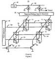
- FIG. 5depicts an embodiment of a memory array 200 using one embodiment of a magnetic memory cell 100 in accordance with the present invention that displays the reading/writing scheme and positioning.
- the memory array 200includes a row selection 210 , a writing column selection 220 and a reading column selection 230 .
- Column selectioncan be split for reading and writing into two components, as indicated in FIG. 5, for convenience and/or ease of depiction. However, nothing prevents the reading and writing column selection from being performed by a single unit.
- Both writing column selection 220 and read column selection 230if split, can be at the same sides, top or bottom of the memory array 200 .
- the row selection 210is coupled to the gates of the transistors 102 of the memory cells 100 via word lines 212 and 214 .
- the reading column selection 230is coupled to the drains of the transistors 102 via read bit lines 232 and 234 .
- the reading column selectionis coupled to an output 236 and a line 240 to a supply voltage Vdd via a load 238 .
- the writing column selection 220is coupled to the magnetic tunneling junctions 104 of the memory cells 100 via write bit lines 222 and 224 .
- the writing column selection 220receives write current Iw 226 during writing. Also depicted are digit lines 202 and 204 , which provide a current for writing to the memory cells in a write mode.
- the row selection 210selects a row for reading by providing a voltage to the gate of the transistor 102 of the selected memory cell 100 via the word line 212 or 214 .
- the writing column selection 220is disabled during reading. Thus, the write current Iw will not be provided to the memory cells 100 during reading.
- the reading column selection 230selects a column to read.
- the reading column selection 230selects a column to read.
- the current through the transistor and the read bit line 232 or 234depends upon the state of the magnetic tunneling junction 104 in the selected cell 100 .
- the output voltageis read on output line 236 .
- the states of the magnetic tunneling junctioncan also be read out by detecting the electric current in the load 238 .
- the transistor 102Because of the arrangement of the transistor 102 and the magnetic tunneling junction 104 in the memory cell 100 , the voltage developed on the output line 236 is relatively large. In particular, as discussed above, the transistor 102 amplifies the signal from the magnetic tunneling junction 104 for output over the output line 236 .
- the reading column selection 230is disabled during writing.
- the writing column selection 220provides a write current which flows through the selected write bit line 222 or 224 to ground.
- the digit line 202 or 204carries current flowing through the digit line 202 or 204 . This current flows substantially perpendicular to the flow of current in the write bit line 222 or 224 .
- the cell residing in the selected write bit line 222 or 224 and the selected digit line 202 or 204is written.
- the direction of flow of the current in the digit line 202 or 204i.e. right to left or left to right as shown in FIG.
- the state of the magnetic tunneling junctionis set to be a low resistance or a high resistance.
- the array 200utilizes the memory cells 100 . In order to do so, the memory array 200 applies a voltage to the gates of the transistors 102 in the selected cell 100 . When read, the current in the transistor 102 and read bit line 232 or 234 depends on the state of the magnetic tunneling junction 104 . Similarly, the output voltage output at line 236 also depends upon the state of the magnetic tunneling junction 104 . Because the memory array 200 can utilize the memory cells 100 , the memory array 200 can provide a larger signal, that is, a larger difference between output signals for different states of the memory cells 100 . Consequently, the memory array 200 is more reliable.
- the memory cell 100 and memory arrays 150 and 200have a larger signal and are more reliable.
- the memory arrays 150 and 200may have simpler circuitry.
- the write currentcan pass through the write bit line to ground without requiring the transistors, such as the transistors 58 and 60 of the conventional memory array in FIG. 2, to provide a bypass for write current.
Landscapes
- Engineering & Computer Science (AREA)
- Computer Hardware Design (AREA)
- Hall/Mr Elements (AREA)
- Mram Or Spin Memory Techniques (AREA)
Abstract
Description
Claims (16)
Priority Applications (1)
| Application Number | Priority Date | Filing Date | Title |
|---|---|---|---|
| US09/990,425US6512690B1 (en) | 2001-08-15 | 2001-11-21 | High sensitivity common source amplifier MRAM cell, memory array and read/write scheme |
Applications Claiming Priority (2)
| Application Number | Priority Date | Filing Date | Title |
|---|---|---|---|
| US31257901P | 2001-08-15 | 2001-08-15 | |
| US09/990,425US6512690B1 (en) | 2001-08-15 | 2001-11-21 | High sensitivity common source amplifier MRAM cell, memory array and read/write scheme |
Publications (1)
| Publication Number | Publication Date |
|---|---|
| US6512690B1true US6512690B1 (en) | 2003-01-28 |
Family
ID=26978459
Family Applications (1)
| Application Number | Title | Priority Date | Filing Date |
|---|---|---|---|
| US09/990,425Expired - LifetimeUS6512690B1 (en) | 2001-08-15 | 2001-11-21 | High sensitivity common source amplifier MRAM cell, memory array and read/write scheme |
Country Status (1)
| Country | Link |
|---|---|
| US (1) | US6512690B1 (en) |
Cited By (147)
| Publication number | Priority date | Publication date | Assignee | Title |
|---|---|---|---|---|
| US6611452B1 (en)* | 2002-04-05 | 2003-08-26 | T-Ram, Inc. | Reference cells for TCCT based memory cells |
| US20040017706A1 (en)* | 2001-01-25 | 2004-01-29 | Martin Freitag | MRAM configuration |
| US6829160B1 (en)* | 2001-04-06 | 2004-12-07 | Western Digital (Fremont), Inc. | Magnetic ram cell with amplification circuitry and MRAM memory array formed using the MRAM cells |
| US20040246776A1 (en)* | 2003-06-06 | 2004-12-09 | Seagate Technology Llc | Magnetic random access memory having flux closure for the free layer and spin transfer write mechanism |
| US6842364B1 (en)* | 2003-07-07 | 2005-01-11 | Hewlett-Packard Development Company, L.P. | Memory cell strings in a resistive cross point memory cell array |
| US20050083731A1 (en)* | 2001-12-21 | 2005-04-21 | Yoshihisa Iwata | Magnetic random access memory |
| US20050135150A1 (en)* | 2003-12-19 | 2005-06-23 | Brandenberger Sarah M. | Magnetic memory storage device |
| US20060067104A1 (en)* | 2004-09-30 | 2006-03-30 | Sharp Laboratories Of America, Inc. | Complementary output resistive memory cell |
| US7095647B1 (en)* | 2002-12-20 | 2006-08-22 | Silicon Magnetic Systems | Magnetic memory array with an improved world line configuration |
| US20070076470A1 (en)* | 2005-09-13 | 2007-04-05 | Northern Lights Semiconductor Corp. | Magnetic Random Access Memory Device and Sensing Method Thereof |
| US7272035B1 (en)* | 2005-08-31 | 2007-09-18 | Grandis, Inc. | Current driven switching of magnetic storage cells utilizing spin transfer and magnetic memories using such cells |
| US7272034B1 (en)* | 2005-08-31 | 2007-09-18 | Grandis, Inc. | Current driven switching of magnetic storage cells utilizing spin transfer and magnetic memories using such cells |
| US20070279970A1 (en)* | 2006-06-02 | 2007-12-06 | Honeywell International Inc. | Nonvolatile memory with data clearing functionality |
| US20100109656A1 (en)* | 2008-10-31 | 2010-05-06 | Seagate Technology Llc | Magnetic Tunnel Junction and Memristor Apparatus |
| US8830628B1 (en) | 2009-02-23 | 2014-09-09 | Western Digital (Fremont), Llc | Method and system for providing a perpendicular magnetic recording head |
| US8879207B1 (en) | 2011-12-20 | 2014-11-04 | Western Digital (Fremont), Llc | Method for providing a side shield for a magnetic recording transducer using an air bridge |
| US8883017B1 (en) | 2013-03-12 | 2014-11-11 | Western Digital (Fremont), Llc | Method and system for providing a read transducer having seamless interfaces |
| US8917581B1 (en) | 2013-12-18 | 2014-12-23 | Western Digital Technologies, Inc. | Self-anneal process for a near field transducer and chimney in a hard disk drive assembly |
| US8923102B1 (en) | 2013-07-16 | 2014-12-30 | Western Digital (Fremont), Llc | Optical grating coupling for interferometric waveguides in heat assisted magnetic recording heads |
| US8947985B1 (en) | 2013-07-16 | 2015-02-03 | Western Digital (Fremont), Llc | Heat assisted magnetic recording transducers having a recessed pole |
| US8953422B1 (en) | 2014-06-10 | 2015-02-10 | Western Digital (Fremont), Llc | Near field transducer using dielectric waveguide core with fine ridge feature |
| US8958272B1 (en) | 2014-06-10 | 2015-02-17 | Western Digital (Fremont), Llc | Interfering near field transducer for energy assisted magnetic recording |
| US8971160B1 (en) | 2013-12-19 | 2015-03-03 | Western Digital (Fremont), Llc | Near field transducer with high refractive index pin for heat assisted magnetic recording |
| US8970988B1 (en) | 2013-12-31 | 2015-03-03 | Western Digital (Fremont), Llc | Electric gaps and method for making electric gaps for multiple sensor arrays |
| US8976635B1 (en) | 2014-06-10 | 2015-03-10 | Western Digital (Fremont), Llc | Near field transducer driven by a transverse electric waveguide for energy assisted magnetic recording |
| US8980109B1 (en) | 2012-12-11 | 2015-03-17 | Western Digital (Fremont), Llc | Method for providing a magnetic recording transducer using a combined main pole and side shield CMP for a wraparound shield scheme |
| US8982508B1 (en) | 2011-10-31 | 2015-03-17 | Western Digital (Fremont), Llc | Method for providing a side shield for a magnetic recording transducer |
| US8988812B1 (en) | 2013-11-27 | 2015-03-24 | Western Digital (Fremont), Llc | Multi-sensor array configuration for a two-dimensional magnetic recording (TDMR) operation |
| US8988825B1 (en) | 2014-02-28 | 2015-03-24 | Western Digital (Fremont, LLC | Method for fabricating a magnetic writer having half-side shields |
| US8984740B1 (en) | 2012-11-30 | 2015-03-24 | Western Digital (Fremont), Llc | Process for providing a magnetic recording transducer having a smooth magnetic seed layer |
| US8995087B1 (en) | 2006-11-29 | 2015-03-31 | Western Digital (Fremont), Llc | Perpendicular magnetic recording write head having a wrap around shield |
| US8993217B1 (en) | 2013-04-04 | 2015-03-31 | Western Digital (Fremont), Llc | Double exposure technique for high resolution disk imaging |
| US9001467B1 (en) | 2014-03-05 | 2015-04-07 | Western Digital (Fremont), Llc | Method for fabricating side shields in a magnetic writer |
| US8997832B1 (en) | 2010-11-23 | 2015-04-07 | Western Digital (Fremont), Llc | Method of fabricating micrometer scale components |
| US9001628B1 (en) | 2013-12-16 | 2015-04-07 | Western Digital (Fremont), Llc | Assistant waveguides for evaluating main waveguide coupling efficiency and diode laser alignment tolerances for hard disk |
| US9007879B1 (en) | 2014-06-10 | 2015-04-14 | Western Digital (Fremont), Llc | Interfering near field transducer having a wide metal bar feature for energy assisted magnetic recording |
| US9007719B1 (en) | 2013-10-23 | 2015-04-14 | Western Digital (Fremont), Llc | Systems and methods for using double mask techniques to achieve very small features |
| US9007725B1 (en) | 2014-10-07 | 2015-04-14 | Western Digital (Fremont), Llc | Sensor with positive coupling between dual ferromagnetic free layer laminates |
| US9013836B1 (en) | 2013-04-02 | 2015-04-21 | Western Digital (Fremont), Llc | Method and system for providing an antiferromagnetically coupled return pole |
| US9042058B1 (en) | 2013-10-17 | 2015-05-26 | Western Digital Technologies, Inc. | Shield designed for middle shields in a multiple sensor array |
| US9042052B1 (en) | 2014-06-23 | 2015-05-26 | Western Digital (Fremont), Llc | Magnetic writer having a partially shunted coil |
| US9042208B1 (en) | 2013-03-11 | 2015-05-26 | Western Digital Technologies, Inc. | Disk drive measuring fly height by applying a bias voltage to an electrically insulated write component of a head |
| US9042057B1 (en) | 2013-01-09 | 2015-05-26 | Western Digital (Fremont), Llc | Methods for providing magnetic storage elements with high magneto-resistance using Heusler alloys |
| US9042051B2 (en) | 2013-08-15 | 2015-05-26 | Western Digital (Fremont), Llc | Gradient write gap for perpendicular magnetic recording writer |
| US9053735B1 (en) | 2014-06-20 | 2015-06-09 | Western Digital (Fremont), Llc | Method for fabricating a magnetic writer using a full-film metal planarization |
| US9064528B1 (en) | 2013-05-17 | 2015-06-23 | Western Digital Technologies, Inc. | Interferometric waveguide usable in shingled heat assisted magnetic recording in the absence of a near-field transducer |
| US9064507B1 (en) | 2009-07-31 | 2015-06-23 | Western Digital (Fremont), Llc | Magnetic etch-stop layer for magnetoresistive read heads |
| US9065043B1 (en) | 2012-06-29 | 2015-06-23 | Western Digital (Fremont), Llc | Tunnel magnetoresistance read head with narrow shield-to-shield spacing |
| US9064527B1 (en) | 2013-04-12 | 2015-06-23 | Western Digital (Fremont), Llc | High order tapered waveguide for use in a heat assisted magnetic recording head |
| US9070381B1 (en) | 2013-04-12 | 2015-06-30 | Western Digital (Fremont), Llc | Magnetic recording read transducer having a laminated free layer |
| US9082423B1 (en) | 2013-12-18 | 2015-07-14 | Western Digital (Fremont), Llc | Magnetic recording write transducer having an improved trailing surface profile |
| US9087527B1 (en) | 2014-10-28 | 2015-07-21 | Western Digital (Fremont), Llc | Apparatus and method for middle shield connection in magnetic recording transducers |
| US9087534B1 (en) | 2011-12-20 | 2015-07-21 | Western Digital (Fremont), Llc | Method and system for providing a read transducer having soft and hard magnetic bias structures |
| US9093639B2 (en) | 2012-02-21 | 2015-07-28 | Western Digital (Fremont), Llc | Methods for manufacturing a magnetoresistive structure utilizing heating and cooling |
| US9104107B1 (en) | 2013-04-03 | 2015-08-11 | Western Digital (Fremont), Llc | DUV photoresist process |
| US9111564B1 (en) | 2013-04-02 | 2015-08-18 | Western Digital (Fremont), Llc | Magnetic recording writer having a main pole with multiple flare angles |
| US9111558B1 (en) | 2014-03-14 | 2015-08-18 | Western Digital (Fremont), Llc | System and method of diffractive focusing of light in a waveguide |
| US9111550B1 (en) | 2014-12-04 | 2015-08-18 | Western Digital (Fremont), Llc | Write transducer having a magnetic buffer layer spaced between a side shield and a write pole by non-magnetic layers |
| US9123374B1 (en) | 2015-02-12 | 2015-09-01 | Western Digital (Fremont), Llc | Heat assisted magnetic recording writer having an integrated polarization rotation plate |
| US9123359B1 (en) | 2010-12-22 | 2015-09-01 | Western Digital (Fremont), Llc | Magnetic recording transducer with sputtered antiferromagnetic coupling trilayer between plated ferromagnetic shields and method of fabrication |
| US9123358B1 (en) | 2012-06-11 | 2015-09-01 | Western Digital (Fremont), Llc | Conformal high moment side shield seed layer for perpendicular magnetic recording writer |
| US9123362B1 (en) | 2011-03-22 | 2015-09-01 | Western Digital (Fremont), Llc | Methods for assembling an electrically assisted magnetic recording (EAMR) head |
| US9135930B1 (en) | 2014-03-06 | 2015-09-15 | Western Digital (Fremont), Llc | Method for fabricating a magnetic write pole using vacuum deposition |
| US9135937B1 (en) | 2014-05-09 | 2015-09-15 | Western Digital (Fremont), Llc | Current modulation on laser diode for energy assisted magnetic recording transducer |
| US9142233B1 (en) | 2014-02-28 | 2015-09-22 | Western Digital (Fremont), Llc | Heat assisted magnetic recording writer having a recessed pole |
| US9147408B1 (en) | 2013-12-19 | 2015-09-29 | Western Digital (Fremont), Llc | Heated AFM layer deposition and cooling process for TMR magnetic recording sensor with high pinning field |
| US9147404B1 (en) | 2015-03-31 | 2015-09-29 | Western Digital (Fremont), Llc | Method and system for providing a read transducer having a dual free layer |
| US9153255B1 (en) | 2014-03-05 | 2015-10-06 | Western Digital (Fremont), Llc | Method for fabricating a magnetic writer having an asymmetric gap and shields |
| US9171589B2 (en) | 2011-12-12 | 2015-10-27 | Samsung Electronics Co., Ltd. | Memory device, method of performing read or write operation and memory system including the same |
| US9183854B2 (en) | 2014-02-24 | 2015-11-10 | Western Digital (Fremont), Llc | Method to make interferometric taper waveguide for HAMR light delivery |
| US9190085B1 (en) | 2014-03-12 | 2015-11-17 | Western Digital (Fremont), Llc | Waveguide with reflective grating for localized energy intensity |
| US9190079B1 (en) | 2014-09-22 | 2015-11-17 | Western Digital (Fremont), Llc | Magnetic write pole having engineered radius of curvature and chisel angle profiles |
| US9194692B1 (en) | 2013-12-06 | 2015-11-24 | Western Digital (Fremont), Llc | Systems and methods for using white light interferometry to measure undercut of a bi-layer structure |
| US9202480B2 (en) | 2009-10-14 | 2015-12-01 | Western Digital (Fremont), LLC. | Double patterning hard mask for damascene perpendicular magnetic recording (PMR) writer |
| US9202493B1 (en) | 2014-02-28 | 2015-12-01 | Western Digital (Fremont), Llc | Method of making an ultra-sharp tip mode converter for a HAMR head |
| US9213322B1 (en) | 2012-08-16 | 2015-12-15 | Western Digital (Fremont), Llc | Methods for providing run to run process control using a dynamic tuner |
| US9214169B1 (en) | 2014-06-20 | 2015-12-15 | Western Digital (Fremont), Llc | Magnetic recording read transducer having a laminated free layer |
| US9214172B2 (en) | 2013-10-23 | 2015-12-15 | Western Digital (Fremont), Llc | Method of manufacturing a magnetic read head |
| US9214165B1 (en) | 2014-12-18 | 2015-12-15 | Western Digital (Fremont), Llc | Magnetic writer having a gradient in saturation magnetization of the shields |
| US9230565B1 (en) | 2014-06-24 | 2016-01-05 | Western Digital (Fremont), Llc | Magnetic shield for magnetic recording head |
| US9236560B1 (en) | 2014-12-08 | 2016-01-12 | Western Digital (Fremont), Llc | Spin transfer torque tunneling magnetoresistive device having a laminated free layer with perpendicular magnetic anisotropy |
| US9245545B1 (en) | 2013-04-12 | 2016-01-26 | Wester Digital (Fremont), Llc | Short yoke length coils for magnetic heads in disk drives |
| US9245562B1 (en) | 2015-03-30 | 2016-01-26 | Western Digital (Fremont), Llc | Magnetic recording writer with a composite main pole |
| US9245543B1 (en) | 2010-06-25 | 2016-01-26 | Western Digital (Fremont), Llc | Method for providing an energy assisted magnetic recording head having a laser integrally mounted to the slider |
| US9251813B1 (en) | 2009-04-19 | 2016-02-02 | Western Digital (Fremont), Llc | Method of making a magnetic recording head |
| US9263067B1 (en) | 2013-05-29 | 2016-02-16 | Western Digital (Fremont), Llc | Process for making PMR writer with constant side wall angle |
| US9263071B1 (en) | 2015-03-31 | 2016-02-16 | Western Digital (Fremont), Llc | Flat NFT for heat assisted magnetic recording |
| US9269382B1 (en) | 2012-06-29 | 2016-02-23 | Western Digital (Fremont), Llc | Method and system for providing a read transducer having improved pinning of the pinned layer at higher recording densities |
| US9275657B1 (en) | 2013-08-14 | 2016-03-01 | Western Digital (Fremont), Llc | Process for making PMR writer with non-conformal side gaps |
| US9280990B1 (en) | 2013-12-11 | 2016-03-08 | Western Digital (Fremont), Llc | Method for fabricating a magnetic writer using multiple etches |
| US9286919B1 (en) | 2014-12-17 | 2016-03-15 | Western Digital (Fremont), Llc | Magnetic writer having a dual side gap |
| US9287494B1 (en) | 2013-06-28 | 2016-03-15 | Western Digital (Fremont), Llc | Magnetic tunnel junction (MTJ) with a magnesium oxide tunnel barrier |
| US9305583B1 (en) | 2014-02-18 | 2016-04-05 | Western Digital (Fremont), Llc | Method for fabricating a magnetic writer using multiple etches of damascene materials |
| US9312064B1 (en) | 2015-03-02 | 2016-04-12 | Western Digital (Fremont), Llc | Method to fabricate a magnetic head including ion milling of read gap using dual layer hard mask |
| US9318130B1 (en) | 2013-07-02 | 2016-04-19 | Western Digital (Fremont), Llc | Method to fabricate tunneling magnetic recording heads with extended pinned layer |
| US9336814B1 (en) | 2013-03-12 | 2016-05-10 | Western Digital (Fremont), Llc | Inverse tapered waveguide for use in a heat assisted magnetic recording head |
| US9343086B1 (en) | 2013-09-11 | 2016-05-17 | Western Digital (Fremont), Llc | Magnetic recording write transducer having an improved sidewall angle profile |
| US9343098B1 (en) | 2013-08-23 | 2016-05-17 | Western Digital (Fremont), Llc | Method for providing a heat assisted magnetic recording transducer having protective pads |
| US9343087B1 (en) | 2014-12-21 | 2016-05-17 | Western Digital (Fremont), Llc | Method for fabricating a magnetic writer having half shields |
| US9349394B1 (en) | 2013-10-18 | 2016-05-24 | Western Digital (Fremont), Llc | Method for fabricating a magnetic writer having a gradient side gap |
| US9349392B1 (en) | 2012-05-24 | 2016-05-24 | Western Digital (Fremont), Llc | Methods for improving adhesion on dielectric substrates |
| US9361914B1 (en) | 2014-06-18 | 2016-06-07 | Western Digital (Fremont), Llc | Magnetic sensor with thin capping layer |
| US9361913B1 (en) | 2013-06-03 | 2016-06-07 | Western Digital (Fremont), Llc | Recording read heads with a multi-layer AFM layer methods and apparatuses |
| US9368134B1 (en) | 2010-12-16 | 2016-06-14 | Western Digital (Fremont), Llc | Method and system for providing an antiferromagnetically coupled writer |
| US9384763B1 (en) | 2015-03-26 | 2016-07-05 | Western Digital (Fremont), Llc | Dual free layer magnetic reader having a rear bias structure including a soft bias layer |
| US9384765B1 (en) | 2015-09-24 | 2016-07-05 | Western Digital (Fremont), Llc | Method and system for providing a HAMR writer having improved optical efficiency |
| US9396742B1 (en) | 2012-11-30 | 2016-07-19 | Western Digital (Fremont), Llc | Magnetoresistive sensor for a magnetic storage system read head, and fabrication method thereof |
| US9396743B1 (en) | 2014-02-28 | 2016-07-19 | Western Digital (Fremont), Llc | Systems and methods for controlling soft bias thickness for tunnel magnetoresistance readers |
| US9406331B1 (en) | 2013-06-17 | 2016-08-02 | Western Digital (Fremont), Llc | Method for making ultra-narrow read sensor and read transducer device resulting therefrom |
| US9424866B1 (en) | 2015-09-24 | 2016-08-23 | Western Digital (Fremont), Llc | Heat assisted magnetic recording write apparatus having a dielectric gap |
| US9431032B1 (en) | 2013-08-14 | 2016-08-30 | Western Digital (Fremont), Llc | Electrical connection arrangement for a multiple sensor array usable in two-dimensional magnetic recording |
| US9431031B1 (en) | 2015-03-24 | 2016-08-30 | Western Digital (Fremont), Llc | System and method for magnetic transducers having multiple sensors and AFC shields |
| US9431038B1 (en) | 2015-06-29 | 2016-08-30 | Western Digital (Fremont), Llc | Method for fabricating a magnetic write pole having an improved sidewall angle profile |
| US9431047B1 (en) | 2013-05-01 | 2016-08-30 | Western Digital (Fremont), Llc | Method for providing an improved AFM reader shield |
| US9431039B1 (en) | 2013-05-21 | 2016-08-30 | Western Digital (Fremont), Llc | Multiple sensor array usable in two-dimensional magnetic recording |
| US9437251B1 (en) | 2014-12-22 | 2016-09-06 | Western Digital (Fremont), Llc | Apparatus and method having TDMR reader to reader shunts |
| US9443541B1 (en) | 2015-03-24 | 2016-09-13 | Western Digital (Fremont), Llc | Magnetic writer having a gradient in saturation magnetization of the shields and return pole |
| US9441938B1 (en) | 2013-10-08 | 2016-09-13 | Western Digital (Fremont), Llc | Test structures for measuring near field transducer disc length |
| US9449625B1 (en) | 2014-12-24 | 2016-09-20 | Western Digital (Fremont), Llc | Heat assisted magnetic recording head having a plurality of diffusion barrier layers |
| US9449621B1 (en) | 2015-03-26 | 2016-09-20 | Western Digital (Fremont), Llc | Dual free layer magnetic reader having a rear bias structure having a high aspect ratio |
| US9472216B1 (en) | 2015-09-23 | 2016-10-18 | Western Digital (Fremont), Llc | Differential dual free layer magnetic reader |
| TWI555018B (en)* | 2011-12-22 | 2016-10-21 | 科羅庫斯科技股份有限公司 | Method of writing to a self-referenced mram cell |
| US9484051B1 (en) | 2015-11-09 | 2016-11-01 | The Provost, Fellows, Foundation Scholars and the other members of Board, of the College of the Holy and Undivided Trinity of Queen Elizabeth near Dublin | Method and system for reducing undesirable reflections in a HAMR write apparatus |
| US9508363B1 (en) | 2014-06-17 | 2016-11-29 | Western Digital (Fremont), Llc | Method for fabricating a magnetic write pole having a leading edge bevel |
| US9508372B1 (en) | 2015-06-03 | 2016-11-29 | Western Digital (Fremont), Llc | Shingle magnetic writer having a low sidewall angle pole |
| US9508365B1 (en) | 2015-06-24 | 2016-11-29 | Western Digital (Fremont), LLC. | Magnetic reader having a crystal decoupling structure |
| US9530443B1 (en) | 2015-06-25 | 2016-12-27 | Western Digital (Fremont), Llc | Method for fabricating a magnetic recording device having a high aspect ratio structure |
| US9564150B1 (en) | 2015-11-24 | 2017-02-07 | Western Digital (Fremont), Llc | Magnetic read apparatus having an improved read sensor isolation circuit |
| US9595273B1 (en) | 2015-09-30 | 2017-03-14 | Western Digital (Fremont), Llc | Shingle magnetic writer having nonconformal shields |
| US9646639B2 (en) | 2015-06-26 | 2017-05-09 | Western Digital (Fremont), Llc | Heat assisted magnetic recording writer having integrated polarization rotation waveguides |
| US9666214B1 (en) | 2015-09-23 | 2017-05-30 | Western Digital (Fremont), Llc | Free layer magnetic reader that may have a reduced shield-to-shield spacing |
| US9721595B1 (en) | 2014-12-04 | 2017-08-01 | Western Digital (Fremont), Llc | Method for providing a storage device |
| US9741366B1 (en) | 2014-12-18 | 2017-08-22 | Western Digital (Fremont), Llc | Method for fabricating a magnetic writer having a gradient in saturation magnetization of the shields |
| US9740805B1 (en) | 2015-12-01 | 2017-08-22 | Western Digital (Fremont), Llc | Method and system for detecting hotspots for photolithographically-defined devices |
| US9754611B1 (en) | 2015-11-30 | 2017-09-05 | Western Digital (Fremont), Llc | Magnetic recording write apparatus having a stepped conformal trailing shield |
| US9767831B1 (en) | 2015-12-01 | 2017-09-19 | Western Digital (Fremont), Llc | Magnetic writer having convex trailing surface pole and conformal write gap |
| US9786301B1 (en) | 2014-12-02 | 2017-10-10 | Western Digital (Fremont), Llc | Apparatuses and methods for providing thin shields in a multiple sensor array |
| US9799351B1 (en) | 2015-11-30 | 2017-10-24 | Western Digital (Fremont), Llc | Short yoke length writer having assist coils |
| US9812155B1 (en) | 2015-11-23 | 2017-11-07 | Western Digital (Fremont), Llc | Method and system for fabricating high junction angle read sensors |
| US9842615B1 (en) | 2015-06-26 | 2017-12-12 | Western Digital (Fremont), Llc | Magnetic reader having a nonmagnetic insertion layer for the pinning layer |
| US9858951B1 (en) | 2015-12-01 | 2018-01-02 | Western Digital (Fremont), Llc | Method for providing a multilayer AFM layer in a read sensor |
| US9881638B1 (en) | 2014-12-17 | 2018-01-30 | Western Digital (Fremont), Llc | Method for providing a near-field transducer (NFT) for a heat assisted magnetic recording (HAMR) device |
| US9934811B1 (en) | 2014-03-07 | 2018-04-03 | Western Digital (Fremont), Llc | Methods for controlling stray fields of magnetic features using magneto-elastic anisotropy |
| US9953670B1 (en) | 2015-11-10 | 2018-04-24 | Western Digital (Fremont), Llc | Method and system for providing a HAMR writer including a multi-mode interference device |
| US10037770B1 (en) | 2015-11-12 | 2018-07-31 | Western Digital (Fremont), Llc | Method for providing a magnetic recording write apparatus having a seamless pole |
| US10074387B1 (en) | 2014-12-21 | 2018-09-11 | Western Digital (Fremont), Llc | Method and system for providing a read transducer having symmetric antiferromagnetically coupled shields |
| TWI732603B (en)* | 2019-06-25 | 2021-07-01 | 台灣積體電路製造股份有限公司 | Mram memory cell and method for forming mram memory cell |
Citations (3)
| Publication number | Priority date | Publication date | Assignee | Title |
|---|---|---|---|---|
| US6275411B1 (en)* | 1993-07-23 | 2001-08-14 | Nonvolatile Electronics, Incorporated | Spin dependent tunneling memory |
| US6304477B1 (en)* | 2001-01-31 | 2001-10-16 | Motorola, Inc. | Content addressable magnetic random access memory |
| US6324093B1 (en)* | 2000-09-15 | 2001-11-27 | Hewlett-Packard Company | Write-once thin-film memory |
- 2001
- 2001-11-21USUS09/990,425patent/US6512690B1/ennot_activeExpired - Lifetime
Patent Citations (3)
| Publication number | Priority date | Publication date | Assignee | Title |
|---|---|---|---|---|
| US6275411B1 (en)* | 1993-07-23 | 2001-08-14 | Nonvolatile Electronics, Incorporated | Spin dependent tunneling memory |
| US6324093B1 (en)* | 2000-09-15 | 2001-11-27 | Hewlett-Packard Company | Write-once thin-film memory |
| US6304477B1 (en)* | 2001-01-31 | 2001-10-16 | Motorola, Inc. | Content addressable magnetic random access memory |
Cited By (177)
| Publication number | Priority date | Publication date | Assignee | Title |
|---|---|---|---|---|
| US20040017706A1 (en)* | 2001-01-25 | 2004-01-29 | Martin Freitag | MRAM configuration |
| US6791871B2 (en)* | 2001-01-25 | 2004-09-14 | Infineon Technologies Ag | MRAM configuration |
| US6829160B1 (en)* | 2001-04-06 | 2004-12-07 | Western Digital (Fremont), Inc. | Magnetic ram cell with amplification circuitry and MRAM memory array formed using the MRAM cells |
| US20050083731A1 (en)* | 2001-12-21 | 2005-04-21 | Yoshihisa Iwata | Magnetic random access memory |
| US6990004B2 (en)* | 2001-12-21 | 2006-01-24 | Kabushiki Kaisha Toshiba | Magnetic random access memory |
| US6611452B1 (en)* | 2002-04-05 | 2003-08-26 | T-Ram, Inc. | Reference cells for TCCT based memory cells |
| US6845037B1 (en) | 2002-04-05 | 2005-01-18 | T-Ram, Inc. | Reference cells for TCCT based memory cells |
| US7095647B1 (en)* | 2002-12-20 | 2006-08-22 | Silicon Magnetic Systems | Magnetic memory array with an improved world line configuration |
| US6865109B2 (en) | 2003-06-06 | 2005-03-08 | Seagate Technology Llc | Magnetic random access memory having flux closure for the free layer and spin transfer write mechanism |
| US20040246776A1 (en)* | 2003-06-06 | 2004-12-09 | Seagate Technology Llc | Magnetic random access memory having flux closure for the free layer and spin transfer write mechanism |
| US20050007825A1 (en)* | 2003-07-07 | 2005-01-13 | Hilton Richard Lee | Memory cell strings in a resistive cross point memory cell array |
| US6842364B1 (en)* | 2003-07-07 | 2005-01-11 | Hewlett-Packard Development Company, L.P. | Memory cell strings in a resistive cross point memory cell array |
| US20050135150A1 (en)* | 2003-12-19 | 2005-06-23 | Brandenberger Sarah M. | Magnetic memory storage device |
| US7038941B2 (en) | 2003-12-19 | 2006-05-02 | Hewlett-Packard Development Company, L.P. | Magnetic memory storage device |
| US7339813B2 (en)* | 2004-09-30 | 2008-03-04 | Sharp Laboratories Of America, Inc. | Complementary output resistive memory cell |
| US20060067104A1 (en)* | 2004-09-30 | 2006-03-30 | Sharp Laboratories Of America, Inc. | Complementary output resistive memory cell |
| US7272035B1 (en)* | 2005-08-31 | 2007-09-18 | Grandis, Inc. | Current driven switching of magnetic storage cells utilizing spin transfer and magnetic memories using such cells |
| US7272034B1 (en)* | 2005-08-31 | 2007-09-18 | Grandis, Inc. | Current driven switching of magnetic storage cells utilizing spin transfer and magnetic memories using such cells |
| US20070076470A1 (en)* | 2005-09-13 | 2007-04-05 | Northern Lights Semiconductor Corp. | Magnetic Random Access Memory Device and Sensing Method Thereof |
| US7499313B2 (en)* | 2006-06-02 | 2009-03-03 | Honeywell International Inc. | Nonvolatile memory with data clearing functionality |
| US20070279970A1 (en)* | 2006-06-02 | 2007-12-06 | Honeywell International Inc. | Nonvolatile memory with data clearing functionality |
| US8995087B1 (en) | 2006-11-29 | 2015-03-31 | Western Digital (Fremont), Llc | Perpendicular magnetic recording write head having a wrap around shield |
| US20100109656A1 (en)* | 2008-10-31 | 2010-05-06 | Seagate Technology Llc | Magnetic Tunnel Junction and Memristor Apparatus |
| US7898844B2 (en)* | 2008-10-31 | 2011-03-01 | Seagate Technology, Llc | Magnetic tunnel junction and memristor apparatus |
| US20120014175A1 (en)* | 2008-10-31 | 2012-01-19 | Seagate Technology Llc | Magnetic Tunnel Junction and Memristor Apparatus |
| US8391055B2 (en)* | 2008-10-31 | 2013-03-05 | Seagate Technology Llc | Magnetic tunnel junction and memristor apparatus |
| US8830628B1 (en) | 2009-02-23 | 2014-09-09 | Western Digital (Fremont), Llc | Method and system for providing a perpendicular magnetic recording head |
| US9251813B1 (en) | 2009-04-19 | 2016-02-02 | Western Digital (Fremont), Llc | Method of making a magnetic recording head |
| US9064507B1 (en) | 2009-07-31 | 2015-06-23 | Western Digital (Fremont), Llc | Magnetic etch-stop layer for magnetoresistive read heads |
| US9202480B2 (en) | 2009-10-14 | 2015-12-01 | Western Digital (Fremont), LLC. | Double patterning hard mask for damascene perpendicular magnetic recording (PMR) writer |
| US9245543B1 (en) | 2010-06-25 | 2016-01-26 | Western Digital (Fremont), Llc | Method for providing an energy assisted magnetic recording head having a laser integrally mounted to the slider |
| US9672847B2 (en) | 2010-11-23 | 2017-06-06 | Western Digital (Fremont), Llc | Micrometer scale components |
| US9159345B1 (en) | 2010-11-23 | 2015-10-13 | Western Digital (Fremont), Llc | Micrometer scale components |
| US8997832B1 (en) | 2010-11-23 | 2015-04-07 | Western Digital (Fremont), Llc | Method of fabricating micrometer scale components |
| US9368134B1 (en) | 2010-12-16 | 2016-06-14 | Western Digital (Fremont), Llc | Method and system for providing an antiferromagnetically coupled writer |
| US9123359B1 (en) | 2010-12-22 | 2015-09-01 | Western Digital (Fremont), Llc | Magnetic recording transducer with sputtered antiferromagnetic coupling trilayer between plated ferromagnetic shields and method of fabrication |
| US9123362B1 (en) | 2011-03-22 | 2015-09-01 | Western Digital (Fremont), Llc | Methods for assembling an electrically assisted magnetic recording (EAMR) head |
| US8982508B1 (en) | 2011-10-31 | 2015-03-17 | Western Digital (Fremont), Llc | Method for providing a side shield for a magnetic recording transducer |
| US9171589B2 (en) | 2011-12-12 | 2015-10-27 | Samsung Electronics Co., Ltd. | Memory device, method of performing read or write operation and memory system including the same |
| US9087534B1 (en) | 2011-12-20 | 2015-07-21 | Western Digital (Fremont), Llc | Method and system for providing a read transducer having soft and hard magnetic bias structures |
| US8879207B1 (en) | 2011-12-20 | 2014-11-04 | Western Digital (Fremont), Llc | Method for providing a side shield for a magnetic recording transducer using an air bridge |
| TWI555018B (en)* | 2011-12-22 | 2016-10-21 | 科羅庫斯科技股份有限公司 | Method of writing to a self-referenced mram cell |
| US9093639B2 (en) | 2012-02-21 | 2015-07-28 | Western Digital (Fremont), Llc | Methods for manufacturing a magnetoresistive structure utilizing heating and cooling |
| US9349392B1 (en) | 2012-05-24 | 2016-05-24 | Western Digital (Fremont), Llc | Methods for improving adhesion on dielectric substrates |
| US9940950B2 (en) | 2012-05-24 | 2018-04-10 | Western Digital (Fremont), Llc | Methods for improving adhesion on dielectric substrates |
| US9123358B1 (en) | 2012-06-11 | 2015-09-01 | Western Digital (Fremont), Llc | Conformal high moment side shield seed layer for perpendicular magnetic recording writer |
| US9065043B1 (en) | 2012-06-29 | 2015-06-23 | Western Digital (Fremont), Llc | Tunnel magnetoresistance read head with narrow shield-to-shield spacing |
| US9269382B1 (en) | 2012-06-29 | 2016-02-23 | Western Digital (Fremont), Llc | Method and system for providing a read transducer having improved pinning of the pinned layer at higher recording densities |
| US9412400B2 (en) | 2012-06-29 | 2016-08-09 | Western Digital (Fremont), Llc | Tunnel magnetoresistance read head with narrow shield-to-shield spacing |
| US9213322B1 (en) | 2012-08-16 | 2015-12-15 | Western Digital (Fremont), Llc | Methods for providing run to run process control using a dynamic tuner |
| US9396742B1 (en) | 2012-11-30 | 2016-07-19 | Western Digital (Fremont), Llc | Magnetoresistive sensor for a magnetic storage system read head, and fabrication method thereof |
| US8984740B1 (en) | 2012-11-30 | 2015-03-24 | Western Digital (Fremont), Llc | Process for providing a magnetic recording transducer having a smooth magnetic seed layer |
| US8980109B1 (en) | 2012-12-11 | 2015-03-17 | Western Digital (Fremont), Llc | Method for providing a magnetic recording transducer using a combined main pole and side shield CMP for a wraparound shield scheme |
| US9042057B1 (en) | 2013-01-09 | 2015-05-26 | Western Digital (Fremont), Llc | Methods for providing magnetic storage elements with high magneto-resistance using Heusler alloys |
| US9042208B1 (en) | 2013-03-11 | 2015-05-26 | Western Digital Technologies, Inc. | Disk drive measuring fly height by applying a bias voltage to an electrically insulated write component of a head |
| US9336814B1 (en) | 2013-03-12 | 2016-05-10 | Western Digital (Fremont), Llc | Inverse tapered waveguide for use in a heat assisted magnetic recording head |
| US8883017B1 (en) | 2013-03-12 | 2014-11-11 | Western Digital (Fremont), Llc | Method and system for providing a read transducer having seamless interfaces |
| US9013836B1 (en) | 2013-04-02 | 2015-04-21 | Western Digital (Fremont), Llc | Method and system for providing an antiferromagnetically coupled return pole |
| US9111564B1 (en) | 2013-04-02 | 2015-08-18 | Western Digital (Fremont), Llc | Magnetic recording writer having a main pole with multiple flare angles |
| US9104107B1 (en) | 2013-04-03 | 2015-08-11 | Western Digital (Fremont), Llc | DUV photoresist process |
| US8993217B1 (en) | 2013-04-04 | 2015-03-31 | Western Digital (Fremont), Llc | Double exposure technique for high resolution disk imaging |
| US9064527B1 (en) | 2013-04-12 | 2015-06-23 | Western Digital (Fremont), Llc | High order tapered waveguide for use in a heat assisted magnetic recording head |
| US9070381B1 (en) | 2013-04-12 | 2015-06-30 | Western Digital (Fremont), Llc | Magnetic recording read transducer having a laminated free layer |
| US9245545B1 (en) | 2013-04-12 | 2016-01-26 | Wester Digital (Fremont), Llc | Short yoke length coils for magnetic heads in disk drives |
| US9431047B1 (en) | 2013-05-01 | 2016-08-30 | Western Digital (Fremont), Llc | Method for providing an improved AFM reader shield |
| US9064528B1 (en) | 2013-05-17 | 2015-06-23 | Western Digital Technologies, Inc. | Interferometric waveguide usable in shingled heat assisted magnetic recording in the absence of a near-field transducer |
| US9431039B1 (en) | 2013-05-21 | 2016-08-30 | Western Digital (Fremont), Llc | Multiple sensor array usable in two-dimensional magnetic recording |
| US9263067B1 (en) | 2013-05-29 | 2016-02-16 | Western Digital (Fremont), Llc | Process for making PMR writer with constant side wall angle |
| US9361913B1 (en) | 2013-06-03 | 2016-06-07 | Western Digital (Fremont), Llc | Recording read heads with a multi-layer AFM layer methods and apparatuses |
| US9406331B1 (en) | 2013-06-17 | 2016-08-02 | Western Digital (Fremont), Llc | Method for making ultra-narrow read sensor and read transducer device resulting therefrom |
| US9287494B1 (en) | 2013-06-28 | 2016-03-15 | Western Digital (Fremont), Llc | Magnetic tunnel junction (MTJ) with a magnesium oxide tunnel barrier |
| US9318130B1 (en) | 2013-07-02 | 2016-04-19 | Western Digital (Fremont), Llc | Method to fabricate tunneling magnetic recording heads with extended pinned layer |
| US8923102B1 (en) | 2013-07-16 | 2014-12-30 | Western Digital (Fremont), Llc | Optical grating coupling for interferometric waveguides in heat assisted magnetic recording heads |
| US8947985B1 (en) | 2013-07-16 | 2015-02-03 | Western Digital (Fremont), Llc | Heat assisted magnetic recording transducers having a recessed pole |
| US9431032B1 (en) | 2013-08-14 | 2016-08-30 | Western Digital (Fremont), Llc | Electrical connection arrangement for a multiple sensor array usable in two-dimensional magnetic recording |
| US9275657B1 (en) | 2013-08-14 | 2016-03-01 | Western Digital (Fremont), Llc | Process for making PMR writer with non-conformal side gaps |
| US9042051B2 (en) | 2013-08-15 | 2015-05-26 | Western Digital (Fremont), Llc | Gradient write gap for perpendicular magnetic recording writer |
| US9343098B1 (en) | 2013-08-23 | 2016-05-17 | Western Digital (Fremont), Llc | Method for providing a heat assisted magnetic recording transducer having protective pads |
| US9343086B1 (en) | 2013-09-11 | 2016-05-17 | Western Digital (Fremont), Llc | Magnetic recording write transducer having an improved sidewall angle profile |
| US9441938B1 (en) | 2013-10-08 | 2016-09-13 | Western Digital (Fremont), Llc | Test structures for measuring near field transducer disc length |
| US9042058B1 (en) | 2013-10-17 | 2015-05-26 | Western Digital Technologies, Inc. | Shield designed for middle shields in a multiple sensor array |
| US9349394B1 (en) | 2013-10-18 | 2016-05-24 | Western Digital (Fremont), Llc | Method for fabricating a magnetic writer having a gradient side gap |
| US9214172B2 (en) | 2013-10-23 | 2015-12-15 | Western Digital (Fremont), Llc | Method of manufacturing a magnetic read head |
| US9007719B1 (en) | 2013-10-23 | 2015-04-14 | Western Digital (Fremont), Llc | Systems and methods for using double mask techniques to achieve very small features |
| US9830936B2 (en) | 2013-10-23 | 2017-11-28 | Western Digital (Fremont), Llc | Magnetic read head with antiferromagentic layer |
| US8988812B1 (en) | 2013-11-27 | 2015-03-24 | Western Digital (Fremont), Llc | Multi-sensor array configuration for a two-dimensional magnetic recording (TDMR) operation |
| US9194692B1 (en) | 2013-12-06 | 2015-11-24 | Western Digital (Fremont), Llc | Systems and methods for using white light interferometry to measure undercut of a bi-layer structure |
| US9280990B1 (en) | 2013-12-11 | 2016-03-08 | Western Digital (Fremont), Llc | Method for fabricating a magnetic writer using multiple etches |
| US9001628B1 (en) | 2013-12-16 | 2015-04-07 | Western Digital (Fremont), Llc | Assistant waveguides for evaluating main waveguide coupling efficiency and diode laser alignment tolerances for hard disk |
| US8917581B1 (en) | 2013-12-18 | 2014-12-23 | Western Digital Technologies, Inc. | Self-anneal process for a near field transducer and chimney in a hard disk drive assembly |
| US9082423B1 (en) | 2013-12-18 | 2015-07-14 | Western Digital (Fremont), Llc | Magnetic recording write transducer having an improved trailing surface profile |
| US8971160B1 (en) | 2013-12-19 | 2015-03-03 | Western Digital (Fremont), Llc | Near field transducer with high refractive index pin for heat assisted magnetic recording |
| US9147408B1 (en) | 2013-12-19 | 2015-09-29 | Western Digital (Fremont), Llc | Heated AFM layer deposition and cooling process for TMR magnetic recording sensor with high pinning field |
| US8970988B1 (en) | 2013-12-31 | 2015-03-03 | Western Digital (Fremont), Llc | Electric gaps and method for making electric gaps for multiple sensor arrays |
| US9305583B1 (en) | 2014-02-18 | 2016-04-05 | Western Digital (Fremont), Llc | Method for fabricating a magnetic writer using multiple etches of damascene materials |
| US9183854B2 (en) | 2014-02-24 | 2015-11-10 | Western Digital (Fremont), Llc | Method to make interferometric taper waveguide for HAMR light delivery |
| US9202493B1 (en) | 2014-02-28 | 2015-12-01 | Western Digital (Fremont), Llc | Method of making an ultra-sharp tip mode converter for a HAMR head |
| US9396743B1 (en) | 2014-02-28 | 2016-07-19 | Western Digital (Fremont), Llc | Systems and methods for controlling soft bias thickness for tunnel magnetoresistance readers |
| US9142233B1 (en) | 2014-02-28 | 2015-09-22 | Western Digital (Fremont), Llc | Heat assisted magnetic recording writer having a recessed pole |
| US8988825B1 (en) | 2014-02-28 | 2015-03-24 | Western Digital (Fremont, LLC | Method for fabricating a magnetic writer having half-side shields |
| US9153255B1 (en) | 2014-03-05 | 2015-10-06 | Western Digital (Fremont), Llc | Method for fabricating a magnetic writer having an asymmetric gap and shields |
| US9349393B2 (en) | 2014-03-05 | 2016-05-24 | Western Digital (Fremont), Llc | Magnetic writer having an asymmetric gap and shields |
| US9001467B1 (en) | 2014-03-05 | 2015-04-07 | Western Digital (Fremont), Llc | Method for fabricating side shields in a magnetic writer |
| US9135930B1 (en) | 2014-03-06 | 2015-09-15 | Western Digital (Fremont), Llc | Method for fabricating a magnetic write pole using vacuum deposition |
| US9934811B1 (en) | 2014-03-07 | 2018-04-03 | Western Digital (Fremont), Llc | Methods for controlling stray fields of magnetic features using magneto-elastic anisotropy |
| US9495984B2 (en) | 2014-03-12 | 2016-11-15 | Western Digital (Fremont), Llc | Waveguide with reflective grating for localized energy intensity |
| US9190085B1 (en) | 2014-03-12 | 2015-11-17 | Western Digital (Fremont), Llc | Waveguide with reflective grating for localized energy intensity |
| US9111558B1 (en) | 2014-03-14 | 2015-08-18 | Western Digital (Fremont), Llc | System and method of diffractive focusing of light in a waveguide |
| US9135937B1 (en) | 2014-05-09 | 2015-09-15 | Western Digital (Fremont), Llc | Current modulation on laser diode for energy assisted magnetic recording transducer |
| US9007879B1 (en) | 2014-06-10 | 2015-04-14 | Western Digital (Fremont), Llc | Interfering near field transducer having a wide metal bar feature for energy assisted magnetic recording |
| US9159346B1 (en) | 2014-06-10 | 2015-10-13 | Western Digital (Fremont), Llc | Near field transducer using dielectric waveguide core with fine ridge feature |
| US9311952B2 (en) | 2014-06-10 | 2016-04-12 | Western Digital (Fremont), Llc | Interfering near field transducer for energy assisted magnetic recording |
| US8953422B1 (en) | 2014-06-10 | 2015-02-10 | Western Digital (Fremont), Llc | Near field transducer using dielectric waveguide core with fine ridge feature |
| US8976635B1 (en) | 2014-06-10 | 2015-03-10 | Western Digital (Fremont), Llc | Near field transducer driven by a transverse electric waveguide for energy assisted magnetic recording |
| US8958272B1 (en) | 2014-06-10 | 2015-02-17 | Western Digital (Fremont), Llc | Interfering near field transducer for energy assisted magnetic recording |
| US9508363B1 (en) | 2014-06-17 | 2016-11-29 | Western Digital (Fremont), Llc | Method for fabricating a magnetic write pole having a leading edge bevel |
| US9361914B1 (en) | 2014-06-18 | 2016-06-07 | Western Digital (Fremont), Llc | Magnetic sensor with thin capping layer |
| US9214169B1 (en) | 2014-06-20 | 2015-12-15 | Western Digital (Fremont), Llc | Magnetic recording read transducer having a laminated free layer |
| US9053735B1 (en) | 2014-06-20 | 2015-06-09 | Western Digital (Fremont), Llc | Method for fabricating a magnetic writer using a full-film metal planarization |
| US9042052B1 (en) | 2014-06-23 | 2015-05-26 | Western Digital (Fremont), Llc | Magnetic writer having a partially shunted coil |
| US9230565B1 (en) | 2014-06-24 | 2016-01-05 | Western Digital (Fremont), Llc | Magnetic shield for magnetic recording head |
| US9190079B1 (en) | 2014-09-22 | 2015-11-17 | Western Digital (Fremont), Llc | Magnetic write pole having engineered radius of curvature and chisel angle profiles |
| US9007725B1 (en) | 2014-10-07 | 2015-04-14 | Western Digital (Fremont), Llc | Sensor with positive coupling between dual ferromagnetic free layer laminates |
| US9087527B1 (en) | 2014-10-28 | 2015-07-21 | Western Digital (Fremont), Llc | Apparatus and method for middle shield connection in magnetic recording transducers |
| US9786301B1 (en) | 2014-12-02 | 2017-10-10 | Western Digital (Fremont), Llc | Apparatuses and methods for providing thin shields in a multiple sensor array |
| US9721595B1 (en) | 2014-12-04 | 2017-08-01 | Western Digital (Fremont), Llc | Method for providing a storage device |
| US9111550B1 (en) | 2014-12-04 | 2015-08-18 | Western Digital (Fremont), Llc | Write transducer having a magnetic buffer layer spaced between a side shield and a write pole by non-magnetic layers |
| US9705072B2 (en) | 2014-12-08 | 2017-07-11 | Western Digital (Fremont), Llc | Spin transfer torque tunneling magnetoresistive device having a laminated free layer with perpendicular magnetic anisotropy |
| US9236560B1 (en) | 2014-12-08 | 2016-01-12 | Western Digital (Fremont), Llc | Spin transfer torque tunneling magnetoresistive device having a laminated free layer with perpendicular magnetic anisotropy |
| US9881638B1 (en) | 2014-12-17 | 2018-01-30 | Western Digital (Fremont), Llc | Method for providing a near-field transducer (NFT) for a heat assisted magnetic recording (HAMR) device |
| US10553241B2 (en) | 2014-12-17 | 2020-02-04 | Western Digital Technologies, Inc. | Near-field transducer (NFT) for a heat assisted magnetic recording (HAMR) device |
| US9286919B1 (en) | 2014-12-17 | 2016-03-15 | Western Digital (Fremont), Llc | Magnetic writer having a dual side gap |
| US9214165B1 (en) | 2014-12-18 | 2015-12-15 | Western Digital (Fremont), Llc | Magnetic writer having a gradient in saturation magnetization of the shields |
| US9741366B1 (en) | 2014-12-18 | 2017-08-22 | Western Digital (Fremont), Llc | Method for fabricating a magnetic writer having a gradient in saturation magnetization of the shields |
| US10074387B1 (en) | 2014-12-21 | 2018-09-11 | Western Digital (Fremont), Llc | Method and system for providing a read transducer having symmetric antiferromagnetically coupled shields |
| US9343087B1 (en) | 2014-12-21 | 2016-05-17 | Western Digital (Fremont), Llc | Method for fabricating a magnetic writer having half shields |
| US9437251B1 (en) | 2014-12-22 | 2016-09-06 | Western Digital (Fremont), Llc | Apparatus and method having TDMR reader to reader shunts |
| US9449625B1 (en) | 2014-12-24 | 2016-09-20 | Western Digital (Fremont), Llc | Heat assisted magnetic recording head having a plurality of diffusion barrier layers |
| US9123374B1 (en) | 2015-02-12 | 2015-09-01 | Western Digital (Fremont), Llc | Heat assisted magnetic recording writer having an integrated polarization rotation plate |
| US9312064B1 (en) | 2015-03-02 | 2016-04-12 | Western Digital (Fremont), Llc | Method to fabricate a magnetic head including ion milling of read gap using dual layer hard mask |
| US9443541B1 (en) | 2015-03-24 | 2016-09-13 | Western Digital (Fremont), Llc | Magnetic writer having a gradient in saturation magnetization of the shields and return pole |
| US9431031B1 (en) | 2015-03-24 | 2016-08-30 | Western Digital (Fremont), Llc | System and method for magnetic transducers having multiple sensors and AFC shields |
| US9449621B1 (en) | 2015-03-26 | 2016-09-20 | Western Digital (Fremont), Llc | Dual free layer magnetic reader having a rear bias structure having a high aspect ratio |
| US9922672B1 (en) | 2015-03-26 | 2018-03-20 | Western Digital (Fremont), Llc | Dual free layer magnetic reader having a rear bias structure having a high aspect ratio |
| US9384763B1 (en) | 2015-03-26 | 2016-07-05 | Western Digital (Fremont), Llc | Dual free layer magnetic reader having a rear bias structure including a soft bias layer |
| US9245562B1 (en) | 2015-03-30 | 2016-01-26 | Western Digital (Fremont), Llc | Magnetic recording writer with a composite main pole |
| US9263071B1 (en) | 2015-03-31 | 2016-02-16 | Western Digital (Fremont), Llc | Flat NFT for heat assisted magnetic recording |
| US9147404B1 (en) | 2015-03-31 | 2015-09-29 | Western Digital (Fremont), Llc | Method and system for providing a read transducer having a dual free layer |
| US9508372B1 (en) | 2015-06-03 | 2016-11-29 | Western Digital (Fremont), Llc | Shingle magnetic writer having a low sidewall angle pole |
| US9508365B1 (en) | 2015-06-24 | 2016-11-29 | Western Digital (Fremont), LLC. | Magnetic reader having a crystal decoupling structure |
| US9530443B1 (en) | 2015-06-25 | 2016-12-27 | Western Digital (Fremont), Llc | Method for fabricating a magnetic recording device having a high aspect ratio structure |
| US9646639B2 (en) | 2015-06-26 | 2017-05-09 | Western Digital (Fremont), Llc | Heat assisted magnetic recording writer having integrated polarization rotation waveguides |
| US9842615B1 (en) | 2015-06-26 | 2017-12-12 | Western Digital (Fremont), Llc | Magnetic reader having a nonmagnetic insertion layer for the pinning layer |
| US10242700B2 (en) | 2015-06-26 | 2019-03-26 | Western Digital (Fremont), Llc | Magnetic reader having a nonmagnetic insertion layer for the pinning layer |
| US9431038B1 (en) | 2015-06-29 | 2016-08-30 | Western Digital (Fremont), Llc | Method for fabricating a magnetic write pole having an improved sidewall angle profile |
| US9472216B1 (en) | 2015-09-23 | 2016-10-18 | Western Digital (Fremont), Llc | Differential dual free layer magnetic reader |
| US9666214B1 (en) | 2015-09-23 | 2017-05-30 | Western Digital (Fremont), Llc | Free layer magnetic reader that may have a reduced shield-to-shield spacing |
| US9384765B1 (en) | 2015-09-24 | 2016-07-05 | Western Digital (Fremont), Llc | Method and system for providing a HAMR writer having improved optical efficiency |
| US9424866B1 (en) | 2015-09-24 | 2016-08-23 | Western Digital (Fremont), Llc | Heat assisted magnetic recording write apparatus having a dielectric gap |
| US9595273B1 (en) | 2015-09-30 | 2017-03-14 | Western Digital (Fremont), Llc | Shingle magnetic writer having nonconformal shields |
| US9484051B1 (en) | 2015-11-09 | 2016-11-01 | The Provost, Fellows, Foundation Scholars and the other members of Board, of the College of the Holy and Undivided Trinity of Queen Elizabeth near Dublin | Method and system for reducing undesirable reflections in a HAMR write apparatus |
| US9953670B1 (en) | 2015-11-10 | 2018-04-24 | Western Digital (Fremont), Llc | Method and system for providing a HAMR writer including a multi-mode interference device |
| US10381029B2 (en) | 2015-11-10 | 2019-08-13 | Western Digital (Fremont), Llc | Method and system for providing a HAMR writer including a multi-mode interference device |
| US10037770B1 (en) | 2015-11-12 | 2018-07-31 | Western Digital (Fremont), Llc | Method for providing a magnetic recording write apparatus having a seamless pole |
| US9812155B1 (en) | 2015-11-23 | 2017-11-07 | Western Digital (Fremont), Llc | Method and system for fabricating high junction angle read sensors |
| US9564150B1 (en) | 2015-11-24 | 2017-02-07 | Western Digital (Fremont), Llc | Magnetic read apparatus having an improved read sensor isolation circuit |
| US9799351B1 (en) | 2015-11-30 | 2017-10-24 | Western Digital (Fremont), Llc | Short yoke length writer having assist coils |
| US10121495B2 (en) | 2015-11-30 | 2018-11-06 | Western Digital (Fremont), Llc | Magnetic recording write apparatus having a stepped conformal trailing shield |
| US9754611B1 (en) | 2015-11-30 | 2017-09-05 | Western Digital (Fremont), Llc | Magnetic recording write apparatus having a stepped conformal trailing shield |
| US9740805B1 (en) | 2015-12-01 | 2017-08-22 | Western Digital (Fremont), Llc | Method and system for detecting hotspots for photolithographically-defined devices |
| US9997177B2 (en) | 2015-12-01 | 2018-06-12 | Western Digital (Fremont), Llc | Magnetic writer having convex trailing surface pole and conformal write gap |
| US9858951B1 (en) | 2015-12-01 | 2018-01-02 | Western Digital (Fremont), Llc | Method for providing a multilayer AFM layer in a read sensor |
| US9767831B1 (en) | 2015-12-01 | 2017-09-19 | Western Digital (Fremont), Llc | Magnetic writer having convex trailing surface pole and conformal write gap |
| TWI732603B (en)* | 2019-06-25 | 2021-07-01 | 台灣積體電路製造股份有限公司 | Mram memory cell and method for forming mram memory cell |
| US11244983B2 (en) | 2019-06-25 | 2022-02-08 | Taiwan Semiconductor Manufacturing Co., Ltd. | MRAM memory cell layout for minimizing bitcell area |
| US11800724B2 (en) | 2019-06-25 | 2023-10-24 | Taiwan Semiconductor Manufacturing Co., Ltd. | MRAM memory cell layout for minimizing bitcell area |
| US12279437B2 (en) | 2019-06-25 | 2025-04-15 | Taiwan Semiconductor Manufacturing Co., Ltd. | MRAM memory cell layout for minimizing bitcell area |
Similar Documents
| Publication | Publication Date | Title |
|---|---|---|
| US6512690B1 (en) | High sensitivity common source amplifier MRAM cell, memory array and read/write scheme | |
| US6829160B1 (en) | Magnetic ram cell with amplification circuitry and MRAM memory array formed using the MRAM cells | |
| US8320166B2 (en) | Magnetic random access memory and method of reading data from the same | |
| US6614681B2 (en) | Thin film magnetic memory device with memory cells including a tunnel magnetic resistive element | |
| US7272035B1 (en) | Current driven switching of magnetic storage cells utilizing spin transfer and magnetic memories using such cells | |
| US7272034B1 (en) | Current driven switching of magnetic storage cells utilizing spin transfer and magnetic memories using such cells | |
| JP3800925B2 (en) | Magnetic random access memory circuit | |
| US6678189B2 (en) | Method and system for performing equipotential sensing across a memory array to eliminate leakage currents | |
| EP1302948B1 (en) | Memory sense amplifier | |
| US6462981B2 (en) | Magnetic random access memory | |
| JP4046513B2 (en) | Semiconductor integrated circuit | |
| US6982909B2 (en) | System and method for reading a memory cell | |
| US6781873B2 (en) | Non-volatile memory device capable of generating accurate reference current for determination | |
| JP5135609B2 (en) | Semiconductor device | |
| US6836422B1 (en) | System and method for reading a memory cell | |
| US6975555B2 (en) | Magnetic random access memory using memory cells with rotated magnetic storage elements | |
| US6958933B2 (en) | Memory cell strings | |
| US6865108B2 (en) | Memory cell strings in a resistive cross point memory cell array | |
| JP3427974B2 (en) | Magnetic random access memory circuit | |
| KR100516691B1 (en) | Magnetoresistive RAM |
Legal Events
| Date | Code | Title | Description |
|---|---|---|---|
| AS | Assignment | Owner name:READ-RITE CORPORATION, CALIFORNIA Free format text:ASSIGNMENT OF ASSIGNORS INTEREST;ASSIGNORS:QI, QIUQUN (KEVIN);SHI, XIZENG;REEL/FRAME:012321/0826 Effective date:20011115 | |
| AS | Assignment | Owner name:TENNENBAUM CAPITAL PARTNERS, LLC, CALIFORNIA Free format text:SECURITY INTEREST;ASSIGNOR:READ-RITE CORPORATION;REEL/FRAME:013616/0399 Effective date:20021224 | |
| STCF | Information on status: patent grant | Free format text:PATENTED CASE | |
| AS | Assignment | Owner name:WESTERN DIGITAL (FREMONT), INC., CALIFORNIA Free format text:ASSIGNMENT OF ASSIGNORS INTEREST;ASSIGNOR:READ-RITE CORPORATION;REEL/FRAME:014506/0765 Effective date:20030731 | |
| AS | Assignment | Owner name:READ-RITE CORPORATION, CALIFORNIA Free format text:RELEASE OF SECURITY INTEREST;ASSIGNOR:TENNENBAUM CAPITAL PARTNERS, LLC;REEL/FRAME:014499/0476 Effective date:20030731 | |
| AS | Assignment | Owner name:GENERAL ELECTRIC CAPITAL CORPORATION, AS AGENT, CA Free format text:SECURITY INTEREST;ASSIGNORS:WESTERN DIGITAL TECHNOLOGIES, INC.;WESTERN DIGITAL (FREMONT), INC.;REEL/FRAME:014830/0957 Effective date:20030919 | |
| FPAY | Fee payment | Year of fee payment:4 | |
| AS | Assignment | Owner name:WESTERN DIGITAL (FREMONT), INC., CALIFORNIA Free format text:RELEASE BY SECURED PARTY;ASSIGNOR:GENERAL ELECTRIC CAPITAL CORPORATION, AS AGENT;REEL/FRAME:020599/0489 Effective date:20070809 Owner name:WESTERN DIGITAL TECHNOLOGIES, INC., CALIFORNIA Free format text:RELEASE BY SECURED PARTY;ASSIGNOR:GENERAL ELECTRIC CAPITAL CORPORATION, AS AGENT;REEL/FRAME:020599/0489 Effective date:20070809 | |
| FPAY | Fee payment | Year of fee payment:8 | |
| REMI | Maintenance fee reminder mailed | ||
| FPAY | Fee payment | Year of fee payment:12 | |
| SULP | Surcharge for late payment | Year of fee payment:11 | |
| AS | Assignment | Owner name:JPMORGAN CHASE BANK, N.A., AS COLLATERAL AGENT, IL Free format text:SECURITY AGREEMENT;ASSIGNOR:WESTERN DIGITAL (FREMONT), LLC;REEL/FRAME:038710/0845 Effective date:20160512 Owner name:JPMORGAN CHASE BANK, N.A., AS COLLATERAL AGENT, IL Free format text:SECURITY AGREEMENT;ASSIGNOR:WESTERN DIGITAL (FREMONT), LLC;REEL/FRAME:038744/0755 Effective date:20160512 Owner name:U.S. BANK NATIONAL ASSOCIATION, AS COLLATERAL AGEN Free format text:SECURITY AGREEMENT;ASSIGNOR:WESTERN DIGITAL (FREMONT), LLC;REEL/FRAME:038744/0675 Effective date:20160512 | |
| AS | Assignment | Owner name:WESTERN DIGITAL (FREMONT), LLC, CALIFORNIA Free format text:RELEASE BY SECURED PARTY;ASSIGNOR:U.S. BANK NATIONAL ASSOCIATION, AS COLLATERAL AGENT;REEL/FRAME:045501/0158 Effective date:20180227 | |
| AS | Assignment | Owner name:WESTERN DIGITAL (FREMONT), LLC, CALIFORNIA Free format text:ENTITY CONVERSION FROM INC TO LLC;ASSIGNOR:WESTERN DIGITAL (FREMONT), INC;REEL/FRAME:048501/0925 Effective date:20070629 | |
| AS | Assignment | Owner name:WESTERN DIGITAL TECHNOLOGIES, INC., CALIFORNIA Free format text:ASSIGNMENT OF ASSIGNORS INTEREST;ASSIGNOR:WESTERN DIGITAL (FREMONT), LLC;REEL/FRAME:050450/0582 Effective date:20190508 | |
| AS | Assignment | Owner name:WESTERN DIGITAL TECHNOLOGIES, INC., CALIFORNIA Free format text:RELEASE OF SECURITY INTEREST AT REEL 038710 FRAME 0845;ASSIGNOR:JPMORGAN CHASE BANK, N.A.;REEL/FRAME:058965/0445 Effective date:20220203 Owner name:WESTERN DIGITAL (FREMONT), LLC, CALIFORNIA Free format text:RELEASE OF SECURITY INTEREST AT REEL 038710 FRAME 0845;ASSIGNOR:JPMORGAN CHASE BANK, N.A.;REEL/FRAME:058965/0445 Effective date:20220203 |