US6512381B2 - Enhanced fingerprint detection - Google Patents
Enhanced fingerprint detectionDownload PDFInfo
- Publication number
- US6512381B2 US6512381B2US09/753,344US75334400AUS6512381B2US 6512381 B2US6512381 B2US 6512381B2US 75334400 AUS75334400 AUS 75334400AUS 6512381 B2US6512381 B2US 6512381B2
- Authority
- US
- United States
- Prior art keywords
- fingerprint
- plate
- voltage
- finger
- capacitor
- Prior art date
- Legal status (The legal status is an assumption and is not a legal conclusion. Google has not performed a legal analysis and makes no representation as to the accuracy of the status listed.)
- Expired - Lifetime
Links
Images


Classifications
- A—HUMAN NECESSITIES
- A61—MEDICAL OR VETERINARY SCIENCE; HYGIENE
- A61B—DIAGNOSIS; SURGERY; IDENTIFICATION
- A61B5/00—Measuring for diagnostic purposes; Identification of persons
- A61B5/117—Identification of persons
- A61B5/1171—Identification of persons based on the shapes or appearances of their bodies or parts thereof
- A61B5/1172—Identification of persons based on the shapes or appearances of their bodies or parts thereof using fingerprinting
- G—PHYSICS
- G01—MEASURING; TESTING
- G01B—MEASURING LENGTH, THICKNESS OR SIMILAR LINEAR DIMENSIONS; MEASURING ANGLES; MEASURING AREAS; MEASURING IRREGULARITIES OF SURFACES OR CONTOURS
- G01B7/00—Measuring arrangements characterised by the use of electric or magnetic techniques
- G01B7/28—Measuring arrangements characterised by the use of electric or magnetic techniques for measuring contours or curvatures
- G01B7/287—Measuring arrangements characterised by the use of electric or magnetic techniques for measuring contours or curvatures using a plurality of fixed, simultaneously operating transducers
- G—PHYSICS
- G06—COMPUTING OR CALCULATING; COUNTING
- G06V—IMAGE OR VIDEO RECOGNITION OR UNDERSTANDING
- G06V40/00—Recognition of biometric, human-related or animal-related patterns in image or video data
- G06V40/10—Human or animal bodies, e.g. vehicle occupants or pedestrians; Body parts, e.g. hands
- G06V40/12—Fingerprints or palmprints
- G06V40/13—Sensors therefor
- G06V40/1306—Sensors therefor non-optical, e.g. ultrasonic or capacitive sensing
Definitions
- This inventionis related to fingerprint pattern recognition, and more particularly, to enhanced fingerprint pattern sensing circuit and method.
- Capacitive sensors to detect a fingerprint patternare currently well known. There are a number of patents which describe capacitive sensors for determining the pattern of ridges and valleys in a person's fingerprint.
- U.S. Pat. No. 4,353,056describes a capacitive fingerprint sensor which has a sensing surface for receiving a fingerprint and sensing the ridges and valleys of the skin using an array of small capacitors.
- U.S. Pat. No. 5,325,442also describes a fingerprint sensing and recognition circuit using a plurality of capacitors arranged in rows and columns.
- Some capacitive sensorsoperate using two or more plates in silicon with a negative feedback as shown in FIGS. 1 and 2, taken from U.S. Pat. No. 5,973,623.
- the finger of the userchanges the capacitance that exists between the two plates in silicon.
- a negative feedback circuitis used in the detection of whether a ridge or a valley is present in the fingerprint.
- FIGS. 3 and 4are prior art. Figures from this patent illustrate a single capacitive plate 14 and a switching device 16 to access the sensor cell. The finger of the user provides the other plate of the capacitor. The value of the capacitor is then sensed to determine the presence of a ridge or a valley.
- One of the problems with the prior art capacitive fingerprint sensorsis their level of sensitivity to distinguish a ridge from a valley.
- the difficulty of obtaining a good fingerprint pattern through capacitive sensingcan vary from individual to individual. With some persons, depending upon their skin characteristics the pattern can be much more difficult to obtain than from other persons. It is therefore preferred to have an enhanced method of capacitive sensing which provides more uniform sensitivity from one individual to another.
- a capacitive fingerprint sensing devicewhich places a variable voltage on the body of the individual whose fingerprint pattern is being sensed.
- the fingeris thus performing the dual function of providing the variable charge transfer during input while also providing the variable capacitance to be sensed.
- the effect of performing both functionseffectively multiplies the measurable effects of having a ridge or a valley at each sensor cell.
- the sensingis significantly enhanced in recognizing and distinguishing the difference between a ridge and a valley.
- the electrical connection to the person's bodycan be made by any number of acceptable techniques.
- an electrical contactis provided to the person's finger while it is placed on the fingerprint sensor pad.
- a logic control circuit connected to the electrical conductorplaces a step voltage on the electrical conductor according to a preset timing sequence in conjunction with the timing of the sensing.
- the voltage changeis placed on the person's body by a capacitive transfer.
- a large plate capacitor in the siliconprovides one plate to transfer charge to the finger to provide the change in voltage while the sensing occurs.
- the voltage changecan be coupled to the body of the user either via another finger or some other appendage.
- the connectorcan be in contact with the other hand of the person, their arm or any other acceptable portion of the body since all that is required is to place a change in charge on the person's body in order to obtain the enhanced capacitive sensing capability.
- the inventioncan be used with sensor cells of the type having one capacitive plate in silicon and the finger providing the other plate, or with the type using multiple capacitor plates in silicon and the finger being a conductor that modifies their relative capacitance.
- the fingerprint or sensor circuitincludes a negative feedback amplifier having the two plates of a feedback capacitor in silicon with a field therebetween.
- the field between the two platesis varied by the user's finger, whether ridge or valley.
- the effect of having a valleyis that the sense capacitance will be greater than in the case of having a ridge.
- the feedback capacitanceis reduced, as compared to a valley.
- the input capacitancewill decrease with the greater distance of the skin from the sensor, such as is present at a valley.
- FIG. 1is a schematic representation of a fingerprint sensor according to the prior art.
- FIG. 2is an electrical schematic representation of an individual cell of the fingerprint sensor of FIG. 1 according to the prior art.
- FIG. 3is a schematic representation of a fingerprint sensor circuit according to different prior art embodiment.
- FIG. 4is an electrical schematic of a fingerprint sensor cell as used in the prior art of FIG. 3 .
- FIG. 5is an electrical schematic of a fingerprint sensor according to principles of the present invention.
- FIG. 6is a schematic representation of a fingerprint sensor according to principles of the present invention.
- FIG. 7is an electrical schematic of an alternative embodiment of a fingerprint sensor according to principles of the present invention.
- FIG. 8Ais an electrical schematic of fingerprint sensor cells for aid in understanding the present invention.
- FIG. 8Bis an electrical schematic of fingerprint sensor cells illustrating one embodiment of the invention.
- FIG. 9is an electrical schematic of a plurality of cells while sensing a fingerprint ridge and valley pattern according to an embodiment of the present invention.
- FIG. 10is an electrical equivalent circuit showing the electrical interaction between various equivalent electrical components according to principles of the present invention.
- FIG. 11is a top view of a housing containing a sensor according to the present invention.
- FIG. 12is a partial cross-sectional view of the substrate of FIG. 11 taken along the lines 12 — 12 .
- FIG. 13is a partial cross-sectional view of a substrate and housing containing the invention.
- FIG. 14is a partial cross-sectional view of an alternative substrate and housing of the present invention.
- FIGS. 15A and 15Bare side views of a further alternative embodiments to place a voltage change on the finger of the user.
- FIGS. 16A and 16Billustrate alternative interference mechanisms which may increase the difficulty of properly reading a fingerprint of a user.
- FIG. 17is an electrical schematic of the circuit according to principles of the present invention.
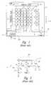
- FIG. 1illustrates a substrate 1 having a plurality of sensor cells 2 thereon.
- the sensor cells 2are in the form of an array 3 and organized to sense a fingerprint pattern of a finger which is placed on top of the substrate.
- the array 3is driven by horizontal scan electronics 5 and also by vertical scan electronics 6 so that each individual cell 2 is selected on a known timing sequence under control of the controller 7 .
- each sensor cell 2includes electronics for sensing the presence or absence of a ridge or a valley of a fingerprint pattern for a finger which is placed on top of the substrate 1 .
- the controller 7includes a power supply circuit 120 which receives power from a power source 95 .
- Each sensing cell 2provides an output on line 17 of each individual column. The output is provided on the chip bus 9 which is provided to an output amplifier 8 and provided to the output of the sensor array 3 at terminal 10 .
- the output of the sensor array 3 at terminal 10is provided to fingerprint pattern recognition electronics which organizes the signal into a fingerprint pattern and compares it to other fingerprint patterns to perform recognition of the fingerprint pattern which is placed thereon.
- the specific details of the array 3 and interaction between the controller 7 to provide fingerprint pattern recognitionis described in U.S. Pat. No. 5,973,623, which is incorporated herein by reference.
- the fingerprint pattern recognitionmay also be obtained and performed by any acceptable technique as described in many other patents and publications which are available to those of skill in the art today.
- FIG. 2illustrates the electronics of a single sensor cell 2 which is acceptable for use in sensing the presence or absence of a ridge or valley according to the prior art.
- the cell shown in FIG. 2is of the type that has two plates in the semiconductor substrate for each cell and the finger provides a third plate to modify the capacitance value of the existing capacitor. It can be considered a three plate cell, two plates in the substrate and one above.
- the specific electronics for the cell 2are provided as only one example by which the cell can be constructed. Other acceptable techniques may also be used since the electronics of the individual cell are provided as an example only.
- the cell 2includes a dielectric layer 11 onto which a person's finger is placed.
- the dielectric layer 11has a top surface 125 which comes in direct contact with the person's finger 18 .
- the finger 18will have a ridge or a valley at the position in which it comes in contact with the cell 2 , the example shown for FIG. 2 including having a ridge thereon so that it is pressed against the substrate 11 and in contact with surface 125 .
- the dielectric layer 11has a thickness D as shown in FIG. 2 .
- a capacitor having plates 24 and 23is against the back surface of the dielectric layer 11 .
- the input plate of the cell 24is connected to the input terminal of an inverting amplifier 13 and the output plate 23 is connected to the output of the inverting amplifier 13 .
- a reset switch 19is closed when sensing is not being performed to reset the inverting amplifier 13 to a known state.
- a capacitor 20provides a step voltage N as applied through V ref at terminal 21 .
- the capacitor C inis of a known value to provide a known charge to the input node 16 of inverting amplifier 13 .
- FIGS. 3 and 4illustrates another acceptable sensor array 3 and cell 2 which may be modified to use the present invention.
- the particular sensor cell 2is known from prior art U.S. Pat. No. 5,325,442, to Knapp, which is hereby incorporated herein by reference.
- the sensor cell of the '442 patent to Knappto include a row driver 100 and a sensor circuit 102 .
- the cell 2 of FIGS. 3 and 4is of the type having one plate in the semiconductor substrate for each cell and the finger provides the second plate to form the capacitor with two plates.
- the row driver circuitcouples to a row conductor 104 to the gate of an access transistor 106 .
- One capacitor plate 108 in the substrateacts as a sense electrode.
- a finger 18provides the other plate of the capacitor ⁇ and the presence of a ridge or valley is determined based on the distance between the plate 108 and plate 18 that form the capacitor.
- the capacitance of the individual capacitorsvaries as a function of the spacing between the finger and the sense plate 108 . The larger capacitance occurs where the finger ridge is adjacent and very close to the plate 108 and the smaller capacitances occurring where a valley is adjacent the plate 108 , but spaced further from the plate because it is a valley.
- the capacitive fingerprint sensorwhether the three plate cell of FIG. 2 or the two plate cell of FIG. 4, operates on the principle that the amount of charge stored on a capacitor is proportional to the voltage multiplied by the capacitance.
- the capacitance value of a capacitorvaries with the distance of the plates from each other.
- the fingerprintwhether a ridge or a valley, acts as a plate of the capacitor.
- the distancevaries in the fingerprint, small for a ridge and large for a valley, the capacitance is also different.
- the capacitance valuealso varies depending upon the fringing effect between the two capacitor plates in the substrate as described by the later equations herein.
- the value of the charge stored or the rate of charge storedcan be measured and sensed in one embodiment, if desired. This is done in some devices by placing a current or voltage on the capacitor and obtaining a measurement corresponding to the stored charge.
- a variation on this methodis to measure a change in output voltage based on a change of charge on the capacitor.
- V outis the output voltage from the cell 2 and q is the charge, and C is the capacitive value.
- ⁇ V outequals the change in voltage on terminal 17
- ⁇ qequals the change in charge on the capacitance
- C sis the capacitance being sensed, namely, the capacitance of the capacitor plates in the sensor with the finger 18 adjacent thereto, whether a ridge or a valley.
- the presence of a ridge and a valleywill cause a variation in the changes in the capacitance.
- the presence of a ridge or a valley near sensor cell 2will cause the capacitance being sensed to be reduced or increased, respectively, so that a ridge and a valley can be distinguished.
- FIGS. 5, 6 and 7illustrate, respectively, alternate embodiments according to the present invention.
- a dielectric layer 11is positioned over a sensor cell 2 .
- a finger 18 of a useris positioned for sensing the fingerprint pattern.
- fingerprintincludes the variations in skin texture on any body part of a person, such as a thumb, a toe, a foot, a forehead, or any other surface whose variations are being sensed to identify a person.
- the finger 18has a ridge directly over the sensor cell 2 . Accordingly, the finger appears as a single flat member against the substrate 11 .
- a sensor cell 2will be smaller than the width of a ridge it will appear, from the view of the cell 2 , that the finger 18 is abutting against the top surface of the dielectric layer 11 .
- FIGS. 8A, 8 B, 9 , 15 A and 15 Ba plurality of different sensor cells 2 are shown to illustrate the response of the array to different parts of the fingerprint, whether a ridge or a valley.
- FIGS. 8A and 8BThe operation of the circuit of FIG. 5 is illustrated schematically in FIGS. 8A and 8B, as will now be explained.
- the circuit of FIGS. 6 and 7is illustrated schematically in FIGS. 9 and 10 and they will be discussed in more detail with respect to these two figures.
- FIGS. 8A and 8Billustrate the sensing principles to illustrate the present invention using a sensor cell of the type generally shown in FIG. 5 .
- FIG. 8Ashows a two plate capacitor system for each cell, the finger 18 being one plate and the plate 14 being the sensor electrode and other plate. Two cells are shown, one at a ridge and the other at a valley.
- C pis the parasitic capacitance affecting the cell output.
- C pthe parasitic capacitance affecting the cell output.
- C pthe parasitic capacitance affecting the cell output.
- C pthe parasitic capacitance C p can sometimes be quite large. Depending on the particular circuit design C p may be much larger than C s . In some cases it may be over ten times larger. If C p is too large, then it will dominate the equation such that changes in C s cause only a very small change in the overall capacitance being sensed as can be seen by viewing equations (2) and (4) together. Accordingly, if the parasitic capacitance is much, much larger than the capacitance being sensed, then the sensitivity of cell 2 is reduced. In most applications, the capacitance being sensed is extremely small since it is based on detecting merely the difference in capacitance value between a ridge and a valley in a single fingerprint.
- the sensitivity of the sensorcan be defined based on the ability to distinguish between the maximum signal output and the minimum signal output.
- ⁇ V outmaxis the highest possible output voltage
- ⁇ V outminis the lowest possible output voltage during a measurement. The sensitivity thus increases with a larger difference between the maximum and minimum changes in output voltages and by reducing the minimum change in output voltage to the lowest possible value.
- the output voltagewill be different from cell 1 to cell 2 based on the difference between C plate ridge and C plate valley . All other aspects of the cells will be the same. Thus, both cells will have the same C in value and the same C p value.
- ⁇ V inis the change in input voltage during sensing
- C inis the input capacitor
- C pis the parasitic capacitor
- C plate bodyis the capacitance that is composed of the plate 14 and the body 18 .
- C incan be carefully controlled and can be reduced to a very low value so as to be negligible, approaching zero.
- C pwill be over 10 times greater than C plate valley , may be up to 20 to 100 times greater.
- C pis difficult to reduce to zero, so we assume C p equals 10 ⁇ C plate valley .
- the sensitivityis reduced to the plate sensitivity ⁇ plate , divided by 11.
- the effect of C pthus causes a significant reduction in sensitivity.
- the sensitivitywill reduce even further.
- FIG. 8Billustrates one embodiment of the present invention showing how applying V in to the body can increase the sensitivity and reduce the effects of C p .
- the step voltage ⁇ V inis applied to the finger 18 and the body acts as capacitor C in .
- the value of C inwill be different for each cell, depending on whether a valley or a ridge is present over the cell.
- a ridgethe value C in will be higher for a ridge and lower for a valley.
- the capacitance change caused by ridge or valley being presentcan be effectively considered as multiplying the change in output since it affects both the input signal and the sense signal.
- C plate ridgeis larger than C plate valley by a value ⁇ C plate ridge and that ⁇ plate is defined as ⁇ ⁇ ⁇ C plate ⁇ ⁇ ridge C plate ⁇ ⁇ valley ,
- Equation (21)shows that C p is in both the numerator and denominator.
- the effect of C pwill be to cancel itself out, towards a value equal to 1 in the equation.
- C pbecomes large, the result will be to cancel out its effect on the sensitivity since it is in both top and bottom in the ratio.
- Equation (25)shows that the invention results in a 5-times improvement in sensitivity for the invention applied to the simple case of FIG. 8 B.
- FIG. 5shows a circuit of a single cell that takes advantage of the principles of the invention that have just been shown in the example of FIG. 8B.
- a select transistor 112coupled to a plate 14 having a finger 18 thereon provides an output V out .
- a voltage terminal 21 having a step voltage input signal V inis connected to the finger 18 .
- FIG. 6illustrates another example of fingerprint sensing according to principles of the present invention.
- the sensor cell as shown in FIG. 6is a further example that provides even more remarkable results than the single plate sensor cell of FIG. 5 as explained herein as will be clear from the technical discussion.
- an electrical conductor 21is connected to the body of the person whose fingerprint is being sensed. It may be coupled at any convenient location, such as the finger itself whose print is being sensed, the hand of the user, the unused hand of the user, the foot, via a conductive foot pad, or other location. Electrical conductor 21 has a terminal 99 connected to a variable voltage supply ⁇ V in .
- the ⁇ V inis directly controlled in a timing sequence with electronic controller 7 to place a known change of voltage on the body and thus on the finger 18 in conjunction with the timing of sensing in each individual cell 2 .
- the ⁇ V inwill normally be a low value and, once sensing has begun will undergo step voltage to high value as shown by the signal wave 114 applied to the terminal ⁇ V in .
- the cell 2will be reset and the electrical conductor 21 will be returned to a low value so as to place the both the cell and the body in a reset mode in preparation for the next sensing cycle at which time ⁇ V in undergoes another step value upwards as shown by signal wave 114 in FIG. 4 .
- the step on ⁇ V inis timed in conjunction with the timing sequence of a clock signal ⁇ r which controls the opening and closing of switch 19 . Namely, switch 19 is opened and after which the ⁇ V in undergoes the step function upwards so that the change in voltage ⁇ V in occurs when switch 19 is open. This creates a change on input node 25 to inverting amplifier 13 which creates a change in voltage on V out corresponding to ⁇ V out as discussed in the prior equations.
- the three plate capacitor system of FIGS. 2, 6 , 7 , 9 , and 10causes a change in the output voltage by two effects, the plate effect, already discussed, and the fringing effect between the two plates 23 and 24 .
- the fringing effectthe presence of a ridge will greatly reduce the fringe capacitive between plates 23 and 24 , whereas a valley will cause little or no reduction. Having a conductor adjacent the plates of the capacitor will ground some of the field lines between the capacitance plates.
- the sensed capacitance Cswill be greater than that of a ridge since a valley has a conductor spaced farther from the cell 2 .
- the reduction of capacitancemay be zero though, in a real sense, even a valley may cause some slight reduction in the capacitance value.
- the general principleapplies for a multiple plate capacitive sensor that Cs will be larger with a greater distance of the finger 18 from the cell such as occurs at a valley and Cs will decrease with the finger closer to the cell such as occurs at a ridge. Namely, the sensed plate capacitance Cs for a valley is greater than for a ridge.
- ⁇ fringeis the idealized sensitivity between plates 23 and 24 for the fringe capacitor.
- FIG. 6in which the invention is used to apply the input voltage to the body.
- FIGS. 7, 9 and 10A further embodiment of a circuit is shown in FIG. 7, and theoretical schematics are shown in FIGS. 9 and 10.
- an additional compensation voltage ⁇ V cis applied to a filter capacitor C f with the voltage ⁇ V c being opposite the wave form ⁇ V in .
- the grain G of amplifier 13is finite and, as shown in FIG. 10, there are parasite capacitors C p on the input and output nodes to the amplifier 13 .
- ⁇ ⁇ ⁇ V out⁇ ⁇ ⁇ V in ⁇ C plate ⁇ ⁇ body G + 1 G ⁇ C fringebody + C platebody + C p G ( 40 )
- the inventionthus has the affect, in the non-ideal case of canceling out completely the parasitic capacitance as well as increasing the sensitivity as the gain G of amplifier 13 goes higher.
- FIG. 7illustrates an alternative embodiment for a circuit according to principles of the present invention. Now that the mathematical calculations have been shown, the circuit of FIG. 7 will be described in more detail. Namely, the circuit of FIG. 7 is different from FIG. 6 in that a separate capacitor C f is present on the input 25 . This separate capacitor C f acts as a compensation capacitor or filter to the input node 25 to enhance and further increase the sensitivity. One plate of the capacitor C f is connected to the sense node 25 whereas the other plate of the capacitor is connected to a voltage source V c representing a compensation voltage. The voltage source V c also undergoes a change in voltage according to a known timing sequence and thus is shown as a ⁇ V c .
- the compensation voltage ⁇ V cundergoes a change in voltage which is exactly opposite that of ⁇ V in which is placed on the body.
- the signals ⁇ V in and ⁇ V cwill normally be the inverse of each other such that when ⁇ V in undergoes a step function up, ⁇ V c will undergo step down.
- the magnitude and absolute direction of ⁇ V in and ⁇ V cis not critical; a change in voltage of some magnitude is desired. Namely, the ⁇ V in shown in FIG.
- ⁇ V incan transition from low to high and from high to low, respectively, as shown in FIG. 7 or can transition from high to low and from low to high, respectively, in order to provide the enhanced sensing according to principles of the present invention.
- FIGS. 9 and 10will be used to illustrate the theory of the operation.
- the mathematical equations which characterize the human body, and the electrical interaction between the human body and the sensor cellare very complicated if all factors and parasitics are included therein. Accordingly, not all possible factors and parasitics are shown and a simplified electrical explanation is provided that includes the major factors so that the basic operation of the invention can be understood.
- the terminal 99has applied thereto a change in voltage ⁇ V in and the terminal 29 also as applied thereto, a change in voltage ⁇ V c as previously described with respect to FIG. 7 .
- the impedance of the body 31is characterized according to a number of different electrical equations, and is sufficient for purposes of the invention to view the overall impedance of the body whether composed of various capacitors, resistors or combinations thereof as the overall body impedance 31 .
- the bodyalso has a resistance to ground 33 which varies greatly from one person to another and also varies based on the position of connection to the body. As can be appreciated, in some embodiments the resistance to ground 33 characterized by resistor R g can be extremely large.
- the resistance R gwill approach infinity so that in fact, the person is not grounded and, from an electrical voltage potential, the voltage on the body is floating.
- the resistance R gwill be extremely small, because the body is connected directly to ground.
- the value for resistor R gmay vary from one circumstance to another.
- FIG. 9shows two sensor cells 2 which are spaced from each other in different parts of array 3 .
- the first cell 2is shown with a ridge directly over the cell 2
- the second cellis shown with a valley over the cell 2 so that the differences in operation can be easily explained and understood.
- the distance between the skinis D 1 since the skin is in direct contact with the upper surface 125 of the dielectric layer 11 .
- the effect of the ridge 18is to reduce the value of the fringe capacitance between plates 24 and 23 of the negative feedback amplifier 13 .
- the capacitance between plates 24 and 23is shown by the fringe field lines 35 with fewer field lines illustrated in a reduction in the capacitance value. Namely, since the ridge 18 is close to the plates 24 and 23 , some of the field lines are interfered with by the finger 18 so that the overall capacitance value between 24 and 23 is reduced due to the fringing effect of an adjacent conductor. This is represented by some of the field lines 35 going into the finger 18 rather than extending between capacitor plate 24 and 23 .
- the input capacitancewhich is an active part of the sensing circuit, also has effect on the sensor cell 2 .
- the input capacitor C inis also variable as coming from the body will go high at a ridge, as compared to a valley.
- C inhas its maximum value at a ridge.
- C sgoes down at a ridge, namely C s will have its minimum value at a ridge.
- the recognition that a ridge has an opposite effect on the two capacitance values, namely that it causes a decrease in the fringe capacitance C s , which is sensed and an increase in the input capacitanceis a principle of the present invention, which is used to provide enhanced sensitivity for fingerprint pattern recognition.
- C in and C sare a ratio which is used for changing the output value V out .
- the body itselfis used as the input capacitor as well as for the sense capacitor so that enhanced sensitivity is obtained, as will be explained with respect to the following equations.
- Q inis the amount of charge which is placed on the body, and thus corresponds to ⁇ q when the body undergoes a change in voltage.
- ⁇ V inis the step function change in voltage as applied to terminal 99 and C in is the value of the input capacitance.
- the value C inwas fixed so that ⁇ V in ⁇ C in created a step function change of the amount of charge applied at node 16 .
- the value Q inwas always a known value for each cell and did not vary.
- the bodyis used for C in
- the amount of charge provided at each individual cellwill be different from that provided to other cells since the value locally at the individual cell will be different for each capacitor C in .
- the amount of charge transferred to the input node 25will also vary for each individual cell.
- the actual local capacitance of each individual cellwill not be precisely known, and will vary over a wide range.
- a valleyis present over the second cell 2 b .
- the finger 18is separated by a distance d 2 from the upper surface 125 of dielectric layer 11 .
- the actual shapemay vary from a normal distance d 2 to a maximum distance and an intermediate distance.
- the valleyis quite large, there will be no interference between the fringe capacitive field lines 35 that extend between the plates 24 and 23 of the feedback capacitor to the negative amplifier 13 .
- all of the fringe field lines 35 which existed between plates 24 and 23still exist when the valley is adjacent the cell such that it does not interfere with the capacitance value in any way.
- the capacitance value C sis therefore at a maximum value for the presence of a valley.
- the input capacitanceis represented by field lines 37 is at a minimum value. Namely, with the valley present and the finger 18 spaced a far distance from the plate 24 , the input capacitance is very small, and for a large valley is at a minimum value. This is to be compared with the ridge of cell 2 a at which the input capacitance was large and there were a large number of field lines 37 , as shown.
- FIG. 10illustrates an electrical schematic showing equivalent circuit of some components which will exist under normal operating conditions.
- the input node 25will have parasitic capacitor 41 coupled thereto.
- output node 17will have a parasitic capacitor 43 coupled thereto.
- These parasitic capacitors C pwill have an effect on the electrical operation of the circuit.
- the electrical equivalent of the negative feedback amplifier 13is a simple inverter 13 , as shown in FIG. 7, assuming, the situation of an ideal negative amplifier with infinite gain. In this situation, a number of field lines 35 extend between plates 24 and 23 of the capacitor, which provides the negative feedback from the output 17 to the input 25 .
- the field lines 37represent the value and strength of the input capacitance provided from the body being used as the input capacitor.
- ⁇ V in and ⁇ V care inverse signals of each other, such that they vary exactly the opposite in timing and in magnitude.
- the step voltage ⁇ V inis connected to capacitance of the body via Z BODY, as previously shown with respect to FIG. 6 .
- the plate 43 of the capacitance of the bodyhas a different effect than when the conductor of the body is spaced farther from the plates 24 and 23 .
- the input field lines 37are significantly increased so that the capacitance 43 of the body and the overall body conductor has the effect of causing an increase in the input capacitance at node 25 .
- the same effectwill cause a significant decrease in the field lines 35 passing from plates 24 and 23 as illustrated with respect to FIG. 6 .
- the effect of using the body for both the input capacitance and sense capacitancewill be opposite, in one case causing an increase in the input capacitance and in the other case causing a decrease in the sense capacitance. Since these two portions of the equations are a ratio with respect to each other, the overall sensitivity of the measurement is significantly enhanced.
- the body capacitance 43has a valley adjacent the cell 2 , it will have a reduced input capacitance represented by reduced field lines 37 and an increased capacitance between plates 24 and 23 , since the valley does not interfere with the field lines 35 , again shown in FIG. 6 .
- the parasitic capacitance 41 and 43thus have an overall reduced effect on the circuit.
- FIGS. 11 and 12illustrate one acceptable technique for placing the change in voltage ⁇ V in on the human body while the fingerprint sensing is occurring.
- the substrate 1is included within a housing 60 .
- Positioned on the face of the substrate 1are a plurality of electrical conductors 30 , as shown in FIGS. 8 and 9.
- the conductors 30 and 31are electrically conductive strips formed in the upper surface of the substrate 1 . In particular, these electrical conductors will be in direct electrical contact with the finger 18 of the user that is placed on the substrate 1 .
- the electrical conductors 30 and 31have applied thereto the step voltage ⁇ V in or, a grounding voltage, depending on the timing of the sense operation and the location of the cell being sensed relative to the electrical conductors 30 , 31 .
- One set of conductors 30has the step voltage ⁇ V in applied thereto so as to place ⁇ V in on the body, according to the timing sequences previously described.
- the other conductorsare grounded, so as to ground the portion of the finger 18 which is not adjacent the cell being sensed. In this case, the resistance to ground 33 as shown in FIG. 6 is reduced to 0.
- each of the grid of wiresis the array 3 composed of a plurality of sensor cells 2 .
- one of the array of wires, either 30 or 31is coupled to ground and the other array is coupled to ⁇ V in .
- the grid closest to the cell, 30will be coupled to ground, and the grid spaced further from the fringes, grid 31 , will be coupled to ⁇ V in .
- the grid of wires which is adjacent that particular cellwill be connected to ⁇ V in by switch 51 .
- the electrical conductor 31 which is spaced from sensor cell 2is in direct contact with the finger, so the finger will also track ⁇ V in .
- the other grid 30will be coupled to ground so that the adjacent portion of the finger 18 is held at ground.
- Sensingwill progress using circuits of any acceptable type, one of which uses the vertical and horizontal scan patterns shown in FIG. 1, but others may also be used. As the sensing progresses through the array, in each instance the localized grid of wires, whether 30 or 31 which is spaced from the cell 2 being sensed will be directly connected to ⁇ V in so that the body voltage and that portion of the finger tracks the voltage ⁇ V in . The other portion of the grid will be connected to ground.
- the grid adjacent the cell being sensedis coupled to ⁇ V in and the grid spaced from the finger, or area around the periphery of the device is coupled to ground. See, for example, FIGS. 13, 14 and accompanying text in which there is a grounded conductor at the peripheral edge of the entire device.
- FIG. 13illustrates a further alternative embodiment according to principles of the present invention.
- the housing 60has contained therein a substrate 1 which includes the sensor array 3 , as previously described.
- the substrate 1has a sealing material 37 so as to provide a weatherproof and rugged package 60 for housing the substrate 1 with a sensor array 3 thereon.
- On an upper surface at an edge portionis provided conductors 32 and 34 .
- the conductors 32 and 34are directly adjacent, or in some instances overlapped by the sealing material 37 .
- the conductors 32 and 34are preferably not directly over portion of the sensor array. Instead, they are spaced sufficiently far from the array that they do not have an electrical impact on the capacitance value of each individual pixel within cell 2 .
- the conductor 32is connected to ⁇ V in during the entire sensing operation, and the conductor 34 is connected to ground.
- the electrical conductor 32provides the change in voltage ⁇ V in for all of the cells 2 during sensing.
- conductor 34is always ground so as to ground a portion of the body such that R g is at or near 0. The output of each individual sensor cell 2 is provided so that the fingerprint sensing occurs as previously described.
- the electrical conductors 32 and 34are connected to each other so as to provide a conductive strip which is a continuous single strip all the way around the peripheral edge of the substrate 1 within the package 60 .
- the finger of the useris in contact at all times with either conductor 32 or conductor 34 .
- the entire conductor surrounding the sensor array 3be at the same voltage at all times so that if the person's finger moves, they can always be assured of being in contact with a known electrical voltage.
- the conductive ring 32 and 34are electrically connected to each other so that both are always held at the same voltage.
- the voltagewill be ⁇ V in so that the voltage on the human body is directly controlled during the sensing operation.
- the resistance to groundis not controlled. Namely, resistor R g as shown in FIG. 3 becomes an unknown value.
- FIG. 14illustrates a conductive housing seal 34 for providing electrical connection to the finger.
- a conductive particlesuch as carbon, iron, graphite, or the like is embedded into the sealing member 34 so that the voltage step can be applied to the housing 60 and it will be provided to the person's finger.
- the conductive epoxyis connected so as to not short out the lead lines, wire bonding, pad connectors, etc.
- FIG. 15Aillustrates an additional structure for placing a voltage change on the person's finger 18 .
- a large conductive metal line 92is connected in the upper portion of the substrate so as to be in an electrical connection with the user's finger 18 .
- a metal line 92may be an array of lines, interspaced throughout the array and positioned between the individual cells 2 or positioned on the edge of the array, as shown in FIGS. 13 and 14.
- FIG. 15Billustrates a further circuit for placing a voltage change on the person's finger 18 .
- a large plate of a capacitoris formed in the substrate. This is separate than and spaced away from the array 3 that is composed of sensor cells 2 . (The individual electrical connections are not shown for simplicity.)
- the plate 93 of the charge transfer capacitoris connected to the input voltage, ⁇ V in .
- the finger of the useracts as the other plate of the input capacitor.
- the plate 93 of the input capacitoris very large, so that it covers many ridges and valleys. Its primary purpose is charge transfer, not sensing.
- a voltage change ⁇ V inis placed on this plate 93 , the body, acting as the other plate of the capacitor, sees a step input voltage. The effect of this is sensed at the individual cells 2 in the manner described herein.
- An array of small capacitors interspersed throughout the arraycould also be used in place of the large one.
- FIGS. 16A and 16Billustrate some practical applications of the present invention based on potential problems encountered in daily use.
- fingerprint sensorscan be advantageously used in a daily routine.
- a fingerprint sensormay be placed on a car door so that a person may push their thumb, or some other member having a fingerprint pattern against the car door, and upon being recognized be permitted to open the car door and operate the car.
- a fingerprint sensormay be part of a remote car lock and unlock mechanism of the type shown and described in application Ser. No. 09/475,686, incorporated herein by reference.
- a safety feature for a handgunto prohibit firing until the correct palm print or fingerprint has been placed thereon, to lock or unlock certain rooms to which restricted access is provided to only selected individuals, or other potential uses.
- Each of these usesparticularly those for an automobile and a safety device for a handgun, operate in relatively dirty environments. For example, a car may be parked outside, in adverse weather conditions for extended periods of time.
- the person wishing to drive the carmay have dirt, grease, or other debris on their fingerprint which, under standard conditions, may interfere with the proper sensing of the fingerprint pattern.
- the personmay be wearing a glove, such as a thin glove composed of latex, neoprene, rubber, or other non-permeable, elastic membrane to provide a sterile working environment for the hand, as may often be the case in hospitals or other medical procedures. It is desirable to be able to sense a fingerprint pattern of a user even though their hands may be covered with dirt, debris, a thin glove or other membrane.
- the present inventionhas been found to be particularly useful in those environments which represent actual operating conditions for users, and daily work.
- FIGS. 16A and 16Billustrate two potential situations which may occur in practical use of the fingerprint sensor for which the present invention provides a solution.
- FIG. 16Ashows the dielectric substrate 11 having individual sensor cells 2 formed in the array 3 therein.
- a finger 11 of a useris positioned for placing on the dielectric layer 11 .
- a layer 95 of foreign materialis interposed between the dielectric layer 11 and the finger 18 of the user.
- the layer 95may be any foreign material whose properties and even presence cannot reliably be predicted. It may include, for example, a drops, bits of ice which has frozen from a thin sheet of water, frost, snow, dirt or grime, or other foreign material which may build up on the dielectric 11 since the fingerprint sensor is exposed to outdoor weather conditions. Of course, it is desired that a user remove as much foreign debris and only layers of water, snow, ice and dirt before sensing.
- the layer 95represents a buildup of foreign debris based on the fingerprint sensor being in an outdoor environment for an extended period of time.
- the layer 95may be a layer worn by the user.
- the layer 95may be a latex glove, a rubber glove, or some other protective layer which a user may be wearing.
- the layer 95may be an additional protective layer, such as wax paper, a thin plastic wrap coating, or other material which is positioned on top of the entire sensor array 3 in order to protect it from damage due to adverse weather and harsh environmental conditions.
- the layer 95is a removable layer which may be taken off and replaced on a regular basis.
- the substrate 11remains clean and free of debris, and the protective cover 95 is merely removed, discarded, and a new, clean coating 95 placed thereon to maintain the entire sensor in good operating condition.
- the top of package 60may be completely enclosed in a watertight, thin plastic layer.
- Thiswill provide the advantage that the sensor array is sealed from a high-moisture or other harsh operating environment.
- the protective layer 95is then replaced as needed.
- the layer 95represents any layer of material which is positioned between the dielectric layer and the fingerprint on the finger 18 which is being sensed whether intentionally or not.
- the physical shape, electrical properties, and effect on capacitive sensing of the layer 95cannot always be completely nor accurately predicted.
- itmay change over time, particularly in those cases where the layer 95 represents a buildup of debris, or other temporary material which may be partially cleaned from the surface 11 .
- the sensormay operate having the finger 18 in direct contact with the substrate 11 and, in different situations the very same sensor may operate having some foreign material in the form of a layer 95 between the finger 18 and the dielectric layer 11 .
- FIG. 16Billustrates a layer 96 and debris 98 which has a different configuration than the layer 95 of FIG. 16 A.
- the layer 96is more conformal to the fingerprint pattern of the user, whereas the layer 95 is flat, and more conformal to the dielectric layer 11 .
- some material 98may be intermittently positioned on the finger of a user either in a valley, on top or a ridge, or some other location.
- the material that adheres to the finger, in the form of layer 96may be intermittent, or may have different thickness at different locations and may have air pockets under the material, such as the air pocket under debris 98 .
- Examples of material 96include such items as a thin layer of oil on a person's thumb which may build up slowly during the day due to normal bodily functions. It may, alternatively, be a drop of water, which may be perspiration, wet hands from a raindrop, or some other thin coating 96 which is generally conformal to the person's finger, but in fact may only partially follow the ridges and valleys of the thumbprint, based, of course, on the properties of the layer 96 .
- Debris 98is of the type which may occur when the user has been in a harsh working environment, such as working in the field and having dirt, grime, grease, or some other material which has adhered to their finger.
- the senorIn the event the sensor is used on a handgun to sense the identity of the palm print of a user, it may very well be the residue from handling the gun and loading it, such as the oil from the gun, gunpowder, small flakes of lead, or other debris which often adheres to a person's finger during such activities. Thus, the material 98 may appear in various pockets on different parts of the person's hand, and may or may not be conformal to the hand depending on the type of debris.
- the present inventionis particularly applicable to use of the invention in the embodiments of FIGS. 16A and 16B, in which additional material, whose properties may not be totally predictable, are positioned over the dielectric layer 11 between the finger of the user.
- the terminal 99is coupled to the body of the user through any acceptable technique, whether capacitive coupling is shown in FIG. 15B, coupling to the other hand of the user, some other body part, or to the finger itself.
- the present inventionby increasing the sensitivity of the distinction between the ridges and valleys as described in the equations briefly herein, is able to more distinctly and accurately sense the difference between a ridge and a valley.
- the circuit of the present inventionis therefore useful for outputting the relative differences between the effect of a ridge or a valley on the fingerprint sensor rather than the absolute values of each.
- the circuit of the present inventionis particularly useful for producing a signal which distinguishes a ridge from a valley within a fingerprint, since the relative effect of each is amplified using the circuit of the present invention as has been previously explained herein.
- FIG. 17illustrates the electronics 101 which may be used in controlling the present invention.
- the electronics 101may be positioned within a package 60 directly under the sensor array 3 as shown in FIG. 13 .
- the electronics 101may be positioned in the same semiconductor substrate as the sensor array 3 and positioned in a peripheral region such that the control electronics are included in the same integrated circuit as the entire sensor array, as shown in FIG. 15 .
- the electronics 101include the sensor array 3 , and the appropriate clocks, electronic controllers, and interface, together with the memory and recognition logic for proper operation of the fingerprint sensor.
- coupled as an output to the sensor array 3may be a A/D converter 48 whose output is provided to the controller, recognition and logic 7 , also shown in FIG. 1 .
- the integrated circuit interface circuit 40receives signals from the controller 7 and provides output to the appropriate circuits, such as a D/A converter 42 and a timing generator 44 .
- a bias generator 50as well as an oscillator 46 are coupled to the appropriate circuits for providing the correct bias voltages as well as clock circuits as needed.
- the integrated circuit interface circuit 40also includes the appropriate I/O circuits so as to output a signal indicating that a valid match has been found, or an invalid match has been found.
- the appropriate actioncan be enabled based on the results of the match. For example, if a valid match, it may enable starting the car, opening the door, access to the bank account, the firing of a handgun or some other activity. On the other hand, if a valid match is not found then the interface circuit may put out the appropriate signal to block any further activity, send an alert signal to a security system indicating that an unauthorized user has attempted access, or perform other functions as desired.
Landscapes
- Engineering & Computer Science (AREA)
- Health & Medical Sciences (AREA)
- Physics & Mathematics (AREA)
- Life Sciences & Earth Sciences (AREA)
- General Physics & Mathematics (AREA)
- Medical Informatics (AREA)
- Surgery (AREA)
- Multimedia (AREA)
- Biophysics (AREA)
- Pathology (AREA)
- Biomedical Technology (AREA)
- Heart & Thoracic Surgery (AREA)
- Human Computer Interaction (AREA)
- Molecular Biology (AREA)
- Theoretical Computer Science (AREA)
- Animal Behavior & Ethology (AREA)
- General Health & Medical Sciences (AREA)
- Public Health (AREA)
- Veterinary Medicine (AREA)
- Measurement Of Length, Angles, Or The Like Using Electric Or Magnetic Means (AREA)
- Image Input (AREA)
- Measurement Of The Respiration, Hearing Ability, Form, And Blood Characteristics Of Living Organisms (AREA)
- Optical Fibers, Optical Fiber Cores, And Optical Fiber Bundles (AREA)
- Glass Compositions (AREA)
Abstract
Description


Claims (22)
Priority Applications (7)
| Application Number | Priority Date | Filing Date | Title |
|---|---|---|---|
| US09/753,344US6512381B2 (en) | 1999-12-30 | 2000-12-29 | Enhanced fingerprint detection |
| EP01310104AEP1220139B1 (en) | 2000-12-29 | 2001-12-03 | Enhanced fingerprint detection |
| DE60137402TDE60137402D1 (en) | 2000-12-29 | 2001-12-03 | Improved fingerprinting |
| EP08156120AEP1953678A3 (en) | 2000-12-29 | 2001-12-03 | Enhanced Fingerprint Detection |
| AT01310104TATE421125T1 (en) | 2000-12-29 | 2001-12-03 | IMPROVED FINGERPRINT DETECTION |
| EP08156119AEP1990759A3 (en) | 2000-12-29 | 2001-12-03 | Fingerprint detection |
| JP2001396321AJP4261100B2 (en) | 2000-12-29 | 2001-12-27 | Improved fingerprint detection |
Applications Claiming Priority (2)
| Application Number | Priority Date | Filing Date | Title |
|---|---|---|---|
| US47535199A | 1999-12-30 | 1999-12-30 | |
| US09/753,344US6512381B2 (en) | 1999-12-30 | 2000-12-29 | Enhanced fingerprint detection |
Related Parent Applications (1)
| Application Number | Title | Priority Date | Filing Date |
|---|---|---|---|
| US47535199AContinuation-In-Part | 1999-12-30 | 1999-12-30 |
Publications (2)
| Publication Number | Publication Date |
|---|---|
| US20010025532A1 US20010025532A1 (en) | 2001-10-04 |
| US6512381B2true US6512381B2 (en) | 2003-01-28 |
Family
ID=25030241
Family Applications (1)
| Application Number | Title | Priority Date | Filing Date |
|---|---|---|---|
| US09/753,344Expired - LifetimeUS6512381B2 (en) | 1999-12-30 | 2000-12-29 | Enhanced fingerprint detection |
Country Status (5)
| Country | Link |
|---|---|
| US (1) | US6512381B2 (en) |
| EP (3) | EP1990759A3 (en) |
| JP (1) | JP4261100B2 (en) |
| AT (1) | ATE421125T1 (en) |
| DE (1) | DE60137402D1 (en) |
Cited By (99)
| Publication number | Priority date | Publication date | Assignee | Title |
|---|---|---|---|---|
| US20020005906A1 (en)* | 2000-07-17 | 2002-01-17 | Nec Corporation | Solid state image pick-up device |
| US20030006777A1 (en)* | 2001-06-28 | 2003-01-09 | Murphy Terence J. | Inherently stable electrostatic actuator technique which allows for ful gap deflection of the actuator |
| US20030021078A1 (en)* | 2001-07-25 | 2003-01-30 | Koninklijke Philips Electronics N.V. | Object sensing |
| US20030178714A1 (en)* | 2002-03-20 | 2003-09-25 | Fujitsu Limited | Semiconductor device having a built-in contact-type sensor and manufacturing method thereof |
| US6636053B1 (en)* | 2001-11-02 | 2003-10-21 | Stmicroelectronics, Inc. | Capacitive pixel for fingerprint sensor |
| US20040156538A1 (en)* | 2001-03-06 | 2004-08-12 | Manfred Greschitz | Fingerprint sensor with potential modulation of the ESD protective grating |
| US20040247163A1 (en)* | 2003-04-17 | 2004-12-09 | Seiko Epson Corporation | Capacitance detection device and drive method thereof, fingerprint sensor, and biometrics authentication device |
| US20050088185A1 (en)* | 2003-09-05 | 2005-04-28 | Seiko Epson Corporation | Electrostatic capacitance sensing device and method of driving the same |
| US20050116480A1 (en)* | 2003-03-21 | 2005-06-02 | Deng Sheng B. | Door lock and operation mechanism |
| US20050171413A1 (en)* | 2004-02-04 | 2005-08-04 | Medoptix, Inc. | Integrated device for non-invasive analyte measurement |
| US20070052428A1 (en)* | 2003-05-07 | 2007-03-08 | Koninklijke Philips Electronics N.V. | Object sensing |
| US20070208962A1 (en)* | 2001-01-22 | 2007-09-06 | Ati International, Srl | Apparatus and method for reducing power consumption of a processor by estimating engine load |
| US20070279504A1 (en)* | 2006-05-16 | 2007-12-06 | Nec Electronics Corporation | Solid-state image sensing device |
| US20080079442A1 (en)* | 2006-08-31 | 2008-04-03 | Joshua Posamentier | Quantum tunneling biometric identification methods and apparatuses |
| US20080093687A1 (en)* | 2006-10-23 | 2008-04-24 | Antaki Patrick R | Flexible Fingerprint Sensor |
| US20080146361A1 (en)* | 2005-11-03 | 2008-06-19 | Graco Children's Products Inc. | Capacitive Sensing Control and Calibration for a Child Device |
| US7474772B2 (en) | 2003-06-25 | 2009-01-06 | Atrua Technologies, Inc. | System and method for a miniature user input device |
| US20090123039A1 (en)* | 2007-11-13 | 2009-05-14 | Upek, Inc. | Pixel Sensing Circuit with Common Mode Cancellation |
| EP2074946A1 (en) | 2007-12-31 | 2009-07-01 | UPEK, Inc. | Hybrid Multi-Sensor Biometric Identification Device |
| US7587072B2 (en) | 2003-08-22 | 2009-09-08 | Authentec, Inc. | System for and method of generating rotational inputs |
| US20100026451A1 (en)* | 2008-07-22 | 2010-02-04 | Validity Sensors, Inc. | System, device and method for securing a device component |
| US7697729B2 (en) | 2004-01-29 | 2010-04-13 | Authentec, Inc. | System for and method of finger initiated actions |
| US20100096710A1 (en)* | 2008-10-17 | 2010-04-22 | Chou Bruce C S | Semiconductor fingerprint apparatus with flat touch surface |
| EP2184700A2 (en) | 2008-11-11 | 2010-05-12 | UPEK, Inc. | Pixel sensing circuit with common mode cancellation |
| US20100127366A1 (en)* | 2008-11-27 | 2010-05-27 | Upek, Inc. | Integrated Leadframe And Bezel Structure And Device Formed From Same |
| US7738681B1 (en) | 2005-11-01 | 2010-06-15 | Hewlett-Packard Development Company, L.P. | Fingerprint and physical attribute detection |
| US20100177940A1 (en)* | 2009-01-15 | 2010-07-15 | Validity Sensors, Inc. | Apparatus and Method for Culling Substantially Redundant Data in Fingerprint Sensing Circuits |
| US20100180136A1 (en)* | 2009-01-15 | 2010-07-15 | Validity Sensors, Inc. | Ultra Low Power Wake-On-Event Mode For Biometric Systems |
| US7831070B1 (en) | 2005-02-18 | 2010-11-09 | Authentec, Inc. | Dynamic finger detection mechanism for a fingerprint sensor |
| US20110102569A1 (en)* | 2009-10-30 | 2011-05-05 | Validity Sensors, Inc. | Systems and Methods for Sensing Fingerprints Through a Display |
| US20110156908A1 (en)* | 2004-10-05 | 2011-06-30 | Takaharu Sekine | Operation state detection device |
| WO2011080262A1 (en) | 2009-12-29 | 2011-07-07 | Idex Asa | Surface sensor |
| US20110176037A1 (en)* | 2010-01-15 | 2011-07-21 | Benkley Iii Fred G | Electronic Imager Using an Impedance Sensor Grid Array and Method of Making |
| US20110182488A1 (en)* | 2008-09-01 | 2011-07-28 | Geir Ivar Bredholt | Surface sensor |
| US20110214924A1 (en)* | 2010-03-02 | 2011-09-08 | Armando Leon Perezselsky | Apparatus and Method for Electrostatic Discharge Protection |
| WO2011109694A1 (en) | 2010-03-05 | 2011-09-09 | Authentec, Inc. | Integrally molded die and bezel structure for fingerprint sensors and the like |
| WO2011130493A1 (en) | 2010-04-15 | 2011-10-20 | Authentec, Inc. | Finger sensor including capacitive lens and associated methods |
| US20120321148A1 (en)* | 2011-06-14 | 2012-12-20 | Kim Moon J | Multiple charge-coupled biometric sensor array |
| US8432170B1 (en)* | 2012-03-14 | 2013-04-30 | Cypress Semiconductor Corporation | Integrated capacitance model circuit |
| US20130234825A1 (en)* | 2010-07-19 | 2013-09-12 | Arun Malhotra | Fingerprint sensors and systems incorporating fingerprint sensors |
| US8594393B2 (en) | 2011-01-26 | 2013-11-26 | Validity Sensors | System for and method of image reconstruction with dual line scanner using line counts |
| US8699762B2 (en) | 2011-05-13 | 2014-04-15 | Moon J. Kim | Multi-sided card having a resistive fingerprint imaging array |
| US8724038B2 (en) | 2010-10-18 | 2014-05-13 | Qualcomm Mems Technologies, Inc. | Wraparound assembly for combination touch, handwriting and fingerprint sensor |
| US8736001B2 (en) | 2010-06-18 | 2014-05-27 | Authentec, Inc. | Finger sensor including encapsulating layer over sensing area and related methods |
| US8787632B2 (en) | 2008-04-04 | 2014-07-22 | Synaptics Incorporated | Apparatus and method for reducing noise in fingerprint sensing circuits |
| US8791792B2 (en) | 2010-01-15 | 2014-07-29 | Idex Asa | Electronic imager using an impedance sensor grid array mounted on or about a switch and method of making |
| US8811723B2 (en) | 2011-01-26 | 2014-08-19 | Synaptics Incorporated | User input utilizing dual line scanner apparatus and method |
| US8866347B2 (en) | 2010-01-15 | 2014-10-21 | Idex Asa | Biometric image sensing |
| US8867799B2 (en) | 2004-10-04 | 2014-10-21 | Synaptics Incorporated | Fingerprint sensing assemblies and methods of making |
| US8888004B2 (en) | 2010-10-08 | 2014-11-18 | Authentec, Inc. | Finger sensing device including differential measurement circuitry and related methods |
| US8970537B1 (en) | 2013-09-30 | 2015-03-03 | Synaptics Incorporated | Matrix sensor for image touch sensing |
| US9001040B2 (en) | 2010-06-02 | 2015-04-07 | Synaptics Incorporated | Integrated fingerprint sensor and navigation device |
| US9024910B2 (en) | 2012-04-23 | 2015-05-05 | Qualcomm Mems Technologies, Inc. | Touchscreen with bridged force-sensitive resistors |
| US9081457B2 (en) | 2013-10-30 | 2015-07-14 | Synaptics Incorporated | Single-layer muti-touch capacitive imaging sensor |
| US9081453B2 (en) | 2012-01-12 | 2015-07-14 | Synaptics Incorporated | Single layer capacitive imaging sensors |
| US9189675B2 (en) | 2011-04-28 | 2015-11-17 | Moon J. Kim | Adaptive fingerprint scanning |
| US20150347807A1 (en)* | 2014-05-28 | 2015-12-03 | Fingerprint Cards Ab | Electronic device with fingerprint sensing system and conducting housing |
| US20160041639A1 (en)* | 2010-03-25 | 2016-02-11 | Microchip Technology Germany Gmbh | Electrode Device, Circuit Arrangement And Method For The Approach And Touch Detection |
| US9274662B2 (en) | 2013-10-18 | 2016-03-01 | Synaptics Incorporated | Sensor matrix pad for performing multiple capacitive sensing techniques |
| US9274553B2 (en) | 2009-10-30 | 2016-03-01 | Synaptics Incorporated | Fingerprint sensor and integratable electronic display |
| US9292122B1 (en) | 2007-09-06 | 2016-03-22 | Cypress Semiconductor Corporation | Calibration of a touch-sensor device |
| US9298325B2 (en) | 2013-09-30 | 2016-03-29 | Synaptics Incorporated | Processing system for a capacitive sensing device |
| EP3029555A1 (en) | 2014-08-21 | 2016-06-08 | EchoStar Technologies L.L.C. | Method for processing input from capacitve input pad and related computer program and system |
| US9400911B2 (en) | 2009-10-30 | 2016-07-26 | Synaptics Incorporated | Fingerprint sensor and integratable electronic display |
| US9459367B2 (en) | 2013-10-02 | 2016-10-04 | Synaptics Incorporated | Capacitive sensor driving technique that enables hybrid sensing or equalization |
| US9501685B2 (en) | 2013-02-22 | 2016-11-22 | Idex Asa | Integrated finger print sensor |
| US9529433B2 (en) | 2014-12-30 | 2016-12-27 | Stmicroelectronics Pte Ltd | Flexible smart glove |
| US9542023B2 (en) | 2013-08-07 | 2017-01-10 | Synaptics Incorporated | Capacitive sensing using matrix electrodes driven by routing traces disposed in a source line layer |
| TWI566343B (en)* | 2015-10-15 | 2017-01-11 | 力成科技股份有限公司 | Chip package having protection piece compliantly attached on chip sensor surface |
| US9547788B1 (en) | 2015-11-13 | 2017-01-17 | Cypress Semiconductor Corporation | Fingerprint sensor-compatible overlay |
| US20170147860A1 (en)* | 2014-08-15 | 2017-05-25 | Shenzhen Huiding Technology Co., Ltd. | Processing method and system for fingerprint sensing signal and fingerprint recognition terminal |
| US9684811B2 (en) | 2015-03-20 | 2017-06-20 | J-Metrics Technology Co., Ltd. | Suspended capacitive fingerprint sensor and method for manufacturing the same |
| US9690397B2 (en) | 2014-05-20 | 2017-06-27 | Synaptics Incorporated | System and method for detecting an active pen with a matrix sensor |
| US9715304B2 (en) | 2015-06-30 | 2017-07-25 | Synaptics Incorporated | Regular via pattern for sensor-based input device |
| US9721137B2 (en) | 2004-04-16 | 2017-08-01 | Synaptics Incorporated | Method and apparatus for fingerprint image reconstruction |
| US9720541B2 (en) | 2015-06-30 | 2017-08-01 | Synaptics Incorporated | Arrangement of sensor pads and display driver pads for input device |
| US9778713B2 (en) | 2015-01-05 | 2017-10-03 | Synaptics Incorporated | Modulating a reference voltage to preform capacitive sensing |
| US9798429B2 (en) | 2014-02-28 | 2017-10-24 | Synaptics Incorporated | Guard electrodes in a sensing stack |
| US9798917B2 (en) | 2012-04-10 | 2017-10-24 | Idex Asa | Biometric sensing |
| US9818018B2 (en) | 2014-07-22 | 2017-11-14 | Nanotek Instruments, Inc. | Flexible fingerprint sensor materials and processes |
| US9916434B2 (en) | 2015-02-27 | 2018-03-13 | Renato M. de Luna | Office infrastructure device with extended integrated biometric login system |
| US9927832B2 (en) | 2014-04-25 | 2018-03-27 | Synaptics Incorporated | Input device having a reduced border region |
| US9939972B2 (en) | 2015-04-06 | 2018-04-10 | Synaptics Incorporated | Matrix sensor with via routing |
| US10037112B2 (en) | 2015-09-30 | 2018-07-31 | Synaptics Incorporated | Sensing an active device'S transmission using timing interleaved with display updates |
| US10042489B2 (en) | 2013-09-30 | 2018-08-07 | Synaptics Incorporated | Matrix sensor for image touch sensing |
| US10067587B2 (en) | 2015-12-29 | 2018-09-04 | Synaptics Incorporated | Routing conductors in an integrated display device and sensing device |
| US10095948B2 (en) | 2015-06-30 | 2018-10-09 | Synaptics Incorporated | Modulation scheme for fingerprint sensing |
| US10095906B2 (en) | 2014-02-21 | 2018-10-09 | Idex Asa | Sensor employing overlapping grid lines and conductive probes for extending a sensing surface from the grid lines |
| US10126890B2 (en) | 2015-12-31 | 2018-11-13 | Synaptics Incorporated | Single layer sensor pattern and sensing method |
| US10133421B2 (en) | 2014-04-02 | 2018-11-20 | Synaptics Incorporated | Display stackups for matrix sensor |
| US10146258B2 (en) | 2015-09-30 | 2018-12-04 | Synaptics Incorporated | Optical image sensor for display integration |
| US10175827B2 (en) | 2014-12-23 | 2019-01-08 | Synaptics Incorporated | Detecting an active pen using a capacitive sensing device |
| US10235558B2 (en) | 2015-11-13 | 2019-03-19 | Cypress Semiconductor Corporation | Fingerprint sensor-compatible overlay material |
| US10282585B2 (en) | 2015-11-13 | 2019-05-07 | Cypress Semiconductor Corporation | Sensor-compatible overlay |
| US10488994B2 (en) | 2015-09-07 | 2019-11-26 | Synaptics Incorporated | Single layer capacitive sensor pattern |
| US10832029B2 (en) | 2015-11-13 | 2020-11-10 | Cypress Semiconductor Corporation | Sensor-compatible overlay |
| US10839188B2 (en) | 2018-04-10 | 2020-11-17 | Au Optronics Corporation | Fingerprint sensing panel and fingerprint sensor thereof |
| US11320935B1 (en) | 2020-11-25 | 2022-05-03 | Idex Biometrics Asa | Touch sensors with multi-state electrodes |
| US11475703B2 (en)* | 2016-03-15 | 2022-10-18 | Cypress Semiconductor Corporation | Pressure detection and measurement with a fingerprint sensor |
Families Citing this family (31)
| Publication number | Priority date | Publication date | Assignee | Title |
|---|---|---|---|---|
| NO316776B1 (en)* | 2001-12-07 | 2004-05-03 | Idex Asa | Package solution for fingerprint sensor |
| KR100473383B1 (en)* | 2002-07-19 | 2005-03-10 | 매그나칩 반도체 유한회사 | Unit fixel for capacitive fingerprint sensor and fingerprint sensing device having the same |
| JP3741282B2 (en) | 2003-07-28 | 2006-02-01 | セイコーエプソン株式会社 | INPUT DEVICE, ELECTRONIC DEVICE, AND DRIVE METHOD FOR INPUT DEVICE |
| CN100432617C (en)* | 2004-07-23 | 2008-11-12 | 日本电信电话株式会社 | Surface shape recognizing sensor device |
| US7719074B2 (en)* | 2004-08-04 | 2010-05-18 | Broadcom Corporation | Sensor die structure |
| US7515252B2 (en)* | 2005-12-30 | 2009-04-07 | Cardinal Health 303, Inc. | Optical fingerprint imaging system and method with protective film |
| US7584068B2 (en)* | 2007-02-22 | 2009-09-01 | Teradyne, Inc. | Electrically stimulated fingerprint sensor test method |
| DE102009018374A1 (en)* | 2009-04-23 | 2010-10-28 | Tbs Holding Ag | cradle |
| US8598555B2 (en)* | 2009-11-20 | 2013-12-03 | Authentec, Inc. | Finger sensing apparatus with selectively operable transmitting/receiving pixels and associated methods |
| WO2011070660A1 (en) | 2009-12-09 | 2011-06-16 | 富士通株式会社 | Capacitance sensor and biological image forming method |
| US9322794B2 (en)* | 2012-12-18 | 2016-04-26 | Apple Inc. | Biometric finger sensor including array shielding electrode and related methods |
| KR101869624B1 (en) | 2013-11-22 | 2018-06-21 | 선전 구딕스 테크놀로지 컴퍼니, 리미티드 | Secure human fingerprint sensor |
| WO2015081326A1 (en) | 2013-11-27 | 2015-06-04 | Shenzhen Huiding Technology Co., Ltd. | Wearable communication devices for secured transaction and communication |
| US10128907B2 (en) | 2014-01-09 | 2018-11-13 | Shenzhen GOODIX Technology Co., Ltd. | Fingerprint sensor module-based device-to-device communication |
| CN104036263A (en)* | 2014-07-02 | 2014-09-10 | 南昌欧菲生物识别技术有限公司 | Fingerprint recognition detection device, terminal device and fingerprint recognition method |
| KR20160129874A (en) | 2014-07-07 | 2016-11-09 | 선전 후이딩 테크놀로지 컴퍼니 리미티드 | Integration of touch screen and fingerprint sensor assembly |
| CN105447434B (en)* | 2014-09-26 | 2019-02-15 | 上海思立微电子科技有限公司 | Current-mode fingerprint Identification sensor |
| CN105488451B (en)* | 2014-09-26 | 2019-07-12 | 上海思立微电子科技有限公司 | A kind of fingerprint Identification sensor |
| CN105512714B (en)* | 2014-09-26 | 2019-02-15 | 上海思立微电子科技有限公司 | A kind of fingerprint Identification sensor and its induction region |
| EP3090384B1 (en)* | 2014-10-13 | 2024-02-14 | Shenzhen Goodix Technology Co., Ltd. | Sensor pixel circuitry for fingerprint identification |
| KR101659492B1 (en)* | 2014-11-10 | 2016-09-23 | 한신대학교 산학협력단 | Charge Transfer Circuit for Capacitive Sensing and Apparatus For Detecting Fingerprint Having Thereof |
| US9449212B2 (en)* | 2014-12-22 | 2016-09-20 | Fingerprint Cards Ab | Capacitive fingerprint sensor with sensing elements comprising timing circuitry |
| US9600705B2 (en)* | 2015-02-11 | 2017-03-21 | Fingerprint Cards Ab | Capacitive fingerprint sensing device with current readout from sensing elements |
| TW201638756A (en)* | 2015-04-21 | 2016-11-01 | 映智科技股份有限公司 | Sensing device |
| US9836636B2 (en)* | 2015-06-25 | 2017-12-05 | Sunasic Technologies Inc. | Capacitive image sensor that obtains a noise-reduced image of a finger |
| CN107844754B (en) | 2015-10-19 | 2021-03-12 | Oppo广东移动通信有限公司 | Method and device for judging foreign matters on surface of terminal fingerprint sensor |
| TWI730111B (en)* | 2016-07-25 | 2021-06-11 | 瑞典商指紋卡公司 | Method and fingerprint sensing system for determining finger movement event |
| CN106445266A (en)* | 2016-10-27 | 2017-02-22 | 广东星弛光电科技有限公司 | A mobile phone glass window protective screen fingerprint recognition component and preparation method thereof |
| CN109313697B (en)* | 2017-02-23 | 2021-08-10 | 深圳市汇顶科技股份有限公司 | Sensing device |
| CN109784268B (en)* | 2019-01-10 | 2025-03-07 | 京东方科技集团股份有限公司 | Fingerprint unlocking method, fingerprint unlocking device, and display device |
| TWI710963B (en)* | 2019-01-31 | 2020-11-21 | 大陸商北京集創北方科技股份有限公司 | Fingerprint image normalization method, fingerprint image normalization device and information processing device |
Citations (69)
| Publication number | Priority date | Publication date | Assignee | Title |
|---|---|---|---|---|
| US3493855A (en) | 1967-04-27 | 1970-02-03 | Industrial Nucleonics Corp | Capacitive moisture gauge with signal level control using a differential capacitor in the input and feedback circuits of an amplifier |
| US3641431A (en) | 1968-10-01 | 1972-02-08 | Gleason Works | Method for inspecting and adjusting cutter blades |
| US3781855A (en) | 1970-03-13 | 1973-12-25 | Identification Systems Inc | Fingerprint identification system and method |
| US3873927A (en) | 1973-11-05 | 1975-03-25 | Surface Systems | System for detecting wet and icy surface conditions |
| US3967310A (en) | 1968-10-09 | 1976-06-29 | Hitachi, Ltd. | Semiconductor device having controlled surface charges by passivation films formed thereon |
| US4016490A (en) | 1974-12-19 | 1977-04-05 | Robert Bosch G.M.B.H. | Capacitative proximity sensing system |
| US4096758A (en) | 1977-05-24 | 1978-06-27 | Moore Products Co. | Pressure to electric transducer |
| US4161743A (en) | 1977-03-28 | 1979-07-17 | Tokyo Shibaura Electric Co., Ltd. | Semiconductor device with silicon carbide-glass-silicon carbide passivating overcoat |
| US4183060A (en) | 1976-03-19 | 1980-01-08 | Rca Corporation | Capacitance distance sensor apparatus for video disc player/recorder |
| US4353056A (en) | 1980-06-05 | 1982-10-05 | Siemens Corporation | Capacitive fingerprint sensor |
| US4394773A (en) | 1980-07-21 | 1983-07-19 | Siemens Corporation | Fingerprint sensor |
| US4428670A (en) | 1980-08-11 | 1984-01-31 | Siemens Corporation | Fingerprint sensing device for deriving an electric signal |
| US4429413A (en) | 1981-07-30 | 1984-01-31 | Siemens Corporation | Fingerprint sensor |
| US4513298A (en) | 1983-05-25 | 1985-04-23 | Hewlett-Packard Company | Thermal ink jet printhead |
| US4547898A (en) | 1983-03-11 | 1985-10-15 | Siemens Corporate Research & Support, Inc. | Apparatus for determining the two-dimensional connectivity of a prescribed binary variable associated with a surface |
| US4571543A (en) | 1983-03-28 | 1986-02-18 | Southwest Medical Products, Inc. | Specific material detection and measuring device |
| US4577345A (en) | 1984-04-05 | 1986-03-18 | Igor Abramov | Fingerprint sensor |
| US4626774A (en) | 1982-08-27 | 1986-12-02 | Endress U. Hauser Gmbh U. Co. | Method and arrangement for measuring the contamination of a capacitive dew-point sensor |
| US4641350A (en) | 1984-05-17 | 1987-02-03 | Bunn Robert F | Fingerprint identification system |
| US4656871A (en) | 1985-07-16 | 1987-04-14 | Motorola, Inc. | Capacitor sensor and method |
| US4686531A (en) | 1983-10-28 | 1987-08-11 | Control Data Corporation | Capacitance height gage applied in reticle position detection system for electron beam lithography apparatus |
| US4743837A (en) | 1985-12-13 | 1988-05-10 | Flowtec Ag | Circuit for measuring capacitance by charging and discharging capacitor under test and its shield |
| US4763063A (en) | 1985-07-26 | 1988-08-09 | Allied-Signal Inc. | Compact digital pressure sensor circuitry |
| US4814691A (en) | 1985-08-09 | 1989-03-21 | Washington Research Foundation | Fringe field capacitive sensor for measuring profile of a surface |
| EP0343580A2 (en) | 1988-05-24 | 1989-11-29 | Nec Corporation | Method and apparatus for matching fingerprints |
| US4935207A (en) | 1986-04-01 | 1990-06-19 | The Johns Hopkins University | Capacitive chemical sensor using an ion exchange surface |
| US4958129A (en) | 1989-03-07 | 1990-09-18 | Ade Corporation | Prealigner probe |
| EP0397244A2 (en) | 1989-05-08 | 1990-11-14 | Philips Electronics Uk Limited | Touch sensor array systems and display systems incorporating such |
| US5028876A (en) | 1989-01-30 | 1991-07-02 | Dresser Industries, Inc. | Precision capacitive transducer circuits and methods |
| EP0455070A1 (en) | 1990-05-02 | 1991-11-06 | Siemens Aktiengesellschaft | Capacitive sensor with frequency output |
| EP0454883A1 (en) | 1990-05-02 | 1991-11-06 | Siemens Aktiengesellschaft | Capacitive sensor |
| US5325442A (en) | 1990-05-18 | 1994-06-28 | U.S. Philips Corporation | Fingerprint sensing device and recognition system having predetermined electrode activation |
| US5373181A (en) | 1992-10-26 | 1994-12-13 | Siemens Aktiengesellschaft | Sensor for sensing fingerpaints and method for producing the sensor |
| GB2279756A (en) | 1990-11-16 | 1995-01-11 | Moonstone Technology Ltd | Device for determining the presence and/or characteristics of an object or a substance |
| GB2279757A (en) | 1990-11-16 | 1995-01-11 | Moonstone Technology Ltd | Device for determining the presence and/or characteristics of an object or a substance |
| US5430381A (en) | 1989-09-29 | 1995-07-04 | Antivision Systems Corp. | Apparatus for electrostatically imaging the surface of an object located nearby |
| US5467022A (en) | 1992-01-16 | 1995-11-14 | Aisin Seiki Kabushiki Kaisha | Dielectric detecting system |
| US5493621A (en) | 1993-04-21 | 1996-02-20 | Kabushiki Kaisya Matsumura Electronics | Fingerprint ID system and method |
| EP0710593A1 (en) | 1994-11-07 | 1996-05-08 | Forschungszentrum Jülich Gmbh | Moisture sensor |
| US5530581A (en) | 1995-05-31 | 1996-06-25 | Eic Laboratories, Inc. | Protective overlayer material and electro-optical coating using same |
| US5613014A (en) | 1994-10-12 | 1997-03-18 | Martin Marietta Corp. | Fingerprint matching system |
| EP0779497A2 (en) | 1995-12-15 | 1997-06-18 | Lucent Technologies Inc. | Fingerprint acquisition sensor |
| EP0786745A2 (en) | 1996-01-26 | 1997-07-30 | Harris Corporation | Enhanced security fingerprint sensor package and related methods |
| US5659626A (en) | 1994-10-20 | 1997-08-19 | Calspan Corporation | Fingerprint identification system |
| EP0790479A1 (en) | 1996-02-14 | 1997-08-20 | STMicroelectronics S.r.l. | Capacitive distance sensor, particularly for acquiring fingerprints |
| EP0791899A2 (en) | 1996-01-26 | 1997-08-27 | Harris Corporation | Electric field fingerprint sensor apparatus and related methods |
| GB2312514A (en) | 1996-02-13 | 1997-10-29 | Sensatech Ltd | Capacitive proximity or profile detector |
| WO1997040744A1 (en) | 1996-04-26 | 1997-11-06 | Philips Electronics N.V. | Fingerprint sensing devices and systems incorporating such |
| US5767686A (en) | 1995-03-30 | 1998-06-16 | Fife Corporation | Device for contactless detection of the position of a moving web |
| US5778089A (en) | 1996-03-04 | 1998-07-07 | Dew Engineering And Development Limited | Driver circuit for a contact imaging array |
| US5825907A (en) | 1994-12-28 | 1998-10-20 | Lucent Technologies Inc. | Neural network system for classifying fingerprints |
| US5828773A (en) | 1996-01-26 | 1998-10-27 | Harris Corporation | Fingerprint sensing method with finger position indication |
| WO1998049691A2 (en) | 1997-04-29 | 1998-11-05 | Koninklijke Philips Electronics N.V. | Fingerprint sensing devices and systems incorporating such |
| US5841888A (en) | 1996-01-23 | 1998-11-24 | Harris Corporation | Method for fingerprint indexing and searching |
| US5844415A (en) | 1994-02-03 | 1998-12-01 | Massachusetts Institute Of Technology | Method for three-dimensional positions, orientation and mass distribution |
| US5869791A (en) | 1995-04-18 | 1999-02-09 | U.S. Philips Corporation | Method and apparatus for a touch sensing device having a thin film insulation layer about the periphery of each sensing element |
| US5903225A (en) | 1997-05-16 | 1999-05-11 | Harris Corporation | Access control system including fingerprint sensor enrollment and associated methods |
| WO1999028701A1 (en) | 1997-12-04 | 1999-06-10 | Koninklijke Philips Electronics N.V. | Electronic apparatus comprising fingerprint sensing devices |
| US5920640A (en) | 1997-05-16 | 1999-07-06 | Harris Corporation | Fingerprint sensor and token reader and associated methods |
| US5936412A (en) | 1994-02-03 | 1999-08-10 | Massachusetts Institute Of Technology | Method for resolving presence, orientation and activity in a defined space |
| US5953441A (en) | 1997-05-16 | 1999-09-14 | Harris Corporation | Fingerprint sensor having spoof reduction features and related methods |
| US5973623A (en) | 1997-10-21 | 1999-10-26 | Stmicroelectronics, Inc. | Solid state capacitive switch |
| US6011859A (en) | 1997-07-02 | 2000-01-04 | Stmicroelectronics, Inc. | Solid state fingerprint sensor packaging apparatus and method |
| US6088471A (en) | 1997-05-16 | 2000-07-11 | Authentec, Inc. | Fingerprint sensor including an anisotropic dielectric coating and associated methods |
| US6091082A (en) | 1998-02-17 | 2000-07-18 | Stmicroelectronics, Inc. | Electrostatic discharge protection for integrated circuit sensor passivation |
| US6114862A (en) | 1996-02-14 | 2000-09-05 | Stmicroelectronics, Inc. | Capacitive distance sensor |
| JP2000346608A (en)* | 1999-06-04 | 2000-12-15 | Nippon Telegr & Teleph Corp <Ntt> | Sensor circuit for surface shape recognition |
| US6191593B1 (en) | 1997-12-17 | 2001-02-20 | Stmicroelectronics, Inc. | Method for the non-invasive sensing of physical matter on the detection surface of a capacitive sensor |
| US6236741B1 (en) | 1996-02-22 | 2001-05-22 | Stmicroelectronics S.R.L. | Method and device for identifying fingerprints |
Family Cites Families (3)
| Publication number | Priority date | Publication date | Assignee | Title |
|---|---|---|---|---|
| NO304766B1 (en)* | 1997-06-16 | 1999-02-08 | Sintef | fingerprint Sensor |
| US7239227B1 (en) | 1999-12-30 | 2007-07-03 | Upek, Inc. | Command interface using fingerprint sensor input system |
| EP1113383A3 (en)* | 1999-12-30 | 2003-12-17 | STMicroelectronics, Inc. | Enhanced fingerprint detection |
- 2000
- 2000-12-29USUS09/753,344patent/US6512381B2/ennot_activeExpired - Lifetime
- 2001
- 2001-12-03EPEP08156119Apatent/EP1990759A3/ennot_activeWithdrawn
- 2001-12-03EPEP01310104Apatent/EP1220139B1/ennot_activeExpired - Lifetime
- 2001-12-03ATAT01310104Tpatent/ATE421125T1/ennot_activeIP Right Cessation
- 2001-12-03EPEP08156120Apatent/EP1953678A3/ennot_activeWithdrawn
- 2001-12-03DEDE60137402Tpatent/DE60137402D1/ennot_activeExpired - Lifetime
- 2001-12-27JPJP2001396321Apatent/JP4261100B2/ennot_activeExpired - Lifetime
Patent Citations (75)
| Publication number | Priority date | Publication date | Assignee | Title |
|---|---|---|---|---|
| US3493855A (en) | 1967-04-27 | 1970-02-03 | Industrial Nucleonics Corp | Capacitive moisture gauge with signal level control using a differential capacitor in the input and feedback circuits of an amplifier |
| US3641431A (en) | 1968-10-01 | 1972-02-08 | Gleason Works | Method for inspecting and adjusting cutter blades |
| US3967310A (en) | 1968-10-09 | 1976-06-29 | Hitachi, Ltd. | Semiconductor device having controlled surface charges by passivation films formed thereon |
| US3781855A (en) | 1970-03-13 | 1973-12-25 | Identification Systems Inc | Fingerprint identification system and method |
| US3873927A (en) | 1973-11-05 | 1975-03-25 | Surface Systems | System for detecting wet and icy surface conditions |
| US4016490A (en) | 1974-12-19 | 1977-04-05 | Robert Bosch G.M.B.H. | Capacitative proximity sensing system |
| US4183060A (en) | 1976-03-19 | 1980-01-08 | Rca Corporation | Capacitance distance sensor apparatus for video disc player/recorder |
| US4161743A (en) | 1977-03-28 | 1979-07-17 | Tokyo Shibaura Electric Co., Ltd. | Semiconductor device with silicon carbide-glass-silicon carbide passivating overcoat |
| US4096758A (en) | 1977-05-24 | 1978-06-27 | Moore Products Co. | Pressure to electric transducer |
| US4353056A (en) | 1980-06-05 | 1982-10-05 | Siemens Corporation | Capacitive fingerprint sensor |
| US4394773A (en) | 1980-07-21 | 1983-07-19 | Siemens Corporation | Fingerprint sensor |
| US4428670A (en) | 1980-08-11 | 1984-01-31 | Siemens Corporation | Fingerprint sensing device for deriving an electric signal |
| US4429413A (en) | 1981-07-30 | 1984-01-31 | Siemens Corporation | Fingerprint sensor |
| US4626774A (en) | 1982-08-27 | 1986-12-02 | Endress U. Hauser Gmbh U. Co. | Method and arrangement for measuring the contamination of a capacitive dew-point sensor |
| US4547898A (en) | 1983-03-11 | 1985-10-15 | Siemens Corporate Research & Support, Inc. | Apparatus for determining the two-dimensional connectivity of a prescribed binary variable associated with a surface |
| US4571543A (en) | 1983-03-28 | 1986-02-18 | Southwest Medical Products, Inc. | Specific material detection and measuring device |
| US4513298A (en) | 1983-05-25 | 1985-04-23 | Hewlett-Packard Company | Thermal ink jet printhead |
| US4686531A (en) | 1983-10-28 | 1987-08-11 | Control Data Corporation | Capacitance height gage applied in reticle position detection system for electron beam lithography apparatus |
| US4577345A (en) | 1984-04-05 | 1986-03-18 | Igor Abramov | Fingerprint sensor |
| US4641350A (en) | 1984-05-17 | 1987-02-03 | Bunn Robert F | Fingerprint identification system |
| US4656871A (en) | 1985-07-16 | 1987-04-14 | Motorola, Inc. | Capacitor sensor and method |
| US4763063A (en) | 1985-07-26 | 1988-08-09 | Allied-Signal Inc. | Compact digital pressure sensor circuitry |
| US4814691A (en) | 1985-08-09 | 1989-03-21 | Washington Research Foundation | Fringe field capacitive sensor for measuring profile of a surface |
| US4743837A (en) | 1985-12-13 | 1988-05-10 | Flowtec Ag | Circuit for measuring capacitance by charging and discharging capacitor under test and its shield |
| US4935207A (en) | 1986-04-01 | 1990-06-19 | The Johns Hopkins University | Capacitive chemical sensor using an ion exchange surface |
| EP0343580A2 (en) | 1988-05-24 | 1989-11-29 | Nec Corporation | Method and apparatus for matching fingerprints |
| US5028876A (en) | 1989-01-30 | 1991-07-02 | Dresser Industries, Inc. | Precision capacitive transducer circuits and methods |
| US4958129A (en) | 1989-03-07 | 1990-09-18 | Ade Corporation | Prealigner probe |
| EP0397244A2 (en) | 1989-05-08 | 1990-11-14 | Philips Electronics Uk Limited | Touch sensor array systems and display systems incorporating such |
| US5430381A (en) | 1989-09-29 | 1995-07-04 | Antivision Systems Corp. | Apparatus for electrostatically imaging the surface of an object located nearby |
| EP0455070A1 (en) | 1990-05-02 | 1991-11-06 | Siemens Aktiengesellschaft | Capacitive sensor with frequency output |
| EP0454883A1 (en) | 1990-05-02 | 1991-11-06 | Siemens Aktiengesellschaft | Capacitive sensor |
| US5325442A (en) | 1990-05-18 | 1994-06-28 | U.S. Philips Corporation | Fingerprint sensing device and recognition system having predetermined electrode activation |
| GB2279756A (en) | 1990-11-16 | 1995-01-11 | Moonstone Technology Ltd | Device for determining the presence and/or characteristics of an object or a substance |
| GB2279757A (en) | 1990-11-16 | 1995-01-11 | Moonstone Technology Ltd | Device for determining the presence and/or characteristics of an object or a substance |
| US5467022A (en) | 1992-01-16 | 1995-11-14 | Aisin Seiki Kabushiki Kaisha | Dielectric detecting system |
| US5373181A (en) | 1992-10-26 | 1994-12-13 | Siemens Aktiengesellschaft | Sensor for sensing fingerpaints and method for producing the sensor |
| US5493621A (en) | 1993-04-21 | 1996-02-20 | Kabushiki Kaisya Matsumura Electronics | Fingerprint ID system and method |
| US6051981A (en) | 1994-02-03 | 2000-04-18 | Massachusetts Institute Of Technology | Method and apparatus for characterizing movement of a mass within a defined space |
| US5844415A (en) | 1994-02-03 | 1998-12-01 | Massachusetts Institute Of Technology | Method for three-dimensional positions, orientation and mass distribution |
| US5936412A (en) | 1994-02-03 | 1999-08-10 | Massachusetts Institute Of Technology | Method for resolving presence, orientation and activity in a defined space |
| US6025726A (en) | 1994-02-03 | 2000-02-15 | Massachusetts Institute Of Technology | Method and apparatus for determining three-dimensional position, orientation and mass distribution |
| US6066954A (en) | 1994-02-03 | 2000-05-23 | Massachusetts Institute Of Technology | Apparatus for resolving presence and orientation within a defined space |
| US5613014A (en) | 1994-10-12 | 1997-03-18 | Martin Marietta Corp. | Fingerprint matching system |
| US5659626A (en) | 1994-10-20 | 1997-08-19 | Calspan Corporation | Fingerprint identification system |
| EP0710593A1 (en) | 1994-11-07 | 1996-05-08 | Forschungszentrum Jülich Gmbh | Moisture sensor |
| US5825907A (en) | 1994-12-28 | 1998-10-20 | Lucent Technologies Inc. | Neural network system for classifying fingerprints |
| US5767686A (en) | 1995-03-30 | 1998-06-16 | Fife Corporation | Device for contactless detection of the position of a moving web |
| US5869791A (en) | 1995-04-18 | 1999-02-09 | U.S. Philips Corporation | Method and apparatus for a touch sensing device having a thin film insulation layer about the periphery of each sensing element |
| US5530581A (en) | 1995-05-31 | 1996-06-25 | Eic Laboratories, Inc. | Protective overlayer material and electro-optical coating using same |
| EP0779497A2 (en) | 1995-12-15 | 1997-06-18 | Lucent Technologies Inc. | Fingerprint acquisition sensor |
| US5841888A (en) | 1996-01-23 | 1998-11-24 | Harris Corporation | Method for fingerprint indexing and searching |
| US5845005A (en) | 1996-01-23 | 1998-12-01 | Harris Corporation | Apparatus for fingerprint indexing and searching |
| EP0791899A2 (en) | 1996-01-26 | 1997-08-27 | Harris Corporation | Electric field fingerprint sensor apparatus and related methods |
| US5828773A (en) | 1996-01-26 | 1998-10-27 | Harris Corporation | Fingerprint sensing method with finger position indication |
| US5852670A (en) | 1996-01-26 | 1998-12-22 | Harris Corporation | Fingerprint sensing apparatus with finger position indication |
| US5862248A (en) | 1996-01-26 | 1999-01-19 | Harris Corporation | Integrated circuit device having an opening exposing the integrated circuit die and related methods |
| EP0786745A2 (en) | 1996-01-26 | 1997-07-30 | Harris Corporation | Enhanced security fingerprint sensor package and related methods |
| GB2312514A (en) | 1996-02-13 | 1997-10-29 | Sensatech Ltd | Capacitive proximity or profile detector |
| US6114862A (en) | 1996-02-14 | 2000-09-05 | Stmicroelectronics, Inc. | Capacitive distance sensor |
| EP0790479A1 (en) | 1996-02-14 | 1997-08-20 | STMicroelectronics S.r.l. | Capacitive distance sensor, particularly for acquiring fingerprints |
| US6236741B1 (en) | 1996-02-22 | 2001-05-22 | Stmicroelectronics S.R.L. | Method and device for identifying fingerprints |
| US5778089A (en) | 1996-03-04 | 1998-07-07 | Dew Engineering And Development Limited | Driver circuit for a contact imaging array |
| WO1997040744A1 (en) | 1996-04-26 | 1997-11-06 | Philips Electronics N.V. | Fingerprint sensing devices and systems incorporating such |
| WO1998049691A2 (en) | 1997-04-29 | 1998-11-05 | Koninklijke Philips Electronics N.V. | Fingerprint sensing devices and systems incorporating such |
| US6088471A (en) | 1997-05-16 | 2000-07-11 | Authentec, Inc. | Fingerprint sensor including an anisotropic dielectric coating and associated methods |
| US5953441A (en) | 1997-05-16 | 1999-09-14 | Harris Corporation | Fingerprint sensor having spoof reduction features and related methods |
| US5920640A (en) | 1997-05-16 | 1999-07-06 | Harris Corporation | Fingerprint sensor and token reader and associated methods |
| US5903225A (en) | 1997-05-16 | 1999-05-11 | Harris Corporation | Access control system including fingerprint sensor enrollment and associated methods |
| US6011859A (en) | 1997-07-02 | 2000-01-04 | Stmicroelectronics, Inc. | Solid state fingerprint sensor packaging apparatus and method |
| US5973623A (en) | 1997-10-21 | 1999-10-26 | Stmicroelectronics, Inc. | Solid state capacitive switch |
| WO1999028701A1 (en) | 1997-12-04 | 1999-06-10 | Koninklijke Philips Electronics N.V. | Electronic apparatus comprising fingerprint sensing devices |
| US6191593B1 (en) | 1997-12-17 | 2001-02-20 | Stmicroelectronics, Inc. | Method for the non-invasive sensing of physical matter on the detection surface of a capacitive sensor |
| US6091082A (en) | 1998-02-17 | 2000-07-18 | Stmicroelectronics, Inc. | Electrostatic discharge protection for integrated circuit sensor passivation |
| JP2000346608A (en)* | 1999-06-04 | 2000-12-15 | Nippon Telegr & Teleph Corp <Ntt> | Sensor circuit for surface shape recognition |
Non-Patent Citations (4)
| Title |
|---|
| Sarma et al., "Capacitance-Type Blade-Tip Clearance Measurement System Using a Dual Amplifier with Ramp/DC Inputs and Integration," IEEE Transactions on Instrumentation and Measurement 41(5):674-678, Oct. 1992. |
| Tartagni et al., "A 390dpi Live Fingerprint Imager Based on Feedback Capactive Sensing Scheme," IEEE International Solid-State Circuits Conference, Feb. 7, 1997, 5 pp. |
| Wolffenbuttel et al., "Integrated Tactile Imager With An Intrinsic Contour Detection Option," Sensors and Actuators, 16:141-153, 1989. |
| Young et al., "Novel Fingerprint Scanning Arrays Using Polysilicon TFT's on Glass and Polymer Substrates," IEEE Electron Device Letters, 8(1):19-20, 1997. |
Cited By (172)
| Publication number | Priority date | Publication date | Assignee | Title |
|---|---|---|---|---|
| US8233063B2 (en) | 2000-07-17 | 2012-07-31 | Renesas Electronics Corporation | Solid state image pick-up device for imaging an object placed thereon |
| US7030919B2 (en)* | 2000-07-17 | 2006-04-18 | Nec Electronics Corporation | Solid state image pick-up device |
| US20060055799A1 (en)* | 2000-07-17 | 2006-03-16 | Hiroaki Ohkubo | Solid state image pick-up device |
| US20020005906A1 (en)* | 2000-07-17 | 2002-01-17 | Nec Corporation | Solid state image pick-up device |
| US8416330B2 (en) | 2000-07-17 | 2013-04-09 | Renesas Electronics Corporation | Solid state imaging device for imaging an object placed thereon |
| US20070208962A1 (en)* | 2001-01-22 | 2007-09-06 | Ati International, Srl | Apparatus and method for reducing power consumption of a processor by estimating engine load |
| US7027625B2 (en)* | 2001-03-06 | 2006-04-11 | Infineon Technologies Ag | Fingerprint sensor with potential modulation of the ESD protective grating |
| US20040156538A1 (en)* | 2001-03-06 | 2004-08-12 | Manfred Greschitz | Fingerprint sensor with potential modulation of the ESD protective grating |
| US6750659B2 (en)* | 2001-06-28 | 2004-06-15 | Texas Intruments Incorporated | Inherently stable electrostatic actuator technique which allows for full gap deflection of the actuator |
| US20030006777A1 (en)* | 2001-06-28 | 2003-01-09 | Murphy Terence J. | Inherently stable electrostatic actuator technique which allows for ful gap deflection of the actuator |
| US7109726B2 (en)* | 2001-07-25 | 2006-09-19 | Koninklijke Philips Electronics N.V. | Object sensing |
| US20030021078A1 (en)* | 2001-07-25 | 2003-01-30 | Koninklijke Philips Electronics N.V. | Object sensing |
| US6636053B1 (en)* | 2001-11-02 | 2003-10-21 | Stmicroelectronics, Inc. | Capacitive pixel for fingerprint sensor |
| US6670221B2 (en)* | 2002-03-20 | 2003-12-30 | Fujitsu Limited | Semiconductor device having a built-in contact-type sensor and manufacturing method thereof |
| US20030178714A1 (en)* | 2002-03-20 | 2003-09-25 | Fujitsu Limited | Semiconductor device having a built-in contact-type sensor and manufacturing method thereof |
| US20050116480A1 (en)* | 2003-03-21 | 2005-06-02 | Deng Sheng B. | Door lock and operation mechanism |
| US7463132B2 (en)* | 2003-03-21 | 2008-12-09 | Sheng Bill Deng | Door lock and operation mechanism |
| US7053633B2 (en)* | 2003-04-17 | 2006-05-30 | Seiko Epson Corporation | Capacitance detection device and drive method thereof, fingerprint sensor, and biometrics authentication device |
| US20040247163A1 (en)* | 2003-04-17 | 2004-12-09 | Seiko Epson Corporation | Capacitance detection device and drive method thereof, fingerprint sensor, and biometrics authentication device |
| US20070052428A1 (en)* | 2003-05-07 | 2007-03-08 | Koninklijke Philips Electronics N.V. | Object sensing |
| US7560938B2 (en)* | 2003-05-07 | 2009-07-14 | Koninklijke Philips Electronics N.V. | Object sensing |
| US7474772B2 (en) | 2003-06-25 | 2009-01-06 | Atrua Technologies, Inc. | System and method for a miniature user input device |
| US7587072B2 (en) | 2003-08-22 | 2009-09-08 | Authentec, Inc. | System for and method of generating rotational inputs |
| US20050088185A1 (en)* | 2003-09-05 | 2005-04-28 | Seiko Epson Corporation | Electrostatic capacitance sensing device and method of driving the same |
| US7091726B2 (en)* | 2003-09-05 | 2006-08-15 | Seiko Epson Corporation | Electrostatic capacitance sensing device and method of driving the same |
| US7697729B2 (en) | 2004-01-29 | 2010-04-13 | Authentec, Inc. | System for and method of finger initiated actions |
| US20050171413A1 (en)* | 2004-02-04 | 2005-08-04 | Medoptix, Inc. | Integrated device for non-invasive analyte measurement |
| US9721137B2 (en) | 2004-04-16 | 2017-08-01 | Synaptics Incorporated | Method and apparatus for fingerprint image reconstruction |
| US8867799B2 (en) | 2004-10-04 | 2014-10-21 | Synaptics Incorporated | Fingerprint sensing assemblies and methods of making |
| US20110156908A1 (en)* | 2004-10-05 | 2011-06-30 | Takaharu Sekine | Operation state detection device |
| US7831070B1 (en) | 2005-02-18 | 2010-11-09 | Authentec, Inc. | Dynamic finger detection mechanism for a fingerprint sensor |
| US7738681B1 (en) | 2005-11-01 | 2010-06-15 | Hewlett-Packard Development Company, L.P. | Fingerprint and physical attribute detection |
| US20080146361A1 (en)* | 2005-11-03 | 2008-06-19 | Graco Children's Products Inc. | Capacitive Sensing Control and Calibration for a Child Device |
| US20070279504A1 (en)* | 2006-05-16 | 2007-12-06 | Nec Electronics Corporation | Solid-state image sensing device |
| US8508007B2 (en)* | 2006-05-16 | 2013-08-13 | Renesas Electronics Corporation | Solid-state image sensing device |
| US20080079442A1 (en)* | 2006-08-31 | 2008-04-03 | Joshua Posamentier | Quantum tunneling biometric identification methods and apparatuses |
| US8363028B2 (en) | 2006-10-23 | 2013-01-29 | Antaki Patrick R | Flexible fingerprint sensor |
| US8253696B2 (en) | 2006-10-23 | 2012-08-28 | Patrick R. Antaki | Flexible fingerprint sensor |
| US20080093687A1 (en)* | 2006-10-23 | 2008-04-24 | Antaki Patrick R | Flexible Fingerprint Sensor |
| US9292122B1 (en) | 2007-09-06 | 2016-03-22 | Cypress Semiconductor Corporation | Calibration of a touch-sensor device |
| US20090123039A1 (en)* | 2007-11-13 | 2009-05-14 | Upek, Inc. | Pixel Sensing Circuit with Common Mode Cancellation |
| US8115497B2 (en) | 2007-11-13 | 2012-02-14 | Authentec, Inc. | Pixel sensing circuit with common mode cancellation |
| EP2074946A1 (en) | 2007-12-31 | 2009-07-01 | UPEK, Inc. | Hybrid Multi-Sensor Biometric Identification Device |
| US8787632B2 (en) | 2008-04-04 | 2014-07-22 | Synaptics Incorporated | Apparatus and method for reducing noise in fingerprint sensing circuits |
| US20100026451A1 (en)* | 2008-07-22 | 2010-02-04 | Validity Sensors, Inc. | System, device and method for securing a device component |
| US8698594B2 (en) | 2008-07-22 | 2014-04-15 | Synaptics Incorporated | System, device and method for securing a user device component by authenticating the user of a biometric sensor by performance of a replication of a portion of an authentication process performed at a remote computing device |
| US20110182488A1 (en)* | 2008-09-01 | 2011-07-28 | Geir Ivar Bredholt | Surface sensor |
| US8487624B2 (en) | 2008-09-01 | 2013-07-16 | Idex Asa | Surface sensor |
| US8072060B2 (en)* | 2008-10-17 | 2011-12-06 | Egis Technology Inc. | Semiconductor fingerprint apparatus with flat touch surface |
| US20100096710A1 (en)* | 2008-10-17 | 2010-04-22 | Chou Bruce C S | Semiconductor fingerprint apparatus with flat touch surface |
| EP2184700A2 (en) | 2008-11-11 | 2010-05-12 | UPEK, Inc. | Pixel sensing circuit with common mode cancellation |
| US9235747B2 (en) | 2008-11-27 | 2016-01-12 | Apple Inc. | Integrated leadframe and bezel structure and device formed from same |
| EP2224482A2 (en) | 2008-11-27 | 2010-09-01 | UPEK, Inc. | Integrated leadframe and bezel structure and device formed from same |
| US20100127366A1 (en)* | 2008-11-27 | 2010-05-27 | Upek, Inc. | Integrated Leadframe And Bezel Structure And Device Formed From Same |
| US8600122B2 (en) | 2009-01-15 | 2013-12-03 | Validity Sensors, Inc. | Apparatus and method for culling substantially redundant data in fingerprint sensing circuits |
| US20100177940A1 (en)* | 2009-01-15 | 2010-07-15 | Validity Sensors, Inc. | Apparatus and Method for Culling Substantially Redundant Data in Fingerprint Sensing Circuits |
| US20100180136A1 (en)* | 2009-01-15 | 2010-07-15 | Validity Sensors, Inc. | Ultra Low Power Wake-On-Event Mode For Biometric Systems |
| US9336428B2 (en) | 2009-10-30 | 2016-05-10 | Synaptics Incorporated | Integrated fingerprint sensor and display |
| US20110102569A1 (en)* | 2009-10-30 | 2011-05-05 | Validity Sensors, Inc. | Systems and Methods for Sensing Fingerprints Through a Display |
| US9274553B2 (en) | 2009-10-30 | 2016-03-01 | Synaptics Incorporated | Fingerprint sensor and integratable electronic display |
| US10048787B2 (en) | 2009-10-30 | 2018-08-14 | Synaptics Incorporated | Fingerprint sensor and integratable electronic display |
| US9400911B2 (en) | 2009-10-30 | 2016-07-26 | Synaptics Incorporated | Fingerprint sensor and integratable electronic display |
| EP2975554A2 (en) | 2009-12-29 | 2016-01-20 | Idex Asa | Surface sensor |
| US9122901B2 (en) | 2009-12-29 | 2015-09-01 | Idex Asa | Surface sensor |
| US10762322B2 (en) | 2009-12-29 | 2020-09-01 | Idex Biometrics Asa | Fingerprint sensor including a substrate defining a ledge with contact points for incorporation into a smartcard |
| US9396379B2 (en) | 2009-12-29 | 2016-07-19 | Idex Asa | Surface sensor |
| WO2011080262A1 (en) | 2009-12-29 | 2011-07-07 | Idex Asa | Surface sensor |
| US20130193988A1 (en)* | 2010-01-15 | 2013-08-01 | Picofield Technologies Inc. | Electronic Imager Using an Impedance Sensor Grid Array and Method of Making |
| US11080504B2 (en) | 2010-01-15 | 2021-08-03 | Idex Biometrics Asa | Biometric image sensing |
| US9268988B2 (en) | 2010-01-15 | 2016-02-23 | Idex Asa | Biometric image sensing |
| US10592719B2 (en) | 2010-01-15 | 2020-03-17 | Idex Biometrics Asa | Biometric image sensing |
| US9659208B2 (en) | 2010-01-15 | 2017-05-23 | Idex Asa | Biometric image sensing |
| US8421890B2 (en) | 2010-01-15 | 2013-04-16 | Picofield Technologies, Inc. | Electronic imager using an impedance sensor grid array and method of making |
| US9600704B2 (en)* | 2010-01-15 | 2017-03-21 | Idex Asa | Electronic imager using an impedance sensor grid array and method of making |
| US8791792B2 (en) | 2010-01-15 | 2014-07-29 | Idex Asa | Electronic imager using an impedance sensor grid array mounted on or about a switch and method of making |
| US20110176037A1 (en)* | 2010-01-15 | 2011-07-21 | Benkley Iii Fred G | Electronic Imager Using an Impedance Sensor Grid Array and Method of Making |
| US8866347B2 (en) | 2010-01-15 | 2014-10-21 | Idex Asa | Biometric image sensing |
| US10115001B2 (en) | 2010-01-15 | 2018-10-30 | Idex Asa | Biometric image sensing |
| US8716613B2 (en) | 2010-03-02 | 2014-05-06 | Synaptics Incoporated | Apparatus and method for electrostatic discharge protection |
| US20110214924A1 (en)* | 2010-03-02 | 2011-09-08 | Armando Leon Perezselsky | Apparatus and Method for Electrostatic Discharge Protection |
| US8569875B2 (en) | 2010-03-05 | 2013-10-29 | Authentec, Inc. | Integrally molded die and bezel structure for fingerprint sensors and the like |
| WO2011109694A1 (en) | 2010-03-05 | 2011-09-09 | Authentec, Inc. | Integrally molded die and bezel structure for fingerprint sensors and the like |
| US8772884B2 (en) | 2010-03-05 | 2014-07-08 | Apple Inc. | Integrally molded die and bezel structure for fingerprint sensors and the like |
| US10198100B2 (en)* | 2010-03-25 | 2019-02-05 | Microchip Technology Germany Gmbh | Electrode device, circuit arrangement and method for the approach and touch detection |
| US20160041639A1 (en)* | 2010-03-25 | 2016-02-11 | Microchip Technology Germany Gmbh | Electrode Device, Circuit Arrangement And Method For The Approach And Touch Detection |
| WO2011130493A1 (en) | 2010-04-15 | 2011-10-20 | Authentec, Inc. | Finger sensor including capacitive lens and associated methods |
| CN102918546B (en)* | 2010-04-15 | 2016-05-11 | 苹果公司 | Finger sensor including capacitive lens and related method |
| US8803258B2 (en) | 2010-04-15 | 2014-08-12 | Authentec, Inc. | Finger sensor including capacitive lens and associated methods |
| CN102918546A (en)* | 2010-04-15 | 2013-02-06 | 奥森泰克公司 | Finger sensor including capacitive lens and related method |
| US9001040B2 (en) | 2010-06-02 | 2015-04-07 | Synaptics Incorporated | Integrated fingerprint sensor and navigation device |
| US8736001B2 (en) | 2010-06-18 | 2014-05-27 | Authentec, Inc. | Finger sensor including encapsulating layer over sensing area and related methods |
| US9613249B2 (en) | 2010-06-18 | 2017-04-04 | Apple Inc. | Finger sensor including encapsulating layer over sensing area and related methods |
| US9280860B2 (en)* | 2010-07-19 | 2016-03-08 | Risst Ltd. | Fingerprint sensors and systems incorporating fingerprint sensors |
| US11986287B2 (en) | 2010-07-19 | 2024-05-21 | Risst Ltd. | Fingerprint sensors and systems incorporating fingerprint sensors |
| US10223851B2 (en)* | 2010-07-19 | 2019-03-05 | Risst Ltd. | Fingerprint sensors and systems incorporating fingerprint sensors |
| US20130234825A1 (en)* | 2010-07-19 | 2013-09-12 | Arun Malhotra | Fingerprint sensors and systems incorporating fingerprint sensors |
| US20160225209A1 (en)* | 2010-07-19 | 2016-08-04 | Risst Ltd. | Fingerprint sensors and systems incorporating fingerprint sensors |
| US11055944B2 (en) | 2010-07-19 | 2021-07-06 | Risst Ltd. | Fingerprint sensors and systems incorporating fingerprint sensors |
| US8888004B2 (en) | 2010-10-08 | 2014-11-18 | Authentec, Inc. | Finger sensing device including differential measurement circuitry and related methods |
| US8724038B2 (en) | 2010-10-18 | 2014-05-13 | Qualcomm Mems Technologies, Inc. | Wraparound assembly for combination touch, handwriting and fingerprint sensor |
| US8743082B2 (en) | 2010-10-18 | 2014-06-03 | Qualcomm Mems Technologies, Inc. | Controller architecture for combination touch, handwriting and fingerprint sensor |
| US8929619B2 (en) | 2011-01-26 | 2015-01-06 | Synaptics Incorporated | System and method of image reconstruction with dual line scanner using line counts |
| US8811723B2 (en) | 2011-01-26 | 2014-08-19 | Synaptics Incorporated | User input utilizing dual line scanner apparatus and method |
| US8594393B2 (en) | 2011-01-26 | 2013-11-26 | Validity Sensors | System for and method of image reconstruction with dual line scanner using line counts |
| US9189675B2 (en) | 2011-04-28 | 2015-11-17 | Moon J. Kim | Adaptive fingerprint scanning |
| US8699762B2 (en) | 2011-05-13 | 2014-04-15 | Moon J. Kim | Multi-sided card having a resistive fingerprint imaging array |
| US9189676B2 (en) | 2011-05-13 | 2015-11-17 | Moon J. Kim | Multi-sided card having a resistive fingerprint imaging array |
| US20120321148A1 (en)* | 2011-06-14 | 2012-12-20 | Kim Moon J | Multiple charge-coupled biometric sensor array |
| US8885896B2 (en) | 2011-06-14 | 2014-11-11 | Moon J. Kim | Multiple charge-coupled biometric sensor array |
| US8675928B2 (en)* | 2011-06-14 | 2014-03-18 | Moon J. Kim | Multiple charge-coupled biometric sensor array |
| US9081453B2 (en) | 2012-01-12 | 2015-07-14 | Synaptics Incorporated | Single layer capacitive imaging sensors |
| US9182861B2 (en) | 2012-01-12 | 2015-11-10 | Synaptics Incoporated | Single layer capacitive imaging sensors |
| US9817533B2 (en) | 2012-01-12 | 2017-11-14 | Synaptics Incorporated | Single layer capacitive imaging sensors |
| US8432170B1 (en)* | 2012-03-14 | 2013-04-30 | Cypress Semiconductor Corporation | Integrated capacitance model circuit |
| US10088939B2 (en) | 2012-04-10 | 2018-10-02 | Idex Asa | Biometric sensing |
| US10101851B2 (en) | 2012-04-10 | 2018-10-16 | Idex Asa | Display with integrated touch screen and fingerprint sensor |
| US10114497B2 (en) | 2012-04-10 | 2018-10-30 | Idex Asa | Biometric sensing |
| US9798917B2 (en) | 2012-04-10 | 2017-10-24 | Idex Asa | Biometric sensing |
| US9024910B2 (en) | 2012-04-23 | 2015-05-05 | Qualcomm Mems Technologies, Inc. | Touchscreen with bridged force-sensitive resistors |
| US9501685B2 (en) | 2013-02-22 | 2016-11-22 | Idex Asa | Integrated finger print sensor |
| US9881196B2 (en) | 2013-02-22 | 2018-01-30 | Idex Asa | Integrated finger print sensor |
| US9542023B2 (en) | 2013-08-07 | 2017-01-10 | Synaptics Incorporated | Capacitive sensing using matrix electrodes driven by routing traces disposed in a source line layer |
| US9552089B2 (en) | 2013-08-07 | 2017-01-24 | Synaptics Incorporated | Capacitive sensing using a matrix electrode pattern |
| US9760212B2 (en) | 2013-09-30 | 2017-09-12 | Synaptics Incorported | Matrix sensor for image touch sensing |
| US10088951B2 (en) | 2013-09-30 | 2018-10-02 | Synaptics Incorporated | Matrix sensor for image touch sensing |
| US9778790B2 (en) | 2013-09-30 | 2017-10-03 | Synaptics Incorporated | Matrix sensor for image touch sensing |
| US10042489B2 (en) | 2013-09-30 | 2018-08-07 | Synaptics Incorporated | Matrix sensor for image touch sensing |
| US9298325B2 (en) | 2013-09-30 | 2016-03-29 | Synaptics Incorporated | Processing system for a capacitive sensing device |
| US8970537B1 (en) | 2013-09-30 | 2015-03-03 | Synaptics Incorporated | Matrix sensor for image touch sensing |
| US9459367B2 (en) | 2013-10-02 | 2016-10-04 | Synaptics Incorporated | Capacitive sensor driving technique that enables hybrid sensing or equalization |
| US9274662B2 (en) | 2013-10-18 | 2016-03-01 | Synaptics Incorporated | Sensor matrix pad for performing multiple capacitive sensing techniques |
| US9483151B2 (en) | 2013-10-30 | 2016-11-01 | Synaptics Incorporated | Single layer multi-touch capacitive imaging sensor |
| US9081457B2 (en) | 2013-10-30 | 2015-07-14 | Synaptics Incorporated | Single-layer muti-touch capacitive imaging sensor |
| US10095906B2 (en) | 2014-02-21 | 2018-10-09 | Idex Asa | Sensor employing overlapping grid lines and conductive probes for extending a sensing surface from the grid lines |
| US9798429B2 (en) | 2014-02-28 | 2017-10-24 | Synaptics Incorporated | Guard electrodes in a sensing stack |
| US10133421B2 (en) | 2014-04-02 | 2018-11-20 | Synaptics Incorporated | Display stackups for matrix sensor |
| US9927832B2 (en) | 2014-04-25 | 2018-03-27 | Synaptics Incorporated | Input device having a reduced border region |
| US9690397B2 (en) | 2014-05-20 | 2017-06-27 | Synaptics Incorporated | System and method for detecting an active pen with a matrix sensor |
| US9489559B2 (en)* | 2014-05-28 | 2016-11-08 | Fingerprint Cards Ab | Electronic device with fingerprint sensing system and conducting housing |
| US20150347807A1 (en)* | 2014-05-28 | 2015-12-03 | Fingerprint Cards Ab | Electronic device with fingerprint sensing system and conducting housing |
| US9818018B2 (en) | 2014-07-22 | 2017-11-14 | Nanotek Instruments, Inc. | Flexible fingerprint sensor materials and processes |
| US9940501B2 (en)* | 2014-08-15 | 2018-04-10 | Shenzhen GOODIX Technology Co., Ltd. | Method and system for processing fingerprint sensing signals and fingerprint identification terminal |
| US20170147860A1 (en)* | 2014-08-15 | 2017-05-25 | Shenzhen Huiding Technology Co., Ltd. | Processing method and system for fingerprint sensing signal and fingerprint recognition terminal |
| US10678381B2 (en) | 2014-08-21 | 2020-06-09 | DISH Technologies L.L.C. | Determining handedness on multi-element capacitive devices |
| EP3029555A1 (en) | 2014-08-21 | 2016-06-08 | EchoStar Technologies L.L.C. | Method for processing input from capacitve input pad and related computer program and system |
| US10175827B2 (en) | 2014-12-23 | 2019-01-08 | Synaptics Incorporated | Detecting an active pen using a capacitive sensing device |
| US9529433B2 (en) | 2014-12-30 | 2016-12-27 | Stmicroelectronics Pte Ltd | Flexible smart glove |
| US11693462B2 (en) | 2015-01-05 | 2023-07-04 | Synaptics Incorporated | Central receiver for performing capacitive sensing |
| US10795471B2 (en) | 2015-01-05 | 2020-10-06 | Synaptics Incorporated | Modulating a reference voltage to perform capacitive sensing |
| US9778713B2 (en) | 2015-01-05 | 2017-10-03 | Synaptics Incorporated | Modulating a reference voltage to preform capacitive sensing |
| US10990148B2 (en) | 2015-01-05 | 2021-04-27 | Synaptics Incorporated | Central receiver for performing capacitive sensing |
| US9916434B2 (en) | 2015-02-27 | 2018-03-13 | Renato M. de Luna | Office infrastructure device with extended integrated biometric login system |
| US9684811B2 (en) | 2015-03-20 | 2017-06-20 | J-Metrics Technology Co., Ltd. | Suspended capacitive fingerprint sensor and method for manufacturing the same |
| US9939972B2 (en) | 2015-04-06 | 2018-04-10 | Synaptics Incorporated | Matrix sensor with via routing |
| US9715304B2 (en) | 2015-06-30 | 2017-07-25 | Synaptics Incorporated | Regular via pattern for sensor-based input device |
| US9720541B2 (en) | 2015-06-30 | 2017-08-01 | Synaptics Incorporated | Arrangement of sensor pads and display driver pads for input device |
| US10095948B2 (en) | 2015-06-30 | 2018-10-09 | Synaptics Incorporated | Modulation scheme for fingerprint sensing |
| US10488994B2 (en) | 2015-09-07 | 2019-11-26 | Synaptics Incorporated | Single layer capacitive sensor pattern |
| US10146258B2 (en) | 2015-09-30 | 2018-12-04 | Synaptics Incorporated | Optical image sensor for display integration |
| US10037112B2 (en) | 2015-09-30 | 2018-07-31 | Synaptics Incorporated | Sensing an active device'S transmission using timing interleaved with display updates |
| TWI566343B (en)* | 2015-10-15 | 2017-01-11 | 力成科技股份有限公司 | Chip package having protection piece compliantly attached on chip sensor surface |
| US10061961B2 (en) | 2015-11-13 | 2018-08-28 | Cypress Semiconductor Corporation | Sensor-compatible overlay |
| US10832029B2 (en) | 2015-11-13 | 2020-11-10 | Cypress Semiconductor Corporation | Sensor-compatible overlay |
| US10282585B2 (en) | 2015-11-13 | 2019-05-07 | Cypress Semiconductor Corporation | Sensor-compatible overlay |
| US10235558B2 (en) | 2015-11-13 | 2019-03-19 | Cypress Semiconductor Corporation | Fingerprint sensor-compatible overlay material |
| US9547788B1 (en) | 2015-11-13 | 2017-01-17 | Cypress Semiconductor Corporation | Fingerprint sensor-compatible overlay |
| US10067587B2 (en) | 2015-12-29 | 2018-09-04 | Synaptics Incorporated | Routing conductors in an integrated display device and sensing device |
| US10126890B2 (en) | 2015-12-31 | 2018-11-13 | Synaptics Incorporated | Single layer sensor pattern and sensing method |
| US11093058B2 (en) | 2015-12-31 | 2021-08-17 | Synaptics Incorporated | Single layer sensor pattern and sensing method |
| US11475703B2 (en)* | 2016-03-15 | 2022-10-18 | Cypress Semiconductor Corporation | Pressure detection and measurement with a fingerprint sensor |
| US10839188B2 (en) | 2018-04-10 | 2020-11-17 | Au Optronics Corporation | Fingerprint sensing panel and fingerprint sensor thereof |
| US11320935B1 (en) | 2020-11-25 | 2022-05-03 | Idex Biometrics Asa | Touch sensors with multi-state electrodes |
Also Published As
| Publication number | Publication date |
|---|---|
| EP1220139B1 (en) | 2009-01-14 |
| EP1220139A2 (en) | 2002-07-03 |
| DE60137402D1 (en) | 2009-03-05 |
| JP2002267408A (en) | 2002-09-18 |
| EP1990759A3 (en) | 2008-12-17 |
| EP1953678A3 (en) | 2008-12-10 |
| EP1990759A2 (en) | 2008-11-12 |
| EP1953678A2 (en) | 2008-08-06 |
| US20010025532A1 (en) | 2001-10-04 |
| JP4261100B2 (en) | 2009-04-30 |
| ATE421125T1 (en) | 2009-01-15 |
| EP1220139A3 (en) | 2005-08-31 |
Similar Documents
| Publication | Publication Date | Title |
|---|---|---|
| US6512381B2 (en) | Enhanced fingerprint detection | |
| EP3080753B1 (en) | Fingerprint sensing system and method comprising a reference sensing element | |
| CN100523836C (en) | Capacity detecting sensor | |
| US6370965B1 (en) | Capacitive sensing array devices | |
| EP0457398B1 (en) | Fingerprint sensing | |
| EP3356997B1 (en) | Method and device for detecting if a finger is present and sensing a fingerprint pattern | |
| EP1113383A2 (en) | Enhanced fingerprint detection | |
| TWI390452B (en) | Fingerprint detection device and method and associated touch control device with fingerprint detection | |
| CN100410621C (en) | Electrostatic capacitance detection device | |
| JP2006133217A (en) | Capacitance detection device and smart card | |
| US11549825B2 (en) | Capacitive device for detecting an electrically floating object | |
| GB2027209A (en) | Capacitive touchpad sensors | |
| WO2001082237A2 (en) | Method and apparatus for detecting the presence of a finger on a fingerprint minutiae-sensing device | |
| CN100374815C (en) | Surface Shape Recognition Sensing Device | |
| GB2587063A (en) | Biometric skin contact sensing apparatus and method | |
| KR19990013829A (en) | Apparatus for detecting the topological features of objects | |
| KR100641103B1 (en) | Impedance conversion type fingerprint recognition sensor and manufacturing method thereof | |
| KR20060009964A (en) | Fingerprint sensor and its manufacturing method | |
| KR19990013079A (en) | Fingerprint Detection Method by Charge Redistribution Method | |
| JPS5886140A (en) | Use of pulse meter |
Legal Events
| Date | Code | Title | Description |
|---|---|---|---|
| AS | Assignment | Owner name:STMICROELECTRONICS, INC., TEXAS Free format text:ASSIGNMENT OF ASSIGNORS INTEREST;ASSIGNOR:KRAMER, ALAN;REEL/FRAME:011702/0749 Effective date:20010215 | |
| STCF | Information on status: patent grant | Free format text:PATENTED CASE | |
| AS | Assignment | Owner name:UPEK, INC., CALIFORNIA Free format text:ASSIGNMENT OF ASSIGNORS INTEREST;ASSIGNORS:STMICROELECTRONICS, INC.;STMICROELECTRONICS N.V.;REEL/FRAME:014475/0851 Effective date:20040304 | |
| REMI | Maintenance fee reminder mailed | ||
| FPAY | Fee payment | Year of fee payment:4 | |
| SULP | Surcharge for late payment | ||
| FEPP | Fee payment procedure | Free format text:PAT HOLDER CLAIMS SMALL ENTITY STATUS, ENTITY STATUS SET TO SMALL (ORIGINAL EVENT CODE: LTOS); ENTITY STATUS OF PATENT OWNER: LARGE ENTITY | |
| FPAY | Fee payment | Year of fee payment:8 | |
| AS | Assignment | Owner name:AUTHENTEC, INC., FLORIDA Free format text:ASSIGNMENT OF ASSIGNORS INTEREST;ASSIGNOR:UPEK, INC.;REEL/FRAME:026944/0942 Effective date:20110901 | |
| FEPP | Fee payment procedure | Free format text:PAT HOLDER NO LONGER CLAIMS SMALL ENTITY STATUS, ENTITY STATUS SET TO UNDISCOUNTED (ORIGINAL EVENT CODE: STOL); ENTITY STATUS OF PATENT OWNER: LARGE ENTITY | |
| AS | Assignment | Owner name:AUTHENTEC, INC., FLORIDA Free format text:CORRECTIVE ASSIGNMENT TO CORRECT THE ASSIGNMENT DOCUMENT TO IDENTIFY UPEK, INC. AS A DELAWARE CORPORATION PREVIOUSLY RECORDED ON REEL 026944 FRAME 0942. ASSIGNOR(S) HEREBY CONFIRMS THE ASSIGNMENT OF ASSIGNOR'S INTEREST;ASSIGNOR:UPEK, INC.;REEL/FRAME:029074/0347 Effective date:20121003 | |
| RR | Request for reexamination filed | Effective date:20130814 | |
| AS | Assignment | Owner name:APPLE INC., CALIFORNIA Free format text:ASSIGNMENT OF ASSIGNORS INTEREST;ASSIGNOR:AUTHENTEC, INC;REEL/FRAME:032944/0878 Effective date:20130214 | |
| FPAY | Fee payment | Year of fee payment:12 | |
| B1 | Reexamination certificate first reexamination | Free format text:CLAIMS 1, 3, 9, 16, 18, 20 AND 22 ARE CANCELLED.NEW CLAIMS 23-141 ARE ADDED AND DETERMINED TO BE PATENTABLE.CLAIMS 2, 4-8, 10-15, 17, 19 AND 21 WERE NOT REEXAMINED. |