US6512288B1 - Circuit board semiconductor package - Google Patents
Circuit board semiconductor packageDownload PDFInfo
- Publication number
- US6512288B1 US6512288B1US09/589,713US58971300AUS6512288B1US 6512288 B1US6512288 B1US 6512288B1US 58971300 AUS58971300 AUS 58971300AUS 6512288 B1US6512288 B1US 6512288B1
- Authority
- US
- United States
- Prior art keywords
- circuit board
- resin layer
- sub
- circuit
- pattern
- Prior art date
- Legal status (The legal status is an assumption and is not a legal conclusion. Google has not performed a legal analysis and makes no representation as to the accuracy of the status listed.)
- Expired - Lifetime
Links
Images


Classifications
- H—ELECTRICITY
- H01—ELECTRIC ELEMENTS
- H01L—SEMICONDUCTOR DEVICES NOT COVERED BY CLASS H10
- H01L23/00—Details of semiconductor or other solid state devices
- H01L23/544—Marks applied to semiconductor devices or parts, e.g. registration marks, alignment structures, wafer maps
- H—ELECTRICITY
- H01—ELECTRIC ELEMENTS
- H01L—SEMICONDUCTOR DEVICES NOT COVERED BY CLASS H10
- H01L21/00—Processes or apparatus adapted for the manufacture or treatment of semiconductor or solid state devices or of parts thereof
- H01L21/02—Manufacture or treatment of semiconductor devices or of parts thereof
- H01L21/04—Manufacture or treatment of semiconductor devices or of parts thereof the devices having potential barriers, e.g. a PN junction, depletion layer or carrier concentration layer
- H01L21/48—Manufacture or treatment of parts, e.g. containers, prior to assembly of the devices, using processes not provided for in a single one of the groups H01L21/18 - H01L21/326 or H10D48/04 - H10D48/07
- H01L21/4814—Conductive parts
- H01L21/4846—Leads on or in insulating or insulated substrates, e.g. metallisation
- H—ELECTRICITY
- H01—ELECTRIC ELEMENTS
- H01L—SEMICONDUCTOR DEVICES NOT COVERED BY CLASS H10
- H01L21/00—Processes or apparatus adapted for the manufacture or treatment of semiconductor or solid state devices or of parts thereof
- H01L21/02—Manufacture or treatment of semiconductor devices or of parts thereof
- H01L21/04—Manufacture or treatment of semiconductor devices or of parts thereof the devices having potential barriers, e.g. a PN junction, depletion layer or carrier concentration layer
- H01L21/50—Assembly of semiconductor devices using processes or apparatus not provided for in a single one of the groups H01L21/18 - H01L21/326 or H10D48/04 - H10D48/07 e.g. sealing of a cap to a base of a container
- H01L21/56—Encapsulations, e.g. encapsulation layers, coatings
- H01L21/561—Batch processing
- H—ELECTRICITY
- H01—ELECTRIC ELEMENTS
- H01L—SEMICONDUCTOR DEVICES NOT COVERED BY CLASS H10
- H01L21/00—Processes or apparatus adapted for the manufacture or treatment of semiconductor or solid state devices or of parts thereof
- H01L21/02—Manufacture or treatment of semiconductor devices or of parts thereof
- H01L21/04—Manufacture or treatment of semiconductor devices or of parts thereof the devices having potential barriers, e.g. a PN junction, depletion layer or carrier concentration layer
- H01L21/50—Assembly of semiconductor devices using processes or apparatus not provided for in a single one of the groups H01L21/18 - H01L21/326 or H10D48/04 - H10D48/07 e.g. sealing of a cap to a base of a container
- H01L21/56—Encapsulations, e.g. encapsulation layers, coatings
- H01L21/568—Temporary substrate used as encapsulation process aid
- H—ELECTRICITY
- H01—ELECTRIC ELEMENTS
- H01L—SEMICONDUCTOR DEVICES NOT COVERED BY CLASS H10
- H01L21/00—Processes or apparatus adapted for the manufacture or treatment of semiconductor or solid state devices or of parts thereof
- H01L21/67—Apparatus specially adapted for handling semiconductor or electric solid state devices during manufacture or treatment thereof; Apparatus specially adapted for handling wafers during manufacture or treatment of semiconductor or electric solid state devices or components ; Apparatus not specifically provided for elsewhere
- H01L21/683—Apparatus specially adapted for handling semiconductor or electric solid state devices during manufacture or treatment thereof; Apparatus specially adapted for handling wafers during manufacture or treatment of semiconductor or electric solid state devices or components ; Apparatus not specifically provided for elsewhere for supporting or gripping
- H01L21/6835—Apparatus specially adapted for handling semiconductor or electric solid state devices during manufacture or treatment thereof; Apparatus specially adapted for handling wafers during manufacture or treatment of semiconductor or electric solid state devices or components ; Apparatus not specifically provided for elsewhere for supporting or gripping using temporarily an auxiliary support
- H—ELECTRICITY
- H01—ELECTRIC ELEMENTS
- H01L—SEMICONDUCTOR DEVICES NOT COVERED BY CLASS H10
- H01L23/00—Details of semiconductor or other solid state devices
- H01L23/12—Mountings, e.g. non-detachable insulating substrates
- H01L23/13—Mountings, e.g. non-detachable insulating substrates characterised by the shape
- H—ELECTRICITY
- H01—ELECTRIC ELEMENTS
- H01L—SEMICONDUCTOR DEVICES NOT COVERED BY CLASS H10
- H01L23/00—Details of semiconductor or other solid state devices
- H01L23/28—Encapsulations, e.g. encapsulating layers, coatings, e.g. for protection
- H01L23/31—Encapsulations, e.g. encapsulating layers, coatings, e.g. for protection characterised by the arrangement or shape
- H01L23/3107—Encapsulations, e.g. encapsulating layers, coatings, e.g. for protection characterised by the arrangement or shape the device being completely enclosed
- H01L23/3121—Encapsulations, e.g. encapsulating layers, coatings, e.g. for protection characterised by the arrangement or shape the device being completely enclosed a substrate forming part of the encapsulation
- H01L23/3128—Encapsulations, e.g. encapsulating layers, coatings, e.g. for protection characterised by the arrangement or shape the device being completely enclosed a substrate forming part of the encapsulation the substrate having spherical bumps for external connection
- H—ELECTRICITY
- H01—ELECTRIC ELEMENTS
- H01L—SEMICONDUCTOR DEVICES NOT COVERED BY CLASS H10
- H01L23/00—Details of semiconductor or other solid state devices
- H01L23/48—Arrangements for conducting electric current to or from the solid state body in operation, e.g. leads, terminal arrangements ; Selection of materials therefor
- H01L23/488—Arrangements for conducting electric current to or from the solid state body in operation, e.g. leads, terminal arrangements ; Selection of materials therefor consisting of soldered or bonded constructions
- H01L23/498—Leads, i.e. metallisations or lead-frames on insulating substrates, e.g. chip carriers
- H01L23/49838—Geometry or layout
- H—ELECTRICITY
- H01—ELECTRIC ELEMENTS
- H01L—SEMICONDUCTOR DEVICES NOT COVERED BY CLASS H10
- H01L24/00—Arrangements for connecting or disconnecting semiconductor or solid-state bodies; Methods or apparatus related thereto
- H01L24/93—Batch processes
- H01L24/95—Batch processes at chip-level, i.e. with connecting carried out on a plurality of singulated devices, i.e. on diced chips
- H01L24/96—Batch processes at chip-level, i.e. with connecting carried out on a plurality of singulated devices, i.e. on diced chips the devices being encapsulated in a common layer, e.g. neo-wafer or pseudo-wafer, said common layer being separable into individual assemblies after connecting
- H—ELECTRICITY
- H01—ELECTRIC ELEMENTS
- H01L—SEMICONDUCTOR DEVICES NOT COVERED BY CLASS H10
- H01L24/00—Arrangements for connecting or disconnecting semiconductor or solid-state bodies; Methods or apparatus related thereto
- H01L24/93—Batch processes
- H01L24/95—Batch processes at chip-level, i.e. with connecting carried out on a plurality of singulated devices, i.e. on diced chips
- H01L24/97—Batch processes at chip-level, i.e. with connecting carried out on a plurality of singulated devices, i.e. on diced chips the devices being connected to a common substrate, e.g. interposer, said common substrate being separable into individual assemblies after connecting
- H—ELECTRICITY
- H01—ELECTRIC ELEMENTS
- H01L—SEMICONDUCTOR DEVICES NOT COVERED BY CLASS H10
- H01L2223/00—Details relating to semiconductor or other solid state devices covered by the group H01L23/00
- H01L2223/544—Marks applied to semiconductor devices or parts
- H01L2223/54473—Marks applied to semiconductor devices or parts for use after dicing
- H—ELECTRICITY
- H01—ELECTRIC ELEMENTS
- H01L—SEMICONDUCTOR DEVICES NOT COVERED BY CLASS H10
- H01L2224/00—Indexing scheme for arrangements for connecting or disconnecting semiconductor or solid-state bodies and methods related thereto as covered by H01L24/00
- H01L2224/93—Batch processes
- H01L2224/95—Batch processes at chip-level, i.e. with connecting carried out on a plurality of singulated devices, i.e. on diced chips
- H01L2224/97—Batch processes at chip-level, i.e. with connecting carried out on a plurality of singulated devices, i.e. on diced chips the devices being connected to a common substrate, e.g. interposer, said common substrate being separable into individual assemblies after connecting
- H—ELECTRICITY
- H01—ELECTRIC ELEMENTS
- H01L—SEMICONDUCTOR DEVICES NOT COVERED BY CLASS H10
- H01L2924/00—Indexing scheme for arrangements or methods for connecting or disconnecting semiconductor or solid-state bodies as covered by H01L24/00
- H01L2924/01—Chemical elements
- H01L2924/01004—Beryllium [Be]
- H—ELECTRICITY
- H01—ELECTRIC ELEMENTS
- H01L—SEMICONDUCTOR DEVICES NOT COVERED BY CLASS H10
- H01L2924/00—Indexing scheme for arrangements or methods for connecting or disconnecting semiconductor or solid-state bodies as covered by H01L24/00
- H01L2924/01—Chemical elements
- H01L2924/01013—Aluminum [Al]
- H—ELECTRICITY
- H01—ELECTRIC ELEMENTS
- H01L—SEMICONDUCTOR DEVICES NOT COVERED BY CLASS H10
- H01L2924/00—Indexing scheme for arrangements or methods for connecting or disconnecting semiconductor or solid-state bodies as covered by H01L24/00
- H01L2924/01—Chemical elements
- H01L2924/01029—Copper [Cu]
- H—ELECTRICITY
- H01—ELECTRIC ELEMENTS
- H01L—SEMICONDUCTOR DEVICES NOT COVERED BY CLASS H10
- H01L2924/00—Indexing scheme for arrangements or methods for connecting or disconnecting semiconductor or solid-state bodies as covered by H01L24/00
- H01L2924/01—Chemical elements
- H01L2924/01033—Arsenic [As]
- H—ELECTRICITY
- H01—ELECTRIC ELEMENTS
- H01L—SEMICONDUCTOR DEVICES NOT COVERED BY CLASS H10
- H01L2924/00—Indexing scheme for arrangements or methods for connecting or disconnecting semiconductor or solid-state bodies as covered by H01L24/00
- H01L2924/01—Chemical elements
- H01L2924/01046—Palladium [Pd]
- H—ELECTRICITY
- H01—ELECTRIC ELEMENTS
- H01L—SEMICONDUCTOR DEVICES NOT COVERED BY CLASS H10
- H01L2924/00—Indexing scheme for arrangements or methods for connecting or disconnecting semiconductor or solid-state bodies as covered by H01L24/00
- H01L2924/01—Chemical elements
- H01L2924/01047—Silver [Ag]
- H—ELECTRICITY
- H01—ELECTRIC ELEMENTS
- H01L—SEMICONDUCTOR DEVICES NOT COVERED BY CLASS H10
- H01L2924/00—Indexing scheme for arrangements or methods for connecting or disconnecting semiconductor or solid-state bodies as covered by H01L24/00
- H01L2924/01—Chemical elements
- H01L2924/01078—Platinum [Pt]
- H—ELECTRICITY
- H01—ELECTRIC ELEMENTS
- H01L—SEMICONDUCTOR DEVICES NOT COVERED BY CLASS H10
- H01L2924/00—Indexing scheme for arrangements or methods for connecting or disconnecting semiconductor or solid-state bodies as covered by H01L24/00
- H01L2924/01—Chemical elements
- H01L2924/01079—Gold [Au]
- H—ELECTRICITY
- H01—ELECTRIC ELEMENTS
- H01L—SEMICONDUCTOR DEVICES NOT COVERED BY CLASS H10
- H01L2924/00—Indexing scheme for arrangements or methods for connecting or disconnecting semiconductor or solid-state bodies as covered by H01L24/00
- H01L2924/15—Details of package parts other than the semiconductor or other solid state devices to be connected
- H01L2924/151—Die mounting substrate
- H01L2924/1515—Shape
- H01L2924/15151—Shape the die mounting substrate comprising an aperture, e.g. for underfilling, outgassing, window type wire connections
- H—ELECTRICITY
- H01—ELECTRIC ELEMENTS
- H01L—SEMICONDUCTOR DEVICES NOT COVERED BY CLASS H10
- H01L2924/00—Indexing scheme for arrangements or methods for connecting or disconnecting semiconductor or solid-state bodies as covered by H01L24/00
- H01L2924/15—Details of package parts other than the semiconductor or other solid state devices to be connected
- H01L2924/151—Die mounting substrate
- H01L2924/153—Connection portion
- H01L2924/1531—Connection portion the connection portion being formed only on the surface of the substrate opposite to the die mounting surface
- H01L2924/15311—Connection portion the connection portion being formed only on the surface of the substrate opposite to the die mounting surface being a ball array, e.g. BGA
Definitions
- the present inventionrelates generally to a circuit board for making semiconductor packages and, more particularly, to a circuit board that is designed to facilitate mass production of a large number of semiconductor packages on a single circuit board.
- a circuit board for semiconductor packageshas circuit patterns formed on the surface of a base material, such as a resin layer, film or tape.
- the circuit patternsare coated with a cover coat except where solder connections are subsequently made.
- a semiconductor chipis mounted on the circuit board, followed by wire bonding and encapsulation with a sealant for protecting the semiconductor chip against the external environment.
- the resulting circuit boardis provided with input/output means, such as conductive balls or conductive pins, and then mounted on a motherboard.
- Examples of known semiconductor packages that are made using a circuit boardinclude a ball grid array semiconductor package, a chip scale semiconductor package, and a micro ball grid array semiconductor package.
- Recognition markswhich serve as base points in a process for connecting the semiconductor chips and the circuit patterns of the circuit board, are formed in the circuit patterns in the vicinity of a portion where the semiconductor chips are mounted. Unfortunately, the position is hard to recognize, which results in bondwire connection errors.
- an object of the present inventionto provide a circuit board for making semiconductor packages that allows simultaneous fabrication of a large number of semiconductor packages, accurate singulation of the individual packages, and a reduction in the connection (wire bonding) error rate.
- the exemplary circuit boardincludes: a resin layer in the form of a rectangular sheet with first and second sides, the resin layer having plurality of package units each having a through hole and arranged in rows and columns sharing a sub slot of a predetermined length as a common boundary to form one sub strip for mounting a semiconductor chip, a plurality of the sub strips being arranged in a row and sharing a main slot of a predetermined length as a common boundary to form one main strip; a plurality of circuit patterns each formed in the resin layer between the through hole of the individual sub strip and the surrounding sub slots; and a cover coat coated on the resin layer for the purpose of protecting the circuit patterns against external environments.
- a metal filmcan be formed on the first side of the resin layer between the through holes and the sub slots.
- each of the circuit patternsincludes a plurality of bond fingers which will be connected to the semiconductor chip later, and a plurality of ball lands which will be fused to conductive balls later, wherein the bond fingers and the ball lands are exposed from the cover coat.
- each of the circuit patternsincludes the bond fingers and the ball lands formed on the second side of the resin layer; or alternatively includes the ball lands on the first side of the resin layer, and the bond fingers formed on the second side of the resin layer. The bond fingers are connected to the ball lands through conductive via holes in the latter embodiment.
- the resin layerfurther includes a plurality of notches having a predetermined depth between the plural sub slots located in the periphery of the through hole.
- a metal filmcan also be formed on the first side of the resin layer with the ball lands formed thereon.
- the notchesare vertical to the lengthwise direction of the individual sub slot.
- the resin layerfurther includes a recognition mark serving as a base point during a wire bonding, between the plural sub slots located in the periphery of the through hole.
- the recognition markmay be a circuit pattern in the form of “+”.
- the circuit boardfurther includes a plurality of ground rings formed on the first side of the resin layer around the periphery of the individual through holes, the ground rings being connected to at least one circuit pattern.
- the circuit boardfurther includes a plurality of ground planes exposed from the cover coat in the periphery of the individual sub strips, the ground planes being connected to at least one circuit pattern.
- a ground planecan also be formed on the first side of the resin layer with the ball lands formed thereon.
- a circuit boardincluding: a resin layer in the form of a rectangular sheet with first and second sides; a plurality of circuit patterns arranged in rows and columns separated from each other at a predetermined distance in both first and second sides of the resin layer or in either one of the first and second sides, to form one sub strip, a plurality of sub strips being arranged in a row to form one main strip; a conductive bus pattern formed in the first side or the second side of the resin layer between the circuit patterns separated from each other at a predetermined distance in the sub strip, the bus pattern being connected to all end portions of the circuit patterns; and a cover coat of a predetermined thickness coated on a portion of the resin layer where the circuit patterns are formed, and exposing a defined portion of the bus pattern and the resin layer outer than the bus pattern.
- the defined portion of the bus pattern and the resin layer outer than the bus pattern exposed from the cover coatis a region that will be punched into the sub slot later.
- the defined portion of the bus pattern and the resin layer outer than the bus pattern exposed from the cover coatis larger in area than the sub slot to be formed later.
- the coat line of the cover coataccross the circuit lines of the circuit patterns adjacent to the bus pattern has an irregular shape, e.g., a square wave shape.
- a plurality of through holes on which a semiconductor is mountedconstitute one sub strip and a plurality of the sub strips are connected in a row to constitute one main strip, as a consequence of which a large number of semiconductor packages are produced on a single circuit board.
- a plurality of notches formed in the resin layer between the sub slots in the periphery of the through holesfacilitate singulation of the circuit board during a singulation process of the semiconductor packages after an encapsulation process. Also, recognition marks formed in the resin layer between the sub slots allow connection equipment, for example, wire bonding equipment to accurately recognize the positions of the semiconductor chips and the circuit board, thereby providing an accurate wire bonding (electrical connection) between the semiconductor chips and the circuit board.
- the sub slot forming (punching) processcan be easily performed without a crack or damage in the peripherals of the portion.
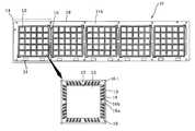
- FIGS. 1A-1Care plan views and bottom views of a circuit board according to the present invention.
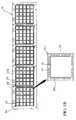
- FIG. 2Ais an enlarged plan view of a portion where the edges of the respective sub slots meet together in the circuit board according to the present invention
- FIG. 2Bis a cross-sectional view of the portion shown in FIG. 2A.
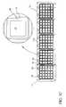
- FIG. 3is an enlarged plan view of portion A of the circuit board segment of FIG. 2A before a sub slot is formed therethrough.
- FIGS. 1A-1Care plan views and bottom views of a circuit board 10 according to the present invention.
- FIG. 2Ais an enlarged plan view of a portion where the edges of each sub slot 13 meet together in the circuit board 10 of the present invention, and
- FIG. 2Bis a cross-sectional view of the portion.
- the circuit board 10 of the present inventioncomprises a resin layer (in the form of film or tape) 17 , circuit patterns 18 , and an insulative cover coat 19 .
- the resin layer 17has a shape of rectangular sheet with opposing first and second sides 11 a and 11 b.
- Circuit board 10includes a plurality of 10 rectangular package units 10 - 1 . Each package unit 10 - 1 will form the internal circuit board of a singulated semiconductor package. Package units 10 - 1 each have a through hole 12 . A semiconductor chip will be mounted in each through hole, and suspended therein by a cover member, such as a removable tape, until an encapsulant material is applied to the chip and the respective package unit 10 - 1 . When the encapsulant material hardens, the encapsulant material will support the respective chip in through hole 12 .
- Package units 10 - 1 and through holes 12are arranged in rows and columns.
- Four sub slots 13surround each package unit 10 - 1 , one at each of the four sides of package units 10 - 1 .
- Adjacent package units 10 - 1are separated by and share a common sub slot 13 .
- Package units 10 - 1are grouped into rectangular sub strips 14 , each including rows and columns of package units 10 - 1 .
- a plurality of the sub strips 14are connected in a row and share a main slot 15 of a predetermined length as a common boundary, to form one main strip 16 .
- circuit board 10includes five sub strips 14 , each of which includes twenty five package units 10 - 1 .
- a main slot 15separates and is shared between adjacent sub strips 14 .
- both the sub slot 13 and the main slot 15are formed through resin layer 17 .
- the circuit patterns 18 of each package unit 10 - 1 of circuit board 10are formed from a known copper film and are provided on resin layer 17 between the respective through hole 12 and the surrounding sub slots 13 .
- Other metalse.g., copper alloys and aluminum may be used.
- the cover coat 19is formed from a known polymer resin and is applied to the surfaces of the circuit patterns 18 and the resin layer 17 in order to protect the circuit patterns 18 from the external environments.
- each of the circuit patterns 18 of each package unit 10 - 1 of circuit board 10includes a plurality of bond fingers 18 a, each of which will be connected later to the semiconductor chip, and a plurality of ball lands 18 b to which conductive balls will be fused later.
- the bond fingers 18 a and the ball lands 18 bare exposed through the cover coat 19 , as illustrated in the figures, to enable the metal-to-metal connections.
- Plating metalssuch as gold, silver, palladium, and nickel may be used to facilitate soldering.
- the circuit patterns 18may have both the bond fingers 18 a and the ball lands 18 b on second side 11 b of the resin layer 17 , as shown in FIG. 1A, or alternatively may have the ball lands 18 b on first side 11 a of the resin layer 17 and the bond fingers 18 a on the second side 11 b, as shown in FIG. 1 .
- the bond fingers 18 aare connected to the ball lands 18 b by conductive metal vias (not shown) that extend vertically through resin layer 17 .
- the ball lands 18 bare arranged in two rows in the figures, they can also be arranged in three to five rows. There is no particular limitation imposed on the number of rows of the arranged ball lands 18 b.
- a rectangular conductive ground ring 25may be formed on the first side 11 a of the resin layer 17 at the periphery of the individual through hole 12 of each package unit 10 - 1 of circuit board 10 , as is shown in FIG. 1 C.
- the ground ring 25is electrically connected to a circuit line of circuit pattern 18 of the package unit 10 - 1 .
- the ground ring 25is formed on first side 11 a opposite the side (i.e., opposite second side 11 b ) where the circuit patterns 18 , including the bond fingers 18 a and the ball lands 18 b , are formed.
- the ground ring 25is connected to the one or more circuit lines of the circuit patterns 18 through metal via holes (not shown) through resin layer 17 .
- ground ring 25provides grounding connection to the semiconductor chip and also enhances the rigidity of the entire circuit board 10 .
- the ground ring 25may be coated with the cover coat 19 or adhered to the surface of the resin layer 17 with an adhesive instead of coating, either of which method is a matter of personal choice of those skilled in the art.
- Ground ring 25ultimately may be electrically connected to the exposed backside of the semiconductor chip using, for example, a conductive ink.
- Conductive ground planes 24each having a predetermined area are formed on the surface of the resin layer 17 at the edge of the circuit board strip 10 .
- the ground plane 24is exposed through the cover coat 19 .
- the ground planes 24are each electrically connected to all or some of the circuit patterns, and also are electrically connected to the ground ring 25 (if present).
- the ground plane 24may be formed on both sides of the resin layer 17 so that the ground plane 24 or the ground ring 25 of the circuit board will come in contact with metal equipment during the process of fabrication, thereby facilitating discharge of any static electricity occurring in the circuit board.
- ground ring 25 and the ground plane 24are preferably formed from a copper film, there is no particular limitation imposed on the materials of the ground ring 25 and the ground plane 24 , as long as they have conductivity.
- a plurality of notches having a predetermined depthmay be formed in the resin layer 17 at one or both ends of the sub slots 13 of circuit board 10 .
- the notchesmay have a direction that is perpendicular to the lengthwise direction of the sub slot 13 .
- An exemplary notch 21 having a triangular shapeis shown in FIG. 2 B.
- Notch 21 of FIG. 2Bis formed in first side 11 a of resin layer and extends vertically into resin layer 17 .
- notch 21may be formed at second side 11 b of the resin layer 17 , or at both first side 11 a and second side 11 b of resin layer 17 . Formation of the notches 21 facilitates cutting of the circuit board 10 during a subsequent singulation process that separates out individual semiconductor package units.
- recognition marks 22there are formed recognition marks 22 between the sub slots 13 as a base point for wire bonding during a connection process.
- the recognition marks 22preferably have a cruciform shape.
- the recognition marks 22are formed at four corners of the through hole 12 so that the base point for wire bonding becomes easy to detect and distinguishable.
- the material of the recognition marks 22is preferably the same as that of the circuit patterns 18 .
- FIG. 3is a plan view of portion A of the portion of circuit board 10 that is shown in FIG. 2A before the sub slot 13 is formed as a boundary region of any one package unit 10 - 1 .
- a metal bus pattern 23 that is electrically connected to the circuit patterns 18 of each package unit 10 - 1 of circuit board 10is formed on the first side 11 a or the second side 11 b of the resin layer 17 .
- Bus pattern 23is laterally between the circuit patterns 18 of adjacent package units 10 - 1 , which are a predetermined distance from each other in the sub strip 14 .
- a defined portion of the bus pattern 23 and the resin layer 17 around the bus pattern 23are exposed to the outside through the cover coat 19 .
- bus pattern 23A large part of the portions exposed through the cover coat 19 , including the predefined portion of bus pattern 23 , will be punched out later to form the predefined sub slots 13 , which are shown in FIGS. 1A, 1 B and 2 A.
- the removal of bus pattern 23electrically isolates the circuit patterns of each of the the package units 10 - 1 , which previously were electrically connected by bus pattern 23 .
- an edge or coating line 19 a of the cover coat 19 where cover coat 19 crosses the circuit lines that connect each circuit patterns 18 to the bus pattern 23has the shape of an irregular profile.
- coating line 19 amay include protruding square portions 19 b, resembling a square wave, over the circuit lines, which reinforce the circuit lines during the punching of sub slot 13 .
- the resin layer 17is exposed through the cover coat 19 at the regions where the notches 21 and recognition marks 22 are formed.
- rows and columns of package units each having a through hole in which a semiconductor chip is to be locatedconstitute one sub strip, and a plurality of the sub strips are connected in a row to constitute one main strip.
- a plurality of notches formed in the resin layer between the sub slots that are along the periphery of the through holes of each package unitfacilitate singulation of the circuit board during a singulation process of the semiconductor packages after an encapsulation process.
- recognition marks formed in the resin layer between the sub slotsallow connection equipment, for example, wire bonding equipment, to accurately recognize the positions of the semiconductor chips and the circuit board, thereby providing an accurate wire bonding (electrical connection) between the semiconductor chips and the circuit board.
- a process of forming (punching out) the sub slotcan be easily performed because the cover coat is not applied to a sub slot forming region before the sub slot is formed in the circuit board.
- Embodiments of semiconductor packages and methods of making them that may employ the circuit board of the present inventionare disclosed in U.S. patent application Ser. No. 09/566,069, entitled “CIRCUIT BOARD FOR SEMICONDUCTOR PACKAGE,” which was filed on May 5, 2000; U.S. patent application Ser. No. 09/574,541, entitled “SEMICONDUCTOR PACKAGE AND METHOD FOR FABRICATING THE SAME,” which was filed on May 19, 2000 and issued as U.S. Pat. No. 6,395,598; and, U.S. patent application Ser. No. 09/574,006, entitled “SEMICONDUCTOR PACKAGE AND METHOD FOR MANUFACTURING THE SAME,” which also was filed on May 19, 2000. All three of these applications are incorporated herein by reference in their respective entireties.
Landscapes
- Engineering & Computer Science (AREA)
- Microelectronics & Electronic Packaging (AREA)
- Computer Hardware Design (AREA)
- Power Engineering (AREA)
- Physics & Mathematics (AREA)
- General Physics & Mathematics (AREA)
- Condensed Matter Physics & Semiconductors (AREA)
- Manufacturing & Machinery (AREA)
- Ceramic Engineering (AREA)
- Geometry (AREA)
- Structure Of Printed Boards (AREA)
- Wire Bonding (AREA)
- Structures Or Materials For Encapsulating Or Coating Semiconductor Devices Or Solid State Devices (AREA)
Abstract
Description
Claims (18)
Applications Claiming Priority (10)
| Application Number | Priority Date | Filing Date | Title |
|---|---|---|---|
| KR99-9992 | 1999-06-07 | ||
| KR2019990009992UKR20010000254U (en) | 1999-06-07 | 1999-06-07 | Substrate for semiconductor device |
| KR99-37925 | 1999-09-07 | ||
| KR10-1999-0037928AKR100369394B1 (en) | 1999-09-07 | 1999-09-07 | substrate for semiconductor package and manufacturing method of semiconductor package using it |
| KR99-37928 | 1999-09-07 | ||
| KR1019990037925AKR100365054B1 (en) | 1999-09-07 | 1999-09-07 | substrate for semiconductor package and manufacturing method of semiconductor package using it |
| KR99-48010 | 1999-11-01 | ||
| KR1019990048010AKR100355748B1 (en) | 1999-11-01 | 1999-11-01 | Substrate for manufacturing semiconductor package |
| KR99-65126 | 1999-12-29 | ||
| KR1019990065126AKR20010065254A (en) | 1999-12-29 | 1999-12-29 | Substrate for manufacturing semiconductor package |
Publications (1)
| Publication Number | Publication Date |
|---|---|
| US6512288B1true US6512288B1 (en) | 2003-01-28 |
Family
ID=27532301
Family Applications (1)
| Application Number | Title | Priority Date | Filing Date |
|---|---|---|---|
| US09/589,713Expired - LifetimeUS6512288B1 (en) | 1999-06-07 | 2000-06-07 | Circuit board semiconductor package |
Country Status (2)
| Country | Link |
|---|---|
| US (1) | US6512288B1 (en) |
| JP (1) | JP3314304B2 (en) |
Cited By (8)
| Publication number | Priority date | Publication date | Assignee | Title |
|---|---|---|---|---|
| US20030137035A1 (en)* | 2002-01-24 | 2003-07-24 | Siliconware Precision Industries Co., Ltd. | Substrate and fabrication method of the same |
| US20030194835A1 (en)* | 2002-04-10 | 2003-10-16 | Kim Joon Il | Method for fabricating ceramic chip packages |
| US20050023583A1 (en)* | 2001-06-11 | 2005-02-03 | Bolken Todd O. | Multi media card formed by transfer molding |
| US20060261957A1 (en)* | 2003-08-26 | 2006-11-23 | Ralf God | Method for producing bridge modules |
| US20070128747A1 (en)* | 2005-12-02 | 2007-06-07 | Semiconductor Energy Laboratory Co. | Method for manufacturing semiconductor device |
| US20070241438A1 (en)* | 2006-04-12 | 2007-10-18 | Samsung Electro-Mechanics Co., Ltd. | Strip format of package board and array of the same |
| US20100210142A1 (en)* | 2009-02-18 | 2010-08-19 | Cinch Connectors, Inc. | Electrical Connector |
| US11189610B2 (en)* | 2018-06-27 | 2021-11-30 | Advanced Semiconductor Engineering, Inc. | Substrate structure and manufacturing process |
Families Citing this family (3)
| Publication number | Priority date | Publication date | Assignee | Title |
|---|---|---|---|---|
| DE102004009567B4 (en)* | 2004-02-25 | 2007-01-04 | Infineon Technologies Ag | Wiring carrier for receiving chips |
| KR100826354B1 (en) | 2007-03-19 | 2008-05-02 | 삼성전기주식회사 | Package strips and their arrangement |
| KR101180635B1 (en)* | 2010-04-26 | 2012-09-18 | 주식회사 티엘아이 | Unit tape substrate reducing esd damage |
Citations (35)
| Publication number | Priority date | Publication date | Assignee | Title |
|---|---|---|---|---|
| US4530152A (en) | 1982-04-01 | 1985-07-23 | Compagnie Industrielle Des Telecommunications Cit-Alcatel | Method for encapsulating semiconductor components using temporary substrates |
| JPS629639A (en) | 1985-07-05 | 1987-01-17 | Nec Yamagata Ltd | Manufacture of semiconductor device |
| US4707724A (en) | 1984-06-04 | 1987-11-17 | Hitachi, Ltd. | Semiconductor device and method of manufacturing thereof |
| US4756080A (en) | 1986-01-27 | 1988-07-12 | American Microsystems, Inc. | Metal foil semiconductor interconnection method |
| US5157480A (en) | 1991-02-06 | 1992-10-20 | Motorola, Inc. | Semiconductor device having dual electrical contact sites |
| US5200362A (en) | 1989-09-06 | 1993-04-06 | Motorola, Inc. | Method of attaching conductive traces to an encapsulated semiconductor die using a removable transfer film |
| EP0682365A1 (en)* | 1994-05-10 | 1995-11-15 | Thomson-Csf | Three-dimensional interconnection of electronic component housings using printed circuits |
| US5474958A (en) | 1993-05-04 | 1995-12-12 | Motorola, Inc. | Method for making semiconductor device having no die supporting surface |
| US5474957A (en) | 1994-05-09 | 1995-12-12 | Nec Corporation | Process of mounting tape automated bonded semiconductor chip on printed circuit board through bumps |
| US5491612A (en)* | 1995-02-21 | 1996-02-13 | Fairchild Space And Defense Corporation | Three-dimensional modular assembly of integrated circuits |
| US5604376A (en) | 1994-06-30 | 1997-02-18 | Digital Equipment Corporation | Paddleless molded plastic semiconductor chip package |
| US5620928A (en) | 1995-05-11 | 1997-04-15 | National Semiconductor Corporation | Ultra thin ball grid array using a flex tape or printed wiring board substrate and method |
| US5646828A (en) | 1995-02-24 | 1997-07-08 | Lucent Technologies Inc. | Thin packaging of multi-chip modules with enhanced thermal/power management |
| US5652185A (en) | 1995-04-07 | 1997-07-29 | National Semiconductor Corporation | Maximized substrate design for grid array based assemblies |
| US5668405A (en) | 1994-09-14 | 1997-09-16 | Nec Corporation | Semiconductor device with a film carrier tape |
| US5696666A (en) | 1995-10-11 | 1997-12-09 | Motorola, Inc. | Low profile exposed die chip carrier package |
| US5776798A (en) | 1996-09-04 | 1998-07-07 | Motorola, Inc. | Semiconductor package and method thereof |
| US5819398A (en)* | 1995-07-31 | 1998-10-13 | Sgs-Thomson Microelectronics, Ltd. | Method of manufacturing a ball grid array package |
| US5835355A (en) | 1997-09-22 | 1998-11-10 | Lsi Logic Corporation | Tape ball grid array package with perforated metal stiffener |
| US5854741A (en)* | 1995-11-17 | 1998-12-29 | Amkor Electronics, Inc. | Unit printed circuit board carrier frame for ball grid array semiconductor packages and method for fabricating ball grid array semiconductor packages using the same |
| US5859471A (en) | 1992-11-17 | 1999-01-12 | Shinko Electric Industries Co., Ltd. | Semiconductor device having tab tape lead frame with reinforced outer leads |
| US5866949A (en)* | 1996-12-02 | 1999-02-02 | Minnesota Mining And Manufacturing Company | Chip scale ball grid array for integrated circuit packaging |
| US5894108A (en) | 1997-02-11 | 1999-04-13 | National Semiconductor Corporation | Plastic package with exposed die |
| US5903052A (en) | 1998-05-12 | 1999-05-11 | Industrial Technology Research Institute | Structure for semiconductor package for improving the efficiency of spreading heat |
| JPH11354682A (en)* | 1998-05-27 | 1999-12-24 | Anam Semiconductor Inc | Printed circuit board |
| US6013948A (en) | 1995-11-27 | 2000-01-11 | Micron Technology, Inc. | Stackable chip scale semiconductor package with mating contacts on opposed surfaces |
| US6034423A (en) | 1998-04-02 | 2000-03-07 | National Semiconductor Corporation | Lead frame design for increased chip pinout |
| US6034427A (en) | 1998-01-28 | 2000-03-07 | Prolinx Labs Corporation | Ball grid array structure and method for packaging an integrated circuit chip |
| US6100804A (en) | 1998-10-29 | 2000-08-08 | Intecmec Ip Corp. | Radio frequency identification system |
| US6099677A (en) | 1998-02-13 | 2000-08-08 | Merrimac Industries, Inc. | Method of making microwave, multifunction modules using fluoropolymer composite substrates |
| US6107689A (en) | 1996-07-30 | 2000-08-22 | Kabushiki Kaisha Toshiba | Semiconductor device |
| US6127833A (en) | 1999-01-04 | 2000-10-03 | Taiwan Semiconductor Manufacturing Co. | Test carrier for attaching a semiconductor device |
| US6172419B1 (en) | 1998-02-24 | 2001-01-09 | Micron Technology, Inc. | Low profile ball grid array package |
| US6257857B1 (en)* | 2000-01-31 | 2001-07-10 | Advanced Semiconductor Engineering, Inc. | Molding apparatus for flexible substrate based package |
| US6262490B1 (en)* | 1999-11-05 | 2001-07-17 | Advanced Semiconductor Engineering, Inc. | Substrate strip for use in packaging semiconductor chips |
Family Cites Families (2)
| Publication number | Priority date | Publication date | Assignee | Title |
|---|---|---|---|---|
| WO1997048133A1 (en) | 1996-06-14 | 1997-12-18 | Siemens Aktiengesellschaft | Carrier element for semiconductor chips |
| JP2001298121A (en) | 2000-04-17 | 2001-10-26 | Suzuki Co Ltd | Film for electronic component, its manufacturing method and die to be used therefor |
- 2000
- 2000-04-24JPJP2000123164Apatent/JP3314304B2/ennot_activeExpired - Fee Related
- 2000-06-07USUS09/589,713patent/US6512288B1/ennot_activeExpired - Lifetime
Patent Citations (36)
| Publication number | Priority date | Publication date | Assignee | Title |
|---|---|---|---|---|
| US4530152A (en) | 1982-04-01 | 1985-07-23 | Compagnie Industrielle Des Telecommunications Cit-Alcatel | Method for encapsulating semiconductor components using temporary substrates |
| US4707724A (en) | 1984-06-04 | 1987-11-17 | Hitachi, Ltd. | Semiconductor device and method of manufacturing thereof |
| JPS629639A (en) | 1985-07-05 | 1987-01-17 | Nec Yamagata Ltd | Manufacture of semiconductor device |
| US4756080A (en) | 1986-01-27 | 1988-07-12 | American Microsystems, Inc. | Metal foil semiconductor interconnection method |
| US5200362A (en) | 1989-09-06 | 1993-04-06 | Motorola, Inc. | Method of attaching conductive traces to an encapsulated semiconductor die using a removable transfer film |
| US5273938A (en) | 1989-09-06 | 1993-12-28 | Motorola, Inc. | Method for attaching conductive traces to plural, stacked, encapsulated semiconductor die using a removable transfer film |
| US5157480A (en) | 1991-02-06 | 1992-10-20 | Motorola, Inc. | Semiconductor device having dual electrical contact sites |
| US5859471A (en) | 1992-11-17 | 1999-01-12 | Shinko Electric Industries Co., Ltd. | Semiconductor device having tab tape lead frame with reinforced outer leads |
| US5474958A (en) | 1993-05-04 | 1995-12-12 | Motorola, Inc. | Method for making semiconductor device having no die supporting surface |
| US5474957A (en) | 1994-05-09 | 1995-12-12 | Nec Corporation | Process of mounting tape automated bonded semiconductor chip on printed circuit board through bumps |
| EP0682365A1 (en)* | 1994-05-10 | 1995-11-15 | Thomson-Csf | Three-dimensional interconnection of electronic component housings using printed circuits |
| US5604376A (en) | 1994-06-30 | 1997-02-18 | Digital Equipment Corporation | Paddleless molded plastic semiconductor chip package |
| US5668405A (en) | 1994-09-14 | 1997-09-16 | Nec Corporation | Semiconductor device with a film carrier tape |
| US5491612A (en)* | 1995-02-21 | 1996-02-13 | Fairchild Space And Defense Corporation | Three-dimensional modular assembly of integrated circuits |
| US5646828A (en) | 1995-02-24 | 1997-07-08 | Lucent Technologies Inc. | Thin packaging of multi-chip modules with enhanced thermal/power management |
| US5652185A (en) | 1995-04-07 | 1997-07-29 | National Semiconductor Corporation | Maximized substrate design for grid array based assemblies |
| US5620928A (en) | 1995-05-11 | 1997-04-15 | National Semiconductor Corporation | Ultra thin ball grid array using a flex tape or printed wiring board substrate and method |
| US5819398A (en)* | 1995-07-31 | 1998-10-13 | Sgs-Thomson Microelectronics, Ltd. | Method of manufacturing a ball grid array package |
| US5696666A (en) | 1995-10-11 | 1997-12-09 | Motorola, Inc. | Low profile exposed die chip carrier package |
| US5854741A (en)* | 1995-11-17 | 1998-12-29 | Amkor Electronics, Inc. | Unit printed circuit board carrier frame for ball grid array semiconductor packages and method for fabricating ball grid array semiconductor packages using the same |
| US6013948A (en) | 1995-11-27 | 2000-01-11 | Micron Technology, Inc. | Stackable chip scale semiconductor package with mating contacts on opposed surfaces |
| US6107689A (en) | 1996-07-30 | 2000-08-22 | Kabushiki Kaisha Toshiba | Semiconductor device |
| US5776798A (en) | 1996-09-04 | 1998-07-07 | Motorola, Inc. | Semiconductor package and method thereof |
| US5866949A (en)* | 1996-12-02 | 1999-02-02 | Minnesota Mining And Manufacturing Company | Chip scale ball grid array for integrated circuit packaging |
| US5894108A (en) | 1997-02-11 | 1999-04-13 | National Semiconductor Corporation | Plastic package with exposed die |
| US5835355A (en) | 1997-09-22 | 1998-11-10 | Lsi Logic Corporation | Tape ball grid array package with perforated metal stiffener |
| US6034427A (en) | 1998-01-28 | 2000-03-07 | Prolinx Labs Corporation | Ball grid array structure and method for packaging an integrated circuit chip |
| US6099677A (en) | 1998-02-13 | 2000-08-08 | Merrimac Industries, Inc. | Method of making microwave, multifunction modules using fluoropolymer composite substrates |
| US6172419B1 (en) | 1998-02-24 | 2001-01-09 | Micron Technology, Inc. | Low profile ball grid array package |
| US6034423A (en) | 1998-04-02 | 2000-03-07 | National Semiconductor Corporation | Lead frame design for increased chip pinout |
| US5903052A (en) | 1998-05-12 | 1999-05-11 | Industrial Technology Research Institute | Structure for semiconductor package for improving the efficiency of spreading heat |
| JPH11354682A (en)* | 1998-05-27 | 1999-12-24 | Anam Semiconductor Inc | Printed circuit board |
| US6100804A (en) | 1998-10-29 | 2000-08-08 | Intecmec Ip Corp. | Radio frequency identification system |
| US6127833A (en) | 1999-01-04 | 2000-10-03 | Taiwan Semiconductor Manufacturing Co. | Test carrier for attaching a semiconductor device |
| US6262490B1 (en)* | 1999-11-05 | 2001-07-17 | Advanced Semiconductor Engineering, Inc. | Substrate strip for use in packaging semiconductor chips |
| US6257857B1 (en)* | 2000-01-31 | 2001-07-10 | Advanced Semiconductor Engineering, Inc. | Molding apparatus for flexible substrate based package |
Cited By (16)
| Publication number | Priority date | Publication date | Assignee | Title |
|---|---|---|---|---|
| US20050023583A1 (en)* | 2001-06-11 | 2005-02-03 | Bolken Todd O. | Multi media card formed by transfer molding |
| US6943439B2 (en)* | 2002-01-24 | 2005-09-13 | Siliconware Precision Industries Co., Ltd. | Substrate and fabrication method of the same |
| US20030137035A1 (en)* | 2002-01-24 | 2003-07-24 | Siliconware Precision Industries Co., Ltd. | Substrate and fabrication method of the same |
| US20030194835A1 (en)* | 2002-04-10 | 2003-10-16 | Kim Joon Il | Method for fabricating ceramic chip packages |
| US6818473B2 (en)* | 2002-04-10 | 2004-11-16 | Samsung Electro-Mechanics Co., Ltd. | Method for fabricating ceramic chip packages |
| US20060261957A1 (en)* | 2003-08-26 | 2006-11-23 | Ralf God | Method for producing bridge modules |
| US7875530B2 (en)* | 2005-12-02 | 2011-01-25 | Semiconductor Energy Laboratory Co., Ltd. | Method for manufacturing semiconductor device |
| US20070128747A1 (en)* | 2005-12-02 | 2007-06-07 | Semiconductor Energy Laboratory Co. | Method for manufacturing semiconductor device |
| US20070241438A1 (en)* | 2006-04-12 | 2007-10-18 | Samsung Electro-Mechanics Co., Ltd. | Strip format of package board and array of the same |
| US20100210142A1 (en)* | 2009-02-18 | 2010-08-19 | Cinch Connectors, Inc. | Electrical Connector |
| US20110195592A1 (en)* | 2009-02-18 | 2011-08-11 | Cinch Connectors, Inc. | Electrical Connector |
| US20110195593A1 (en)* | 2009-02-18 | 2011-08-11 | Cinch Connectors, Inc. | Electrical Connector |
| US8011950B2 (en) | 2009-02-18 | 2011-09-06 | Cinch Connectors, Inc. | Electrical connector |
| US8298009B2 (en) | 2009-02-18 | 2012-10-30 | Cinch Connectors, Inc. | Cable assembly with printed circuit board having a ground layer |
| US8337243B2 (en) | 2009-02-18 | 2012-12-25 | Cinch Connectors, Inc. | Cable assembly with a material at an edge of a substrate |
| US11189610B2 (en)* | 2018-06-27 | 2021-11-30 | Advanced Semiconductor Engineering, Inc. | Substrate structure and manufacturing process |
Also Published As
| Publication number | Publication date |
|---|---|
| JP2001007253A (en) | 2001-01-12 |
| JP3314304B2 (en) | 2002-08-12 |
Similar Documents
| Publication | Publication Date | Title |
|---|---|---|
| US6664615B1 (en) | Method and apparatus for lead-frame based grid array IC packaging | |
| US8659151B2 (en) | Semiconductor device and manufacturing method thereof | |
| US6713322B2 (en) | Lead frame for semiconductor package | |
| US6281568B1 (en) | Plastic integrated circuit device package and leadframe having partially undercut leads and die pad | |
| US6525406B1 (en) | Semiconductor device having increased moisture path and increased solder joint strength | |
| US7745910B1 (en) | Semiconductor device having RF shielding and method therefor | |
| US6972214B2 (en) | Method for fabricating a semiconductor package with multi layered leadframe | |
| KR100319609B1 (en) | A wire arrayed chip size package and the fabrication method thereof | |
| US6677219B2 (en) | Method of forming a ball grid array package | |
| US20050051882A1 (en) | Stacked chip package having upper chip provided with trenches and method of manufacturing the same | |
| US5849608A (en) | Semiconductor chip package | |
| US8115288B2 (en) | Lead frame for semiconductor device | |
| US6479887B1 (en) | Circuit pattern tape for wafer-scale production of chip size semiconductor packages | |
| JP2002514014A (en) | Chip laminate and manufacturing method thereof | |
| US10096555B2 (en) | Shielded QFN package and method of making | |
| US6512288B1 (en) | Circuit board semiconductor package | |
| US12255076B2 (en) | Method for manufacturing leadless semiconductor package with wettable flanks | |
| US20050046035A1 (en) | Semiconductor device | |
| EP3319122B1 (en) | Semiconductor device with wettable corner leads | |
| JP2000150702A (en) | Manufacture of semiconductor device | |
| US5406119A (en) | Lead frame | |
| US6278618B1 (en) | Substrate strips for use in integrated circuit packaging | |
| JPH04233244A (en) | Integrated-circuit assembly | |
| US20060097408A1 (en) | Semiconductor package device and method for fabricating the same | |
| US11309237B2 (en) | Semiconductor package with wettable slot structures |
Legal Events
| Date | Code | Title | Description |
|---|---|---|---|
| AS | Assignment | Owner name:AMKOR TECHNOLOGY, INC., ARIZONA Free format text:ASSIGNMENT OF ASSIGNORS INTEREST;ASSIGNORS:SHIN, WONSUN;LEE, SEONGOO;JANG, TAEHOAN;AND OTHERS;REEL/FRAME:010876/0382 Effective date:20000605 | |
| AS | Assignment | Owner name:AMKOR TECHNOLOGY, INC., ARIZONA Free format text:ASSIGNMENT OF ASSIGNORS INTEREST;ASSIGNOR:DICAPRIO, VINCENT;REEL/FRAME:011156/0022 Effective date:20000806 Owner name:AMKOR TECHNOLOGY KOREA, INC., KOREA, REPUBLIC OF Free format text:ASSIGNMENT OF ASSIGNORS INTEREST;ASSIGNOR:DICAPRIO, VINCENT;REEL/FRAME:011156/0022 Effective date:20000806 | |
| AS | Assignment | Owner name:AMKOR TECHNOLOGY, INC., ARIZONA Free format text:ASSIGNMENT OF ASSIGNORS INTEREST;ASSIGNOR:AMKOR TECHNOLOGY KOREA, INC.;REEL/FRAME:013323/0853 Effective date:20020913 | |
| STCF | Information on status: patent grant | Free format text:PATENTED CASE | |
| AS | Assignment | Owner name:CITICORP NORTH AMERICA, INC. AS ADMINISTRATIVE AGE Free format text:SECURITY AGREEMENT;ASSIGNORS:AMKOR TECHNOLOGY, INC.;GUARDIAN ASSETS, INC.;REEL/FRAME:014885/0691 Effective date:20040629 | |
| AS | Assignment | Owner name:CITICORP NORTH AMERICA, INC. AS "AGENT", NEW YORK Free format text:SECURITY AGREEMENT;ASSIGNORS:AMKOR TECHNOLOGY, INC.;GUARDIAN ASSETS, INC.;REEL/FRAME:015942/0521 Effective date:20041027 | |
| AS | Assignment | Owner name:AMKOR TECHNOLOGY, INC., ARIZONA Free format text:TERMINATION & RELEASE OF PATENT SECURITY AGREEMENT;ASSIGNOR:CITICORP NORTH AMERICA, INC.;REEL/FRAME:017388/0868 Effective date:20051128 Owner name:BANK OF AMERICA, N.A., TEXAS Free format text:SECURITY AGREEMENT;ASSIGNOR:AMKOR TECHNOLOGY, INC.;REEL/FRAME:017379/0630 Effective date:20051123 | |
| FPAY | Fee payment | Year of fee payment:4 | |
| FPAY | Fee payment | Year of fee payment:8 | |
| FPAY | Fee payment | Year of fee payment:12 | |
| AS | Assignment | Owner name:BANK OF AMERICA, N.A., AS AGENT, CALIFORNIA Free format text:SECURITY INTEREST;ASSIGNOR:AMKOR TECHNOLOGY, INC.;REEL/FRAME:046683/0139 Effective date:20180713 | |
| AS | Assignment | Owner name:AMKOR TECHNOLOGY SINGAPORE HOLDING PTE.LTD., SINGAPORE Free format text:ASSIGNMENT OF ASSIGNORS INTEREST;ASSIGNOR:AMKOR TECHNOLOGY, INC.;REEL/FRAME:054067/0135 Effective date:20191119 |