US6511867B2 - Utilizing atomic layer deposition for programmable device - Google Patents
Utilizing atomic layer deposition for programmable deviceDownload PDFInfo
- Publication number
- US6511867B2 US6511867B2US09/896,529US89652901AUS6511867B2US 6511867 B2US6511867 B2US 6511867B2US 89652901 AUS89652901 AUS 89652901AUS 6511867 B2US6511867 B2US 6511867B2
- Authority
- US
- United States
- Prior art keywords
- memory
- electrode
- forming
- dielectric
- depicts
- Prior art date
- Legal status (The legal status is an assumption and is not a legal conclusion. Google has not performed a legal analysis and makes no representation as to the accuracy of the status listed.)
- Expired - Lifetime
Links
- 238000000231atomic layer depositionMethods0.000titleclaimsdescription16
- 239000000463materialSubstances0.000claimsdescription63
- 238000000034methodMethods0.000claimsdescription21
- 239000000758substrateSubstances0.000claimsdescription20
- 230000004888barrier functionEffects0.000claimsdescription15
- 239000004020conductorSubstances0.000claimsdescription14
- 238000000151depositionMethods0.000claimsdescription8
- 150000004770chalcogenidesChemical class0.000claimsdescription6
- 229910052581Si3N4Inorganic materials0.000claimsdescription5
- NRTOMJZYCJJWKI-UHFFFAOYSA-NTitanium nitrideChemical compound[Ti]#NNRTOMJZYCJJWKI-UHFFFAOYSA-N0.000claimsdescription5
- WFKWXMTUELFFGS-UHFFFAOYSA-NtungstenChemical compound[W]WFKWXMTUELFFGS-UHFFFAOYSA-N0.000claimsdescription3
- 229910052721tungstenInorganic materials0.000claimsdescription3
- 239000010937tungstenSubstances0.000claimsdescription3
- UGACIEPFGXRWCH-UHFFFAOYSA-N[Si].[Ti]Chemical compound[Si].[Ti]UGACIEPFGXRWCH-UHFFFAOYSA-N0.000claimsdescription2
- IVHJCRXBQPGLOV-UHFFFAOYSA-NazanylidynetungstenChemical compound[W]#NIVHJCRXBQPGLOV-UHFFFAOYSA-N0.000claimsdescription2
- MZLGASXMSKOWSE-UHFFFAOYSA-Ntantalum nitrideChemical compound[Ta]#NMZLGASXMSKOWSE-UHFFFAOYSA-N0.000claimsdescription2
- 229910021341titanium silicideInorganic materials0.000claims1
- 239000003989dielectric materialSubstances0.000description18
- VYPSYNLAJGMNEJ-UHFFFAOYSA-NSilicium dioxideChemical compoundO=[Si]=OVYPSYNLAJGMNEJ-UHFFFAOYSA-N0.000description16
- 239000007772electrode materialSubstances0.000description12
- XUIMIQQOPSSXEZ-UHFFFAOYSA-NSiliconChemical compound[Si]XUIMIQQOPSSXEZ-UHFFFAOYSA-N0.000description9
- 239000002019doping agentSubstances0.000description9
- 238000002955isolationMethods0.000description9
- 229910052710siliconInorganic materials0.000description9
- 239000010703siliconSubstances0.000description9
- 230000015572biosynthetic processEffects0.000description8
- 239000010408filmSubstances0.000description8
- 239000000377silicon dioxideSubstances0.000description8
- 230000008859changeEffects0.000description7
- 239000007789gasSubstances0.000description7
- 230000000873masking effectEffects0.000description7
- 239000010410layerSubstances0.000description6
- 238000000059patterningMethods0.000description6
- 239000004065semiconductorSubstances0.000description6
- 239000012782phase change materialSubstances0.000description5
- 229910004298SiO 2Inorganic materials0.000description4
- -1i.e.Substances0.000description4
- 239000010936titaniumSubstances0.000description4
- 238000005229chemical vapour depositionMethods0.000description3
- 230000005669field effectEffects0.000description3
- 238000004519manufacturing processMethods0.000description3
- 239000002243precursorSubstances0.000description3
- 230000008569processEffects0.000description3
- 230000002829reductive effectEffects0.000description3
- HQVNEWCFYHHQES-UHFFFAOYSA-Nsilicon nitrideChemical compoundN12[Si]34N5[Si]62N3[Si]51N64HQVNEWCFYHHQES-UHFFFAOYSA-N0.000description3
- 239000007787solidSubstances0.000description3
- 229910000838Al alloyInorganic materials0.000description2
- RTAQQCXQSZGOHL-UHFFFAOYSA-NTitaniumChemical compound[Ti]RTAQQCXQSZGOHL-UHFFFAOYSA-N0.000description2
- 229910045601alloyInorganic materials0.000description2
- 239000000956alloySubstances0.000description2
- 229910052782aluminiumInorganic materials0.000description2
- XAGFODPZIPBFFR-UHFFFAOYSA-NaluminiumChemical compound[Al]XAGFODPZIPBFFR-UHFFFAOYSA-N0.000description2
- 238000000277atomic layer chemical vapour depositionMethods0.000description2
- 238000010276constructionMethods0.000description2
- 230000008021depositionEffects0.000description2
- 238000010586diagramMethods0.000description2
- 238000005530etchingMethods0.000description2
- 230000004048modificationEffects0.000description2
- 238000012986modificationMethods0.000description2
- 235000012239silicon dioxideNutrition0.000description2
- 239000002356single layerSubstances0.000description2
- 229910052719titaniumInorganic materials0.000description2
- 229910000763AgInSbTeInorganic materials0.000description1
- ZOXJGFHDIHLPTG-UHFFFAOYSA-NBoronChemical compound[B]ZOXJGFHDIHLPTG-UHFFFAOYSA-N0.000description1
- 206010010144Completed suicideDiseases0.000description1
- 229910005542GaSbInorganic materials0.000description1
- 229910005537GaSeTeInorganic materials0.000description1
- 229910005872GeSbInorganic materials0.000description1
- 229910005898GeSnInorganic materials0.000description1
- 229910005900GeTeInorganic materials0.000description1
- 229910017629Sb2Te3Inorganic materials0.000description1
- 229910018321SbTeInorganic materials0.000description1
- 229910018219SeTeInorganic materials0.000description1
- 229910006905SnSb2Te4Inorganic materials0.000description1
- 229910004284Te81Ge15Sb2S2Inorganic materials0.000description1
- 239000004964aerogelSubstances0.000description1
- 229910052785arsenicInorganic materials0.000description1
- RQNWIZPPADIBDY-UHFFFAOYSA-Narsenic atomChemical compound[As]RQNWIZPPADIBDY-UHFFFAOYSA-N0.000description1
- 229910052796boronInorganic materials0.000description1
- 229910010293ceramic materialInorganic materials0.000description1
- 238000006243chemical reactionMethods0.000description1
- 239000010941cobaltSubstances0.000description1
- 229910017052cobaltInorganic materials0.000description1
- GUTLYIVDDKVIGB-UHFFFAOYSA-Ncobalt atomChemical compound[Co]GUTLYIVDDKVIGB-UHFFFAOYSA-N0.000description1
- 238000004590computer programMethods0.000description1
- 230000003247decreasing effectEffects0.000description1
- 238000009792diffusion processMethods0.000description1
- 230000007717exclusionEffects0.000description1
- 239000011521glassSubstances0.000description1
- BHEPBYXIRTUNPN-UHFFFAOYSA-Nhydridophosphorus(.) (triplet)Chemical compound[PH]BHEPBYXIRTUNPN-UHFFFAOYSA-N0.000description1
- 230000006872improvementEffects0.000description1
- WPYVAWXEWQSOGY-UHFFFAOYSA-Nindium antimonideChemical compound[Sb]#[In]WPYVAWXEWQSOGY-UHFFFAOYSA-N0.000description1
- 230000002452interceptive effectEffects0.000description1
- 230000005055memory storageEffects0.000description1
- 229910044991metal oxideInorganic materials0.000description1
- 150000004706metal oxidesChemical class0.000description1
- 238000004377microelectronicMethods0.000description1
- 238000002156mixingMethods0.000description1
- 239000011368organic materialSubstances0.000description1
- 230000000737periodic effectEffects0.000description1
- 230000002093peripheral effectEffects0.000description1
- 238000000206photolithographyMethods0.000description1
- 229910021420polycrystalline siliconInorganic materials0.000description1
- 229920000642polymerPolymers0.000description1
- 229920005591polysiliconPolymers0.000description1
- 239000000376reactantSubstances0.000description1
- 230000009467reductionEffects0.000description1
- 239000003870refractory metalSubstances0.000description1
- 238000009877renderingMethods0.000description1
- 230000008672reprogrammingEffects0.000description1
- 230000000717retained effectEffects0.000description1
- FESBVLZDDCQLFY-UHFFFAOYSA-NseteChemical compound[Te]=[Se]FESBVLZDDCQLFY-UHFFFAOYSA-N0.000description1
- 229910021332silicideInorganic materials0.000description1
- FVBUAEGBCNSCDD-UHFFFAOYSA-Nsilicide(4-)Chemical compound[Si-4]FVBUAEGBCNSCDD-UHFFFAOYSA-N0.000description1
- 238000001228spectrumMethods0.000description1
- 230000003068static effectEffects0.000description1
- 239000000126substanceSubstances0.000description1
- 238000006557surface reactionMethods0.000description1
- 239000010409thin filmSubstances0.000description1
Images


Classifications
- H—ELECTRICITY
- H01—ELECTRIC ELEMENTS
- H01L—SEMICONDUCTOR DEVICES NOT COVERED BY CLASS H10
- H01L21/00—Processes or apparatus adapted for the manufacture or treatment of semiconductor or solid state devices or of parts thereof
- H01L21/70—Manufacture or treatment of devices consisting of a plurality of solid state components formed in or on a common substrate or of parts thereof; Manufacture of integrated circuit devices or of parts thereof
- H01L21/71—Manufacture of specific parts of devices defined in group H01L21/70
- H01L21/768—Applying interconnections to be used for carrying current between separate components within a device comprising conductors and dielectrics
- H01L21/76838—Applying interconnections to be used for carrying current between separate components within a device comprising conductors and dielectrics characterised by the formation and the after-treatment of the conductors
- H01L21/76841—Barrier, adhesion or liner layers
- H01L21/7685—Barrier, adhesion or liner layers the layer covering a conductive structure
- H—ELECTRICITY
- H01—ELECTRIC ELEMENTS
- H01L—SEMICONDUCTOR DEVICES NOT COVERED BY CLASS H10
- H01L21/00—Processes or apparatus adapted for the manufacture or treatment of semiconductor or solid state devices or of parts thereof
- H01L21/02—Manufacture or treatment of semiconductor devices or of parts thereof
- H01L21/04—Manufacture or treatment of semiconductor devices or of parts thereof the devices having potential barriers, e.g. a PN junction, depletion layer or carrier concentration layer
- H01L21/18—Manufacture or treatment of semiconductor devices or of parts thereof the devices having potential barriers, e.g. a PN junction, depletion layer or carrier concentration layer the devices having semiconductor bodies comprising elements of Group IV of the Periodic Table or AIIIBV compounds with or without impurities, e.g. doping materials
- H01L21/28—Manufacture of electrodes on semiconductor bodies using processes or apparatus not provided for in groups H01L21/20 - H01L21/268
- H01L21/283—Deposition of conductive or insulating materials for electrodes conducting electric current
- H01L21/285—Deposition of conductive or insulating materials for electrodes conducting electric current from a gas or vapour, e.g. condensation
- H01L21/28506—Deposition of conductive or insulating materials for electrodes conducting electric current from a gas or vapour, e.g. condensation of conductive layers
- H01L21/28512—Deposition of conductive or insulating materials for electrodes conducting electric current from a gas or vapour, e.g. condensation of conductive layers on semiconductor bodies comprising elements of Group IV of the Periodic Table
- H01L21/28556—Deposition of conductive or insulating materials for electrodes conducting electric current from a gas or vapour, e.g. condensation of conductive layers on semiconductor bodies comprising elements of Group IV of the Periodic Table by chemical means, e.g. CVD, LPCVD, PECVD, laser CVD
- H01L21/28562—Selective deposition
- H—ELECTRICITY
- H01—ELECTRIC ELEMENTS
- H01L—SEMICONDUCTOR DEVICES NOT COVERED BY CLASS H10
- H01L21/00—Processes or apparatus adapted for the manufacture or treatment of semiconductor or solid state devices or of parts thereof
- H01L21/70—Manufacture or treatment of devices consisting of a plurality of solid state components formed in or on a common substrate or of parts thereof; Manufacture of integrated circuit devices or of parts thereof
- H01L21/71—Manufacture of specific parts of devices defined in group H01L21/70
- H01L21/768—Applying interconnections to be used for carrying current between separate components within a device comprising conductors and dielectrics
- H01L21/76838—Applying interconnections to be used for carrying current between separate components within a device comprising conductors and dielectrics characterised by the formation and the after-treatment of the conductors
- H01L21/76886—Modifying permanently or temporarily the pattern or the conductivity of conductive members, e.g. formation of alloys, reduction of contact resistances
- H01L21/76888—By rendering at least a portion of the conductor non conductive, e.g. oxidation
- H—ELECTRICITY
- H10—SEMICONDUCTOR DEVICES; ELECTRIC SOLID-STATE DEVICES NOT OTHERWISE PROVIDED FOR
- H10B—ELECTRONIC MEMORY DEVICES
- H10B63/00—Resistance change memory devices, e.g. resistive RAM [ReRAM] devices
- H10B63/10—Phase change RAM [PCRAM, PRAM] devices
Definitions
- Phase change memory devicesincluding phase change memory devices that can be programmed by modifying the state of a phase change material.
- RAMrandom access memory
- ROMread-only memory
- Typical memory applicationsinclude dynamic random access memory (DRAM), static random access memory (SRAM), erasable programmable read-only memory (EPROM), and electrically erasable programmable read-only memory (EEPROM).
- DRAMdynamic random access memory
- SRAMstatic random access memory
- EPROMerasable programmable read-only memory
- EEPROMelectrically erasable programmable read-only memory
- Solid state memory devicestypically employ micro-electronic circuit elements for each memory bit (e.g., one to four transistors per bit) in memory applications. Since one or more electronic circuit elements are required for each memory bit, these devices may consume considerable chip “real estate” to store a bit of information, which limits the density of a memory chip.
- the primary “non-volatile” memory element of these devicessuch as an EEPRROM, typically employ a floating gate field effect transistor device that has limited re-programmability and which holds a charge on the gate of field effect transistor to store each memory bit. These classes of memory devices are also relatively slow to program.
- Phase change memory devicesuse phase change materials, i.e., materials that can be electrically switched between a generally amorphous and a generally crystalline state, for electronic memory application.
- phase change materialsi.e., materials that can be electrically switched between a generally amorphous and a generally crystalline state
- One type of memory element originally developed by Energy Conversion Devices, Inc. of Troy, Mich.utilizes a phase change material that can be, in one application, electrically switched between a structural state of generally amorphous and generally crystalline local order or between different detectable states of local order across the entire spectrum between completely amorphous and completely crystalline states.
- Typical materials suitable for such applicationinclude those utilizing various chalcogenide elements.
- These electrical memory devicestypically do not use field effect transistor devices as the memory storage element, but comprise, in the electrical context, a monolithic body of thin film chalcogenide material.
- phase change memory materialsrepresent a significant improvement in non-volatile memory.
- One characteristic common to solid state and phase change memory devicesis significant power consumption particularly in setting or reprogramming memory elements. Power consumption is significant, particularly in portable devices that rely on power cells (e.g., batteries). It would be desirable to decrease the power consumption of a memory device.
- power cellse.g., batteries
- phase change memory materialAnother characteristic common to solid state and phase change memory devices is limited reprogrammable cycle life from/to an amorphous and crystalline state. Further, over time the phase change material can fail to reliably reprogram from/to an amorphous and a crystalline state. It would be desirable to increase the programmable cycle life of the phase change memory material.
- FIG. 1is a schematic diagram of an embodiment of an array of memory elements
- FIG. 2schematically illustrates a cross-sectional planar side view of a portion of a semiconductor substrate having dielectric trenches formed therein defining a z-direction thickness of a memory cell in accordance with one embodiment of forming a memory element on a substrate;
- FIG. 3depicts the structure of FIG. 2, through the same cross-sectional view, after the introduction of dopants to form an isolation device for a memory element;
- FIG. 4depicts the structure of FIG. 3 forming trenches
- FIG. 5depicts a schematic top view of the structure of FIG. 4;
- FIG. 6depicts a cross-section of the structure of FIG. 4 after forming contacts
- FIG. 7depicts the structure of FIG. 6, through the same cross-sectional view, after forming a masking material and a dielectric material;
- FIG. 8depicts the structure of FIG. 7, through the same cross-sectional view, after the formation of an opening through the dielectric exposing the contact;
- FIG. 9depicts the structure of FIG. 8, through the same cross-sectional view, showing the creation of electrode monolayers on the dielectric and on the contact, utilizing ALD;
- FIG. 10depicts the structure of FIG. 9, through the same cross-sectional view, after conformally forming the electrode on the dielectric and on the contact;
- FIG. 11depicts the structure of FIG. 10, through the same cross-sectional view, after forming a dielectric in the opening and removing a horizontal portion of the electrode;
- FIG. 12depicts the structure of FIG. 11, through the same cross-sectional view, after conformally forming a barrier on the electrode, utilizing ALD;
- FIG. 13depicts the structure of FIG. 12, through the same cross-sectional view, after forming and patterning a programmable material, a barrier and a conductor;
- FIG. 14depicts the structure of FIG. 13, through the same cross-sectional view, after forming a dielectric on the conductor, forming a via, and forming a signal line on the dielectric;
- FIG. 15depicts a method of forming a memory device having a structure similar to that described by FIG. 14;
- FIG. 16depicts one system embodiment including a memory having a structure similar to that described by FIG. 14 .
- a memory device utilizing programmable material to determine the state of memory elements of the deviceis described that reprograms to an amorphous and crystalline state.
- the described memory device and methodprovides improved device reliability, improved programmable cycle life and decreased power consumption relative to previous devices. Further, in an embodiment, the apparatus is manufacturable utilizing conventional process toolsets and facilities.
- atomic layer depositionprovides electrode device construction advantages, including reduction of required programming current for a reset, set and read operation in the memory device.
- ALDatomic layer deposition
- ALDatomic layer deposition
- CVDchemical vapor deposition
- electrode device construction advantagesare provided, including the ability to deposit very thin and conformal films.
- the film thicknessis controlled by the number of applied deposition steps with a resolution defined by the thickness of one monolayer. Further, ALD deposition provides large area film uniformity and accuracy.
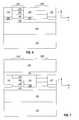
- FIG. 1shows a schematic diagram of an embodiment of a memory array comprised of a plurality of memory elements presented and formed in the context of the description provided herein.
- the circuit of memory array 5includes an xy grid with memory elements 30 electrically interconnected in series with isolation devices 25 on a portion of a chip.
- Address lines 10e.g., columns
- 20e.g., rows
- One purpose of the xy grid array of memory elements in combination with isolation devicesis to enable each discrete memory element to be read and written without interfering with the information stored in adjacent or remote memory elements of the array.
- a memory array such as memory device 5 of FIG. 1can be formed in a portion, including the entire portion, of a substrate.
- a typical substrateincludes a semiconductor substrate such as a silicon substrate.
- Other substratesincluding, but not limited to, substrates that contain ceramic material, organic material, or glass material as part of the infrastructure are also suitable.
- memory array 5can be fabricated over an area of the substrate at the wafer level and then the wafer reduced through singulation into discrete die or chips, some or all of the die or chips having a memory array formed thereon. Additional addressing circuitry (e.g., decoders, etc.) can be formed as known to those of skill in the art.
- FIGS. 2-14illustrate an embodiment of the fabrication of representative memory element 15 of FIG. 1 .
- FIG. 2depicts a portion of substrate 100 that is, for example, a semiconductor (e.g., silicon) substrate.
- a P-type dopantsuch as boron is introduced in portion 110 .
- a suitable concentration of P-type dopantis on the order of about 5 ⁇ 10 19 to 1 ⁇ 10 20 atoms per cubic centimeter (atoms/cm 3 ) rendering portion 110 of substrate 100 representatively P ++ .
- Overlying portion 110 of substrate 100is portion 120 of P-type epitaxial silicon.
- the dopant concentrationis on the order of about 10 16 to 10 17 atoms/cm 3 .
- FIG. 2also depicts shallow trench isolation (STI) structures 130 formed in epitaxial portion 120 of substrate 100 .
- STI structures 130serve, in one aspect, to define the z-direction thickness of a memory cell, with at this point only the z-direction thickness of a memory cell defined.
- memory cell z-direction regions 135 A and 135 Bare patterned as strips with the x-direction dimension greater than the z-direction dimension.
- STI structures 130serve to isolate individual memory elements from one another as well as associated circuit elements (e.g., transistor devices) formed in and on the substrate.
- Current state of the art photolithography techniques utilized to pattern STI structuresdefine the z-direction thickness of memory cell regions 135 A and 135 B can produce feature sizes (z-direction thickness) as small as 0.18 microns ( ⁇ m).
- FIG. 3depicts the structure of FIG. 2 after further fabrication operations in memory cell regions 135 A and 135 B.
- signal line material 140is N-type doped polysilicon formed by the introduction of, for example, phosphorous or arsenic to a concentration on the order of about 10 18 to 10 19 atoms/cm 3 (e.g., N + silicon).
- signal line material 140serves as an address line, a row line (e.g., row line 20 of FIG. 1 ).
- an isolation devicee.g., isolation device 25 of FIG. 1 ).
- the isolation deviceis a PN diode formed of N-type silicon portion 150 (e.g., dopant concentration on the order of about 10 14 to 10 18 atoms/cm 3 ) and P-type silicon portion 160 (e.g., dopant concentration on the order of about 10 19 to 10 20 atoms/cm 3 ).
- N-type silicon portion 150e.g., dopant concentration on the order of about 10 14 to 10 18 atoms/cm 3
- P-type silicon portion 160e.g., dopant concentration on the order of about 10 19 to 10 20 atoms/cm 3
- Such devicesinclude, but are not limited to, metal oxide semiconductor (MOS) devices.
- MOSmetal oxide semiconductor
- FIG. 4depicts the structure of FIG. 3 from an xy perspective after forming trenches 190 in epitaxial portion 120 of substrate 100 .
- Trenches 190are formed, in this example, orthogonal to STI structures 130 .
- Trenches 190define the x-direction thickness of a memory cell. According to current photolithographic techniques, a suitable feature size for the x-direction thickness is as small as 0.25 ⁇ m.
- FIG. 4also depicts memory cells 145 A and 145 B separated by trenches 190 , having a z-direction thickness defined by STI structures 130 and an x-direction thickness defined by trenches 190 .
- the definition of the x-direction thicknessinvolves, in one embodiment, an etch to the conductor or signal line 140 of the memory line stack to define memory cells 145 A and 145 B of memory cell region 135 A.
- the etchproceeds through the memory line stack to, in this example, a portion of conductor or signal line 140 .
- a timed etchcan be utilized to stop an etch at this point.
- N-type dopantis introduced at the base of each trench 190 to form pockets 200 having a dopant concentration on the order of about 10 18 to 10 20 atoms/cm 3 (e.g., N + region) between memory cells 145 A and 145 B.
- FIG. 5depicts an xz perspective of the structure of FIG. 4 with memory cells (e.g., memory cells 145 A and 145 B) separated by STI structures 130 and 132 .
- FIG. 6depicts the structure of FIG. 4 (i.e., an xy perspective) following the formation of a material of, in this example, refractory metal suicide such as cobalt silicide (CoSi 2 ) in a portion of p-type silicon portion 160 to define contact 170 .
- Contact 170serves as a low resistance material in the fabrication of peripheral circuitry (e.g., addressing circuitry) of the circuit structure o n the chip .
- FIG. 7depicts the structure of FIG. 6 after the introduction of masking material 180 .
- masking material 180serves, in one sense, as an etch stop for a subsequent etch operation.
- a suitable material for masking material 180is a dielectric material such as silicon nitride (Si 3 N 4 ).
- FIG. 7also depicts dielectric material 210 introduced over the structure to a thickness on the order of 100 ⁇ to 50,000 ⁇ sufficient to blanket memory cells 145 A and 145 B.
- dielectric material 210is SiO 2 .
- dielectric material 210is a material selected for its reduced thermal conductivity, ⁇ , preferably a thermal conductivity less than ⁇ SiO 2 , more preferably three to 10 times less ⁇ SiO 2 .
- SiO 2 and Si 3 N 4have ⁇ values on the order of 1.0.
- suitable materials for dielectric material 210include those materials that have ⁇ values less than 1.0.
- Certain high temperature polymers having ⁇ values less than 1.0include carbide materials, Aerogel, Xerogel ( ⁇ on the order of 0.1) and their derivatives.
- FIG. 8depicts the structure of FIG. 7, through the same cross-sectional view, after forming openings 220 through dielectric 210 and masking material 180 , exposing contact 170 .
- the formation of openings 220may be accomplished using etch patterning with an etchant(s) selective for etching dielectric material 210 and masking material 180 but not contact 170 (e.g., contact 170 serves as an etch stop).
- FIG. 9depicts the structure of FIG. 8, through the same cross-sectional view, depicting the conformal formation of electrode material 230 , utilizing ALD.
- ALDone reactant gas is introduced at a time.
- the first gasis “chemisorped” onto the surface of dielectric 210 , masking material 180 and contact 170 forming chemisorped layer 230 A.
- Excess gasis then purged and the second gas introduced. This gas reacts with the chemisorped layer 230 A, creating a monolayer of deposited film 230 B.
- Individual precursorsare pulsed onto surfaces in a sequential manner, without mixing precursors in the gas phase. Each individual precursor reacts with a surface to form an atomic layer in such a way that one layer forms at a time.
- the ALD processis self-limiting. That is, the surface reaction occurs and completes such that not more than one layer is deposited at a time, regardless of the number of molecules applied to the surface in an overdosing mode. Films are built up by introducing short bursts of gases in cycles. Conventional CVD processes typically operate above 500° C. while ALD is possible below 400° C., making it compatible with an industry trend to lower temperatures.
- the thin sidewall filmsdefine the x-axis dimension of the electrode (as will become more apparent in FIG. 11 ), the x-axis dimension being an important dimension in terms of device performance.
- the x-axis dimensiondetermines the required programming current for a reset, set, and read operation. The smaller the x-axis dimension that can be repeatedly reproduced, the smaller the required programming currents needed to operate the device. This is due to the smaller volume of programmable material whose phase is being changed and due to the reduced heat loss.
- electrode material 230(collectively 230 A, 230 B, . . . , 230 N atomic layers) has uniform film thickness, ultra-thin thickness (with respect to the x-axis dimension depicted in FIG. 11) and is a conformal film.
- electrode material 230has an x-axis dimension on the order of 10 angstroms to 1000 angstroms.
- electrode material 230is at least one of tungsten (W), tungsten nitride (WN), titanium nitride (TiN), titanium silicon nitride (TiSiN), and tantalum nitride (TaN).
- electrode material 230has a resistivity on the order of 0.001 to 0.05 ohm-cm resistivity.
- FIG. 10depicts the structure of FIG. 9 after the completion of conformal formation of electrode material 230 .
- the introductionis conformal in the sense that electrode material 230 is formed along the side walls and base of openings 220 (showing electrode material portions 230 A, 230 B and 230 C) such that electrode material 230 is in contact with contact 170 .
- the isolation of a single conductive pathmay be accomplished through an angled introduction of a dopant (i.e., angled away from electrode material 230 B).
- FIG. 11shows the structure after the introduction of dielectric material 250 into openings 220 .
- dielectric material 250is silicon dioxide (SiO 2 ).
- dielectric material 250is a material that has a thermal conductivity, ⁇ , that is less than the thermal conductivity of SiO 2 , ⁇ SiO 2 preferably three to 10 times less than ⁇ SiO 2 .
- ⁇thermal conductivity
- the structureis subjected to a planarization that removes the horizontal component of electrode material 230 . Suitable planarization techniques include those known to those of skill in the art, such as chemical or chemical-mechanical polish (CMP) techniques.
- CMPchemical or chemical-mechanical polish
- FIG. 12depicts the structure of FIG. 11, through the same cross-sectional view, after the optional conformal formation of barrier 275 utilizing ALD.
- electrode 230is selectively etched, ALD of barrier 275 is utilized to fill the area etched, and barrier 275 is then planarized.
- FIG. 13depicts the structure of FIG. 12, through the same cross-sectional view, after the formation and patterning of conductor 410 , barrier 408 , and programmable material 404 .
- the patterningcan be accomplished using conventional photolithographic and etch techniques. In this example, the etching proceeds through a portion of programmable material 404 , barrier 408 and conductor 410 , to the exclusion of barrier 275 , dielectric 210 and dielectric 250 .
- programmable material 404is a phase change material that has a property such that its physical state (e.g., crystalline, amorphous) can be modified with the application of an amount of energy (e.g., electrical energy, thermal energy).
- Chalcogenide materials having the general formulaare known to be suitable for this purpose.
- chalcogenide alloys suitable as programmable material 404include at least one element from column VI of the Periodic Table Of The Elements.
- Ge 2 Sb 2 Te 5is utilized as programmable material 404 .
- Other chalcogenide alloys utilized as programmable material 404include GaSb, InSb, InSe, Sb 2 Te 3 , GeTe, InSbTe, GaSeTe, SnSb 2 Te 4 , InSbGe, AgInSbTe, (GeSn)SbTe, GeSb(SeTe), and Te 81 Ge 15 Sb 2 S 2 .
- Barrier 408includes one of, for example, titanium (Ti) and titanium nitride (TiN). Barrier 408 serves, in one aspect, to inhibit diffusion between the volume of programmable material 404 and second signal line material overlying the volume of programmable material 404 (e.g., second electrode 10 ). Overlying barrier 408 is signal line material 410 .
- signal line material 410serves as an address line, a column line (e.g., column line 10 of FIG. 1 ).
- Signal line material 410is patterned to be, in one embodiment, generally orthogonal to signal line material 140 (column lines are orthogonal to row lines).
- Signal line material 410is, for example, an aluminum material, such as an aluminum alloy.
- FIG. 14shows the structure of FIG. 13 after forming dielectric material 412 on conductor 410 .
- Dielectric material 412is, for example, SiO 2 or other suitable material that is formed on conductor 410 to electronically isolate conductor 410 .
- dielectric material 412is planarized and a via is formed in a portion of the structure through dielectric material 412 , dielectric material 210 , and dielectric material 180 to contact 170 .
- the viais filled with conductive material 340 such as tungsten (W) and barrier material 350 such as a combination of titanium (Ti) and titanium nitride (TiN).
- conductive material 340such as tungsten (W)
- barrier material 350such as a combination of titanium (Ti) and titanium nitride (TiN).
- the structure shown in FIG. 14also shows additional signal line material 414 formed and patterned to mirror that of signal line material 140 (e.g., row line) formed on substrate 100 .
- Mirror conductor line material 414mirrors signal line material 140 and is coupled to signal line material 140 through the conductive via.
- mirror conductor line material 414serves, in one aspect, to reduce the resistance of signal line material 140 in a memory array, such as memory array 5 illustrated in FIG. 1.
- a suitable material for mirror conductor line material 414includes an aluminum material, such as an aluminum alloy.
- FIG. 15describes a method in forming a programmable memory device, having a structure similar to that depicted in FIG. 14, in accordance with an embodiment.
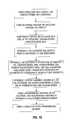
- system 700includes microprocessor 704 , input/output (I/O) port 706 , and memory 702 .
- Microprocessor 704 , I/O port 706 , and memory 702are connected by data bus 712 , address bus 716 and control bus 714 .
- Microprocessor 704fetches instructions or reads data from memory 702 by sending out an address on address bus 716 and a memory read signal on control bus 714 .
- Memory 702outputs the addressed instruction or data word to microprocessor 704 on data bus 712 .
- Microprocessor 704writes a data word to memory 702 by sending out an address on address bus 716 , sending out the data word on data bus 712 , and sending a memory write signal to memory 702 on control bus 714 .
- I/O port 706is utilized to couple to at least one of input device 708 and output device 710 .
Landscapes
- Engineering & Computer Science (AREA)
- Physics & Mathematics (AREA)
- Condensed Matter Physics & Semiconductors (AREA)
- General Physics & Mathematics (AREA)
- Manufacturing & Machinery (AREA)
- Computer Hardware Design (AREA)
- Microelectronics & Electronic Packaging (AREA)
- Power Engineering (AREA)
- Chemical & Material Sciences (AREA)
- Chemical Kinetics & Catalysis (AREA)
- General Chemical & Material Sciences (AREA)
- Semiconductor Memories (AREA)
Abstract
Description
Claims (5)
Priority Applications (4)
| Application Number | Priority Date | Filing Date | Title |
|---|---|---|---|
| US09/896,529US6511867B2 (en) | 2001-06-30 | 2001-06-30 | Utilizing atomic layer deposition for programmable device |
| TW091119537ATW586147B (en) | 2001-06-30 | 2002-08-28 | Utilizing atomic layer deposition for programmable device |
| US10/313,785US6919578B2 (en) | 2001-06-30 | 2002-12-06 | Utilizing atomic layer deposition for programmable device |
| US10/971,812US20050124157A1 (en) | 2001-06-30 | 2004-10-22 | Utilizing atomic layer deposition for programmable device |
Applications Claiming Priority (1)
| Application Number | Priority Date | Filing Date | Title |
|---|---|---|---|
| US09/896,529US6511867B2 (en) | 2001-06-30 | 2001-06-30 | Utilizing atomic layer deposition for programmable device |
Related Child Applications (1)
| Application Number | Title | Priority Date | Filing Date |
|---|---|---|---|
| US10/313,785DivisionUS6919578B2 (en) | 2001-06-30 | 2002-12-06 | Utilizing atomic layer deposition for programmable device |
Publications (2)
| Publication Number | Publication Date |
|---|---|
| US20030003634A1 US20030003634A1 (en) | 2003-01-02 |
| US6511867B2true US6511867B2 (en) | 2003-01-28 |
Family
ID=25406366
Family Applications (3)
| Application Number | Title | Priority Date | Filing Date |
|---|---|---|---|
| US09/896,529Expired - LifetimeUS6511867B2 (en) | 2001-06-30 | 2001-06-30 | Utilizing atomic layer deposition for programmable device |
| US10/313,785Expired - LifetimeUS6919578B2 (en) | 2001-06-30 | 2002-12-06 | Utilizing atomic layer deposition for programmable device |
| US10/971,812AbandonedUS20050124157A1 (en) | 2001-06-30 | 2004-10-22 | Utilizing atomic layer deposition for programmable device |
Family Applications After (2)
| Application Number | Title | Priority Date | Filing Date |
|---|---|---|---|
| US10/313,785Expired - LifetimeUS6919578B2 (en) | 2001-06-30 | 2002-12-06 | Utilizing atomic layer deposition for programmable device |
| US10/971,812AbandonedUS20050124157A1 (en) | 2001-06-30 | 2004-10-22 | Utilizing atomic layer deposition for programmable device |
Country Status (2)
| Country | Link |
|---|---|
| US (3) | US6511867B2 (en) |
| TW (1) | TW586147B (en) |
Cited By (267)
| Publication number | Priority date | Publication date | Assignee | Title |
|---|---|---|---|---|
| US20020116955A1 (en)* | 2001-02-19 | 2002-08-29 | Sumitomo Electric Industries, Ltd. | Method of forming soot preform |
| US20020138301A1 (en)* | 2001-03-22 | 2002-09-26 | Thanos Karras | Integration of a portal into an application service provider data archive and/or web based viewer |
| US20020168852A1 (en)* | 2001-05-11 | 2002-11-14 | Harshfield Steven T. | PCRAM memory cell and method of making same |
| US20030045049A1 (en)* | 2001-08-29 | 2003-03-06 | Campbell Kristy A. | Method of forming chalcogenide comprising devices |
| US20030047772A1 (en)* | 2001-03-15 | 2003-03-13 | Jiutao Li | Agglomeration elimination for metal sputter deposition of chalcogenides |
| US20030096497A1 (en)* | 2001-11-19 | 2003-05-22 | Micron Technology, Inc. | Electrode structure for use in an integrated circuit |
| US20030098461A1 (en)* | 2001-06-30 | 2003-05-29 | Lowrey Tyler A. | Utilizing atomic layer deposition for programmable device |
| US20030117831A1 (en)* | 2001-12-20 | 2003-06-26 | Glen Hush | Programmable conductor random access memory and a method for writing thereto |
| US20030128612A1 (en)* | 2002-01-04 | 2003-07-10 | John Moore | PCRAM rewrite prevention |
| US20030156463A1 (en)* | 2002-02-19 | 2003-08-21 | Casper Stephen L. | Programmable conductor random access memory and method for sensing same |
| US20030156468A1 (en)* | 2002-02-20 | 2003-08-21 | Campbell Kristy A. | Resistance variable 'on' memory |
| US20030155606A1 (en)* | 2002-02-15 | 2003-08-21 | Campbell Kristy A. | Method to alter chalcogenide glass for improved switching characteristics |
| US20030169625A1 (en)* | 2002-03-05 | 2003-09-11 | Glen Hush | Programmable conductor random access memory and method for sensing same |
| US6620724B1 (en)* | 2002-05-09 | 2003-09-16 | Infineon Technologies Ag | Low resistivity deep trench fill for DRAM and EDRAM applications |
| US20030173558A1 (en)* | 2002-03-14 | 2003-09-18 | Campbell Kristy A. | Methods and apparatus for resistance variable material cells |
| US20030193059A1 (en)* | 2002-04-10 | 2003-10-16 | Gilton Terry L. | Programmable conductor memory cell structure and method therefor |
| US20030194865A1 (en)* | 2002-04-10 | 2003-10-16 | Gilton Terry L. | Method of manufacture of programmable conductor memory |
| US20030193053A1 (en)* | 2002-04-10 | 2003-10-16 | Gilton Terry L. | Thin film diode integrated with chalcogenide memory cell |
| US20030212588A1 (en)* | 2002-05-09 | 2003-11-13 | Qwest Communications International Inc. | Systems and methods for creating network architecture planning tools |
| US20040007749A1 (en)* | 2002-07-10 | 2004-01-15 | Campbell Kristy A. | Assemblies displaying differential negative resistance |
| US20040007718A1 (en)* | 2001-08-30 | 2004-01-15 | Campbell Kristy A. | Stoichiometry for chalcogenide glasses useful for memory devices and method of formation |
| US20040029351A1 (en)* | 2002-01-31 | 2004-02-12 | Gilton Terry L. | Methods of forming non-volatile resistance variable devices and methods of forming silver selenide comprising structures |
| US20040038480A1 (en)* | 2002-08-22 | 2004-02-26 | Moore John T. | Method of manufacture of a PCRAM memory cell |
| US20040040837A1 (en)* | 2002-08-29 | 2004-03-04 | Mcteer Allen | Method of forming chalcogenide sputter target |
| US20040043553A1 (en)* | 2002-06-06 | 2004-03-04 | Jiutao Li | Elimination of dendrite formation during metal/chalcogenide glass deposition |
| US20040043245A1 (en)* | 2002-08-29 | 2004-03-04 | Moore John T. | Method to control silver concentration in a resistance variable memory element |
| US20040040835A1 (en)* | 2002-08-29 | 2004-03-04 | Jiutao Li | Silver selenide film stoichiometry and morphology control in sputter deposition |
| US20040053461A1 (en)* | 2002-08-29 | 2004-03-18 | Moore John T. | Graded GexSe100-x concentration in PCRAM |
| US6750066B1 (en)* | 2002-04-08 | 2004-06-15 | Advanced Micro Devices, Inc. | Precision high-K intergate dielectric layer |
| US20040124406A1 (en)* | 2001-08-29 | 2004-07-01 | Campbell Kristy A. | Method of forming non-volatile resistance variable devices, method of forming a programmable memory cell of memory circuitry, and a non-volatile resistance variable device |
| US20040130598A1 (en)* | 2002-07-10 | 2004-07-08 | Canon Kabushiki Kaisha | Ink jet record head |
| US20040145941A1 (en)* | 2002-10-15 | 2004-07-29 | Rust Thomas F | Phase change media for high density data storage |
| US20040157417A1 (en)* | 2002-08-29 | 2004-08-12 | Moore John T. | Methods to form a memory cell with metal-rich metal chalcogenide |
| US20040161874A1 (en)* | 2001-03-01 | 2004-08-19 | Moore John T. | Method of forming a non-volatile resistance variable device, and non-volatile resistance variable device |
| US20040175859A1 (en)* | 2002-08-29 | 2004-09-09 | Campbell Kristy A. | Single polarity programming of a PCRAM structure |
| US20040180533A1 (en)* | 2003-03-14 | 2004-09-16 | Li Li | Method for filling via with metal |
| US20040192006A1 (en)* | 2002-02-20 | 2004-09-30 | Campbell Kristy A. | Layered resistance variable memory device and method of fabrication |
| US20040202016A1 (en)* | 2003-04-10 | 2004-10-14 | Campbell Kristy A. | Differential negative resistance memory |
| US6809362B2 (en) | 2002-02-20 | 2004-10-26 | Micron Technology, Inc. | Multiple data state memory cell |
| US20040211957A1 (en)* | 2002-08-29 | 2004-10-28 | Moore John T. | Method and apparatus for controlling metal doping of a chalcogenide memory element |
| US6813178B2 (en) | 2003-03-12 | 2004-11-02 | Micron Technology, Inc. | Chalcogenide glass constant current device, and its method of fabrication and operation |
| US20040235235A1 (en)* | 2002-06-06 | 2004-11-25 | Jiutao Li | Co-sputter deposition of metal-doped chalcogenides |
| US20040232467A1 (en)* | 1999-12-09 | 2004-11-25 | Hayashi Otsuki | TiSiN film forming method, diffusion barrier TiSiN film, semiconductor device, method of fabricating the same and TiSiN film forming system |
| US6833559B2 (en) | 2001-02-08 | 2004-12-21 | Micron Technology, Inc. | Non-volatile resistance variable device |
| US20040264234A1 (en)* | 2003-06-25 | 2004-12-30 | Moore John T. | PCRAM cell operation method to control on/off resistance variation |
| US20050018509A1 (en)* | 2001-11-20 | 2005-01-27 | Glen Hush | Complementary bit resistance memory sensor and method of operation |
| US20050017233A1 (en)* | 2003-07-21 | 2005-01-27 | Campbell Kristy A. | Performance PCRAM cell |
| US20050026433A1 (en)* | 2001-08-30 | 2005-02-03 | Jiutao Li | Integrated circuit device and fabrication using metal-doped chalcogenide materials |
| US20050054207A1 (en)* | 2002-08-29 | 2005-03-10 | Micron Technology, Inc. | Plasma etching methods and methods of forming memory devices comprising a chalcogenide comprising layer received operably proximate conductive electrodes |
| US20050059187A1 (en)* | 2003-09-17 | 2005-03-17 | Gilton Terry L. | Non-volatile memory structure |
| US20050062074A1 (en)* | 2002-08-09 | 2005-03-24 | Macronix International Co., Ltd. | Spacer chalcogenide memory method |
| US20050069641A1 (en)* | 2003-09-30 | 2005-03-31 | Tokyo Electron Limited | Method for depositing metal layers using sequential flow deposition |
| US20050069632A1 (en)* | 2003-09-30 | 2005-03-31 | Tokyo Electron Limited | Method of forming a metal layer using an intermittent precursor gas flow process |
| US6894304B2 (en) | 2001-08-27 | 2005-05-17 | Micron Technology, Inc. | Apparatus and method for dual cell common electrode PCRAM memory device |
| US20050122771A1 (en)* | 2003-12-05 | 2005-06-09 | Bomy Chen | Memory device and method of operating same |
| US20050162883A1 (en)* | 2002-08-08 | 2005-07-28 | Hasan Nejad | Columnar 1T-nMemory cell structure and its method of formation and operation |
| US20050162907A1 (en)* | 2004-01-28 | 2005-07-28 | Campbell Kristy A. | Resistance variable memory elements based on polarized silver-selenide network growth |
| US20050167689A1 (en)* | 2004-01-29 | 2005-08-04 | Campbell Kristy A. | Non-volatile zero field splitting resonance memory |
| US20050202588A1 (en)* | 2004-03-10 | 2005-09-15 | Brooks Joseph F. | Method of forming a chalcogenide material containing device |
| US20050201174A1 (en)* | 2004-03-10 | 2005-09-15 | Klein Dean A. | Power management control and controlling memory refresh operations |
| US6951805B2 (en) | 2001-08-01 | 2005-10-04 | Micron Technology, Inc. | Method of forming integrated circuitry, method of forming memory circuitry, and method of forming random access memory circuitry |
| US20050232061A1 (en)* | 2004-04-16 | 2005-10-20 | Rust Thomas F | Systems for writing and reading highly resolved domains for high density data storage |
| US20050232004A1 (en)* | 2004-04-16 | 2005-10-20 | Rust Thomas F | Methods for erasing bit cells in a high density data storage device |
| US20050243660A1 (en)* | 2004-04-16 | 2005-11-03 | Rust Thomas F | Methods for erasing bit cells in a high density data storage device |
| US20050243592A1 (en)* | 2004-04-16 | 2005-11-03 | Rust Thomas F | High density data storage device having eraseable bit cells |
| US20060011910A1 (en)* | 2004-07-19 | 2006-01-19 | Micron Technology, Inc. | PCRAM device with switching glass layer |
| US20060012008A1 (en)* | 2004-07-19 | 2006-01-19 | Campbell Kristy A | Resistance variable memory device and method of fabrication |
| US20060035403A1 (en)* | 2004-08-12 | 2006-02-16 | Campbell Kristy A | PCRAM device with switching glass layer |
| US20060033094A1 (en)* | 2004-08-12 | 2006-02-16 | Campbell Kristy A | Resistance variable memory with temperature tolerant materials |
| US20060044906A1 (en)* | 2004-09-01 | 2006-03-02 | Ethan Williford | Sensing of resistance variable memory devices |
| US7010644B2 (en) | 2002-08-29 | 2006-03-07 | Micron Technology, Inc. | Software refreshed memory device and method |
| US20060110878A1 (en)* | 2004-11-22 | 2006-05-25 | Macronix International Co., Ltd. | Side wall active pin memory and manufacturing method |
| US20060124916A1 (en)* | 2004-12-09 | 2006-06-15 | Macronix International Co., Ltd. | Self-aligned small contact phase-change memory method and device |
| US20060131556A1 (en)* | 2004-12-22 | 2006-06-22 | Micron Technology, Inc. | Small electrode for resistance variable devices |
| US20060131555A1 (en)* | 2004-12-22 | 2006-06-22 | Micron Technology, Inc. | Resistance variable devices with controllable channels |
| US20060237707A1 (en)* | 2005-04-22 | 2006-10-26 | Micron Technology, Inc. | Memory array for increased bit density and method of forming the same |
| US20060256640A1 (en)* | 2005-05-16 | 2006-11-16 | Micron Technology, Inc. | Power circuits for reducing a number of power supply voltage taps required for sensing a resistive memory |
| US20060270099A1 (en)* | 2001-08-29 | 2006-11-30 | Micron Technology, Inc. | Method of forming non-volatile resistance variable devices and method of forming a programmable memory cell of memory circuitry |
| US20060284214A1 (en)* | 2005-06-17 | 2006-12-21 | Macronix International Co., Ltd. | Thin film fuse phase change cell with thermal isolation layer and manufacturing method |
| US20060284158A1 (en)* | 2005-06-17 | 2006-12-21 | Macronix International Co., Ltd. | Self-aligned, embedded phase change ram and manufacturing method |
| US20060286709A1 (en)* | 2005-06-17 | 2006-12-21 | Macronix International Co., Ltd. | Manufacturing methods for thin film fuse phase change ram |
| US20060284157A1 (en)* | 2005-06-17 | 2006-12-21 | Macronix International Co., Ltd. | Thin film plate phase change RAM circuit and manufacturing method |
| US20060286743A1 (en)* | 2005-06-17 | 2006-12-21 | Macronix International Co., Ltd. | Method for Manufacturing a Narrow Structure on an Integrated Circuit |
| US20060284279A1 (en)* | 2005-06-17 | 2006-12-21 | Macronix International Co., Ltd. | Thin film fuse phase change RAM and manufacturing method |
| US20060291271A1 (en)* | 2005-06-24 | 2006-12-28 | Nanochip, Inc. | High density data storage devices having servo indicia formed in a patterned media |
| US20070008864A1 (en)* | 2005-06-24 | 2007-01-11 | Nanochip, Inc. | Patterned media for a high density data storage device |
| US20070006455A1 (en)* | 2005-06-24 | 2007-01-11 | Nanochip, Inc. | Methods for forming high density data storage devices with read/write probes with hollow or reinforced tips |
| US20070008768A1 (en)* | 2005-07-08 | 2007-01-11 | Micron Technology, Inc. | Process for erasing chalcogenide variable resistance memory bits |
| US20070007505A1 (en)* | 2005-07-07 | 2007-01-11 | Honeywell International Inc. | Chalcogenide PVD components |
| US20070008865A1 (en)* | 2005-07-08 | 2007-01-11 | Nanochip, Inc. | High density data storage devices with polarity-dependent memory switching media |
| US20070008867A1 (en)* | 2005-07-08 | 2007-01-11 | Nanochip, Inc. | High density data storage devices with a lubricant layer comprised of a field of polymer chains |
| US20070010054A1 (en)* | 2005-07-08 | 2007-01-11 | Nanochip, Inc. | Method for forming patterned media for a high density data storage device |
| US20070007506A1 (en)* | 2002-02-20 | 2007-01-11 | Micron Technology, Inc. | Layered resistance variable memory device and method of fabrication |
| US20070008866A1 (en)* | 2005-07-08 | 2007-01-11 | Nanochip, Inc. | Methods for writing and reading in a polarity-dependent memory switch media |
| US20070023744A1 (en)* | 2005-08-01 | 2007-02-01 | Micron Technology, Inc. | Resistance variable memory device with sputtered metal-chalcogenide region and method of fabrication |
| US20070030554A1 (en)* | 2005-08-02 | 2007-02-08 | Micron Technology, Inc. | Method and apparatus for providing color changing thin film material |
| US20070029537A1 (en)* | 2005-08-02 | 2007-02-08 | Micron Technology, Inc. | Phase change memory cell and method of formation |
| US20070037316A1 (en)* | 2005-08-09 | 2007-02-15 | Micron Technology, Inc. | Memory cell contact using spacers |
| US20070035990A1 (en)* | 2005-08-15 | 2007-02-15 | Micron Technology, Inc. | Method and apparatus providing a cross-point memory array using a variable resistance memory cell and capacitance |
| US20070034921A1 (en)* | 2005-08-09 | 2007-02-15 | Micron Technology, Inc. | Access transistor for memory device |
| US20070047297A1 (en)* | 2005-08-31 | 2007-03-01 | Campbell Kristy A | Resistance variable memory element with threshold device and method of forming the same |
| US20070059882A1 (en)* | 2005-04-22 | 2007-03-15 | Micron Technology, Inc. | Memory elements having patterned electrodes and method of forming the same |
| US7205234B2 (en) | 2004-02-05 | 2007-04-17 | Taiwan Semiconductor Manufacturing Company, Ltd. | Method of forming metal silicide |
| US20070090354A1 (en)* | 2005-08-11 | 2007-04-26 | Micron Technology, Inc. | Chalcogenide-based electrokinetic memory element and method of forming the same |
| US20070099332A1 (en)* | 2005-07-07 | 2007-05-03 | Honeywell International Inc. | Chalcogenide PVD components and methods of formation |
| US20070111429A1 (en)* | 2005-11-14 | 2007-05-17 | Macronix International Co., Ltd. | Method of manufacturing a pipe shaped phase change memory |
| US20070108429A1 (en)* | 2005-11-14 | 2007-05-17 | Macronix International Co., Ltd. | Pipe shaped phase change memory |
| US20070109836A1 (en)* | 2005-11-15 | 2007-05-17 | Macronix International Co., Ltd. | Thermally insulated phase change memory device and manufacturing method |
| US20070109843A1 (en)* | 2005-11-15 | 2007-05-17 | Macronix International Co., Ltd. | Phase Change Memory Device and Manufacturing Method |
| US20070121363A1 (en)* | 2005-11-28 | 2007-05-31 | Macronix International Co., Ltd. | Phase Change Memory Cell and Manufacturing Method |
| US20070126040A1 (en)* | 2005-11-21 | 2007-06-07 | Hsiang-Lan Lung | Vacuum cell thermal isolation for a phase change memory device |
| US20070131922A1 (en)* | 2005-12-13 | 2007-06-14 | Macronix International Co., Ltd. | Thin Film Fuse Phase Change Cell with Thermal Isolation Pad and Manufacturing Method |
| US20070131980A1 (en)* | 2005-11-21 | 2007-06-14 | Lung Hsiang L | Vacuum jacket for phase change memory element |
| US20070155172A1 (en)* | 2005-12-05 | 2007-07-05 | Macronix International Co., Ltd. | Manufacturing Method for Phase Change RAM with Electrode Layer Process |
| US20070154847A1 (en)* | 2005-12-30 | 2007-07-05 | Macronix International Co., Ltd. | Chalcogenide layer etching method |
| US20070158690A1 (en)* | 2006-01-09 | 2007-07-12 | Macronix International Co., Ltd. | Programmable Resistive RAM and Manufacturing Method |
| US20070158862A1 (en)* | 2005-11-21 | 2007-07-12 | Hsiang-Lan Lung | Vacuum jacketed electrode for phase change memory element |
| US20070161186A1 (en)* | 2006-01-09 | 2007-07-12 | Macronix International Co., Ltd. | Programmable Resistive RAM and Manufacturing Method |
| US20070158645A1 (en)* | 2006-01-11 | 2007-07-12 | Macronix International Co., Ltd. | Self-align planerized bottom electrode phase change memory and manufacturing method |
| US20070158633A1 (en)* | 2005-12-27 | 2007-07-12 | Macronix International Co., Ltd. | Method for Forming Self-Aligned Thermal Isolation Cell for a Variable Resistance Memory Array |
| US20070158632A1 (en)* | 2006-01-09 | 2007-07-12 | Macronix International Co., Ltd. | Method for Fabricating a Pillar-Shaped Phase Change Memory Element |
| US20070165444A1 (en)* | 1998-12-18 | 2007-07-19 | Nanochip, Inc. | Devices and methods of detecting movement between media and probe tip in a probe data storage system |
| US20070173019A1 (en)* | 2006-01-09 | 2007-07-26 | Macronix International Co., Ltd. | Programmable Resistive Ram and Manufacturing Method |
| US20070173063A1 (en)* | 2006-01-24 | 2007-07-26 | Macronix International Co., Ltd. | Self-aligned manufacturing method, and manufacturing method for thin film fuse phase change ram |
| US20070176261A1 (en)* | 2006-01-30 | 2007-08-02 | Macronix International Co., Ltd. | Vertical Side Wall Active Pin Structures in a Phase Change Memory and Manufacturing Methods |
| US7269044B2 (en) | 2005-04-22 | 2007-09-11 | Micron Technology, Inc. | Method and apparatus for accessing a memory array |
| US20070241371A1 (en)* | 2006-04-17 | 2007-10-18 | Macronix International Co., Ltd. | Memory device and manufacturing method |
| US20070257300A1 (en)* | 2006-05-05 | 2007-11-08 | Macronix International Co., Ltd. | Structures and Methods of a Bistable Resistive Random Access Memory |
| US7294527B2 (en) | 2002-08-29 | 2007-11-13 | Micron Technology Inc. | Method of forming a memory cell |
| US20070262388A1 (en)* | 2006-05-09 | 2007-11-15 | Macronix International Co., Ltd. | Bridge Resistance Random Access Memory Device and Method With A Singular Contact Structure |
| US20070281420A1 (en)* | 2006-05-30 | 2007-12-06 | Macronix International Co., Ltd. | Resistor random access memory cell with reduced active area and reduced contact areas |
| US20070278529A1 (en)* | 2006-05-30 | 2007-12-06 | Macronix International Co., Ltd. | Resistor random access memory cell with l-shaped electrode |
| US20080001075A1 (en)* | 2006-06-15 | 2008-01-03 | Nanochip, Inc. | Memory stage for a probe storage device |
| US7317200B2 (en) | 2005-02-23 | 2008-01-08 | Micron Technology, Inc. | SnSe-based limited reprogrammable cell |
| US7319057B2 (en)* | 2001-10-30 | 2008-01-15 | Ovonyx, Inc. | Phase change material memory device |
| US20080014676A1 (en)* | 2006-07-12 | 2008-01-17 | Macronix International Co., Ltd. | Method for Making a Pillar-Type Phase Change Memory Element |
| US20080043520A1 (en)* | 2006-02-07 | 2008-02-21 | Chen Shih H | I-shaped phase change memory cell with thermal isolation |
| US7336524B2 (en) | 2002-10-15 | 2008-02-26 | Nanochip, Inc. | Atomic probes and media for high density data storage |
| US20080061341A1 (en)* | 2006-09-11 | 2008-03-13 | Macronix International Co., Ltd. | Memory Device Having Wide Area Phase Change Element and Small Electrode Contact Area |
| US20080094885A1 (en)* | 2006-10-24 | 2008-04-24 | Macronix International Co., Ltd. | Bistable Resistance Random Access Memory Structures with Multiple Memory Layers and Multilevel Memory States |
| US20080096375A1 (en)* | 2006-10-18 | 2008-04-24 | Macronix International Co., Ltd. | Method for Making Memory Cell Device |
| US20080096341A1 (en)* | 2006-10-24 | 2008-04-24 | Macronix International Co., Ltd. | Method for Manufacturing a Resistor Random Access Memory with Reduced Active Area and Reduced Contact Areas |
| US20080099791A1 (en)* | 2006-10-04 | 2008-05-01 | Macronix International Co., Ltd. | Memory Cell Device with Circumferentially-Extending Memory Element |
| US20080105901A1 (en)* | 2006-11-07 | 2008-05-08 | Kamal Tabatabaie | Atomic layer deposition in the formation of gate structures for iii-v semiconductor |
| US20080106923A1 (en)* | 2006-10-24 | 2008-05-08 | Macronix International Co., Ltd. | Phase Change Memory Cells with Dual Access Devices |
| US20080112878A1 (en)* | 2006-11-09 | 2008-05-15 | Honeywell International Inc. | Alloy casting apparatuses and chalcogenide compound synthesis methods |
| US7379412B2 (en) | 2004-04-16 | 2008-05-27 | Nanochip, Inc. | Methods for writing and reading highly resolved domains for high density data storage |
| US20080121861A1 (en)* | 2006-08-16 | 2008-05-29 | Macronix International Co., Ltd. | Self-Aligned Structure and Method for Confining a Melting Point in a Resistor Random Access Memory |
| US7385868B2 (en) | 2003-07-08 | 2008-06-10 | Micron Technology, Inc. | Method of refreshing a PCRAM memory device |
| US20080137400A1 (en)* | 2006-12-06 | 2008-06-12 | Macronix International Co., Ltd. | Phase Change Memory Cell with Thermal Barrier and Method for Fabricating the Same |
| US20080135824A1 (en)* | 2006-12-07 | 2008-06-12 | Macronix International Co., Ltd. | Method and Structure of a Multi-Level Cell Resistance Random Access Memory with Metal Oxides |
| US20080138931A1 (en)* | 2006-12-06 | 2008-06-12 | Macronix International Co., Ltd. | Method for Making a Self-Converged Void and Bottom Electrode for Memoery Cell |
| US20080138929A1 (en)* | 2006-12-06 | 2008-06-12 | Macronix International Co., Ltd. | Method for Making a Self-Converged Memory Material Element for Memory Cell |
| US7388771B2 (en) | 2006-10-24 | 2008-06-17 | Macronix International Co., Ltd. | Methods of operating a bistable resistance random access memory with multiple memory layers and multilevel memory states |
| US20080144353A1 (en)* | 2006-12-13 | 2008-06-19 | Macronix International Co., Ltd. | Method, Apparatus and Computer Program Product for Read Before Programming Process on Programmable Resistive Memory Cell |
| US20080142984A1 (en)* | 2006-12-15 | 2008-06-19 | Macronix International Co., Ltd. | Multi-Layer Electrode Structure |
| US20080157053A1 (en)* | 2006-12-28 | 2008-07-03 | Macronix International Co., Ltd. | Resistor Random Access Memory Cell Device |
| US20080165570A1 (en)* | 2007-01-05 | 2008-07-10 | Macronix International Co., Ltd. | Current Compliant Sensing Architecture for Multilevel Phase Change Memory |
| US20080175033A1 (en)* | 2007-01-19 | 2008-07-24 | Nanochip, Inc. | Method and system for improving domain stability in a ferroelectric media |
| US20080185730A1 (en)* | 2007-02-02 | 2008-08-07 | Macronix International Co., Ltd. | Memory cell device with coplanar electrode surface and method |
| US20080186755A1 (en)* | 2007-02-05 | 2008-08-07 | Macronix International Co., Ltd. | Memory cell device and programming methods |
| US20080186761A1 (en)* | 2007-02-07 | 2008-08-07 | Macronix International Co., Ltd. | Memory Cell with Separate Read and Program Paths |
| US20080191187A1 (en)* | 2007-02-12 | 2008-08-14 | Macronix International Co., Ltd. | Method for manufacturing a phase change memory device with pillar bottom electrode |
| US20080192534A1 (en)* | 2007-02-08 | 2008-08-14 | Macronix International Co., Ltd. | Memory element with reduced-current phase change element |
| US20080191186A1 (en)* | 2007-02-14 | 2008-08-14 | Macronix International Co., Ltd. | Phase change memory cell with filled sidewall memory element and method for fabricating the same |
| US7414258B2 (en) | 2005-11-16 | 2008-08-19 | Macronix International Co., Ltd. | Spacer electrode small pin phase change memory RAM and manufacturing method |
| US20080197333A1 (en)* | 2007-02-21 | 2008-08-21 | Macronix International Co., Ltd. | Programmable Resistive Memory Cell with Self-Forming Gap |
| US20080197334A1 (en)* | 2007-02-21 | 2008-08-21 | Macronix International Co., Ltd. | Phase Change Memory Cell with Heater and Method for Fabricating the Same |
| US20080203375A1 (en)* | 2007-02-27 | 2008-08-28 | Macronix International Co., Ltd. | Memory Cell with Memory Element Contacting Ring-Shaped Upper End of Bottom Electrode |
| US7423300B2 (en) | 2006-05-24 | 2008-09-09 | Macronix International Co., Ltd. | Single-mask phase change memory element |
| US20080233672A1 (en)* | 2007-03-20 | 2008-09-25 | Nanochip, Inc. | Method of integrating mems structures and cmos structures using oxide fusion bonding |
| US7433226B2 (en) | 2007-01-09 | 2008-10-07 | Macronix International Co., Ltd. | Method, apparatus and computer program product for read before programming process on multiple programmable resistive memory cell |
| US7440315B2 (en) | 2007-01-09 | 2008-10-21 | Macronix International Co., Ltd. | Method, apparatus and computer program product for stepped reset programming process on programmable resistive memory cell |
| US20080258125A1 (en)* | 2007-04-17 | 2008-10-23 | Micron Technology, Inc. | Resistive memory cell fabrication methods and devices |
| US20080258126A1 (en)* | 2007-04-17 | 2008-10-23 | Macronix International Co., Ltd. | Memory Cell Sidewall Contacting Side Electrode |
| US20080266933A1 (en)* | 2007-04-24 | 2008-10-30 | Macronix International Co., Ltd. | Method and Apparatus for Refreshing Programmable Resistive Memory |
| US20080266940A1 (en)* | 2005-11-21 | 2008-10-30 | Erh-Kun Lai | Air Cell Thermal Isolation for a Memory Array Formed of a Programmable Resistive Material |
| US7450411B2 (en) | 2005-11-15 | 2008-11-11 | Macronix International Co., Ltd. | Phase change memory device and manufacturing method |
| US20090032796A1 (en)* | 2007-07-31 | 2009-02-05 | Macronix International Co., Ltd. | Phase change memory bridge cell |
| US20090034323A1 (en)* | 2007-08-02 | 2009-02-05 | Macronix International Co., Ltd. | Phase change memory with dual word lines and source lines and method of operating same |
| US20090057644A1 (en)* | 2007-08-24 | 2009-03-05 | Samsung Electronics Co., Ltd | Phase-change memory units, methods of forming the phase-change memory units, phase-change memory devices having the phase-change memory units and methods of manufacturung the phase-change memory devices |
| US20090072216A1 (en)* | 2007-09-14 | 2009-03-19 | Macronix International Co., Ltd. | Phase change memory cell array with self-converged bottom electrode and method for manufacturing |
| US20090072215A1 (en)* | 2007-09-14 | 2009-03-19 | Macronix International Co., Ltd. | Phase change memory cell in via array with self-aligned, self-converged bottom electrode and method for manufacturing |
| US7507986B2 (en) | 2005-11-21 | 2009-03-24 | Macronix International Co., Ltd. | Thermal isolation for an active-sidewall phase change memory cell |
| US20090087550A1 (en)* | 2007-09-27 | 2009-04-02 | Tokyo Electron Limited | Sequential flow deposition of a tungsten silicide gate electrode film |
| US20090095948A1 (en)* | 2007-10-12 | 2009-04-16 | Macronix International Co., Ltd. | Programmable Resistive Memory with Diode Structure |
| US7521364B2 (en) | 2005-12-02 | 2009-04-21 | Macronix Internation Co., Ltd. | Surface topology improvement method for plug surface areas |
| US20090122588A1 (en)* | 2007-11-14 | 2009-05-14 | Macronix International Co., Ltd. | Phase change memory cell including a thermal protect bottom electrode and manufacturing methods |
| US7534647B2 (en) | 2005-06-17 | 2009-05-19 | Macronix International Co., Ltd. | Damascene phase change RAM and manufacturing method |
| US7535756B2 (en) | 2007-01-31 | 2009-05-19 | Macronix International Co., Ltd. | Method to tighten set distribution for PCRAM |
| US20090147564A1 (en)* | 2007-12-07 | 2009-06-11 | Macronix International Co., Ltd. | Phase change memory cell having interface structures with essentially equal thermal impedances and manufacturing methods |
| US20090159867A1 (en)* | 2007-12-20 | 2009-06-25 | Savransky Semyon D | Phase change memory with layered insulator |
| US20090184310A1 (en)* | 2008-01-18 | 2009-07-23 | Macronix International Co., Ltd. | Memory cell with memory element contacting an inverted t-shaped bottom electrode |
| US20090189138A1 (en)* | 2008-01-28 | 2009-07-30 | Macronix International Co., Ltd. | Fill-in etching free pore device |
| US20090242880A1 (en)* | 2008-03-25 | 2009-10-01 | Macronix International Co., Ltd. | Thermally stabilized electrode structure |
| US7599217B2 (en) | 2005-11-22 | 2009-10-06 | Macronix International Co., Ltd. | Memory cell device and manufacturing method |
| US20090261313A1 (en)* | 2008-04-22 | 2009-10-22 | Macronix International Co., Ltd. | Memory cell having a buried phase change region and method for fabricating the same |
| US20090261316A1 (en)* | 2006-08-29 | 2009-10-22 | Jun Liu | Enhanced memory density resistance variable memory cells, arrays, devices and systems including the same, and methods of fabrication |
| US20090279350A1 (en)* | 2008-05-07 | 2009-11-12 | Macronix International Co., Ltd. | Bipolar switching of phase change device |
| US20090294028A1 (en)* | 2008-06-03 | 2009-12-03 | Nanochip, Inc. | Process for fabricating high density storage device with high-temperature media |
| US20090309087A1 (en)* | 2008-06-12 | 2009-12-17 | Macronix International Co., Ltd. | Phase change memory cell having top and bottom sidewall contacts |
| US7635855B2 (en) | 2005-11-15 | 2009-12-22 | Macronix International Co., Ltd. | I-shaped phase change memory cell |
| US7639527B2 (en) | 2008-01-07 | 2009-12-29 | Macronix International Co., Ltd. | Phase change memory dynamic resistance test and manufacturing methods |
| US20090323409A1 (en)* | 2008-06-27 | 2009-12-31 | Macronix International Co., Ltd. | Methods for high speed reading operation of phase change memory and device employing same |
| US20100019215A1 (en)* | 2008-07-22 | 2010-01-28 | Macronix International Co., Ltd. | Mushroom type memory cell having self-aligned bottom electrode and diode access device |
| US7663135B2 (en) | 2007-01-31 | 2010-02-16 | Macronix International Co., Ltd. | Memory cell having a side electrode contact |
| US20100039919A1 (en)* | 2008-08-15 | 2010-02-18 | Nanochip, Inc. | Cantilever Structure for Use in Seek-and-Scan Probe Storage |
| US20100046285A1 (en)* | 2008-08-19 | 2010-02-25 | Macronix International Co., Ltd. | Multiple phase change materials in an integrated circuit for system on a chip application |
| US20100067285A1 (en)* | 2008-09-12 | 2010-03-18 | Macronix International Co., Ltd. | Novel sensing circuit for pcram applications |
| US7682868B2 (en) | 2006-12-06 | 2010-03-23 | Macronix International Co., Ltd. | Method for making a keyhole opening during the manufacture of a memory cell |
| US7688619B2 (en) | 2005-11-28 | 2010-03-30 | Macronix International Co., Ltd. | Phase change memory cell and manufacturing method |
| US20100084624A1 (en)* | 2008-10-02 | 2010-04-08 | Macronix International Co., Ltd. | Dielectric mesh isolated phase change structure for phase change memory |
| US7696503B2 (en) | 2005-06-17 | 2010-04-13 | Macronix International Co., Ltd. | Multi-level memory cell having phase change element and asymmetrical thermal boundary |
| US7696506B2 (en) | 2006-06-27 | 2010-04-13 | Macronix International Co., Ltd. | Memory cell with memory material insulation and manufacturing method |
| US7701750B2 (en) | 2008-05-08 | 2010-04-20 | Macronix International Co., Ltd. | Phase change device having two or more substantial amorphous regions in high resistance state |
| US20100110778A1 (en)* | 2008-11-06 | 2010-05-06 | Macronix International Co., Ltd. | Phase change memory program method without over-reset |
| US20100117048A1 (en)* | 2008-11-07 | 2010-05-13 | Macronix International Co., Ltd. | Memory cell access device having a pn-junction with polycrystalline and single-crystal semiconductor regions |
| US20100171086A1 (en)* | 2009-01-07 | 2010-07-08 | Macronix International Co., Ltd. | Integrated circuit memory with single crystal silicon on silicide driver and manufacturing method |
| US7755076B2 (en) | 2007-04-17 | 2010-07-13 | Macronix International Co., Ltd. | 4F2 self align side wall active phase change memory |
| US20100177559A1 (en)* | 2009-01-12 | 2010-07-15 | Macronix International Co., Ltd. | Method for setting pcram devices |
| US20100176362A1 (en)* | 2009-01-13 | 2010-07-15 | Macronix International Co., Ltd. | Polysilicon plug bipolar transistor for phase change memory |
| US20100177553A1 (en)* | 2009-01-14 | 2010-07-15 | Macronix International Co., Ltd. | Rewritable memory device |
| US7777215B2 (en) | 2007-07-20 | 2010-08-17 | Macronix International Co., Ltd. | Resistive memory structure with buffer layer |
| US7786461B2 (en) | 2007-04-03 | 2010-08-31 | Macronix International Co., Ltd. | Memory structure with reduced-size memory element between memory material portions |
| US20100270529A1 (en)* | 2009-04-27 | 2010-10-28 | Macronix International Co., Ltd. | Integrated circuit 3d phase change memory array and manufacturing method |
| US7825398B2 (en) | 2008-04-07 | 2010-11-02 | Macronix International Co., Ltd. | Memory cell having improved mechanical stability |
| US20100276654A1 (en)* | 2009-04-30 | 2010-11-04 | Macronix International Co., Ltd. | Low Operational Current Phase Change Memory Structures |
| US20100290271A1 (en)* | 2009-05-15 | 2010-11-18 | Macronix International Co., Ltd. | One-transistor, one-resistor, one-capacitor phase change memory |
| US20100295123A1 (en)* | 2009-05-22 | 2010-11-25 | Macronix International Co., Ltd. | Phase Change Memory Cell Having Vertical Channel Access Transistor |
| US20100314601A1 (en)* | 2009-06-15 | 2010-12-16 | Macronix International Co., Ltd. | Phase change memory having stabilized microstructure and manufacturing method |
| US20100321987A1 (en)* | 2009-06-22 | 2010-12-23 | Macronix International Co., Ltd. | Memory device and method for sensing and fixing margin cells |
| US20100328996A1 (en)* | 2009-06-25 | 2010-12-30 | Macronix International Co., Ltd. | Phase change memory having one or more non-constant doping profiles |
| US20100328995A1 (en)* | 2009-06-25 | 2010-12-30 | Macronix International Co., Ltd. | Methods and apparatus for reducing defect bits in phase change memory |
| US7869270B2 (en) | 2008-12-29 | 2011-01-11 | Macronix International Co., Ltd. | Set algorithm for phase change memory cell |
| US20110012083A1 (en)* | 2009-07-15 | 2011-01-20 | Macronix International Co., Ltd. | Phase change memory cell structure |
| US20110012079A1 (en)* | 2009-07-15 | 2011-01-20 | Macronix International Co., Ltd. | Thermal protect pcram structure and methods for making |
| US20110037558A1 (en)* | 2008-08-01 | 2011-02-17 | Boise State University | Continuously variable resistor |
| US7894254B2 (en) | 2009-07-15 | 2011-02-22 | Macronix International Co., Ltd. | Refresh circuitry for phase change memory |
| US7897954B2 (en) | 2008-10-10 | 2011-03-01 | Macronix International Co., Ltd. | Dielectric-sandwiched pillar memory device |
| US20110063902A1 (en)* | 2009-09-17 | 2011-03-17 | Macronix International Co., Ltd. | 2t2r-1t1r mix mode phase change memory array |
| US7910907B2 (en) | 2006-03-15 | 2011-03-22 | Macronix International Co., Ltd. | Manufacturing method for pipe-shaped electrode phase change memory |
| US7919766B2 (en) | 2007-10-22 | 2011-04-05 | Macronix International Co., Ltd. | Method for making self aligning pillar memory cell device |
| US7928421B2 (en) | 2006-04-21 | 2011-04-19 | Macronix International Co., Ltd. | Phase change memory cell with vacuum spacer |
| US7932506B2 (en) | 2008-07-22 | 2011-04-26 | Macronix International Co., Ltd. | Fully self-aligned pore-type memory cell having diode access device |
| US20110097825A1 (en)* | 2009-10-23 | 2011-04-28 | Macronix International Co., Ltd. | Methods For Reducing Recrystallization Time for a Phase Change Material |
| US8030634B2 (en) | 2008-03-31 | 2011-10-04 | Macronix International Co., Ltd. | Memory array with diode driver and method for fabricating the same |
| US8067762B2 (en) | 2006-11-16 | 2011-11-29 | Macronix International Co., Ltd. | Resistance random access memory structure for enhanced retention |
| US8084760B2 (en) | 2009-04-20 | 2011-12-27 | Macronix International Co., Ltd. | Ring-shaped electrode and manufacturing method for same |
| US8158965B2 (en) | 2008-02-05 | 2012-04-17 | Macronix International Co., Ltd. | Heating center PCRAM structure and methods for making |
| US8310864B2 (en) | 2010-06-15 | 2012-11-13 | Macronix International Co., Ltd. | Self-aligned bit line under word line memory array |
| US8324681B2 (en) | 2005-12-09 | 2012-12-04 | Macronix International Co., Ltd. | Stacked non-volatile memory device and methods for fabricating the same |
| US8350316B2 (en) | 2009-05-22 | 2013-01-08 | Macronix International Co., Ltd. | Phase change memory cells having vertical channel access transistor and memory plane |
| US8395935B2 (en) | 2010-10-06 | 2013-03-12 | Macronix International Co., Ltd. | Cross-point self-aligned reduced cell size phase change memory |
| US8467238B2 (en) | 2010-11-15 | 2013-06-18 | Macronix International Co., Ltd. | Dynamic pulse operation for phase change memory |
| US8497705B2 (en) | 2010-11-09 | 2013-07-30 | Macronix International Co., Ltd. | Phase change device for interconnection of programmable logic device |
| US8513637B2 (en) | 2007-07-13 | 2013-08-20 | Macronix International Co., Ltd. | 4F2 self align fin bottom electrodes FET drive phase change memory |
| US8610098B2 (en) | 2007-04-06 | 2013-12-17 | Macronix International Co., Ltd. | Phase change memory bridge cell with diode isolation device |
| US8664689B2 (en) | 2008-11-07 | 2014-03-04 | Macronix International Co., Ltd. | Memory cell access device having a pn-junction with polycrystalline plug and single-crystal semiconductor regions |
| US8729521B2 (en) | 2010-05-12 | 2014-05-20 | Macronix International Co., Ltd. | Self aligned fin-type programmable memory cell |
| US8933536B2 (en) | 2009-01-22 | 2015-01-13 | Macronix International Co., Ltd. | Polysilicon pillar bipolar transistor with self-aligned memory element |
| US8987700B2 (en) | 2011-12-02 | 2015-03-24 | Macronix International Co., Ltd. | Thermally confined electrode for programmable resistance memory |
| US9018615B2 (en) | 2007-08-03 | 2015-04-28 | Macronix International Co., Ltd. | Resistor random access memory structure having a defined small area of electrical contact |
| US9159412B1 (en) | 2014-07-15 | 2015-10-13 | Macronix International Co., Ltd. | Staggered write and verify for phase change memory |
| US9336879B2 (en) | 2014-01-24 | 2016-05-10 | Macronix International Co., Ltd. | Multiple phase change materials in an integrated circuit for system on a chip application |
| US9559113B2 (en) | 2014-05-01 | 2017-01-31 | Macronix International Co., Ltd. | SSL/GSL gate oxide in 3D vertical channel NAND |
| US9672906B2 (en) | 2015-06-19 | 2017-06-06 | Macronix International Co., Ltd. | Phase change memory with inter-granular switching |
| US10636651B2 (en)* | 2015-12-31 | 2020-04-28 | Taiwan Semiconductor Manufacturing Company, Ltd. | Semiconductor device and method |
Families Citing this family (22)
| Publication number | Priority date | Publication date | Assignee | Title |
|---|---|---|---|---|
| US7247876B2 (en)* | 2000-06-30 | 2007-07-24 | Intel Corporation | Three dimensional programmable device and method for fabricating the same |
| EP1559146A1 (en)* | 2002-08-21 | 2005-08-03 | Ovonyx Inc. | Utilizing atomic layer deposition for programmable device |
| US7115927B2 (en)* | 2003-02-24 | 2006-10-03 | Samsung Electronics Co., Ltd. | Phase changeable memory devices |
| US7425735B2 (en)* | 2003-02-24 | 2008-09-16 | Samsung Electronics Co., Ltd. | Multi-layer phase-changeable memory devices |
| US7402851B2 (en) | 2003-02-24 | 2008-07-22 | Samsung Electronics Co., Ltd. | Phase changeable memory devices including nitrogen and/or silicon and methods for fabricating the same |
| JP4254293B2 (en)* | 2003-03-25 | 2009-04-15 | 株式会社日立製作所 | Storage device |
| KR100979710B1 (en)* | 2003-05-23 | 2010-09-02 | 삼성전자주식회사 | Semiconductor memory device and manufacturing method |
| US8501523B2 (en)* | 2004-10-28 | 2013-08-06 | Micron Technology, Inc. | Depositing titanium silicon nitride films for forming phase change memories |
| CA2590294A1 (en)* | 2004-12-13 | 2006-06-22 | Sunesis Pharmaceuticals, Inc. | Pyrido pyrimidinones, dihydro pyrimido pyrimidinones and pteridinones useful as raf kinase inhibitors |
| US7214958B2 (en)* | 2005-02-10 | 2007-05-08 | Infineon Technologies Ag | Phase change memory cell with high read margin at low power operation |
| KR100782482B1 (en)* | 2006-05-19 | 2007-12-05 | 삼성전자주식회사 | A phase change memory cell employing a thin film as a phase change material film, a phase change memory device having the same, an electronic device having the same, and a manufacturing method thereof |
| KR100791477B1 (en)* | 2006-08-08 | 2008-01-03 | 삼성전자주식회사 | Phase change memory unit, manufacturing method thereof, phase change memory device including same and manufacturing method thereof |
| KR100810615B1 (en)* | 2006-09-20 | 2008-03-06 | 삼성전자주식회사 | Phase-transition memory device with high-temperature phase-transition pattern and method of manufacturing the same |
| KR100873878B1 (en)* | 2006-09-27 | 2008-12-15 | 삼성전자주식회사 | Manufacturing method of phase change memory unit and manufacturing method of phase change memory device using same |
| KR100807230B1 (en)* | 2006-09-27 | 2008-02-28 | 삼성전자주식회사 | Phase change material layer and phase change memory device including the same |
| US8214885B2 (en)* | 2007-05-07 | 2012-07-03 | Mocana Corporation | Managing network components using USB keys |
| KR100881055B1 (en)* | 2007-06-20 | 2009-01-30 | 삼성전자주식회사 | Phase change memory unit, manufacturing method thereof, phase change memory device including same and manufacturing method thereof |
| US20090130854A1 (en)* | 2007-11-21 | 2009-05-21 | Macronix International Co., Ltd. | Patterning structure and method for semiconductor devices |
| US9362475B2 (en)* | 2014-03-24 | 2016-06-07 | GM Global Technology Operations LLC | Thermoelectric material including conformal oxide layers and method of making the same using atomic layer deposition |
| KR102463036B1 (en)* | 2016-03-15 | 2022-11-03 | 삼성전자주식회사 | Semiconductor memory devices and methods of manufacturing the same |
| US11182437B2 (en) | 2017-10-26 | 2021-11-23 | International Business Machines Corporation | Hybrid processing of disjunctive and conjunctive conditions of a search query for a similarity search |
| US10141503B1 (en)* | 2017-11-03 | 2018-11-27 | International Business Machines Corporation | Selective phase change material growth in high aspect ratio dielectric pores for semiconductor device fabrication |
Citations (12)
| Publication number | Priority date | Publication date | Assignee | Title |
|---|---|---|---|---|
| US5296716A (en) | 1991-01-18 | 1994-03-22 | Energy Conversion Devices, Inc. | Electrically erasable, directly overwritable, multibit single cell memory elements and arrays fabricated therefrom |
| US5780323A (en)* | 1990-04-12 | 1998-07-14 | Actel Corporation | Fabrication method for metal-to-metal antifuses incorporating a tungsten via plug |
| US5789758A (en) | 1995-06-07 | 1998-08-04 | Micron Technology, Inc. | Chalcogenide memory cell with a plurality of chalcogenide electrodes |
| US5879459A (en)* | 1997-08-29 | 1999-03-09 | Genus, Inc. | Vertically-stacked process reactor and cluster tool system for atomic layer deposition |
| US5879955A (en) | 1995-06-07 | 1999-03-09 | Micron Technology, Inc. | Method for fabricating an array of ultra-small pores for chalcogenide memory cells |
| US5933365A (en) | 1997-06-19 | 1999-08-03 | Energy Conversion Devices, Inc. | Memory element with energy control mechanism |
| US5970336A (en) | 1996-08-22 | 1999-10-19 | Micron Technology, Inc. | Method of making memory cell incorporating a chalcogenide element |
| US6031287A (en) | 1997-06-18 | 2000-02-29 | Micron Technology, Inc. | Contact structure and memory element incorporating the same |
| US6087674A (en) | 1996-10-28 | 2000-07-11 | Energy Conversion Devices, Inc. | Memory element with memory material comprising phase-change material and dielectric material |
| US6150199A (en)* | 1989-09-07 | 2000-11-21 | Quicklogic Corporation | Method for fabrication of programmable interconnect structure |
| US6159836A (en)* | 1994-09-16 | 2000-12-12 | Stmicroelectronics, Inc. | Method for forming programmable contact structure |
| US6229157B1 (en) | 1996-06-18 | 2001-05-08 | Micron Technology, Inc. | Method of forming a polysilicon diode and devices incorporating such diode |
Family Cites Families (18)
| Publication number | Priority date | Publication date | Assignee | Title |
|---|---|---|---|---|
| US4247359A (en)* | 1978-10-30 | 1981-01-27 | Honeywell Inc. | Preparation of epitaxial rare earth thin films |
| US4268908A (en)* | 1979-02-26 | 1981-05-19 | International Business Machines Corporation | Modular macroprocessing system comprising a microprocessor and an extendable number of programmed logic arrays |
| US4493040A (en)* | 1982-06-01 | 1985-01-08 | Midland-Ross Corporation | Apparatus and method of phase control for resistance welding and other resistive-inductive loads |
| US5596522A (en)* | 1991-01-18 | 1997-01-21 | Energy Conversion Devices, Inc. | Homogeneous compositions of microcrystalline semiconductor material, semiconductor devices and directly overwritable memory elements fabricated therefrom, and arrays fabricated from the memory elements |
| US5837564A (en)* | 1995-11-01 | 1998-11-17 | Micron Technology, Inc. | Method for optimal crystallization to obtain high electrical performance from chalcogenides |
| JP3529938B2 (en)* | 1996-04-19 | 2004-05-24 | 富士通株式会社 | Semiconductor integrated circuit device and method of manufacturing semiconductor device |
| WO2001029893A1 (en) | 1999-10-15 | 2001-04-26 | Asm America, Inc. | Method for depositing nanolaminate thin films on sensitive surfaces |
| US6203613B1 (en)* | 1999-10-19 | 2001-03-20 | International Business Machines Corporation | Atomic layer deposition with nitrate containing precursors |
| US6780704B1 (en)* | 1999-12-03 | 2004-08-24 | Asm International Nv | Conformal thin films over textured capacitor electrodes |
| KR100363088B1 (en)* | 2000-04-20 | 2002-12-02 | 삼성전자 주식회사 | Method of manufacturing barrier metal layer using atomic layer deposition method |
| WO2002009206A1 (en) | 2000-07-22 | 2002-01-31 | Ovonyx, Inc. | Electrically programmable memory element |
| US6404665B1 (en)* | 2000-09-29 | 2002-06-11 | Intel Corporation | Compositionally modified resistive electrode |
| US6339544B1 (en)* | 2000-09-29 | 2002-01-15 | Intel Corporation | Method to enhance performance of thermal resistor device |
| US6429064B1 (en)* | 2000-09-29 | 2002-08-06 | Intel Corporation | Reduced contact area of sidewall conductor |
| US6563164B2 (en)* | 2000-09-29 | 2003-05-13 | Ovonyx, Inc. | Compositionally modified resistive electrode |
| US7378719B2 (en)* | 2000-12-20 | 2008-05-27 | Micron Technology, Inc. | Low leakage MIM capacitor |
| US6511867B2 (en)* | 2001-06-30 | 2003-01-28 | Ovonyx, Inc. | Utilizing atomic layer deposition for programmable device |
| JP2003069871A (en)* | 2001-08-22 | 2003-03-07 | Toshiba Corp | Camera module and information processing system |
- 2001
- 2001-06-30USUS09/896,529patent/US6511867B2/ennot_activeExpired - Lifetime
- 2002
- 2002-08-28TWTW091119537Apatent/TW586147B/ennot_activeIP Right Cessation
- 2002-12-06USUS10/313,785patent/US6919578B2/ennot_activeExpired - Lifetime
- 2004
- 2004-10-22USUS10/971,812patent/US20050124157A1/ennot_activeAbandoned
Patent Citations (16)
| Publication number | Priority date | Publication date | Assignee | Title |
|---|---|---|---|---|
| US6150199A (en)* | 1989-09-07 | 2000-11-21 | Quicklogic Corporation | Method for fabrication of programmable interconnect structure |
| US5780323A (en)* | 1990-04-12 | 1998-07-14 | Actel Corporation | Fabrication method for metal-to-metal antifuses incorporating a tungsten via plug |
| US5296716A (en) | 1991-01-18 | 1994-03-22 | Energy Conversion Devices, Inc. | Electrically erasable, directly overwritable, multibit single cell memory elements and arrays fabricated therefrom |
| US6159836A (en)* | 1994-09-16 | 2000-12-12 | Stmicroelectronics, Inc. | Method for forming programmable contact structure |
| US5879955A (en) | 1995-06-07 | 1999-03-09 | Micron Technology, Inc. | Method for fabricating an array of ultra-small pores for chalcogenide memory cells |
| US5920788A (en) | 1995-06-07 | 1999-07-06 | Micron Technology, Inc. | Chalcogenide memory cell with a plurality of chalcogenide electrodes |
| US6002140A (en) | 1995-06-07 | 1999-12-14 | Micron Technology, Inc. | Method for fabricating an array of ultra-small pores for chalcogenide memory cells |
| US5789758A (en) | 1995-06-07 | 1998-08-04 | Micron Technology, Inc. | Chalcogenide memory cell with a plurality of chalcogenide electrodes |
| US6229157B1 (en) | 1996-06-18 | 2001-05-08 | Micron Technology, Inc. | Method of forming a polysilicon diode and devices incorporating such diode |
| US5970336A (en) | 1996-08-22 | 1999-10-19 | Micron Technology, Inc. | Method of making memory cell incorporating a chalcogenide element |
| US5998244A (en) | 1996-08-22 | 1999-12-07 | Micron Technology, Inc. | Memory cell incorporating a chalcogenide element and method of making same |
| US6153890A (en) | 1996-08-22 | 2000-11-28 | Micron Technology, Inc. | Memory cell incorporating a chalcogenide element |
| US6087674A (en) | 1996-10-28 | 2000-07-11 | Energy Conversion Devices, Inc. | Memory element with memory material comprising phase-change material and dielectric material |
| US6031287A (en) | 1997-06-18 | 2000-02-29 | Micron Technology, Inc. | Contact structure and memory element incorporating the same |
| US5933365A (en) | 1997-06-19 | 1999-08-03 | Energy Conversion Devices, Inc. | Memory element with energy control mechanism |
| US5879459A (en)* | 1997-08-29 | 1999-03-09 | Genus, Inc. | Vertically-stacked process reactor and cluster tool system for atomic layer deposition |
Cited By (692)
| Publication number | Priority date | Publication date | Assignee | Title |
|---|---|---|---|---|
| US20070268808A1 (en)* | 1998-12-18 | 2007-11-22 | Nanochip, Inc. | Cantilever including a fulcrum to actuate a probe tip for use in systems and methods of probe data storage |
| US7391707B2 (en) | 1998-12-18 | 2008-06-24 | Nanochip, Inc. | Devices and methods of detecting movement between media and probe tip in a probe data storage system |
| US20070165444A1 (en)* | 1998-12-18 | 2007-07-19 | Nanochip, Inc. | Devices and methods of detecting movement between media and probe tip in a probe data storage system |
| US7153773B2 (en)* | 1999-12-09 | 2006-12-26 | Tokyo Electron Limited | TiSiN film forming method, diffusion barrier TiSiN film, semiconductor device, method of fabricating the same and TiSiN film forming system |
| US20040232467A1 (en)* | 1999-12-09 | 2004-11-25 | Hayashi Otsuki | TiSiN film forming method, diffusion barrier TiSiN film, semiconductor device, method of fabricating the same and TiSiN film forming system |
| US20050019699A1 (en)* | 2001-02-08 | 2005-01-27 | Moore John T. | Non-volatile resistance variable device |
| US7030410B2 (en) | 2001-02-08 | 2006-04-18 | Micron Technology, Inc. | Resistance variable device |
| US6833559B2 (en) | 2001-02-08 | 2004-12-21 | Micron Technology, Inc. | Non-volatile resistance variable device |
| US20020116955A1 (en)* | 2001-02-19 | 2002-08-29 | Sumitomo Electric Industries, Ltd. | Method of forming soot preform |
| US7022555B2 (en) | 2001-03-01 | 2006-04-04 | Micron Technology, Inc. | Methods of forming a semiconductor memory device |
| US7199444B2 (en) | 2001-03-01 | 2007-04-03 | Micron Technology, Inc. | Memory device, programmable resistance memory cell and memory array |
| US20040161874A1 (en)* | 2001-03-01 | 2004-08-19 | Moore John T. | Method of forming a non-volatile resistance variable device, and non-volatile resistance variable device |
| US6949402B2 (en) | 2001-03-01 | 2005-09-27 | Micron Technology, Inc. | Method of forming a non-volatile resistance variable device |
| US20030047772A1 (en)* | 2001-03-15 | 2003-03-13 | Jiutao Li | Agglomeration elimination for metal sputter deposition of chalcogenides |
| US6949453B2 (en) | 2001-03-15 | 2005-09-27 | Micron Technology, Inc. | Agglomeration elimination for metal sputter deposition of chalcogenides |
| US20040144973A1 (en)* | 2001-03-15 | 2004-07-29 | Jiutao Li | Agglomeration elimination for metal sputter deposition of chalcogenides |
| US6974965B2 (en) | 2001-03-15 | 2005-12-13 | Micron Technology, Inc. | Agglomeration elimination for metal sputter deposition of chalcogenides |
| US20040144968A1 (en)* | 2001-03-15 | 2004-07-29 | Jiutao Li | Agglomeration elimination for metal sputter deposition of chalcogenides |
| US7528401B2 (en) | 2001-03-15 | 2009-05-05 | Micron Technology, Inc. | Agglomeration elimination for metal sputter deposition of chalcogenides |
| US6878569B2 (en)* | 2001-03-15 | 2005-04-12 | Micron Technology, Inc. | Agglomeration elimination for metal sputter deposition of chalcogenides |
| US20020138301A1 (en)* | 2001-03-22 | 2002-09-26 | Thanos Karras | Integration of a portal into an application service provider data archive and/or web based viewer |
| US20070235712A1 (en)* | 2001-05-11 | 2007-10-11 | Harshfield Steven T | Resistance variable memory cells |
| US7687793B2 (en) | 2001-05-11 | 2010-03-30 | Micron Technology, Inc. | Resistance variable memory cells |
| US20020168852A1 (en)* | 2001-05-11 | 2002-11-14 | Harshfield Steven T. | PCRAM memory cell and method of making same |
| US7235419B2 (en) | 2001-05-11 | 2007-06-26 | Micron Technology, Inc. | Method of making a memory cell |
| US7071021B2 (en) | 2001-05-11 | 2006-07-04 | Micron Technology, Inc. | PCRAM memory cell and method of making same |
| US20060099822A1 (en)* | 2001-05-11 | 2006-05-11 | Harshfield Steven T | Method of making a memory cell |
| US6919578B2 (en)* | 2001-06-30 | 2005-07-19 | Ovonyx, Inc | Utilizing atomic layer deposition for programmable device |
| US20030098461A1 (en)* | 2001-06-30 | 2003-05-29 | Lowrey Tyler A. | Utilizing atomic layer deposition for programmable device |
| US6951805B2 (en) | 2001-08-01 | 2005-10-04 | Micron Technology, Inc. | Method of forming integrated circuitry, method of forming memory circuitry, and method of forming random access memory circuitry |
| US6894304B2 (en) | 2001-08-27 | 2005-05-17 | Micron Technology, Inc. | Apparatus and method for dual cell common electrode PCRAM memory device |
| US20080185574A1 (en)* | 2001-08-29 | 2008-08-07 | Campbell Kristy A | Method of forming non-volatile resistance variable devices |
| US20050157573A1 (en)* | 2001-08-29 | 2005-07-21 | Campbell Kristy A. | Method of forming non-volatile resistance variable devices |
| US7396699B2 (en) | 2001-08-29 | 2008-07-08 | Micron Technology, Inc. | Method of forming non-volatile resistance variable devices and method of forming a programmable memory cell of memory circuitry |
| US6955940B2 (en) | 2001-08-29 | 2005-10-18 | Micron Technology, Inc. | Method of forming chalcogenide comprising devices |
| US7863597B2 (en) | 2001-08-29 | 2011-01-04 | Micron Technology, Inc. | Resistance variable memory devices with passivating material |
| US20060270099A1 (en)* | 2001-08-29 | 2006-11-30 | Micron Technology, Inc. | Method of forming non-volatile resistance variable devices and method of forming a programmable memory cell of memory circuitry |
| US20030045049A1 (en)* | 2001-08-29 | 2003-03-06 | Campbell Kristy A. | Method of forming chalcogenide comprising devices |
| US20040124406A1 (en)* | 2001-08-29 | 2004-07-01 | Campbell Kristy A. | Method of forming non-volatile resistance variable devices, method of forming a programmable memory cell of memory circuitry, and a non-volatile resistance variable device |
| US7348205B2 (en) | 2001-08-29 | 2008-03-25 | Micron Technology, Inc. | Method of forming resistance variable devices |
| US6998697B2 (en) | 2001-08-29 | 2006-02-14 | Micron Technology, Inc. | Non-volatile resistance variable devices |
| US20040007718A1 (en)* | 2001-08-30 | 2004-01-15 | Campbell Kristy A. | Stoichiometry for chalcogenide glasses useful for memory devices and method of formation |
| US20050026433A1 (en)* | 2001-08-30 | 2005-02-03 | Jiutao Li | Integrated circuit device and fabrication using metal-doped chalcogenide materials |
| US6888155B2 (en) | 2001-08-30 | 2005-05-03 | Micron Technology, Inc. | Stoichiometry for chalcogenide glasses useful for memory devices and method of formation |
| US7319057B2 (en)* | 2001-10-30 | 2008-01-15 | Ovonyx, Inc. | Phase change material memory device |
| US7332401B2 (en) | 2001-11-19 | 2008-02-19 | Micron Technology, Ing. | Method of fabricating an electrode structure for use in an integrated circuit |
| US20040238958A1 (en)* | 2001-11-19 | 2004-12-02 | Moore John T. | Electrode structure for use in an integrated circuit |
| US6815818B2 (en)* | 2001-11-19 | 2004-11-09 | Micron Technology, Inc. | Electrode structure for use in an integrated circuit |
| US20030096497A1 (en)* | 2001-11-19 | 2003-05-22 | Micron Technology, Inc. | Electrode structure for use in an integrated circuit |
| US7115992B2 (en) | 2001-11-19 | 2006-10-03 | Micron Technology, Inc. | Electrode structure for use in an integrated circuit |
| US20040229423A1 (en)* | 2001-11-19 | 2004-11-18 | Moore John T. | Electrode structure for use in an integrated circuit |
| US7115504B2 (en) | 2001-11-19 | 2006-10-03 | Micron Technology, Inc. | Method of forming electrode structure for use in an integrated circuit |
| US20040232551A1 (en)* | 2001-11-19 | 2004-11-25 | Moore John T. | Electrode structure for use in an integrated circuit |
| US7869249B2 (en) | 2001-11-20 | 2011-01-11 | Micron Technology, Inc. | Complementary bit PCRAM sense amplifier and method of operation |
| US20050018509A1 (en)* | 2001-11-20 | 2005-01-27 | Glen Hush | Complementary bit resistance memory sensor and method of operation |
| US7366003B2 (en) | 2001-11-20 | 2008-04-29 | Micron Technology, Inc. | Method of operating a complementary bit resistance memory sensor and method of operation |
| US20060245234A1 (en)* | 2001-11-20 | 2006-11-02 | Glen Hush | Method of operating a complementary bit resistance memory sensor and method of operation |
| US20060023532A1 (en)* | 2001-11-20 | 2006-02-02 | Glen Hush | Method of operating a complementary bit resistance memory sensor |
| US7002833B2 (en) | 2001-11-20 | 2006-02-21 | Micron Technology, Inc. | Complementary bit resistance memory sensor and method of operation |
| US7242603B2 (en) | 2001-11-20 | 2007-07-10 | Micron Technology, Inc. | Method of operating a complementary bit resistance memory sensor |
| US6873538B2 (en) | 2001-12-20 | 2005-03-29 | Micron Technology, Inc. | Programmable conductor random access memory and a method for writing thereto |
| US20030117831A1 (en)* | 2001-12-20 | 2003-06-26 | Glen Hush | Programmable conductor random access memory and a method for writing thereto |
| US6909656B2 (en) | 2002-01-04 | 2005-06-21 | Micron Technology, Inc. | PCRAM rewrite prevention |
| US7224632B2 (en) | 2002-01-04 | 2007-05-29 | Micron Technology, Inc. | Rewrite prevention in a variable resistance memory |
| US20050146958A1 (en)* | 2002-01-04 | 2005-07-07 | John Moore | Rewrite prevention in a variable resistance memory |
| US20030128612A1 (en)* | 2002-01-04 | 2003-07-10 | John Moore | PCRAM rewrite prevention |
| US6882578B2 (en) | 2002-01-04 | 2005-04-19 | Micron Technology, Inc. | PCRAM rewrite prevention |
| US20040029351A1 (en)* | 2002-01-31 | 2004-02-12 | Gilton Terry L. | Methods of forming non-volatile resistance variable devices and methods of forming silver selenide comprising structures |
| US6812087B2 (en) | 2002-01-31 | 2004-11-02 | Micron Technology, Inc. | Methods of forming non-volatile resistance variable devices and methods of forming silver selenide comprising structures |
| US20040223390A1 (en)* | 2002-02-15 | 2004-11-11 | Campbell Kristy A. | Resistance variable memory element having chalcogenide glass for improved switching characteristics |
| US6867064B2 (en) | 2002-02-15 | 2005-03-15 | Micron Technology, Inc. | Method to alter chalcogenide glass for improved switching characteristics |
| US20030155606A1 (en)* | 2002-02-15 | 2003-08-21 | Campbell Kristy A. | Method to alter chalcogenide glass for improved switching characteristics |
| US6954385B2 (en) | 2002-02-19 | 2005-10-11 | Micron Technology, Inc. | Method and apparatus for sensing resistive memory state |
| US20030156463A1 (en)* | 2002-02-19 | 2003-08-21 | Casper Stephen L. | Programmable conductor random access memory and method for sensing same |
| US20050018493A1 (en)* | 2002-02-19 | 2005-01-27 | Casper Stephen L. | Programmable conductor random access memory and method for sensing same |
| US6791885B2 (en) | 2002-02-19 | 2004-09-14 | Micron Technology, Inc. | Programmable conductor random access memory and method for sensing same |
| US7498231B2 (en) | 2002-02-20 | 2009-03-03 | Micron Technology, Inc. | Multiple data state memory cell |
| US20100219391A1 (en)* | 2002-02-20 | 2010-09-02 | Campbell Kristy A | Layered resistance variable memory device and method of fabrication |
| US6809362B2 (en) | 2002-02-20 | 2004-10-26 | Micron Technology, Inc. | Multiple data state memory cell |
| US20040192006A1 (en)* | 2002-02-20 | 2004-09-30 | Campbell Kristy A. | Layered resistance variable memory device and method of fabrication |
| US20070007506A1 (en)* | 2002-02-20 | 2007-01-11 | Micron Technology, Inc. | Layered resistance variable memory device and method of fabrication |
| US20050157567A1 (en)* | 2002-02-20 | 2005-07-21 | Gilton Terry L. | Multiple data state memory cell |
| US7723713B2 (en) | 2002-02-20 | 2010-05-25 | Micron Technology, Inc. | Layered resistance variable memory device and method of fabrication |
| US6908808B2 (en) | 2002-02-20 | 2005-06-21 | Micron Technology, Inc. | Method of forming and storing data in a multiple state memory cell |
| US6891749B2 (en) | 2002-02-20 | 2005-05-10 | Micron Technology, Inc. | Resistance variable ‘on ’ memory |
| US20040223357A1 (en)* | 2002-02-20 | 2004-11-11 | Gilton Terry L. | Multiple data state memory cell |
| US20070128792A1 (en)* | 2002-02-20 | 2007-06-07 | Micron Technology, Inc. | Multiple data state memory cell |
| US7087919B2 (en) | 2002-02-20 | 2006-08-08 | Micron Technology, Inc. | Layered resistance variable memory device and method of fabrication |
| US8263958B2 (en) | 2002-02-20 | 2012-09-11 | Micron Technology, Inc. | Layered resistance variable memory device and method of fabrication |
| US7202520B2 (en) | 2002-02-20 | 2007-04-10 | Micron Technology, Inc. | Multiple data state memory cell |
| US20030156468A1 (en)* | 2002-02-20 | 2003-08-21 | Campbell Kristy A. | Resistance variable 'on' memory |
| US6937528B2 (en) | 2002-03-05 | 2005-08-30 | Micron Technology, Inc. | Variable resistance memory and method for sensing same |
| US20030169625A1 (en)* | 2002-03-05 | 2003-09-11 | Glen Hush | Programmable conductor random access memory and method for sensing same |
| US6849868B2 (en) | 2002-03-14 | 2005-02-01 | Micron Technology, Inc. | Methods and apparatus for resistance variable material cells |
| US20030173558A1 (en)* | 2002-03-14 | 2003-09-18 | Campbell Kristy A. | Methods and apparatus for resistance variable material cells |
| US6750066B1 (en)* | 2002-04-08 | 2004-06-15 | Advanced Micro Devices, Inc. | Precision high-K intergate dielectric layer |
| US6858482B2 (en) | 2002-04-10 | 2005-02-22 | Micron Technology, Inc. | Method of manufacture of programmable switching circuits and memory cells employing a glass layer |
| US20060243973A1 (en)* | 2002-04-10 | 2006-11-02 | Micron Technology, Inc. | Thin film diode integrated with chalcogenide memory cell |
| US7112484B2 (en) | 2002-04-10 | 2006-09-26 | Micron Technology, Inc. | Thin film diode integrated with chalcogenide memory cell |
| US7479650B2 (en) | 2002-04-10 | 2009-01-20 | Micron Technology, Inc. | Method of manufacture of programmable conductor memory |
| US20030193053A1 (en)* | 2002-04-10 | 2003-10-16 | Gilton Terry L. | Thin film diode integrated with chalcogenide memory cell |
| US20040171208A1 (en)* | 2002-04-10 | 2004-09-02 | Gilton Terry L. | Method of manufacture of programmable conductor memory |
| US20050101084A1 (en)* | 2002-04-10 | 2005-05-12 | Gilton Terry L. | Thin film diode integrated with chalcogenide memory cell |
| US7547905B2 (en) | 2002-04-10 | 2009-06-16 | Micron Technology, Inc. | Programmable conductor memory cell structure and method therefor |
| US20030194865A1 (en)* | 2002-04-10 | 2003-10-16 | Gilton Terry L. | Method of manufacture of programmable conductor memory |
| US20030193059A1 (en)* | 2002-04-10 | 2003-10-16 | Gilton Terry L. | Programmable conductor memory cell structure and method therefor |
| US6855975B2 (en) | 2002-04-10 | 2005-02-15 | Micron Technology, Inc. | Thin film diode integrated with chalcogenide memory cell |
| US6620724B1 (en)* | 2002-05-09 | 2003-09-16 | Infineon Technologies Ag | Low resistivity deep trench fill for DRAM and EDRAM applications |
| US20030212588A1 (en)* | 2002-05-09 | 2003-11-13 | Qwest Communications International Inc. | Systems and methods for creating network architecture planning tools |
| US7446393B2 (en) | 2002-06-06 | 2008-11-04 | Micron Technology, Inc. | Co-sputter deposition of metal-doped chalcogenides |
| US20040043553A1 (en)* | 2002-06-06 | 2004-03-04 | Jiutao Li | Elimination of dendrite formation during metal/chalcogenide glass deposition |
| US6890790B2 (en) | 2002-06-06 | 2005-05-10 | Micron Technology, Inc. | Co-sputter deposition of metal-doped chalcogenides |
| US20040235235A1 (en)* | 2002-06-06 | 2004-11-25 | Jiutao Li | Co-sputter deposition of metal-doped chalcogenides |
| US7202104B2 (en) | 2002-06-06 | 2007-04-10 | Micron Technology, Inc. | Co-sputter deposition of metal-doped chalcogenides |
| US7964436B2 (en) | 2002-06-06 | 2011-06-21 | Round Rock Research, Llc | Co-sputter deposition of metal-doped chalcogenides |
| US6858465B2 (en) | 2002-06-06 | 2005-02-22 | Micron Technology, Inc. | Elimination of dendrite formation during metal/chalcogenide glass deposition |
| US20040130598A1 (en)* | 2002-07-10 | 2004-07-08 | Canon Kabushiki Kaisha | Ink jet record head |
| US20050247927A1 (en)* | 2002-07-10 | 2005-11-10 | Campbell Kristy A | Assemblies displaying differential negative resistance |
| US20040007749A1 (en)* | 2002-07-10 | 2004-01-15 | Campbell Kristy A. | Assemblies displaying differential negative resistance |
| US7879646B2 (en) | 2002-07-10 | 2011-02-01 | Micron Technology, Inc. | Assemblies displaying differential negative resistance, semiconductor constructions, and methods of forming assemblies displaying differential negative resistance |
| US7015494B2 (en) | 2002-07-10 | 2006-03-21 | Micron Technology, Inc. | Assemblies displaying differential negative resistance |
| US20080188034A1 (en)* | 2002-07-10 | 2008-08-07 | Campbell Kristy A | Assemblies displaying differential negative resistance, semiconductor constructions, and methods of forming assemblies displaying differential negative resistance |
| US7209378B2 (en) | 2002-08-08 | 2007-04-24 | Micron Technology, Inc. | Columnar 1T-N memory cell structure |
| US20060171224A1 (en)* | 2002-08-08 | 2006-08-03 | Hasan Nejad | 1T-nmemory cell structure and its method of formation and operation |
| US20050162883A1 (en)* | 2002-08-08 | 2005-07-28 | Hasan Nejad | Columnar 1T-nMemory cell structure and its method of formation and operation |
| US20050062074A1 (en)* | 2002-08-09 | 2005-03-24 | Macronix International Co., Ltd. | Spacer chalcogenide memory method |
| US7385235B2 (en) | 2002-08-09 | 2008-06-10 | Macronix International Co., Ltd. | Spacer chalcogenide memory device |
| US20050093022A1 (en)* | 2002-08-09 | 2005-05-05 | Macronix International Co., Ltd. | Spacer chalcogenide memory device |
| US7033856B2 (en) | 2002-08-09 | 2006-04-25 | Macronix International Co. Ltd | Spacer chalcogenide memory method |
| US20040038480A1 (en)* | 2002-08-22 | 2004-02-26 | Moore John T. | Method of manufacture of a PCRAM memory cell |
| US20060234425A1 (en)* | 2002-08-22 | 2006-10-19 | Micron Technology, Inc. | Method of manufacture of a PCRAM memory cell |
| US7550818B2 (en) | 2002-08-22 | 2009-06-23 | Micron Technology, Inc. | Method of manufacture of a PCRAM memory cell |
| US20040238918A1 (en)* | 2002-08-22 | 2004-12-02 | Moore John T. | Method of manufacture of a PCRAM memory cell |
| US7018863B2 (en) | 2002-08-22 | 2006-03-28 | Micron Technology, Inc. | Method of manufacture of a resistance variable memory cell |
| US7459764B2 (en) | 2002-08-22 | 2008-12-02 | Micron Technology, Inc. | Method of manufacture of a PCRAM memory cell |
| US7692177B2 (en) | 2002-08-29 | 2010-04-06 | Micron Technology, Inc. | Resistance variable memory element and its method of formation |
| US20040175859A1 (en)* | 2002-08-29 | 2004-09-09 | Campbell Kristy A. | Single polarity programming of a PCRAM structure |
| US7010644B2 (en) | 2002-08-29 | 2006-03-07 | Micron Technology, Inc. | Software refreshed memory device and method |
| US20060104142A1 (en)* | 2002-08-29 | 2006-05-18 | Gilton Terry L | Software refreshed memory device and method |
| US7049009B2 (en) | 2002-08-29 | 2006-05-23 | Micron Technology, Inc. | Silver selenide film stoichiometry and morphology control in sputter deposition |
| US7223627B2 (en) | 2002-08-29 | 2007-05-29 | Micron Technology, Inc. | Memory element and its method of formation |
| US20040040837A1 (en)* | 2002-08-29 | 2004-03-04 | Mcteer Allen | Method of forming chalcogenide sputter target |
| US20050098428A1 (en)* | 2002-08-29 | 2005-05-12 | Jiutao Li | Silver selenide film stoichiometry and morphology control in sputter deposition |
| US7056762B2 (en) | 2002-08-29 | 2006-06-06 | Micron Technology, Inc. | Methods to form a memory cell with metal-rich metal chalcogenide |
| US20050148150A1 (en)* | 2002-08-29 | 2005-07-07 | Moore John T. | Memory element and its method of formation |
| US20040043245A1 (en)* | 2002-08-29 | 2004-03-04 | Moore John T. | Method to control silver concentration in a resistance variable memory element |
| US20090257299A1 (en)* | 2002-08-29 | 2009-10-15 | Gilton Terry L | Software refreshed memory device and method |
| US20040040835A1 (en)* | 2002-08-29 | 2004-03-04 | Jiutao Li | Silver selenide film stoichiometry and morphology control in sputter deposition |
| US20040053461A1 (en)* | 2002-08-29 | 2004-03-18 | Moore John T. | Graded GexSe100-x concentration in PCRAM |
| US6856002B2 (en) | 2002-08-29 | 2005-02-15 | Micron Technology, Inc. | Graded GexSe100-x concentration in PCRAM |
| US20040157417A1 (en)* | 2002-08-29 | 2004-08-12 | Moore John T. | Methods to form a memory cell with metal-rich metal chalcogenide |
| US7087454B2 (en) | 2002-08-29 | 2006-08-08 | Micron Technology, Inc. | Fabrication of single polarity programmable resistance structure |
| US7094700B2 (en) | 2002-08-29 | 2006-08-22 | Micron Technology, Inc. | Plasma etching methods and methods of forming memory devices comprising a chalcogenide comprising layer received operably proximate conductive electrodes |
| US6867114B2 (en) | 2002-08-29 | 2005-03-15 | Micron Technology Inc. | Methods to form a memory cell with metal-rich metal chalcogenide |
| US6867996B2 (en) | 2002-08-29 | 2005-03-15 | Micron Technology, Inc. | Single-polarity programmable resistance-variable memory element |
| US7364644B2 (en) | 2002-08-29 | 2008-04-29 | Micron Technology, Inc. | Silver selenide film stoichiometry and morphology control in sputter deposition |
| US7294527B2 (en) | 2002-08-29 | 2007-11-13 | Micron Technology Inc. | Method of forming a memory cell |
| US9552986B2 (en) | 2002-08-29 | 2017-01-24 | Micron Technology, Inc. | Forming a memory device using sputtering to deposit silver-selenide film |
| US7944768B2 (en) | 2002-08-29 | 2011-05-17 | Micron Technology, Inc. | Software refreshed memory device and method |
| US20080210921A1 (en)* | 2002-08-29 | 2008-09-04 | Jiutao Li | Silver selenide film stoichiometry and morphology control in sputter deposition |
| US7564731B2 (en) | 2002-08-29 | 2009-07-21 | Micron Technology, Inc. | Software refreshed memory device and method |
| US20050266635A1 (en)* | 2002-08-29 | 2005-12-01 | Moore John T | Graded GexSe100-x concentration in PCRAM |
| US7163837B2 (en) | 2002-08-29 | 2007-01-16 | Micron Technology, Inc. | Method of forming a resistance variable memory element |
| US20040185625A1 (en)* | 2002-08-29 | 2004-09-23 | Moore John T. | Graded GexSe100-x concentration in PCRAM |
| US20060252176A1 (en)* | 2002-08-29 | 2006-11-09 | Micron Technology, Inc. | Memory element and its method of formation |
| US20070258308A1 (en)* | 2002-08-29 | 2007-11-08 | Gilton Terry L | Software refreshed memory device and method |
| US20050054207A1 (en)* | 2002-08-29 | 2005-03-10 | Micron Technology, Inc. | Plasma etching methods and methods of forming memory devices comprising a chalcogenide comprising layer received operably proximate conductive electrodes |
| US20040211957A1 (en)* | 2002-08-29 | 2004-10-28 | Moore John T. | Method and apparatus for controlling metal doping of a chalcogenide memory element |
| US6864521B2 (en) | 2002-08-29 | 2005-03-08 | Micron Technology, Inc. | Method to control silver concentration in a resistance variable memory element |
| US7518212B2 (en) | 2002-08-29 | 2009-04-14 | Micron Technology, Inc. | Graded GexSe100-x concentration in PCRAM |
| US7307908B2 (en) | 2002-08-29 | 2007-12-11 | Micron Technology, Inc. | Software refreshed memory device and method |
| US7768861B2 (en) | 2002-08-29 | 2010-08-03 | Micron Technology, Inc. | Software refreshed memory device and method |
| US6953720B2 (en) | 2002-08-29 | 2005-10-11 | Micron Technology, Inc. | Methods for forming chalcogenide glass-based memory elements |
| US20080165568A1 (en)* | 2002-10-15 | 2008-07-10 | Nanochip, Inc. | Probes and Media for High Density Data Storage |
| US7336524B2 (en) | 2002-10-15 | 2008-02-26 | Nanochip, Inc. | Atomic probes and media for high density data storage |
| US6985377B2 (en) | 2002-10-15 | 2006-01-10 | Nanochip, Inc. | Phase change media for high density data storage |
| US20040145941A1 (en)* | 2002-10-15 | 2004-07-29 | Rust Thomas F | Phase change media for high density data storage |
| US6813178B2 (en) | 2003-03-12 | 2004-11-02 | Micron Technology, Inc. | Chalcogenide glass constant current device, and its method of fabrication and operation |
| US7022579B2 (en) | 2003-03-14 | 2006-04-04 | Micron Technology, Inc. | Method for filling via with metal |
| US20040180533A1 (en)* | 2003-03-14 | 2004-09-16 | Li Li | Method for filling via with metal |
| US20040202016A1 (en)* | 2003-04-10 | 2004-10-14 | Campbell Kristy A. | Differential negative resistance memory |
| US7050327B2 (en) | 2003-04-10 | 2006-05-23 | Micron Technology, Inc. | Differential negative resistance memory |
| US7745808B2 (en) | 2003-04-10 | 2010-06-29 | Micron Technology, Inc. | Differential negative resistance memory |
| US20080128674A1 (en)* | 2003-04-10 | 2008-06-05 | Campbell Kristy A | Differential negative resistance memory |
| US7329558B2 (en) | 2003-04-10 | 2008-02-12 | Micron Technology, Inc. | Differential negative resistance memory |
| US20040264234A1 (en)* | 2003-06-25 | 2004-12-30 | Moore John T. | PCRAM cell operation method to control on/off resistance variation |
| US6930909B2 (en) | 2003-06-25 | 2005-08-16 | Micron Technology, Inc. | Memory device and methods of controlling resistance variation and resistance profile drift |
| US7385868B2 (en) | 2003-07-08 | 2008-06-10 | Micron Technology, Inc. | Method of refreshing a PCRAM memory device |
| US7061004B2 (en) | 2003-07-21 | 2006-06-13 | Micron Technology, Inc. | Resistance variable memory elements and methods of formation |
| US20050017233A1 (en)* | 2003-07-21 | 2005-01-27 | Campbell Kristy A. | Performance PCRAM cell |
| US6946347B2 (en) | 2003-09-17 | 2005-09-20 | Micron Technology, Inc. | Non-volatile memory structure |
| US7276722B2 (en) | 2003-09-17 | 2007-10-02 | Micron Technology, Inc. | Non-volatile memory structure |
| US6903361B2 (en) | 2003-09-17 | 2005-06-07 | Micron Technology, Inc. | Non-volatile memory structure |
| US20050059187A1 (en)* | 2003-09-17 | 2005-03-17 | Gilton Terry L. | Non-volatile memory structure |
| US7491963B2 (en) | 2003-09-17 | 2009-02-17 | Micron Technology, Inc. | Non-volatile memory structure |
| US20050056910A1 (en)* | 2003-09-17 | 2005-03-17 | Gilton Terry L. | Non-volatile memory structure |
| US6924223B2 (en) | 2003-09-30 | 2005-08-02 | Tokyo Electron Limited | Method of forming a metal layer using an intermittent precursor gas flow process |
| US20050069641A1 (en)* | 2003-09-30 | 2005-03-31 | Tokyo Electron Limited | Method for depositing metal layers using sequential flow deposition |
| US20050069632A1 (en)* | 2003-09-30 | 2005-03-31 | Tokyo Electron Limited | Method of forming a metal layer using an intermittent precursor gas flow process |
| US6937507B2 (en) | 2003-12-05 | 2005-08-30 | Silicon Storage Technology, Inc. | Memory device and method of operating same |
| US20050122771A1 (en)* | 2003-12-05 | 2005-06-09 | Bomy Chen | Memory device and method of operating same |
| US20050162907A1 (en)* | 2004-01-28 | 2005-07-28 | Campbell Kristy A. | Resistance variable memory elements based on polarized silver-selenide network growth |
| US7153721B2 (en) | 2004-01-28 | 2006-12-26 | Micron Technology, Inc. | Resistance variable memory elements based on polarized silver-selenide network growth |
| US20050286294A1 (en)* | 2004-01-28 | 2005-12-29 | Campbell Kristy A | Resistance variable memory elements based on polarized silver-selenide network growth |
| US20050167689A1 (en)* | 2004-01-29 | 2005-08-04 | Campbell Kristy A. | Non-volatile zero field splitting resonance memory |
| US7105864B2 (en) | 2004-01-29 | 2006-09-12 | Micron Technology, Inc. | Non-volatile zero field splitting resonance memory |
| US7205234B2 (en) | 2004-02-05 | 2007-04-17 | Taiwan Semiconductor Manufacturing Company, Ltd. | Method of forming metal silicide |
| US20050201174A1 (en)* | 2004-03-10 | 2005-09-15 | Klein Dean A. | Power management control and controlling memory refresh operations |
| US20090147608A1 (en)* | 2004-03-10 | 2009-06-11 | Klein Dean A | Power management control and controlling memory refresh operations |
| US7098068B2 (en) | 2004-03-10 | 2006-08-29 | Micron Technology, Inc. | Method of forming a chalcogenide material containing device |
| US9142263B2 (en) | 2004-03-10 | 2015-09-22 | Round Rock Research, Llc | Power management control and controlling memory refresh operations |
| US20050202588A1 (en)* | 2004-03-10 | 2005-09-15 | Brooks Joseph F. | Method of forming a chalcogenide material containing device |
| US7459336B2 (en) | 2004-03-10 | 2008-12-02 | Micron Technology, Inc. | Method of forming a chalcogenide material containing device |
| US7583551B2 (en) | 2004-03-10 | 2009-09-01 | Micron Technology, Inc. | Power management control and controlling memory refresh operations |
| US20060246696A1 (en)* | 2004-03-10 | 2006-11-02 | Micron Technology, Inc. | Method of forming a chalcogenide material containing device |
| US8619485B2 (en) | 2004-03-10 | 2013-12-31 | Round Rock Research, Llc | Power management control and controlling memory refresh operations |
| US20050232004A1 (en)* | 2004-04-16 | 2005-10-20 | Rust Thomas F | Methods for erasing bit cells in a high density data storage device |
| US20050243592A1 (en)* | 2004-04-16 | 2005-11-03 | Rust Thomas F | High density data storage device having eraseable bit cells |
| US7379412B2 (en) | 2004-04-16 | 2008-05-27 | Nanochip, Inc. | Methods for writing and reading highly resolved domains for high density data storage |
| US7414953B2 (en) | 2004-04-16 | 2008-08-19 | Nanochip, Inc. | Memory having a layer with electrical conductivity anisotropy |
| US20050232061A1 (en)* | 2004-04-16 | 2005-10-20 | Rust Thomas F | Systems for writing and reading highly resolved domains for high density data storage |
| US7301887B2 (en) | 2004-04-16 | 2007-11-27 | Nanochip, Inc. | Methods for erasing bit cells in a high density data storage device |
| US20050243660A1 (en)* | 2004-04-16 | 2005-11-03 | Rust Thomas F | Methods for erasing bit cells in a high density data storage device |
| US7326950B2 (en) | 2004-07-19 | 2008-02-05 | Micron Technology, Inc. | Memory device with switching glass layer |
| US20070138598A1 (en)* | 2004-07-19 | 2007-06-21 | Campbell Kristy A | Resistance variable memory device and method of fabrication |
| US7282783B2 (en) | 2004-07-19 | 2007-10-16 | Micron Technology, Inc. | Resistance variable memory device and method of fabrication |
| US7759665B2 (en) | 2004-07-19 | 2010-07-20 | Micron Technology, Inc. | PCRAM device with switching glass layer |
| US7348209B2 (en) | 2004-07-19 | 2008-03-25 | Micron Technology, Inc. | Resistance variable memory device and method of fabrication |
| US20070152204A1 (en)* | 2004-07-19 | 2007-07-05 | Campbell Kristy A | PCRAM device with switching glass layer |
| US20060289851A1 (en)* | 2004-07-19 | 2006-12-28 | Campbell Kristy A | Resistance variable memory device and method of fabrication |
| US7190048B2 (en) | 2004-07-19 | 2007-03-13 | Micron Technology, Inc. | Resistance variable memory device and method of fabrication |
| US20060011910A1 (en)* | 2004-07-19 | 2006-01-19 | Micron Technology, Inc. | PCRAM device with switching glass layer |
| US7749853B2 (en) | 2004-07-19 | 2010-07-06 | Microntechnology, Inc. | Method of forming a variable resistance memory device comprising tin selenide |
| US20060012008A1 (en)* | 2004-07-19 | 2006-01-19 | Campbell Kristy A | Resistance variable memory device and method of fabrication |
| US7354793B2 (en) | 2004-08-12 | 2008-04-08 | Micron Technology, Inc. | Method of forming a PCRAM device incorporating a resistance-variable chalocogenide element |
| US20060033094A1 (en)* | 2004-08-12 | 2006-02-16 | Campbell Kristy A | Resistance variable memory with temperature tolerant materials |
| US7586777B2 (en) | 2004-08-12 | 2009-09-08 | Micron Technology, Inc. | Resistance variable memory with temperature tolerant materials |
| US7682992B2 (en) | 2004-08-12 | 2010-03-23 | Micron Technology, Inc. | Resistance variable memory with temperature tolerant materials |
| US20060231824A1 (en)* | 2004-08-12 | 2006-10-19 | Campbell Kristy A | Resistance variable memory with temperature tolerant materials |
| US7785976B2 (en) | 2004-08-12 | 2010-08-31 | Micron Technology, Inc. | Method of forming a memory device incorporating a resistance-variable chalcogenide element |
| US7393798B2 (en) | 2004-08-12 | 2008-07-01 | Micron Technology, Inc. | Resistance variable memory with temperature tolerant materials |
| US20070145463A1 (en)* | 2004-08-12 | 2007-06-28 | Campbell Kristy A | PCRAM device with switching glass layer |
| US7365411B2 (en) | 2004-08-12 | 2008-04-29 | Micron Technology, Inc. | Resistance variable memory with temperature tolerant materials |
| US7924603B2 (en) | 2004-08-12 | 2011-04-12 | Micron Technology, Inc. | Resistance variable memory with temperature tolerant materials |
| US20100133499A1 (en)* | 2004-08-12 | 2010-06-03 | Campbell Kristy A | Resistance variable memory with temperature tolerant materials |
| US20060035403A1 (en)* | 2004-08-12 | 2006-02-16 | Campbell Kristy A | PCRAM device with switching glass layer |
| US8487288B2 (en) | 2004-08-12 | 2013-07-16 | Micron Technology, Inc. | Memory device incorporating a resistance variable chalcogenide element |
| US8895401B2 (en) | 2004-08-12 | 2014-11-25 | Micron Technology, Inc. | Method of forming a memory device incorporating a resistance variable chalcogenide element |
| US8334186B2 (en) | 2004-08-12 | 2012-12-18 | Micron Technology, Inc. | Method of forming a memory device incorporating a resistance variable chalcogenide element |
| US7994491B2 (en) | 2004-08-12 | 2011-08-09 | Micron Technology, Inc. | PCRAM device with switching glass layer |
| US20060044906A1 (en)* | 2004-09-01 | 2006-03-02 | Ethan Williford | Sensing of resistance variable memory devices |
| US20060285381A1 (en)* | 2004-09-01 | 2006-12-21 | Ethan Williford | Sensing of resistance variable memory devices |
| US7190608B2 (en) | 2004-09-01 | 2007-03-13 | Micron Technology, Inc. | Sensing of resistance variable memory devices |
| US7151688B2 (en) | 2004-09-01 | 2006-12-19 | Micron Technology, Inc. | Sensing of resistance variable memory devices |
| US7608503B2 (en) | 2004-11-22 | 2009-10-27 | Macronix International Co., Ltd. | Side wall active pin memory and manufacturing method |
| US20060108667A1 (en)* | 2004-11-22 | 2006-05-25 | Macronix International Co., Ltd. | Method for manufacturing a small pin on integrated circuits or other devices |
| US20060110878A1 (en)* | 2004-11-22 | 2006-05-25 | Macronix International Co., Ltd. | Side wall active pin memory and manufacturing method |
| US7220983B2 (en) | 2004-12-09 | 2007-05-22 | Macronix International Co., Ltd. | Self-aligned small contact phase-change memory method and device |
| US20060124916A1 (en)* | 2004-12-09 | 2006-06-15 | Macronix International Co., Ltd. | Self-aligned small contact phase-change memory method and device |
| US20060131555A1 (en)* | 2004-12-22 | 2006-06-22 | Micron Technology, Inc. | Resistance variable devices with controllable channels |
| US7910397B2 (en) | 2004-12-22 | 2011-03-22 | Micron Technology, Inc. | Small electrode for resistance variable devices |
| US7374174B2 (en) | 2004-12-22 | 2008-05-20 | Micron Technology, Inc. | Small electrode for resistance variable devices |
| US20060131556A1 (en)* | 2004-12-22 | 2006-06-22 | Micron Technology, Inc. | Small electrode for resistance variable devices |
| US20070166983A1 (en)* | 2004-12-22 | 2007-07-19 | Micron Technology, Inc. | Small electrode for resistance variable devices |
| US8101936B2 (en) | 2005-02-23 | 2012-01-24 | Micron Technology, Inc. | SnSe-based limited reprogrammable cell |
| US7317200B2 (en) | 2005-02-23 | 2008-01-08 | Micron Technology, Inc. | SnSe-based limited reprogrammable cell |
| US20070059882A1 (en)* | 2005-04-22 | 2007-03-15 | Micron Technology, Inc. | Memory elements having patterned electrodes and method of forming the same |
| US7709289B2 (en) | 2005-04-22 | 2010-05-04 | Micron Technology, Inc. | Memory elements having patterned electrodes and method of forming the same |
| US7968927B2 (en) | 2005-04-22 | 2011-06-28 | Micron Technology, Inc. | Memory array for increased bit density and method of forming the same |
| US7700422B2 (en) | 2005-04-22 | 2010-04-20 | Micron Technology, Inc. | Methods of forming memory arrays for increased bit density |
| US7269044B2 (en) | 2005-04-22 | 2007-09-11 | Micron Technology, Inc. | Method and apparatus for accessing a memory array |
| US20100171091A1 (en)* | 2005-04-22 | 2010-07-08 | Jon Daley | Memory array for increased bit density and method of forming the same |
| US7427770B2 (en) | 2005-04-22 | 2008-09-23 | Micron Technology, Inc. | Memory array for increased bit density |
| US7663133B2 (en) | 2005-04-22 | 2010-02-16 | Micron Technology, Inc. | Memory elements having patterned electrodes and method of forming the same |
| US20060237707A1 (en)* | 2005-04-22 | 2006-10-26 | Micron Technology, Inc. | Memory array for increased bit density and method of forming the same |
| US7551509B2 (en) | 2005-05-16 | 2009-06-23 | Micron Technology, Inc. | Power circuits for reducing a number of power supply voltage taps required for sensing a resistive memory |
| US20060256640A1 (en)* | 2005-05-16 | 2006-11-16 | Micron Technology, Inc. | Power circuits for reducing a number of power supply voltage taps required for sensing a resistive memory |
| US7366045B2 (en) | 2005-05-16 | 2008-04-29 | Micron Technology, Inc. | Power circuits for reducing a number of power supply voltage taps required for sensing a resistive memory |
| US7269079B2 (en) | 2005-05-16 | 2007-09-11 | Micron Technology, Inc. | Power circuits for reducing a number of power supply voltage taps required for sensing a resistive memory |
| US20070104010A1 (en)* | 2005-05-16 | 2007-05-10 | Micron Technology, Inc. | Power circuits for reducing a number of power supply voltage taps required for sensing a resistive memory |
| US7534647B2 (en) | 2005-06-17 | 2009-05-19 | Macronix International Co., Ltd. | Damascene phase change RAM and manufacturing method |
| US7514288B2 (en) | 2005-06-17 | 2009-04-07 | Macronix International Co., Ltd. | Manufacturing methods for thin film fuse phase change ram |
| US7696503B2 (en) | 2005-06-17 | 2010-04-13 | Macronix International Co., Ltd. | Multi-level memory cell having phase change element and asymmetrical thermal boundary |
| US20060284279A1 (en)* | 2005-06-17 | 2006-12-21 | Macronix International Co., Ltd. | Thin film fuse phase change RAM and manufacturing method |
| US20060286743A1 (en)* | 2005-06-17 | 2006-12-21 | Macronix International Co., Ltd. | Method for Manufacturing a Narrow Structure on an Integrated Circuit |
| US7964468B2 (en) | 2005-06-17 | 2011-06-21 | Macronix International Co., Ltd. | Multi-level memory cell having phase change element and asymmetrical thermal boundary |
| US20060284157A1 (en)* | 2005-06-17 | 2006-12-21 | Macronix International Co., Ltd. | Thin film plate phase change RAM circuit and manufacturing method |
| US20060286709A1 (en)* | 2005-06-17 | 2006-12-21 | Macronix International Co., Ltd. | Manufacturing methods for thin film fuse phase change ram |
| US7598512B2 (en) | 2005-06-17 | 2009-10-06 | Macronix International Co., Ltd. | Thin film fuse phase change cell with thermal isolation layer and manufacturing method |
| US20060284158A1 (en)* | 2005-06-17 | 2006-12-21 | Macronix International Co., Ltd. | Self-aligned, embedded phase change ram and manufacturing method |
| US20100151652A1 (en)* | 2005-06-17 | 2010-06-17 | Macronix International Co., Ltd. | Multi-level memory cell having phase change element and asymmetrical thermal boundary |
| US7514334B2 (en) | 2005-06-17 | 2009-04-07 | Macronix International Co., Ltd. | Thin film plate phase change RAM circuit and manufacturing method |
| US7238994B2 (en) | 2005-06-17 | 2007-07-03 | Macronix International Co., Ltd. | Thin film plate phase change ram circuit and manufacturing method |
| US7321130B2 (en) | 2005-06-17 | 2008-01-22 | Macronix International Co., Ltd. | Thin film fuse phase change RAM and manufacturing method |
| US7514367B2 (en) | 2005-06-17 | 2009-04-07 | Macronix International Co., Ltd. | Method for manufacturing a narrow structure on an integrated circuit |
| US7579613B2 (en) | 2005-06-17 | 2009-08-25 | Macronix International Co., Ltd. | Thin film fuse phase change RAM and manufacturing method |
| US20060284214A1 (en)* | 2005-06-17 | 2006-12-21 | Macronix International Co., Ltd. | Thin film fuse phase change cell with thermal isolation layer and manufacturing method |
| US8237140B2 (en) | 2005-06-17 | 2012-08-07 | Macronix International Co., Ltd. | Self-aligned, embedded phase change RAM |
| US7367119B2 (en) | 2005-06-24 | 2008-05-06 | Nanochip, Inc. | Method for forming a reinforced tip for a probe storage device |
| US20060291271A1 (en)* | 2005-06-24 | 2006-12-28 | Nanochip, Inc. | High density data storage devices having servo indicia formed in a patterned media |
| US20070008864A1 (en)* | 2005-06-24 | 2007-01-11 | Nanochip, Inc. | Patterned media for a high density data storage device |
| US20070006455A1 (en)* | 2005-06-24 | 2007-01-11 | Nanochip, Inc. | Methods for forming high density data storage devices with read/write probes with hollow or reinforced tips |
| US7463573B2 (en) | 2005-06-24 | 2008-12-09 | Nanochip, Inc. | Patterned media for a high density data storage device |
| US20070007505A1 (en)* | 2005-07-07 | 2007-01-11 | Honeywell International Inc. | Chalcogenide PVD components |
| US20070099332A1 (en)* | 2005-07-07 | 2007-05-03 | Honeywell International Inc. | Chalcogenide PVD components and methods of formation |
| US20070008768A1 (en)* | 2005-07-08 | 2007-01-11 | Micron Technology, Inc. | Process for erasing chalcogenide variable resistance memory bits |
| US7309630B2 (en) | 2005-07-08 | 2007-12-18 | Nanochip, Inc. | Method for forming patterned media for a high density data storage device |
| US20070008867A1 (en)* | 2005-07-08 | 2007-01-11 | Nanochip, Inc. | High density data storage devices with a lubricant layer comprised of a field of polymer chains |
| US20070008865A1 (en)* | 2005-07-08 | 2007-01-11 | Nanochip, Inc. | High density data storage devices with polarity-dependent memory switching media |
| US7233520B2 (en) | 2005-07-08 | 2007-06-19 | Micron Technology, Inc. | Process for erasing chalcogenide variable resistance memory bits |
| US20080310208A1 (en)* | 2005-07-08 | 2008-12-18 | Jon Daley | Process for erasing chalcogenide variable resistance memory bits |
| US20070010054A1 (en)* | 2005-07-08 | 2007-01-11 | Nanochip, Inc. | Method for forming patterned media for a high density data storage device |
| US7643333B2 (en) | 2005-07-08 | 2010-01-05 | Micron Technology, Inc. | Process for erasing chalcogenide variable resistance memory bits |
| US20070008866A1 (en)* | 2005-07-08 | 2007-01-11 | Nanochip, Inc. | Methods for writing and reading in a polarity-dependent memory switch media |
| US20090078925A1 (en)* | 2005-08-01 | 2009-03-26 | Campbell Kristy A | Resistance variable memory device with sputtered metal-chalcogenide region and method of fabrication |
| US7940556B2 (en) | 2005-08-01 | 2011-05-10 | Micron Technology, Inc. | Resistance variable memory device with sputtered metal-chalcogenide region and method of fabrication |
| US20070023744A1 (en)* | 2005-08-01 | 2007-02-01 | Micron Technology, Inc. | Resistance variable memory device with sputtered metal-chalcogenide region and method of fabrication |
| US7433227B2 (en) | 2005-08-01 | 2008-10-07 | Micron Technolohy, Inc. | Resistance variable memory device with sputtered metal-chalcogenide region and method of fabrication |
| US7701760B2 (en) | 2005-08-01 | 2010-04-20 | Micron Technology, Inc. | Resistance variable memory device with sputtered metal-chalcogenide region and method of fabrication |
| US20100171088A1 (en)* | 2005-08-01 | 2010-07-08 | Campbell Kristy A | Resistance variable memory device with sputtered metal-chalcogenide region and method of fabrication |
| US7274034B2 (en) | 2005-08-01 | 2007-09-25 | Micron Technology, Inc. | Resistance variable memory device with sputtered metal-chalcogenide region and method of fabrication |
| US7332735B2 (en) | 2005-08-02 | 2008-02-19 | Micron Technology, Inc. | Phase change memory cell and method of formation |
| US7317567B2 (en) | 2005-08-02 | 2008-01-08 | Micron Technology, Inc. | Method and apparatus for providing color changing thin film material |
| US20080142773A1 (en)* | 2005-08-02 | 2008-06-19 | Micron Technology, Inc. | Phase change memory cell and method of formation |
| US20070029537A1 (en)* | 2005-08-02 | 2007-02-08 | Micron Technology, Inc. | Phase change memory cell and method of formation |
| US7663137B2 (en) | 2005-08-02 | 2010-02-16 | Micron Technology, Inc. | Phase change memory cell and method of formation |
| US20070030554A1 (en)* | 2005-08-02 | 2007-02-08 | Micron Technology, Inc. | Method and apparatus for providing color changing thin film material |
| US7579615B2 (en) | 2005-08-09 | 2009-08-25 | Micron Technology, Inc. | Access transistor for memory device |
| US8652903B2 (en) | 2005-08-09 | 2014-02-18 | Micron Technology, Inc. | Access transistor for memory device |
| US20070034921A1 (en)* | 2005-08-09 | 2007-02-15 | Micron Technology, Inc. | Access transistor for memory device |
| US7709885B2 (en) | 2005-08-09 | 2010-05-04 | Micron Technology, Inc. | Access transistor for memory device |
| US20070037316A1 (en)* | 2005-08-09 | 2007-02-15 | Micron Technology, Inc. | Memory cell contact using spacers |
| US20100178741A1 (en)* | 2005-08-09 | 2010-07-15 | Jon Daley | Access transistor for memory device |
| US20070090354A1 (en)* | 2005-08-11 | 2007-04-26 | Micron Technology, Inc. | Chalcogenide-based electrokinetic memory element and method of forming the same |
| US7304368B2 (en) | 2005-08-11 | 2007-12-04 | Micron Technology, Inc. | Chalcogenide-based electrokinetic memory element and method of forming the same |
| US7251154B2 (en) | 2005-08-15 | 2007-07-31 | Micron Technology, Inc. | Method and apparatus providing a cross-point memory array using a variable resistance memory cell and capacitance |
| US7978500B2 (en) | 2005-08-15 | 2011-07-12 | Micron Technology, Inc. | Method and apparatus providing a cross-point memory array using a variable resistance memory cell and capacitance |
| US20070035990A1 (en)* | 2005-08-15 | 2007-02-15 | Micron Technology, Inc. | Method and apparatus providing a cross-point memory array using a variable resistance memory cell and capacitance |
| US8611136B2 (en) | 2005-08-15 | 2013-12-17 | Micron Technology, Inc. | Method and apparatus providing a cross-point memory array using a variable resistance memory cell and capacitance |
| US7668000B2 (en) | 2005-08-15 | 2010-02-23 | Micron Technology, Inc. | Method and apparatus providing a cross-point memory array using a variable resistance memory cell and capacitance |
| US20070247895A1 (en)* | 2005-08-15 | 2007-10-25 | Glen Hush | Method and apparatus providing a cross-point memory array using a variable resistance memory cell and capacitance |
| US8189366B2 (en) | 2005-08-15 | 2012-05-29 | Micron Technology, Inc. | Method and apparatus providing a cross-point memory array using a variable resistance memory cell and capacitance |
| US7289349B2 (en) | 2005-08-31 | 2007-10-30 | Micron Technology, Inc. | Resistance variable memory element with threshold device and method of forming the same |
| US7277313B2 (en) | 2005-08-31 | 2007-10-02 | Micron Technology, Inc. | Resistance variable memory element with threshold device and method of forming the same |
| US20070064474A1 (en)* | 2005-08-31 | 2007-03-22 | Micron Technology, Inc. | Resistance variable memory element with threshold device and method of forming the same |
| US20070047297A1 (en)* | 2005-08-31 | 2007-03-01 | Campbell Kristy A | Resistance variable memory element with threshold device and method of forming the same |
| US7397060B2 (en) | 2005-11-14 | 2008-07-08 | Macronix International Co., Ltd. | Pipe shaped phase change memory |
| US20070111429A1 (en)* | 2005-11-14 | 2007-05-17 | Macronix International Co., Ltd. | Method of manufacturing a pipe shaped phase change memory |
| US20070108429A1 (en)* | 2005-11-14 | 2007-05-17 | Macronix International Co., Ltd. | Pipe shaped phase change memory |
| US8008114B2 (en) | 2005-11-15 | 2011-08-30 | Macronix International Co., Ltd. | Phase change memory device and manufacturing method |
| US20080166875A1 (en)* | 2005-11-15 | 2008-07-10 | Macronix International Co., Ltd. | Thermally contained/insulated phase change memory device and method (combined) |
| US20070108430A1 (en)* | 2005-11-15 | 2007-05-17 | Macronix International Co., Ltd. | Thermally contained/insulated phase change memory device and method (combined) |
| US7471555B2 (en) | 2005-11-15 | 2008-12-30 | Macronix International Co., Ltd. | Thermally insulated phase change memory device |
| US20100055830A1 (en)* | 2005-11-15 | 2010-03-04 | Macronix International Co., Ltd. | I-shaped phase change memory cell |
| US7450411B2 (en) | 2005-11-15 | 2008-11-11 | Macronix International Co., Ltd. | Phase change memory device and manufacturing method |
| US20100291747A1 (en)* | 2005-11-15 | 2010-11-18 | Macronix International Co., Ltd. | Phase Change Memory Device and Manufacturing Method |
| US7932101B2 (en) | 2005-11-15 | 2011-04-26 | Macronix International Co., Ltd. | Thermally contained/insulated phase change memory device and method |
| US7394088B2 (en) | 2005-11-15 | 2008-07-01 | Macronix International Co., Ltd. | Thermally contained/insulated phase change memory device and method (combined) |
| US20070109843A1 (en)* | 2005-11-15 | 2007-05-17 | Macronix International Co., Ltd. | Phase Change Memory Device and Manufacturing Method |
| US7642123B2 (en) | 2005-11-15 | 2010-01-05 | Macronix International Co., Ltd. | Thermally insulated phase change memory manufacturing method |
| US7635855B2 (en) | 2005-11-15 | 2009-12-22 | Macronix International Co., Ltd. | I-shaped phase change memory cell |
| US7786460B2 (en) | 2005-11-15 | 2010-08-31 | Macronix International Co., Ltd. | Phase change memory device and manufacturing method |
| US20070109836A1 (en)* | 2005-11-15 | 2007-05-17 | Macronix International Co., Ltd. | Thermally insulated phase change memory device and manufacturing method |
| US20080268565A1 (en)* | 2005-11-15 | 2008-10-30 | Macronix International Co., Ltd. | Thermally insulated phase change memory manufacturing method |
| US7993962B2 (en) | 2005-11-15 | 2011-08-09 | Macronix International Co., Ltd. | I-shaped phase change memory cell |
| US7414258B2 (en) | 2005-11-16 | 2008-08-19 | Macronix International Co., Ltd. | Spacer electrode small pin phase change memory RAM and manufacturing method |
| US7867815B2 (en) | 2005-11-16 | 2011-01-11 | Macronix International Co., Ltd. | Spacer electrode small pin phase change RAM and manufacturing method |
| US20070131980A1 (en)* | 2005-11-21 | 2007-06-14 | Lung Hsiang L | Vacuum jacket for phase change memory element |
| US20090023242A1 (en)* | 2005-11-21 | 2009-01-22 | Macronix International Co., Ltd. | Vacuum jacket for phase change memory element |
| US20070158862A1 (en)* | 2005-11-21 | 2007-07-12 | Hsiang-Lan Lung | Vacuum jacketed electrode for phase change memory element |
| US7507986B2 (en) | 2005-11-21 | 2009-03-24 | Macronix International Co., Ltd. | Thermal isolation for an active-sidewall phase change memory cell |
| US8097487B2 (en) | 2005-11-21 | 2012-01-17 | Macronix International Co., Ltd. | Method for making a phase change memory device with vacuum cell thermal isolation |
| US7842536B2 (en) | 2005-11-21 | 2010-11-30 | Macronix International Co., Ltd. | Vacuum jacket for phase change memory element |
| US7687307B2 (en) | 2005-11-21 | 2010-03-30 | Macronix International Co., Ltd. | Vacuum jacketed electrode for phase change memory element |
| US20070126040A1 (en)* | 2005-11-21 | 2007-06-07 | Hsiang-Lan Lung | Vacuum cell thermal isolation for a phase change memory device |
| US20080266940A1 (en)* | 2005-11-21 | 2008-10-30 | Erh-Kun Lai | Air Cell Thermal Isolation for a Memory Array Formed of a Programmable Resistive Material |
| US8110430B2 (en) | 2005-11-21 | 2012-02-07 | Macronix International Co., Ltd. | Vacuum jacket for phase change memory element |
| US7449710B2 (en) | 2005-11-21 | 2008-11-11 | Macronix International Co., Ltd. | Vacuum jacket for phase change memory element |
| US20110034003A1 (en)* | 2005-11-21 | 2011-02-10 | Macronix International Co., Ltd. | Vacuum Cell Thermal Isolation for a Phase Change Memory Device |
| US20090098678A1 (en)* | 2005-11-21 | 2009-04-16 | Macronix International Co., Ltd. | Vacuum jacketed electrode for phase change memory element |
| US7479649B2 (en) | 2005-11-21 | 2009-01-20 | Macronix International Co., Ltd. | Vacuum jacketed electrode for phase change memory element |
| US7816661B2 (en) | 2005-11-21 | 2010-10-19 | Macronix International Co., Ltd. | Air cell thermal isolation for a memory array formed of a programmable resistive material |
| US7829876B2 (en) | 2005-11-21 | 2010-11-09 | Macronix International Co., Ltd. | Vacuum cell thermal isolation for a phase change memory device |
| US7599217B2 (en) | 2005-11-22 | 2009-10-06 | Macronix International Co., Ltd. | Memory cell device and manufacturing method |
| US7459717B2 (en) | 2005-11-28 | 2008-12-02 | Macronix International Co., Ltd. | Phase change memory cell and manufacturing method |
| US7902538B2 (en) | 2005-11-28 | 2011-03-08 | Macronix International Co., Ltd. | Phase change memory cell with first and second transition temperature portions |
| US20100144128A1 (en)* | 2005-11-28 | 2010-06-10 | Macronix International Co., Ltd. | Phase Change Memory Cell and Manufacturing Method |
| US20070121363A1 (en)* | 2005-11-28 | 2007-05-31 | Macronix International Co., Ltd. | Phase Change Memory Cell and Manufacturing Method |
| US7688619B2 (en) | 2005-11-28 | 2010-03-30 | Macronix International Co., Ltd. | Phase change memory cell and manufacturing method |
| US7929340B2 (en) | 2005-11-28 | 2011-04-19 | Macronix International Co., Ltd. | Phase change memory cell and manufacturing method |
| US7521364B2 (en) | 2005-12-02 | 2009-04-21 | Macronix Internation Co., Ltd. | Surface topology improvement method for plug surface areas |
| US20070155172A1 (en)* | 2005-12-05 | 2007-07-05 | Macronix International Co., Ltd. | Manufacturing Method for Phase Change RAM with Electrode Layer Process |
| US7605079B2 (en) | 2005-12-05 | 2009-10-20 | Macronix International Co., Ltd. | Manufacturing method for phase change RAM with electrode layer process |
| US8324681B2 (en) | 2005-12-09 | 2012-12-04 | Macronix International Co., Ltd. | Stacked non-volatile memory device and methods for fabricating the same |
| US8062923B2 (en) | 2005-12-13 | 2011-11-22 | Macronix International Co. Ltd. | Thin film fuse phase change cell with thermal isolation pad and manufacturing method |
| US20070131922A1 (en)* | 2005-12-13 | 2007-06-14 | Macronix International Co., Ltd. | Thin Film Fuse Phase Change Cell with Thermal Isolation Pad and Manufacturing Method |
| US20100068878A1 (en)* | 2005-12-13 | 2010-03-18 | Macronix International Co., Ltd. | Thin film fuse phase change cell with thermal isolation pad and manufacturing method |
| US7642539B2 (en) | 2005-12-13 | 2010-01-05 | Macronix International Co., Ltd. | Thin film fuse phase change cell with thermal isolation pad and manufacturing method |
| US7923285B2 (en) | 2005-12-27 | 2011-04-12 | Macronix International, Co. Ltd. | Method for forming self-aligned thermal isolation cell for a variable resistance memory array |
| US20090148981A1 (en)* | 2005-12-27 | 2009-06-11 | Macronix International Co., Ltd. | Method for forming self-aligned thermal isolation cell for a variable resistance memory array |
| US7531825B2 (en) | 2005-12-27 | 2009-05-12 | Macronix International Co., Ltd. | Method for forming self-aligned thermal isolation cell for a variable resistance memory array |
| US20070158633A1 (en)* | 2005-12-27 | 2007-07-12 | Macronix International Co., Ltd. | Method for Forming Self-Aligned Thermal Isolation Cell for a Variable Resistance Memory Array |
| US20070154847A1 (en)* | 2005-12-30 | 2007-07-05 | Macronix International Co., Ltd. | Chalcogenide layer etching method |
| US8062833B2 (en) | 2005-12-30 | 2011-11-22 | Macronix International Co., Ltd. | Chalcogenide layer etching method |
| US20070158632A1 (en)* | 2006-01-09 | 2007-07-12 | Macronix International Co., Ltd. | Method for Fabricating a Pillar-Shaped Phase Change Memory Element |
| US7741636B2 (en) | 2006-01-09 | 2010-06-22 | Macronix International Co., Ltd. | Programmable resistive RAM and manufacturing method |
| US8158963B2 (en) | 2006-01-09 | 2012-04-17 | Macronix International Co., Ltd. | Programmable resistive RAM and manufacturing method |
| US20070161186A1 (en)* | 2006-01-09 | 2007-07-12 | Macronix International Co., Ltd. | Programmable Resistive RAM and Manufacturing Method |
| US20070158690A1 (en)* | 2006-01-09 | 2007-07-12 | Macronix International Co., Ltd. | Programmable Resistive RAM and Manufacturing Method |
| US20090236743A1 (en)* | 2006-01-09 | 2009-09-24 | Macronix International Co., Ltd. | Programmable Resistive RAM and Manufacturing Method |
| US7595218B2 (en) | 2006-01-09 | 2009-09-29 | Macronix International Co., Ltd. | Programmable resistive RAM and manufacturing method |
| US7560337B2 (en) | 2006-01-09 | 2009-07-14 | Macronix International Co., Ltd. | Programmable resistive RAM and manufacturing method |
| US8178388B2 (en) | 2006-01-09 | 2012-05-15 | Macronix International Co., Ltd. | Programmable resistive RAM and manufacturing method |
| US20070173019A1 (en)* | 2006-01-09 | 2007-07-26 | Macronix International Co., Ltd. | Programmable Resistive Ram and Manufacturing Method |
| US20100221888A1 (en)* | 2006-01-09 | 2010-09-02 | Macronix International Co., Ltd. | Programmable Resistive RAM and Manufacturing Method |
| US20110017970A1 (en)* | 2006-01-11 | 2011-01-27 | Macronix International Co., Ltd. | Self-align planerized bottom electrode phase change memory and manufacturing method |
| US7825396B2 (en) | 2006-01-11 | 2010-11-02 | Macronix International Co., Ltd. | Self-align planerized bottom electrode phase change memory and manufacturing method |
| US8143089B2 (en) | 2006-01-11 | 2012-03-27 | Macronix International Co., Ltd. | Self-align planerized bottom electrode phase change memory and manufacturing method |
| US20070158645A1 (en)* | 2006-01-11 | 2007-07-12 | Macronix International Co., Ltd. | Self-align planerized bottom electrode phase change memory and manufacturing method |
| US7432206B2 (en) | 2006-01-24 | 2008-10-07 | Macronix International Co., Ltd. | Self-aligned manufacturing method, and manufacturing method for thin film fuse phase change ram |
| US20070173063A1 (en)* | 2006-01-24 | 2007-07-26 | Macronix International Co., Ltd. | Self-aligned manufacturing method, and manufacturing method for thin film fuse phase change ram |
| US7456421B2 (en) | 2006-01-30 | 2008-11-25 | Macronix International Co., Ltd. | Vertical side wall active pin structures in a phase change memory and manufacturing methods |
| US20070176261A1 (en)* | 2006-01-30 | 2007-08-02 | Macronix International Co., Ltd. | Vertical Side Wall Active Pin Structures in a Phase Change Memory and Manufacturing Methods |
| US7932129B2 (en) | 2006-01-30 | 2011-04-26 | Macronix International Co., Ltd. | Vertical side wall active pin structures in a phase change memory and manufacturing methods |
| US20090042335A1 (en)* | 2006-01-30 | 2009-02-12 | Macronix International Co., Ltd. | Vertical side wall active pin structures in a phase change memory and manufacturing methods |
| US7956358B2 (en) | 2006-02-07 | 2011-06-07 | Macronix International Co., Ltd. | I-shaped phase change memory cell with thermal isolation |
| US20080043520A1 (en)* | 2006-02-07 | 2008-02-21 | Chen Shih H | I-shaped phase change memory cell with thermal isolation |
| US8912515B2 (en) | 2006-03-15 | 2014-12-16 | Macronix International Co., Ltd. | Manufacturing method for pipe-shaped electrode phase change memory |
| US20110163288A1 (en)* | 2006-03-15 | 2011-07-07 | Macronix International Co., Ltd. | Manufacturing Method for Pipe-Shaped Electrode Phase Change Memory |
| US7910907B2 (en) | 2006-03-15 | 2011-03-22 | Macronix International Co., Ltd. | Manufacturing method for pipe-shaped electrode phase change memory |
| US7972893B2 (en) | 2006-04-17 | 2011-07-05 | Macronix International Co., Ltd. | Memory device manufacturing method |
| US7554144B2 (en) | 2006-04-17 | 2009-06-30 | Macronix International Co., Ltd. | Memory device and manufacturing method |
| US20070241371A1 (en)* | 2006-04-17 | 2007-10-18 | Macronix International Co., Ltd. | Memory device and manufacturing method |
| US7928421B2 (en) | 2006-04-21 | 2011-04-19 | Macronix International Co., Ltd. | Phase change memory cell with vacuum spacer |
| US8129706B2 (en) | 2006-05-05 | 2012-03-06 | Macronix International Co., Ltd. | Structures and methods of a bistable resistive random access memory |
| US20070257300A1 (en)* | 2006-05-05 | 2007-11-08 | Macronix International Co., Ltd. | Structures and Methods of a Bistable Resistive Random Access Memory |
| US20070262388A1 (en)* | 2006-05-09 | 2007-11-15 | Macronix International Co., Ltd. | Bridge Resistance Random Access Memory Device and Method With A Singular Contact Structure |
| US8110429B2 (en) | 2006-05-09 | 2012-02-07 | Macronix International Co., Ltd. | Bridge resistance random access memory device and method with a singular contact structure |
| US7608848B2 (en) | 2006-05-09 | 2009-10-27 | Macronix International Co., Ltd. | Bridge resistance random access memory device with a singular contact structure |
| US20100015757A1 (en)* | 2006-05-09 | 2010-01-21 | Macronix International Co., Ltd. | Bridge resistance random access memory device and method with a singular contact structure |
| US7423300B2 (en) | 2006-05-24 | 2008-09-09 | Macronix International Co., Ltd. | Single-mask phase change memory element |
| US20070281420A1 (en)* | 2006-05-30 | 2007-12-06 | Macronix International Co., Ltd. | Resistor random access memory cell with reduced active area and reduced contact areas |
| US7732800B2 (en) | 2006-05-30 | 2010-06-08 | Macronix International Co., Ltd. | Resistor random access memory cell with L-shaped electrode |
| US20110012084A1 (en)* | 2006-05-30 | 2011-01-20 | Macronix International Co., Ltd. | Resistor random access memory cell with reduced active area and reduced contact areas |
| US20100207095A1 (en)* | 2006-05-30 | 2010-08-19 | Macronix International Co., Ltd. | Resistor random access memory cell with l-shaped electrode |
| US8039392B2 (en) | 2006-05-30 | 2011-10-18 | Macronix International Co., Ltd. | Resistor random access memory cell with reduced active area and reduced contact areas |
| US8080440B2 (en) | 2006-05-30 | 2011-12-20 | Macronix International Co., Ltd. | Resistor random access memory cell with L-shaped electrode |
| US7820997B2 (en)* | 2006-05-30 | 2010-10-26 | Macronix International Co., Ltd. | Resistor random access memory cell with reduced active area and reduced contact areas |
| US20070278529A1 (en)* | 2006-05-30 | 2007-12-06 | Macronix International Co., Ltd. | Resistor random access memory cell with l-shaped electrode |
| US20080001075A1 (en)* | 2006-06-15 | 2008-01-03 | Nanochip, Inc. | Memory stage for a probe storage device |
| US7696506B2 (en) | 2006-06-27 | 2010-04-13 | Macronix International Co., Ltd. | Memory cell with memory material insulation and manufacturing method |
| US7785920B2 (en) | 2006-07-12 | 2010-08-31 | Macronix International Co., Ltd. | Method for making a pillar-type phase change memory element |
| US20080014676A1 (en)* | 2006-07-12 | 2008-01-17 | Macronix International Co., Ltd. | Method for Making a Pillar-Type Phase Change Memory Element |
| US8243494B2 (en) | 2006-08-16 | 2012-08-14 | Macronix International Co., Ltd. | Self-aligned structure and method for confining a melting point in a resistor random access memory |
| US20090020746A1 (en)* | 2006-08-16 | 2009-01-22 | Macronix International Co., Ltd. | Self-aligned structure and method for confining a melting point in a resistor random access memory |
| US20080121861A1 (en)* | 2006-08-16 | 2008-05-29 | Macronix International Co., Ltd. | Self-Aligned Structure and Method for Confining a Melting Point in a Resistor Random Access Memory |
| US7442603B2 (en) | 2006-08-16 | 2008-10-28 | Macronix International Co., Ltd. | Self-aligned structure and method for confining a melting point in a resistor random access memory |
| US20090261316A1 (en)* | 2006-08-29 | 2009-10-22 | Jun Liu | Enhanced memory density resistance variable memory cells, arrays, devices and systems including the same, and methods of fabrication |
| US7791058B2 (en) | 2006-08-29 | 2010-09-07 | Micron Technology, Inc. | Enhanced memory density resistance variable memory cells, arrays, devices and systems including the same, and methods of fabrication |
| US8030636B2 (en) | 2006-08-29 | 2011-10-04 | Micron Technology, Inc. | Enhanced memory density resistance variable memory cells, arrays, devices and systems including the same, and methods of fabrication |
| US7964437B2 (en) | 2006-09-11 | 2011-06-21 | Macronix International Co., Ltd. | Memory device having wide area phase change element and small electrode contact area |
| US20080061341A1 (en)* | 2006-09-11 | 2008-03-13 | Macronix International Co., Ltd. | Memory Device Having Wide Area Phase Change Element and Small Electrode Contact Area |
| US7772581B2 (en) | 2006-09-11 | 2010-08-10 | Macronix International Co., Ltd. | Memory device having wide area phase change element and small electrode contact area |
| US20080099791A1 (en)* | 2006-10-04 | 2008-05-01 | Macronix International Co., Ltd. | Memory Cell Device with Circumferentially-Extending Memory Element |
| US7910906B2 (en) | 2006-10-04 | 2011-03-22 | Macronix International Co., Ltd. | Memory cell device with circumferentially-extending memory element |
| US7504653B2 (en) | 2006-10-04 | 2009-03-17 | Macronix International Co., Ltd. | Memory cell device with circumferentially-extending memory element |
| US7510929B2 (en) | 2006-10-18 | 2009-03-31 | Macronix International Co., Ltd. | Method for making memory cell device |
| US20080096375A1 (en)* | 2006-10-18 | 2008-04-24 | Macronix International Co., Ltd. | Method for Making Memory Cell Device |
| US20080094885A1 (en)* | 2006-10-24 | 2008-04-24 | Macronix International Co., Ltd. | Bistable Resistance Random Access Memory Structures with Multiple Memory Layers and Multilevel Memory States |
| US20110076825A1 (en)* | 2006-10-24 | 2011-03-31 | Macronix International Co., Ltd. | Method for Making a Self Aligning Memory Device |
| US20080096341A1 (en)* | 2006-10-24 | 2008-04-24 | Macronix International Co., Ltd. | Method for Manufacturing a Resistor Random Access Memory with Reduced Active Area and Reduced Contact Areas |
| US20090303774A1 (en)* | 2006-10-24 | 2009-12-10 | Macronix International Co., Ltd. | Methods of operating a bistable resistance random access memory with multiple memory layers and multilevel memory states |
| US7863655B2 (en) | 2006-10-24 | 2011-01-04 | Macronix International Co., Ltd. | Phase change memory cells with dual access devices |
| US7924600B2 (en) | 2006-10-24 | 2011-04-12 | Macronix International Co., Ltd. | Methods of operating a bistable resistance random access memory with multiple memory layers and multilevel memory states |
| US7527985B2 (en) | 2006-10-24 | 2009-05-05 | Macronix International Co., Ltd. | Method for manufacturing a resistor random access memory with reduced active area and reduced contact areas |
| US7586778B2 (en) | 2006-10-24 | 2009-09-08 | Macronix International Co., Ltd. | Methods of operating a bistable resistance random access memory with multiple memory layers and multilevel memory states |
| US8110456B2 (en) | 2006-10-24 | 2012-02-07 | Macronix International Co., Ltd. | Method for making a self aligning memory device |
| US20080106923A1 (en)* | 2006-10-24 | 2008-05-08 | Macronix International Co., Ltd. | Phase Change Memory Cells with Dual Access Devices |
| US7388771B2 (en) | 2006-10-24 | 2008-06-17 | Macronix International Co., Ltd. | Methods of operating a bistable resistance random access memory with multiple memory layers and multilevel memory states |
| US7692222B2 (en) | 2006-11-07 | 2010-04-06 | Raytheon Company | Atomic layer deposition in the formation of gate structures for III-V semiconductor |
| US20080105901A1 (en)* | 2006-11-07 | 2008-05-08 | Kamal Tabatabaie | Atomic layer deposition in the formation of gate structures for iii-v semiconductor |
| US20080112878A1 (en)* | 2006-11-09 | 2008-05-15 | Honeywell International Inc. | Alloy casting apparatuses and chalcogenide compound synthesis methods |
| US8587983B2 (en) | 2006-11-16 | 2013-11-19 | Macronix International Co., Ltd. | Resistance random access memory structure for enhanced retention |
| US8067762B2 (en) | 2006-11-16 | 2011-11-29 | Macronix International Co., Ltd. | Resistance random access memory structure for enhanced retention |
| US9076964B2 (en) | 2006-11-16 | 2015-07-07 | Macronix International Co., Ltd. | Methods for forming resistance random access memory structure |
| US20080138929A1 (en)* | 2006-12-06 | 2008-06-12 | Macronix International Co., Ltd. | Method for Making a Self-Converged Memory Material Element for Memory Cell |
| US20080138931A1 (en)* | 2006-12-06 | 2008-06-12 | Macronix International Co., Ltd. | Method for Making a Self-Converged Void and Bottom Electrode for Memoery Cell |
| US7638359B2 (en) | 2006-12-06 | 2009-12-29 | Macronix International Co., Ltd. | Method for making a self-converged void and bottom electrode for memory cell |
| US20090098716A1 (en)* | 2006-12-06 | 2009-04-16 | Macronix International Co., Ltd. | Method for making a self-converged memory material element for memory cell |
| US7473576B2 (en) | 2006-12-06 | 2009-01-06 | Macronix International Co., Ltd. | Method for making a self-converged void and bottom electrode for memory cell |
| US7476587B2 (en) | 2006-12-06 | 2009-01-13 | Macronix International Co., Ltd. | Method for making a self-converged memory material element for memory cell |
| US20080137400A1 (en)* | 2006-12-06 | 2008-06-12 | Macronix International Co., Ltd. | Phase Change Memory Cell with Thermal Barrier and Method for Fabricating the Same |
| US7749854B2 (en) | 2006-12-06 | 2010-07-06 | Macronix International Co., Ltd. | Method for making a self-converged memory material element for memory cell |
| US20090104771A1 (en)* | 2006-12-06 | 2009-04-23 | Macronix International Co., Ltd. | Method for making a self-converged void and bottom electrode for memory cell |
| US7682868B2 (en) | 2006-12-06 | 2010-03-23 | Macronix International Co., Ltd. | Method for making a keyhole opening during the manufacture of a memory cell |
| US8111541B2 (en) | 2006-12-07 | 2012-02-07 | Macronix International Co., Ltd. | Method of a multi-level cell resistance random access memory with metal oxides |
| US20100216279A1 (en)* | 2006-12-07 | 2010-08-26 | Macronix International Co., Ltd. | Method of a multi-level cell resistance random access memory with metal oxides |
| US20080135824A1 (en)* | 2006-12-07 | 2008-06-12 | Macronix International Co., Ltd. | Method and Structure of a Multi-Level Cell Resistance Random Access Memory with Metal Oxides |
| US7697316B2 (en) | 2006-12-07 | 2010-04-13 | Macronix International Co., Ltd. | Multi-level cell resistance random access memory with metal oxides |
| US20080144353A1 (en)* | 2006-12-13 | 2008-06-19 | Macronix International Co., Ltd. | Method, Apparatus and Computer Program Product for Read Before Programming Process on Programmable Resistive Memory Cell |
| US7903447B2 (en) | 2006-12-13 | 2011-03-08 | Macronix International Co., Ltd. | Method, apparatus and computer program product for read before programming process on programmable resistive memory cell |
| US20080142984A1 (en)* | 2006-12-15 | 2008-06-19 | Macronix International Co., Ltd. | Multi-Layer Electrode Structure |
| US8344347B2 (en) | 2006-12-15 | 2013-01-01 | Macronix International Co., Ltd. | Multi-layer electrode structure |
| US7718989B2 (en) | 2006-12-28 | 2010-05-18 | Macronix International Co., Ltd. | Resistor random access memory cell device |
| US20080157053A1 (en)* | 2006-12-28 | 2008-07-03 | Macronix International Co., Ltd. | Resistor Random Access Memory Cell Device |
| US8178405B2 (en) | 2006-12-28 | 2012-05-15 | Macronix International Co., Ltd. | Resistor random access memory cell device |
| US20080165570A1 (en)* | 2007-01-05 | 2008-07-10 | Macronix International Co., Ltd. | Current Compliant Sensing Architecture for Multilevel Phase Change Memory |
| US7515461B2 (en) | 2007-01-05 | 2009-04-07 | Macronix International Co., Ltd. | Current compliant sensing architecture for multilevel phase change memory |
| US7433226B2 (en) | 2007-01-09 | 2008-10-07 | Macronix International Co., Ltd. | Method, apparatus and computer program product for read before programming process on multiple programmable resistive memory cell |
| US7440315B2 (en) | 2007-01-09 | 2008-10-21 | Macronix International Co., Ltd. | Method, apparatus and computer program product for stepped reset programming process on programmable resistive memory cell |
| US20080175033A1 (en)* | 2007-01-19 | 2008-07-24 | Nanochip, Inc. | Method and system for improving domain stability in a ferroelectric media |
| US7663135B2 (en) | 2007-01-31 | 2010-02-16 | Macronix International Co., Ltd. | Memory cell having a side electrode contact |
| US7535756B2 (en) | 2007-01-31 | 2009-05-19 | Macronix International Co., Ltd. | Method to tighten set distribution for PCRAM |
| US7964863B2 (en) | 2007-01-31 | 2011-06-21 | Macronix International Co., Ltd. | Memory cell having a side electrode contact |
| US20100029042A1 (en)* | 2007-02-02 | 2010-02-04 | Macronix International Co., Ltd. | Memory cell device with coplanar electrode surface and method |
| US7972895B2 (en) | 2007-02-02 | 2011-07-05 | Macronix International Co., Ltd. | Memory cell device with coplanar electrode surface and method |
| US20080185730A1 (en)* | 2007-02-02 | 2008-08-07 | Macronix International Co., Ltd. | Memory cell device with coplanar electrode surface and method |
| US7619311B2 (en) | 2007-02-02 | 2009-11-17 | Macronix International Co., Ltd. | Memory cell device with coplanar electrode surface and method |
| US7920415B2 (en) | 2007-02-05 | 2011-04-05 | Macronix International Co., Ltd. | Memory cell device and programming methods |
| US20080186755A1 (en)* | 2007-02-05 | 2008-08-07 | Macronix International Co., Ltd. | Memory cell device and programming methods |
| US7701759B2 (en) | 2007-02-05 | 2010-04-20 | Macronix International Co., Ltd. | Memory cell device and programming methods |
| US20100157665A1 (en)* | 2007-02-05 | 2010-06-24 | Macronix International Co., Ltd. | Memory cell device and programming methods |
| US7483292B2 (en) | 2007-02-07 | 2009-01-27 | Macronix International Co., Ltd. | Memory cell with separate read and program paths |
| US20080186761A1 (en)* | 2007-02-07 | 2008-08-07 | Macronix International Co., Ltd. | Memory Cell with Separate Read and Program Paths |
| US20080192534A1 (en)* | 2007-02-08 | 2008-08-14 | Macronix International Co., Ltd. | Memory element with reduced-current phase change element |
| US7463512B2 (en) | 2007-02-08 | 2008-12-09 | Macronix International Co., Ltd. | Memory element with reduced-current phase change element |
| US20080191187A1 (en)* | 2007-02-12 | 2008-08-14 | Macronix International Co., Ltd. | Method for manufacturing a phase change memory device with pillar bottom electrode |
| US8138028B2 (en) | 2007-02-12 | 2012-03-20 | Macronix International Co., Ltd | Method for manufacturing a phase change memory device with pillar bottom electrode |
| US20110133150A1 (en)* | 2007-02-14 | 2011-06-09 | Macronix International Co., Ltd. | Phase Change Memory Cell with Filled Sidewall Memory Element and Method for Fabricating the Same |
| US8263960B2 (en) | 2007-02-14 | 2012-09-11 | Macronix International Co., Ltd. | Phase change memory cell with filled sidewall memory element and method for fabricating the same |
| US7884343B2 (en) | 2007-02-14 | 2011-02-08 | Macronix International Co., Ltd. | Phase change memory cell with filled sidewall memory element and method for fabricating the same |
| US20080191186A1 (en)* | 2007-02-14 | 2008-08-14 | Macronix International Co., Ltd. | Phase change memory cell with filled sidewall memory element and method for fabricating the same |
| US7879692B2 (en) | 2007-02-21 | 2011-02-01 | Macronix International Co., Ltd. | Programmable resistive memory cell with self-forming gap |
| US8008643B2 (en) | 2007-02-21 | 2011-08-30 | Macronix International Co., Ltd. | Phase change memory cell with heater and method for fabricating the same |
| US20080197334A1 (en)* | 2007-02-21 | 2008-08-21 | Macronix International Co., Ltd. | Phase Change Memory Cell with Heater and Method for Fabricating the Same |
| US20080197333A1 (en)* | 2007-02-21 | 2008-08-21 | Macronix International Co., Ltd. | Programmable Resistive Memory Cell with Self-Forming Gap |
| US20100029062A1 (en)* | 2007-02-21 | 2010-02-04 | Macronix International Co., Ltd. | Programmable resistive memory cell with self-forming gap |
| US7619237B2 (en) | 2007-02-21 | 2009-11-17 | Macronix International Co., Ltd. | Programmable resistive memory cell with self-forming gap |
| US7956344B2 (en) | 2007-02-27 | 2011-06-07 | Macronix International Co., Ltd. | Memory cell with memory element contacting ring-shaped upper end of bottom electrode |
| US20080203375A1 (en)* | 2007-02-27 | 2008-08-28 | Macronix International Co., Ltd. | Memory Cell with Memory Element Contacting Ring-Shaped Upper End of Bottom Electrode |
| US20080233672A1 (en)* | 2007-03-20 | 2008-09-25 | Nanochip, Inc. | Method of integrating mems structures and cmos structures using oxide fusion bonding |
| US7875493B2 (en) | 2007-04-03 | 2011-01-25 | Macronix International Co., Ltd. | Memory structure with reduced-size memory element between memory material portions |
| US20100297824A1 (en)* | 2007-04-03 | 2010-11-25 | Macronix International Co., Ltd. | Memory structure with reduced-size memory element between memory material portions |
| US7786461B2 (en) | 2007-04-03 | 2010-08-31 | Macronix International Co., Ltd. | Memory structure with reduced-size memory element between memory material portions |
| US8610098B2 (en) | 2007-04-06 | 2013-12-17 | Macronix International Co., Ltd. | Phase change memory bridge cell with diode isolation device |
| US7755076B2 (en) | 2007-04-17 | 2010-07-13 | Macronix International Co., Ltd. | 4F2 self align side wall active phase change memory |
| US9172040B2 (en) | 2007-04-17 | 2015-10-27 | Micron Technology, Inc. | Resistive memory cell fabrication methods and devices |
| US20100230654A1 (en)* | 2007-04-17 | 2010-09-16 | Jun Liu | Resistive memory cell fabrication methods and devices |
| US20080258125A1 (en)* | 2007-04-17 | 2008-10-23 | Micron Technology, Inc. | Resistive memory cell fabrication methods and devices |
| US8237148B2 (en) | 2007-04-17 | 2012-08-07 | Macronix International Co., Ltd. | 4F2 self align side wall active phase change memory |
| US20100237316A1 (en)* | 2007-04-17 | 2010-09-23 | Macronix International Co., Ltd. | 4f2 self align side wall active phase change memory |
| US8835893B2 (en) | 2007-04-17 | 2014-09-16 | Micron Technology, Inc. | Resistive memory cell fabrication methods and devices |
| US7569844B2 (en) | 2007-04-17 | 2009-08-04 | Macronix International Co., Ltd. | Memory cell sidewall contacting side electrode |
| US20080258126A1 (en)* | 2007-04-17 | 2008-10-23 | Macronix International Co., Ltd. | Memory Cell Sidewall Contacting Side Electrode |
| US8193521B2 (en) | 2007-04-17 | 2012-06-05 | Micron Technology, Inc. | Resistive memory cell fabrication methods and devices |
| US7745231B2 (en)* | 2007-04-17 | 2010-06-29 | Micron Technology, Inc. | Resistive memory cell fabrication methods and devices |
| US7483316B2 (en) | 2007-04-24 | 2009-01-27 | Macronix International Co., Ltd. | Method and apparatus for refreshing programmable resistive memory |
| US20080266933A1 (en)* | 2007-04-24 | 2008-10-30 | Macronix International Co., Ltd. | Method and Apparatus for Refreshing Programmable Resistive Memory |
| US8513637B2 (en) | 2007-07-13 | 2013-08-20 | Macronix International Co., Ltd. | 4F2 self align fin bottom electrodes FET drive phase change memory |
| US7777215B2 (en) | 2007-07-20 | 2010-08-17 | Macronix International Co., Ltd. | Resistive memory structure with buffer layer |
| US20100276658A1 (en)* | 2007-07-20 | 2010-11-04 | Macronix International Co., Ltd. | Resistive Memory Structure with Buffer Layer |
| US7943920B2 (en) | 2007-07-20 | 2011-05-17 | Macronix International Co., Ltd. | Resistive memory structure with buffer layer |
| US7884342B2 (en) | 2007-07-31 | 2011-02-08 | Macronix International Co., Ltd. | Phase change memory bridge cell |
| US20090032796A1 (en)* | 2007-07-31 | 2009-02-05 | Macronix International Co., Ltd. | Phase change memory bridge cell |
| US7729161B2 (en) | 2007-08-02 | 2010-06-01 | Macronix International Co., Ltd. | Phase change memory with dual word lines and source lines and method of operating same |
| US20100195378A1 (en)* | 2007-08-02 | 2010-08-05 | Macronix International Co., Ltd. | Phase Change Memory With Dual Word Lines and Source Lines and Method of Operating Same |
| US7978509B2 (en) | 2007-08-02 | 2011-07-12 | Macronix International Co., Ltd. | Phase change memory with dual word lines and source lines and method of operating same |
| US20090034323A1 (en)* | 2007-08-02 | 2009-02-05 | Macronix International Co., Ltd. | Phase change memory with dual word lines and source lines and method of operating same |
| US9018615B2 (en) | 2007-08-03 | 2015-04-28 | Macronix International Co., Ltd. | Resistor random access memory structure having a defined small area of electrical contact |
| US20090057644A1 (en)* | 2007-08-24 | 2009-03-05 | Samsung Electronics Co., Ltd | Phase-change memory units, methods of forming the phase-change memory units, phase-change memory devices having the phase-change memory units and methods of manufacturung the phase-change memory devices |
| US8143612B2 (en) | 2007-09-14 | 2012-03-27 | Marconix International Co., Ltd. | Phase change memory cell in via array with self-aligned, self-converged bottom electrode and method for manufacturing |
| US20090072215A1 (en)* | 2007-09-14 | 2009-03-19 | Macronix International Co., Ltd. | Phase change memory cell in via array with self-aligned, self-converged bottom electrode and method for manufacturing |
| US8178386B2 (en) | 2007-09-14 | 2012-05-15 | Macronix International Co., Ltd. | Phase change memory cell array with self-converged bottom electrode and method for manufacturing |
| US8860111B2 (en) | 2007-09-14 | 2014-10-14 | Macronix International Co., Ltd. | Phase change memory cell array with self-converged bottom electrode and method for manufacturing |
| US20100065808A1 (en)* | 2007-09-14 | 2010-03-18 | Macronix International Co., Ltd. | Phase change memory cell in via array with self-aligned, self-converged bottom electrode and method for manufacturing |
| US20090072216A1 (en)* | 2007-09-14 | 2009-03-19 | Macronix International Co., Ltd. | Phase change memory cell array with self-converged bottom electrode and method for manufacturing |
| US7642125B2 (en) | 2007-09-14 | 2010-01-05 | Macronix International Co., Ltd. | Phase change memory cell in via array with self-aligned, self-converged bottom electrode and method for manufacturing |
| US20090087550A1 (en)* | 2007-09-27 | 2009-04-02 | Tokyo Electron Limited | Sequential flow deposition of a tungsten silicide gate electrode film |
| US7551473B2 (en) | 2007-10-12 | 2009-06-23 | Macronix International Co., Ltd. | Programmable resistive memory with diode structure |
| US20090095948A1 (en)* | 2007-10-12 | 2009-04-16 | Macronix International Co., Ltd. | Programmable Resistive Memory with Diode Structure |
| US20110165753A1 (en)* | 2007-10-22 | 2011-07-07 | Macronix International Co., Ltd. | Method for Making Self Aligning Pillar Memory Cell Device |
| US8222071B2 (en) | 2007-10-22 | 2012-07-17 | Macronix International Co., Ltd. | Method for making self aligning pillar memory cell device |
| US7919766B2 (en) | 2007-10-22 | 2011-04-05 | Macronix International Co., Ltd. | Method for making self aligning pillar memory cell device |
| US20090122588A1 (en)* | 2007-11-14 | 2009-05-14 | Macronix International Co., Ltd. | Phase change memory cell including a thermal protect bottom electrode and manufacturing methods |
| US7804083B2 (en) | 2007-11-14 | 2010-09-28 | Macronix International Co., Ltd. | Phase change memory cell including a thermal protect bottom electrode and manufacturing methods |
| US20090147564A1 (en)* | 2007-12-07 | 2009-06-11 | Macronix International Co., Ltd. | Phase change memory cell having interface structures with essentially equal thermal impedances and manufacturing methods |
| US7646631B2 (en) | 2007-12-07 | 2010-01-12 | Macronix International Co., Ltd. | Phase change memory cell having interface structures with essentially equal thermal impedances and manufacturing methods |
| US20100072447A1 (en)* | 2007-12-07 | 2010-03-25 | Macronix International Co., Ltd. | Phase change memory cell having interface structures with essentially equal thermal impedances and manufacturing methods |
| US7893418B2 (en) | 2007-12-07 | 2011-02-22 | Macronix International Co., Ltd. | Phase change memory cell having interface structures with essentially equal thermal impedances and manufacturing methods |
| US8076664B2 (en) | 2007-12-20 | 2011-12-13 | Intel Corporation | Phase change memory with layered insulator |
| US20090159867A1 (en)* | 2007-12-20 | 2009-06-25 | Savransky Semyon D | Phase change memory with layered insulator |
| US7639527B2 (en) | 2008-01-07 | 2009-12-29 | Macronix International Co., Ltd. | Phase change memory dynamic resistance test and manufacturing methods |
| US7879643B2 (en) | 2008-01-18 | 2011-02-01 | Macronix International Co., Ltd. | Memory cell with memory element contacting an inverted T-shaped bottom electrode |
| US20090184310A1 (en)* | 2008-01-18 | 2009-07-23 | Macronix International Co., Ltd. | Memory cell with memory element contacting an inverted t-shaped bottom electrode |
| US20090189138A1 (en)* | 2008-01-28 | 2009-07-30 | Macronix International Co., Ltd. | Fill-in etching free pore device |
| US7879645B2 (en) | 2008-01-28 | 2011-02-01 | Macronix International Co., Ltd. | Fill-in etching free pore device |
| US8158965B2 (en) | 2008-02-05 | 2012-04-17 | Macronix International Co., Ltd. | Heating center PCRAM structure and methods for making |
| US20090242880A1 (en)* | 2008-03-25 | 2009-10-01 | Macronix International Co., Ltd. | Thermally stabilized electrode structure |
| US8084842B2 (en) | 2008-03-25 | 2011-12-27 | Macronix International Co., Ltd. | Thermally stabilized electrode structure |
| US8030634B2 (en) | 2008-03-31 | 2011-10-04 | Macronix International Co., Ltd. | Memory array with diode driver and method for fabricating the same |
| US7825398B2 (en) | 2008-04-07 | 2010-11-02 | Macronix International Co., Ltd. | Memory cell having improved mechanical stability |
| US20090261313A1 (en)* | 2008-04-22 | 2009-10-22 | Macronix International Co., Ltd. | Memory cell having a buried phase change region and method for fabricating the same |
| US7791057B2 (en) | 2008-04-22 | 2010-09-07 | Macronix International Co., Ltd. | Memory cell having a buried phase change region and method for fabricating the same |
| US20090279350A1 (en)* | 2008-05-07 | 2009-11-12 | Macronix International Co., Ltd. | Bipolar switching of phase change device |
| US8077505B2 (en) | 2008-05-07 | 2011-12-13 | Macronix International Co., Ltd. | Bipolar switching of phase change device |
| US7701750B2 (en) | 2008-05-08 | 2010-04-20 | Macronix International Co., Ltd. | Phase change device having two or more substantial amorphous regions in high resistance state |
| US8059449B2 (en) | 2008-05-08 | 2011-11-15 | Macronix International Co., Ltd. | Phase change device having two or more substantial amorphous regions in high resistance state |
| US20100165728A1 (en)* | 2008-05-08 | 2010-07-01 | Macronix International Co., Ltd. | Phase change device having two or more substantial amorphous regions in high resistance state |
| US20090294028A1 (en)* | 2008-06-03 | 2009-12-03 | Nanochip, Inc. | Process for fabricating high density storage device with high-temperature media |
| US8415651B2 (en) | 2008-06-12 | 2013-04-09 | Macronix International Co., Ltd. | Phase change memory cell having top and bottom sidewall contacts |
| US20090309087A1 (en)* | 2008-06-12 | 2009-12-17 | Macronix International Co., Ltd. | Phase change memory cell having top and bottom sidewall contacts |
| US8134857B2 (en) | 2008-06-27 | 2012-03-13 | Macronix International Co., Ltd. | Methods for high speed reading operation of phase change memory and device employing same |
| US20090323409A1 (en)* | 2008-06-27 | 2009-12-31 | Macronix International Co., Ltd. | Methods for high speed reading operation of phase change memory and device employing same |
| US20100019215A1 (en)* | 2008-07-22 | 2010-01-28 | Macronix International Co., Ltd. | Mushroom type memory cell having self-aligned bottom electrode and diode access device |
| US7932506B2 (en) | 2008-07-22 | 2011-04-26 | Macronix International Co., Ltd. | Fully self-aligned pore-type memory cell having diode access device |
| US20110037558A1 (en)* | 2008-08-01 | 2011-02-17 | Boise State University | Continuously variable resistor |
| US8467236B2 (en) | 2008-08-01 | 2013-06-18 | Boise State University | Continuously variable resistor |
| US20100039919A1 (en)* | 2008-08-15 | 2010-02-18 | Nanochip, Inc. | Cantilever Structure for Use in Seek-and-Scan Probe Storage |
| US7903457B2 (en) | 2008-08-19 | 2011-03-08 | Macronix International Co., Ltd. | Multiple phase change materials in an integrated circuit for system on a chip application |
| US20100046285A1 (en)* | 2008-08-19 | 2010-02-25 | Macronix International Co., Ltd. | Multiple phase change materials in an integrated circuit for system on a chip application |
| US8315088B2 (en) | 2008-08-19 | 2012-11-20 | Macronix International Co., Ltd. | Multiple phase change materials in an integrated circuit for system on a chip application |
| US7719913B2 (en) | 2008-09-12 | 2010-05-18 | Macronix International Co., Ltd. | Sensing circuit for PCRAM applications |
| US20100067285A1 (en)* | 2008-09-12 | 2010-03-18 | Macronix International Co., Ltd. | Novel sensing circuit for pcram applications |
| US20100084624A1 (en)* | 2008-10-02 | 2010-04-08 | Macronix International Co., Ltd. | Dielectric mesh isolated phase change structure for phase change memory |
| US8324605B2 (en) | 2008-10-02 | 2012-12-04 | Macronix International Co., Ltd. | Dielectric mesh isolated phase change structure for phase change memory |
| US7897954B2 (en) | 2008-10-10 | 2011-03-01 | Macronix International Co., Ltd. | Dielectric-sandwiched pillar memory device |
| US8036014B2 (en) | 2008-11-06 | 2011-10-11 | Macronix International Co., Ltd. | Phase change memory program method without over-reset |
| US20100110778A1 (en)* | 2008-11-06 | 2010-05-06 | Macronix International Co., Ltd. | Phase change memory program method without over-reset |
| US8664689B2 (en) | 2008-11-07 | 2014-03-04 | Macronix International Co., Ltd. | Memory cell access device having a pn-junction with polycrystalline plug and single-crystal semiconductor regions |
| US20100117048A1 (en)* | 2008-11-07 | 2010-05-13 | Macronix International Co., Ltd. | Memory cell access device having a pn-junction with polycrystalline and single-crystal semiconductor regions |
| US8907316B2 (en) | 2008-11-07 | 2014-12-09 | Macronix International Co., Ltd. | Memory cell access device having a pn-junction with polycrystalline and single crystal semiconductor regions |
| US20110075475A1 (en)* | 2008-12-29 | 2011-03-31 | Macronix International Co., Ltd. | Set algorithm for phase change memory cell |
| US8094488B2 (en) | 2008-12-29 | 2012-01-10 | Macronix International Co., Ltd. | Set algorithm for phase change memory cell |
| US7869270B2 (en) | 2008-12-29 | 2011-01-11 | Macronix International Co., Ltd. | Set algorithm for phase change memory cell |
| US20100171086A1 (en)* | 2009-01-07 | 2010-07-08 | Macronix International Co., Ltd. | Integrated circuit memory with single crystal silicon on silicide driver and manufacturing method |
| US8089137B2 (en) | 2009-01-07 | 2012-01-03 | Macronix International Co., Ltd. | Integrated circuit memory with single crystal silicon on silicide driver and manufacturing method |
| US20100177559A1 (en)* | 2009-01-12 | 2010-07-15 | Macronix International Co., Ltd. | Method for setting pcram devices |
| US8107283B2 (en) | 2009-01-12 | 2012-01-31 | Macronix International Co., Ltd. | Method for setting PCRAM devices |
| US8030635B2 (en) | 2009-01-13 | 2011-10-04 | Macronix International Co., Ltd. | Polysilicon plug bipolar transistor for phase change memory |
| US20100176362A1 (en)* | 2009-01-13 | 2010-07-15 | Macronix International Co., Ltd. | Polysilicon plug bipolar transistor for phase change memory |
| US8237144B2 (en) | 2009-01-13 | 2012-08-07 | Macronix International Co., Ltd. | Polysilicon plug bipolar transistor for phase change memory |
| US8064247B2 (en) | 2009-01-14 | 2011-11-22 | Macronix International Co., Ltd. | Rewritable memory device based on segregation/re-absorption |
| US20100177553A1 (en)* | 2009-01-14 | 2010-07-15 | Macronix International Co., Ltd. | Rewritable memory device |
| US8933536B2 (en) | 2009-01-22 | 2015-01-13 | Macronix International Co., Ltd. | Polysilicon pillar bipolar transistor with self-aligned memory element |
| US8084760B2 (en) | 2009-04-20 | 2011-12-27 | Macronix International Co., Ltd. | Ring-shaped electrode and manufacturing method for same |
| US8173987B2 (en) | 2009-04-27 | 2012-05-08 | Macronix International Co., Ltd. | Integrated circuit 3D phase change memory array and manufacturing method |
| US20100270529A1 (en)* | 2009-04-27 | 2010-10-28 | Macronix International Co., Ltd. | Integrated circuit 3d phase change memory array and manufacturing method |
| US8097871B2 (en) | 2009-04-30 | 2012-01-17 | Macronix International Co., Ltd. | Low operational current phase change memory structures |
| US8916845B2 (en) | 2009-04-30 | 2014-12-23 | Macronix International Co., Ltd. | Low operational current phase change memory structures |
| US20100276654A1 (en)* | 2009-04-30 | 2010-11-04 | Macronix International Co., Ltd. | Low Operational Current Phase Change Memory Structures |
| US20100290271A1 (en)* | 2009-05-15 | 2010-11-18 | Macronix International Co., Ltd. | One-transistor, one-resistor, one-capacitor phase change memory |
| US7933139B2 (en) | 2009-05-15 | 2011-04-26 | Macronix International Co., Ltd. | One-transistor, one-resistor, one-capacitor phase change memory |
| US20100295123A1 (en)* | 2009-05-22 | 2010-11-25 | Macronix International Co., Ltd. | Phase Change Memory Cell Having Vertical Channel Access Transistor |
| US7968876B2 (en) | 2009-05-22 | 2011-06-28 | Macronix International Co., Ltd. | Phase change memory cell having vertical channel access transistor |
| US8350316B2 (en) | 2009-05-22 | 2013-01-08 | Macronix International Co., Ltd. | Phase change memory cells having vertical channel access transistor and memory plane |
| US8313979B2 (en) | 2009-05-22 | 2012-11-20 | Macronix International Co., Ltd. | Phase change memory cell having vertical channel access transistor |
| US8624236B2 (en) | 2009-05-22 | 2014-01-07 | Macronix International Co., Ltd. | Phase change memory cell having vertical channel access transistor |
| US20110217818A1 (en)* | 2009-05-22 | 2011-09-08 | Macronix International Co., Ltd. | Phase change memory cell having vertical channel access transistor |
| US20100314601A1 (en)* | 2009-06-15 | 2010-12-16 | Macronix International Co., Ltd. | Phase change memory having stabilized microstructure and manufacturing method |
| US8809829B2 (en) | 2009-06-15 | 2014-08-19 | Macronix International Co., Ltd. | Phase change memory having stabilized microstructure and manufacturing method |
| US8406033B2 (en) | 2009-06-22 | 2013-03-26 | Macronix International Co., Ltd. | Memory device and method for sensing and fixing margin cells |
| US20100321987A1 (en)* | 2009-06-22 | 2010-12-23 | Macronix International Co., Ltd. | Memory device and method for sensing and fixing margin cells |
| US8238149B2 (en) | 2009-06-25 | 2012-08-07 | Macronix International Co., Ltd. | Methods and apparatus for reducing defect bits in phase change memory |
| US8363463B2 (en) | 2009-06-25 | 2013-01-29 | Macronix International Co., Ltd. | Phase change memory having one or more non-constant doping profiles |
| US20100328996A1 (en)* | 2009-06-25 | 2010-12-30 | Macronix International Co., Ltd. | Phase change memory having one or more non-constant doping profiles |
| US20100328995A1 (en)* | 2009-06-25 | 2010-12-30 | Macronix International Co., Ltd. | Methods and apparatus for reducing defect bits in phase change memory |
| US8198619B2 (en) | 2009-07-15 | 2012-06-12 | Macronix International Co., Ltd. | Phase change memory cell structure |
| US20110012079A1 (en)* | 2009-07-15 | 2011-01-20 | Macronix International Co., Ltd. | Thermal protect pcram structure and methods for making |
| US8228721B2 (en) | 2009-07-15 | 2012-07-24 | Macronix International Co., Ltd. | Refresh circuitry for phase change memory |
| US8779408B2 (en) | 2009-07-15 | 2014-07-15 | Macronix International Co., Ltd. | Phase change memory cell structure |
| US20110116309A1 (en)* | 2009-07-15 | 2011-05-19 | Macronix International Co., Ltd. | Refresh Circuitry for Phase Change Memory |
| US20110012083A1 (en)* | 2009-07-15 | 2011-01-20 | Macronix International Co., Ltd. | Phase change memory cell structure |
| US8110822B2 (en) | 2009-07-15 | 2012-02-07 | Macronix International Co., Ltd. | Thermal protect PCRAM structure and methods for making |
| US7894254B2 (en) | 2009-07-15 | 2011-02-22 | Macronix International Co., Ltd. | Refresh circuitry for phase change memory |
| US20110063902A1 (en)* | 2009-09-17 | 2011-03-17 | Macronix International Co., Ltd. | 2t2r-1t1r mix mode phase change memory array |
| US8064248B2 (en) | 2009-09-17 | 2011-11-22 | Macronix International Co., Ltd. | 2T2R-1T1R mix mode phase change memory array |
| US20110097825A1 (en)* | 2009-10-23 | 2011-04-28 | Macronix International Co., Ltd. | Methods For Reducing Recrystallization Time for a Phase Change Material |
| US8178387B2 (en) | 2009-10-23 | 2012-05-15 | Macronix International Co., Ltd. | Methods for reducing recrystallization time for a phase change material |
| US8853047B2 (en) | 2010-05-12 | 2014-10-07 | Macronix International Co., Ltd. | Self aligned fin-type programmable memory cell |
| US8729521B2 (en) | 2010-05-12 | 2014-05-20 | Macronix International Co., Ltd. | Self aligned fin-type programmable memory cell |
| US8310864B2 (en) | 2010-06-15 | 2012-11-13 | Macronix International Co., Ltd. | Self-aligned bit line under word line memory array |
| US8395935B2 (en) | 2010-10-06 | 2013-03-12 | Macronix International Co., Ltd. | Cross-point self-aligned reduced cell size phase change memory |
| US8497705B2 (en) | 2010-11-09 | 2013-07-30 | Macronix International Co., Ltd. | Phase change device for interconnection of programmable logic device |
| US8467238B2 (en) | 2010-11-15 | 2013-06-18 | Macronix International Co., Ltd. | Dynamic pulse operation for phase change memory |
| US8987700B2 (en) | 2011-12-02 | 2015-03-24 | Macronix International Co., Ltd. | Thermally confined electrode for programmable resistance memory |
| US9336879B2 (en) | 2014-01-24 | 2016-05-10 | Macronix International Co., Ltd. | Multiple phase change materials in an integrated circuit for system on a chip application |
| US9559113B2 (en) | 2014-05-01 | 2017-01-31 | Macronix International Co., Ltd. | SSL/GSL gate oxide in 3D vertical channel NAND |
| US9159412B1 (en) | 2014-07-15 | 2015-10-13 | Macronix International Co., Ltd. | Staggered write and verify for phase change memory |
| US9672906B2 (en) | 2015-06-19 | 2017-06-06 | Macronix International Co., Ltd. | Phase change memory with inter-granular switching |
| US10636651B2 (en)* | 2015-12-31 | 2020-04-28 | Taiwan Semiconductor Manufacturing Company, Ltd. | Semiconductor device and method |
| US11043376B2 (en)* | 2015-12-31 | 2021-06-22 | Taiwan Semiconductor Manufacturing Company, Ltd. | Semiconductor device and method |
| US11664218B2 (en) | 2015-12-31 | 2023-05-30 | Taiwan Semiconductor Manufacturing Company, Ltd. | Semiconductor device and method |
Also Published As
| Publication number | Publication date |
|---|---|
| US20030098461A1 (en) | 2003-05-29 |
| TW586147B (en) | 2004-05-01 |
| US6919578B2 (en) | 2005-07-19 |
| US20030003634A1 (en) | 2003-01-02 |
| US20050124157A1 (en) | 2005-06-09 |
Similar Documents
| Publication | Publication Date | Title |
|---|---|---|
| US6511867B2 (en) | Utilizing atomic layer deposition for programmable device | |
| US6841397B2 (en) | Method for forming pore structure for programmable device | |
| US6774388B2 (en) | Modified contact for programmable devices | |
| US7566646B2 (en) | Three dimensional programmable device and method for fabricating the same | |
| US7157304B2 (en) | Single level metal memory cell using chalcogenide cladding | |
| US7572666B2 (en) | Reduced area intersection between electrode and programming element | |
| US6673700B2 (en) | Reduced area intersection between electrode and programming element | |
| US6770531B2 (en) | Adhesive material for programmable device | |
| EP1559146A1 (en) | Utilizing atomic layer deposition for programmable device | |
| WO2004017437A1 (en) | Modified contact for programmable devices | |
| KR100676342B1 (en) | Apparatus and Methods for Using Atomic Layer Deposition for Programmable Devices | |
| KR100675989B1 (en) | Methods of forming elements relating to programmable devices and apparatus and systems comprising them |
Legal Events
| Date | Code | Title | Description |
|---|---|---|---|
| AS | Assignment | Owner name:INTEL CORPORATION, CALIFORNIA Free format text:ASSIGNMENT OF ASSIGNORS INTEREST;ASSIGNORS:LOWREY, TYLER A.;DENNISON, CHARLES H.;REEL/FRAME:012250/0379;SIGNING DATES FROM 20010917 TO 20010924 | |
| STCF | Information on status: patent grant | Free format text:PATENTED CASE | |
| AS | Assignment | Owner name:OVONYX, INC., IDAHO Free format text:ASSIGNMENT OF ASSIGNORS INTEREST;ASSIGNOR:INTEL CORPORATION;REEL/FRAME:013653/0008 Effective date:20021204 | |
| CC | Certificate of correction | ||
| FEPP | Fee payment procedure | Free format text:PAYOR NUMBER ASSIGNED (ORIGINAL EVENT CODE: ASPN); ENTITY STATUS OF PATENT OWNER: LARGE ENTITY | |
| FPAY | Fee payment | Year of fee payment:4 | |
| FPAY | Fee payment | Year of fee payment:8 | |
| FPAY | Fee payment | Year of fee payment:12 | |
| AS | Assignment | Owner name:CARLOW INNOVATIONS LLC, VIRGINIA Free format text:ASSIGNMENT OF ASSIGNORS INTEREST;ASSIGNOR:OVONYX, INC.;REEL/FRAME:037244/0954 Effective date:20150731 | |
| AS | Assignment | Owner name:OVONYX MEMORY TECHNOLOGY, LLC, VIRGINIA Free format text:CHANGE OF NAME;ASSIGNOR:CARLOW INNOVATIONS, LLC;REEL/FRAME:039379/0077 Effective date:20160708 |