US6509941B2 - Light-producing display having high aperture ratio pixels - Google Patents
Light-producing display having high aperture ratio pixelsDownload PDFInfo
- Publication number
- US6509941B2 US6509941B2US09/815,076US81507601AUS6509941B2US 6509941 B2US6509941 B2US 6509941B2US 81507601 AUS81507601 AUS 81507601AUS 6509941 B2US6509941 B2US 6509941B2
- Authority
- US
- United States
- Prior art keywords
- tiles
- pixels
- aligned
- tile
- light emitting
- Prior art date
- Legal status (The legal status is an assumption and is not a legal conclusion. Google has not performed a legal analysis and makes no representation as to the accuracy of the status listed.)
- Expired - Lifetime, expires
Links
- 239000000463materialSubstances0.000claimsabstractdescription59
- 238000000576coating methodMethods0.000claimsabstractdescription30
- 239000011248coating agentSubstances0.000claimsabstractdescription26
- 238000000034methodMethods0.000claimsabstractdescription26
- 230000005684electric fieldEffects0.000claimsabstractdescription12
- 239000000758substrateSubstances0.000claimsabstractdescription8
- 238000004519manufacturing processMethods0.000claimsabstractdescription5
- 239000010410layerSubstances0.000description37
- 238000000151depositionMethods0.000description16
- 230000008021depositionEffects0.000description15
- 239000000853adhesiveSubstances0.000description9
- 230000001070adhesive effectEffects0.000description9
- 229910052751metalInorganic materials0.000description5
- 239000002184metalSubstances0.000description5
- 239000004020conductorSubstances0.000description4
- 238000005304joiningMethods0.000description4
- 239000002131composite materialSubstances0.000description3
- 238000005401electroluminescenceMethods0.000description3
- 239000004973liquid crystal related substanceSubstances0.000description3
- 238000002161passivationMethods0.000description3
- 238000005498polishingMethods0.000description3
- 238000005215recombinationMethods0.000description3
- 230000006798recombinationEffects0.000description3
- 239000003086colorantSubstances0.000description2
- 230000000694effectsEffects0.000description2
- 238000001704evaporationMethods0.000description2
- 230000008020evaporationEffects0.000description2
- 238000011049fillingMethods0.000description2
- 230000004927fusionEffects0.000description2
- 230000010287polarizationEffects0.000description2
- 238000002360preparation methodMethods0.000description2
- 238000005476solderingMethods0.000description2
- 238000000859sublimationMethods0.000description2
- 230000008022sublimationEffects0.000description2
- 239000010409thin filmSubstances0.000description2
- 239000007983Tris bufferSubstances0.000description1
- 229910052782aluminiumInorganic materials0.000description1
- XAGFODPZIPBFFR-UHFFFAOYSA-NaluminiumChemical compound[Al]XAGFODPZIPBFFR-UHFFFAOYSA-N0.000description1
- 238000003491arrayMethods0.000description1
- QVGXLLKOCUKJST-UHFFFAOYSA-Natomic oxygenChemical compound[O]QVGXLLKOCUKJST-UHFFFAOYSA-N0.000description1
- 230000015556catabolic processEffects0.000description1
- 238000004140cleaningMethods0.000description1
- 238000010276constructionMethods0.000description1
- 239000000356contaminantSubstances0.000description1
- 238000011109contaminationMethods0.000description1
- 238000005520cutting processMethods0.000description1
- 238000006731degradation reactionMethods0.000description1
- 239000002274desiccantSubstances0.000description1
- 230000008030eliminationEffects0.000description1
- 238000003379elimination reactionMethods0.000description1
- 238000005516engineering processMethods0.000description1
- 230000007613environmental effectEffects0.000description1
- 238000009501film coatingMethods0.000description1
- 238000005247getteringMethods0.000description1
- 239000011521glassSubstances0.000description1
- 230000005525hole transportEffects0.000description1
- AMGQUBHHOARCQH-UHFFFAOYSA-Nindium;oxotinChemical compound[In].[Sn]=OAMGQUBHHOARCQH-UHFFFAOYSA-N0.000description1
- 230000000873masking effectEffects0.000description1
- 239000011159matrix materialSubstances0.000description1
- 238000012986modificationMethods0.000description1
- 230000004048modificationEffects0.000description1
- 239000012044organic layerSubstances0.000description1
- 239000011368organic materialSubstances0.000description1
- 229910052760oxygenInorganic materials0.000description1
- 239000001301oxygenSubstances0.000description1
- 239000002245particleSubstances0.000description1
- 229910000679solderInorganic materials0.000description1
- 238000004528spin coatingMethods0.000description1
Images


Classifications
- G—PHYSICS
- G02—OPTICS
- G02F—OPTICAL DEVICES OR ARRANGEMENTS FOR THE CONTROL OF LIGHT BY MODIFICATION OF THE OPTICAL PROPERTIES OF THE MEDIA OF THE ELEMENTS INVOLVED THEREIN; NON-LINEAR OPTICS; FREQUENCY-CHANGING OF LIGHT; OPTICAL LOGIC ELEMENTS; OPTICAL ANALOGUE/DIGITAL CONVERTERS
- G02F1/00—Devices or arrangements for the control of the intensity, colour, phase, polarisation or direction of light arriving from an independent light source, e.g. switching, gating or modulating; Non-linear optics
- G02F1/01—Devices or arrangements for the control of the intensity, colour, phase, polarisation or direction of light arriving from an independent light source, e.g. switching, gating or modulating; Non-linear optics for the control of the intensity, phase, polarisation or colour
- G02F1/13—Devices or arrangements for the control of the intensity, colour, phase, polarisation or direction of light arriving from an independent light source, e.g. switching, gating or modulating; Non-linear optics for the control of the intensity, phase, polarisation or colour based on liquid crystals, e.g. single liquid crystal display cells
- G02F1/133—Constructional arrangements; Operation of liquid crystal cells; Circuit arrangements
- H—ELECTRICITY
- H10—SEMICONDUCTOR DEVICES; ELECTRIC SOLID-STATE DEVICES NOT OTHERWISE PROVIDED FOR
- H10K—ORGANIC ELECTRIC SOLID-STATE DEVICES
- H10K19/00—Integrated devices, or assemblies of multiple devices, comprising at least one organic element specially adapted for rectifying, amplifying, oscillating or switching, covered by group H10K10/00
- H10K19/901—Assemblies of multiple devices comprising at least one organic element specially adapted for rectifying, amplifying, oscillating or switching
- H—ELECTRICITY
- H10—SEMICONDUCTOR DEVICES; ELECTRIC SOLID-STATE DEVICES NOT OTHERWISE PROVIDED FOR
- H10K—ORGANIC ELECTRIC SOLID-STATE DEVICES
- H10K59/00—Integrated devices, or assemblies of multiple devices, comprising at least one organic light-emitting element covered by group H10K50/00
- H10K59/10—OLED displays
- H10K59/18—Tiled displays
- H—ELECTRICITY
- H01—ELECTRIC ELEMENTS
- H01L—SEMICONDUCTOR DEVICES NOT COVERED BY CLASS H10
- H01L2924/00—Indexing scheme for arrangements or methods for connecting or disconnecting semiconductor or solid-state bodies as covered by H01L24/00
- H01L2924/0001—Technical content checked by a classifier
- H01L2924/0002—Not covered by any one of groups H01L24/00, H01L24/00 and H01L2224/00
- Y—GENERAL TAGGING OF NEW TECHNOLOGICAL DEVELOPMENTS; GENERAL TAGGING OF CROSS-SECTIONAL TECHNOLOGIES SPANNING OVER SEVERAL SECTIONS OF THE IPC; TECHNICAL SUBJECTS COVERED BY FORMER USPC CROSS-REFERENCE ART COLLECTIONS [XRACs] AND DIGESTS
- Y10—TECHNICAL SUBJECTS COVERED BY FORMER USPC
- Y10S—TECHNICAL SUBJECTS COVERED BY FORMER USPC CROSS-REFERENCE ART COLLECTIONS [XRACs] AND DIGESTS
- Y10S345/00—Computer graphics processing and selective visual display systems
- Y10S345/903—Modular display
Definitions
- the present inventionrelates generally to tiled emissive displays, which include a plurality of tiles, which are aligned to produce an image.
- LCDliquid crystal displays
- Large displaysare usually smaller displays tiled together.
- the tile building blocksare generally complete displays with the liquid crystal material in the cavity defined by two glass plates that are sealed around the perimeter. The edges of the sealed tiles are cut and polished to minimize the distance from the edge pixel to the edge of the tile. The integrity of the seal around the LCD material must be maintained thereby limiting the amount of cutting and polishing that is possible.
- variability in the performance from one tile to anothercan create discontinuities in the large panel image.
- the tilesare usually tested and sorted to minimize tile variability.
- U.S. Pat. No. 5,980,348describes a method for aligning and attaching LCD tiles for large panel displays. A mechanical alignment system is employed.
- U.S. Pat. No. 5,903,328describes tiled LCD displays where the adjacent tile edges are ground at an angle and overlap each other. This allows a small increase in the space for the ground edge relative to the adjacent pixels; however, as the space increases the distance between the image planes of adjacent tiles increases proportionally.
- U.S. Pat. No. 5,889,568describes a tiled LCD display wherein masking techniques are used to hide the seams between tiles. The mask can be positioned behind of the LCD tile to block stray light from the back light as well as in front of the tile.
- U.S. Pat. No. 5,781,258describes an LCD tiled display wherein the half tiles are used and the final filling of the LCD material is completed within the cavity of all the tiles simultaneously.
- Emissive displayswhich produce their own light, have a very different structure from LCDs.
- the emissive materialis deposited on to the substrate surface.
- a back plate or thin film coatingprovides protection from the environment.
- the organic and polymeric materials that produce lightare sensitive to environment, heat and dirt. The preparation of the edges of emissive tiles is difficult due to the potential exposure to contaminants.
- each such aligned tilehaving a substrate, TFT circuits, drive circuits and bottom pixel electrodes for providing electrical signals to pixels in the corresponding tile;
- individual tilescan be prepared, aligned and joined together prior to the deposition of light emitting materials.
- the aligned tilesare processed as a monolithic structure.
- the process of polishing, squaring and aligning the edges of the tilesis complete prior to deposition.
- the preparation of the edges of the tilesproduces many particles and is serious source of contamination; in the present invention, the debris from these operations can be removed prior to deposition of organic materials.
- the monolithic structurecan be cleaned and the light-emitting materials are then deposited in a clean environment without further need to prepare the edges or handle the tiles for alignment.
- the coatingcan be continuous across tiles thereby reducing coating edge effects within the tiled array.
- active pixelscan be placed along the edge of the tiles to allow for pixel pitch integrity from tile to tile.
- the coated monolithic structurecan be immediately packaged and encapsulated in its entirety.
- the monolithic structureis therefore more readily protected from the environment. Individual tiles do not need to be handled after deposition of the sensitive light emitting materials; elimination of this handling time greatly reduces risk of environmental degradation and increases yield and reliability of the display.
- connection techniquesthat require high temperature, ultrasonics or pressure can be used only when the light emitting materials are not present.
- electrical connectionscan be made to a back plate by means including soldering, ultrasonic bonding, microwave bonding, and conductive adhesives.
- electrical escapes including attachment of flex connections at high temperatures including solderingcan be established. Cleaning of the monolithic structure after electrical connections are made and prior to deposition of the light emitting materials facilitates high quality displays.
- a feature of the inventionis that it can be readily manufactured and the display will not produce artifacts caused by aligned tiles.
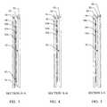
- FIG. 1is a composite of a monolithic structure with drive circuits on the edges outside the display area;
- FIG. 2is a cross section of the monolithic structure shown in FIG. 1 . with bottom emitting pixels and color filters under the pixel;
- FIG. 3is a cross section of the monolithic structure shown in FIG. 1 . with top emitting pixels and color filters coated on a top plate;
- FIG. 4is a cross section of the monolithic structure shown in FIG. 1 . with pattern coated top emitting pixels of different color;
- FIG. 5is a cross section of the monolithic structure shown in FIG. 1 . with pattern coated bottom-emitting pixels of different colors;
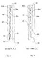
- FIG. 6is a composite of a monolithic structure including an island tile with TFT circuits and driver circuits under the display pixels;
- FIG. 7is a cross section of the monolithic structure shown in FIG. 6 with top emitting pixels and color filters coated on a top plate;
- FIG. 8is a cross section of the monolithic structure shown in FIG. 6 with pattern coated top emitting pixels of different colors;
- FIG. 9is a top view of a temporary coating support fixture
- FIG. 10is a front view of the coating support fixture shown in FIG. 9;
- FIG. 11is a side view of the coating support fixture shown in FIG. 9;
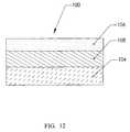
- FIG. 12is a cross section of a simple emissive pixel structure
- FIG. 13is a cross section of a top emitting pixel structure.
- FIGS. 1-5a composite view of a monolithic structure 20 is shown for an emissive display.
- the monolithic structure 20is composed of tiles 22 a-d that are preprocessed for edge quality.
- the tiles 22have thin film transistor (TFT) circuits 40 and bottom pixel electrode 104 or 304 arrays defining the active area of the display.
- TFTthin film transistor
- the drive electronics 34 and TFT 40 circuitsprovide electrical signals to pixels 100 in the corresponding tile. It is understood that the tiles 22 can be tested to ensure proper performance of the TFT circuits 40 and drive circuits 34 .
- the edges of the tiles 22are polished to maintain a parallel line to the bottom pixel electrode 104 or 304 array. Furthermore, the polishing reduces the distance from the outermost pixel to the tile 22 edge.
- the tiles 22are aligned with a position so that the pixel pitch 36 across the seam of the adjacent tiles is approximately equal to the pixel pitch 36 within the array of a single tile.
- the tiles 22can be affixed to each other using adhesive.
- higher temperature joining techniquescan be used to bond tiles to make the monolithic structure 20 .
- Light emitting materialsare sensitive to temperature and ultraviolet light; this severely limits the options for bonding tiles together.
- high temperature processesincluding metal bonding, high temperature adhesive, microwave bonding, and fusion joining can be used.
- ultraviolet adhesivescan be used prior to deposition of light emitting material 108 or 308 .
- the proximity of the pixel area to the space 32 between tilesprecludes the ability to mask only the pixel area; therefore, it would not be possible to use ultraviolet processes after deposition.
- the monolithic structure 20Prior to deposition of the light emitting material 108 or 308 the monolithic structure 20 can be thoroughly cleaned.
- Light emitting material 108 or 308is deposited onto the monolithic structure 20 . It is understood that the light emitting material 108 or 308 can be several materials that when layered or combined provide the desired light emitting properties when activated by an electric field. In addition, it is understood that the monolithic structure 20 can be supported by a carrier throughout processing. The material can be deposited in numerous ways including, but not limited to, evaporation, sublimation, and spin coating. The coatings 108 or 308 can be continuous across the monolithic structure 20 , extending beyond the edge of the tiles 22 and covering the space 32 between tiles 22 . When the coating is continuous the light emitting material 108 or 308 is monochromatic, with the preferred embodiment being white light emitting.
- the coatings 108 or 308include an electroluminescent material that produces light when activated by an electricfield.
- the top pixel electrode 106 or 306is subsequently deposited over the light emitting materials in the coatings 108 or 308 .
- the top pixel electrodes 106 or 306require a low work function conductive material.
- color filters 42 and a passivation layer 44can be formed on the tiles 22 prior to depositing the light transmissive bottom pixel electrode 104 .
- the color filters 42are aligned with bottom-emitting pixels 100 and can be patterned to provide a full color display; one color combination being red, green and blue.
- the multilayer organic top emitting pixels 300are top emitting and have a light transmissive top pixel electrode 306 a and b he color filters 42 , which are aligned to the multilayer organic top emitting pixels 300 , and the passivation layer 44 can be formed on a top plate 46 that serves as the viewing plane for the display.
- the color filters 42can be patterned to provide a full color display; one color combination being red, green and blue.
- the light emitting material 108is pattern deposited on the bottom pixel electrodes, 104 and viewed through the bottom.
- the depositioncan be accomplished by evaporation, sublimation, or other means.
- different pixels 100can emit different colored light including patterned color combinations that produce a full-color display.
- the light emitting material 308is pattern deposited on the bottom pixel electrode 304 and viewed through the top pixel electrode 306 .
- the monolithic structure 20can include island tiles 22 i.
- Island tiles 22 iare those tiles that do not have any drive circuits 34 at the perimeter of the monolithic structure 20 . All of the tiles 22 are mounted on a back plate 30 to form a monolithic structure 20 , which can then be coated.
- the island tiles 22 ican have vertical electrical connections to conductors on the back plate 30 .
- the TFT circuits 40 and the drive circuits 34can be moved under the bottom pixel electrodes 104 or 304 in order to allow pixels along all four edges of the island tile 22 i as disclosed in commonly assigned U.S. patent application Ser. No. 09/788,923 filed Feb. 20, 2001, entitled “Light-Producing High Aperture Display Having Aligned Tiles” by Henry R. Freidhoff et al., the disclosure of which is incorporated herein by reference.
- the tiles 22are properly aligned and then affixed to back plate 30 .
- the back plate 30becomes a permanent part of the monolithic structure 20 and provides support when operated as a final display.
- the space 32 between the tilescan be, but need not be, filled by adhesive or other means. Desiccant or an oxygen gettering material can also be placed in the space 32 .
- the tiles 22are affixed to the back plate 30 by adhesive, metal bonding, or other means.
- the back plate 30can be used to escape signal lines from the tiles 22 . Electrical connections can be made from the tiles 22 of the monolithic structure 20 to the back plate 30 . These connections can be made with conductive adhesive, flex, solder or other means. The connections can be made to vertical connections or run down the edges of the tile 22 .
- a temporary support fixture 50is used to temporarily secure tiles 22 for coating as a monolithic structure 20 wherein the temporary support fixture 50 is not a permanent support plate.
- the temporary support fixture 50provides protection of the polished edges of the tiles 22 .
- the tiles 22are later removed from the temporary support fixture 50 and realigned and mounted in the final assembly.
- the alignment and the spacing of the tiles 22 in the temporary support fixture 50are not critical during coating of the light emitting layer 108 or 308 and top pixel electrode 106 or 306 .
- the coatings 108 or 308 and 106 or 306can extend beyond the edge of the tiles to provide uniform coverage across all tiles.
- a polarization layer 48can be added to the viewing surface either the top plate 46 or back plate 30 to increase the contrast ratio of the display.
- the present inventionis applicable to emissive displays, and is particularly suitable for, but not limited to, use in organic electroluminescent, EL, displays.
- FIGS. 12 and 13show examples of pixels 100 and 300 with organic EL materials.
- a light-emitting layer of an organic EL tilecomprises a luminescent or fluorescent material where electroluminescence is produced as a result of electron-hole pair recombination in this region.
- the light-emitting layer 108is sandwiched between the bottom pixel electrode or 104 and top pixel electrode 106 .
- the light-emitting layeris a pure material with a high luminescent efficiency.
- a well-known materialis tris (8-quinolinato) aluminum, (Alq), which produces excellent green electroluminescence.
- the simple structure 100can be modified to a three-layer structure in which an additional EL layer is introduced between the hole and electron-transporting layers to function primarily as the site for hole-electron recombination and thus electroluminescence.
- the functions of the individual organic layersare distinct and can therefore be optimized independently.
- the electroluminescent or recombination layercan be chosen to have a desirable EL color as well as high luminance efficiency.
- the electron and hole transport layerscan be optimized primarily for the carrier transport property.
- the multilayer organic top emitting pixel 300when the top plate 46 is the viewing surface, the multilayer organic top emitting pixel 300 , as shown in FIG. 13, emits light from the top and has a substrate 302 on which is disposed a light reflective conductive bottom pixel layer 304 .
- the bottom pixel electrode 304comprises two layers 304 a and 304 b.
- 304 ais a light reflective conductive metal layer and 304 b is a thin light transmissive layer of a conductive high work function material.
- An organic light-emitting structure 308is formed between a top pixel electrode 306 and a bottom pixel electrode 304 .
- the top pixel electrode 306is composed of two layers 306 a and 306 b.
- 306 ais a thin light transmissive conductive layer of a low work function material and 306 b is a light transmissive conductive layer such as indium tin oxide.
- the organic light-emitting structure 308is comprised of, in sequence, an organic hole-transporting layer 310 , an organic light-emitting layer 312 , and an organic electron-transporting layer 314 .
- an electrical potential difference(not shown) is applied between the bottom pixel electrode 304 and the top pixel electrode 306 , the top pixel electrode 306 will inject electrons into the electron-transporting layer 314 , and the electrons will migrate across layer 314 to the light-emitting layer 312 .
- holeswill be injected from the bottom pixel electrode 304 into the hole-transporting layer 310 .
- the holeswill migrate across layer 310 and recombine with electrons at or near a junction formed between the hole-transporting layer 310 and the light-emitting layer 312 .
- a migrating electrondrops from its conduction band to a valence band in filling a hole, energy is released as light, and is emitted through the light-transmissive top pixel electrode 306 .
Landscapes
- Physics & Mathematics (AREA)
- Nonlinear Science (AREA)
- Mathematical Physics (AREA)
- Chemical & Material Sciences (AREA)
- Crystallography & Structural Chemistry (AREA)
- General Physics & Mathematics (AREA)
- Optics & Photonics (AREA)
- Devices For Indicating Variable Information By Combining Individual Elements (AREA)
- Electroluminescent Light Sources (AREA)
Abstract
Description
Claims (18)
Priority Applications (5)
| Application Number | Priority Date | Filing Date | Title |
|---|---|---|---|
| US09/815,076US6509941B2 (en) | 2001-03-22 | 2001-03-22 | Light-producing display having high aperture ratio pixels |
| TW091101659ATW588170B (en) | 2001-03-22 | 2002-01-31 | Method of making a tiled emissive display having at least two aligned tiles |
| JP2002034866AJP2002313569A (en) | 2001-03-22 | 2002-02-13 | Display of composing light with high aperture ratio pixel |
| EP02075943AEP1244146A3 (en) | 2001-03-22 | 2002-03-11 | A method of making a tiled emissive display |
| KR1020020015034AKR20020075261A (en) | 2001-03-22 | 2002-03-20 | Light-producing display having high aperture ratio pixels |
Applications Claiming Priority (1)
| Application Number | Priority Date | Filing Date | Title |
|---|---|---|---|
| US09/815,076US6509941B2 (en) | 2001-03-22 | 2001-03-22 | Light-producing display having high aperture ratio pixels |
Publications (2)
| Publication Number | Publication Date |
|---|---|
| US20020173215A1 US20020173215A1 (en) | 2002-11-21 |
| US6509941B2true US6509941B2 (en) | 2003-01-21 |
Family
ID=25216783
Family Applications (1)
| Application Number | Title | Priority Date | Filing Date |
|---|---|---|---|
| US09/815,076Expired - LifetimeUS6509941B2 (en) | 2001-03-22 | 2001-03-22 | Light-producing display having high aperture ratio pixels |
Country Status (5)
| Country | Link |
|---|---|
| US (1) | US6509941B2 (en) |
| EP (1) | EP1244146A3 (en) |
| JP (1) | JP2002313569A (en) |
| KR (1) | KR20020075261A (en) |
| TW (1) | TW588170B (en) |
Cited By (15)
| Publication number | Priority date | Publication date | Assignee | Title |
|---|---|---|---|---|
| US20030011724A1 (en)* | 2001-07-16 | 2003-01-16 | Sundahl Robert C. | Repairable tiled displays |
| US20030016227A1 (en)* | 2001-07-19 | 2003-01-23 | Matthies Dennis L. | Adaptable large area display |
| US20030218590A1 (en)* | 2002-05-23 | 2003-11-27 | Kiser David K. | Optics engine having multi-array spatial light modulating device and method of operation |
| US20040207315A1 (en)* | 2003-04-18 | 2004-10-21 | Thielemans Robbie | Organic light-emitting diode display assembly for use in a large-screen display application |
| US20040224435A1 (en)* | 2001-03-02 | 2004-11-11 | Fuji Photo Film Co., Ltd. | Method for producing organic thin film device and transfer material used therein |
| US20050042865A1 (en)* | 2003-08-19 | 2005-02-24 | International Business Machines Corporation | Atomic layer deposition of metallic contacts, gates and diffusion barriers |
| US20080061691A1 (en)* | 2005-05-12 | 2008-03-13 | Shinoda Plasma Co., Ltd. | Display device including gas discharge tubes |
| US20090073079A1 (en)* | 2007-09-19 | 2009-03-19 | Miller Michael E | Tiled passive matrix electro-luminescent display |
| US20120256556A1 (en)* | 2011-04-11 | 2012-10-11 | Sony Corporation | Light-emitting panel, display device and electronic equipment |
| WO2012145038A1 (en)* | 2011-04-19 | 2012-10-26 | Teledyne Rad-Icon Imaging Corp. | Method of direct silicon tiling of a tiled image sensor array |
| US10741107B2 (en) | 2013-12-31 | 2020-08-11 | Ultravision Technologies, Llc | Modular display panel |
| US10891881B2 (en) | 2012-07-30 | 2021-01-12 | Ultravision Technologies, Llc | Lighting assembly with LEDs and optical elements |
| US20220018015A1 (en)* | 2008-01-04 | 2022-01-20 | Nanolumens Acquisition, Inc. | Display Apparatus and Methods |
| US11374053B2 (en) | 2017-11-08 | 2022-06-28 | Corning Incorporated | Apparatus and methods for assembling a display area |
| US11425826B2 (en) | 2017-07-11 | 2022-08-23 | Corning Incorporated | Tiled displays and methods of manufacturing the same |
Families Citing this family (16)
| Publication number | Priority date | Publication date | Assignee | Title |
|---|---|---|---|---|
| KR100720425B1 (en)* | 2002-12-24 | 2007-05-22 | 엘지.필립스 엘시디 주식회사 | LCD Display |
| JP4059153B2 (en) | 2003-06-23 | 2008-03-12 | ソニー株式会社 | Manufacturing method of display device |
| US7011987B2 (en)* | 2003-07-01 | 2006-03-14 | Ritdisplay Corporation | Method of fabricating organic electroluminescence panel package |
| JP2005302440A (en)* | 2004-04-08 | 2005-10-27 | Mitsubishi Electric Corp | Organic electroluminescence display |
| US7262438B2 (en) | 2005-03-08 | 2007-08-28 | Avago Technologies Ecbu Ip (Singapore) Pte. Ltd. | LED mounting having increased heat dissipation |
| DE102008005497A1 (en)* | 2008-01-22 | 2009-07-23 | Osram Opto Semiconductors Gmbh | Optoelectronic component and method for producing an optoelectronic component and a wafer |
| CN103797531A (en)* | 2012-09-10 | 2014-05-14 | 深圳市柔宇科技有限公司 | Large-size display screen and manufacturing method therefor |
| WO2014043850A1 (en)* | 2012-09-18 | 2014-03-27 | 深圳市柔宇科技有限公司 | Large-size display screen and manufacturing method thereof |
| CN105336762B (en)* | 2015-11-17 | 2019-01-11 | 深圳典邦科技有限公司 | The OLED image display device and manufacturing method of silicon base CMOS driving |
| US10079264B2 (en)* | 2015-12-21 | 2018-09-18 | Hong Kong Beida Jade Bird Display Limited | Semiconductor devices with integrated thin-film transistor circuitry |
| CN107967895A (en)* | 2017-12-22 | 2018-04-27 | 重庆秉为科技有限公司 | A kind of OLED arrays passive drive circuit |
| WO2020188542A1 (en)* | 2019-03-20 | 2020-09-24 | Vuereal Inc. | Tiled display for optoelectronic system |
| CN111081158A (en)* | 2019-12-30 | 2020-04-28 | 深圳市华星光电半导体显示技术有限公司 | Spliced display screen, preparation method thereof and display device |
| CN113934030B (en) | 2020-06-29 | 2023-01-24 | 京东方科技集团股份有限公司 | Display panel, manufacturing method thereof, and display device |
| KR20220049082A (en) | 2020-10-13 | 2022-04-21 | 삼성디스플레이 주식회사 | Tiling display, Display panel alignment device and Manufacturing method for the same |
| KR20230027391A (en)* | 2021-08-18 | 2023-02-28 | 삼성디스플레이 주식회사 | Tiled display device |
Citations (7)
| Publication number | Priority date | Publication date | Assignee | Title |
|---|---|---|---|---|
| US5179459A (en)* | 1991-06-28 | 1993-01-12 | Compag Computer Corporation | Methods for adhering multiple stack liquid crystal display panels |
| US5781258A (en) | 1996-06-13 | 1998-07-14 | Rainbow Displays, Inc. | Assembling and sealing large, hermetic and semi-hermetic, h-tiled, flat-paneled displays |
| US5889568A (en) | 1995-12-12 | 1999-03-30 | Rainbow Displays Inc. | Tiled flat panel displays |
| US5903328A (en) | 1997-06-16 | 1999-05-11 | Rainbow Displays, Inc. | Tiled flat-panel display with tile edges cut at an angle and tiles vertically shifted |
| US6133969A (en)* | 1999-05-28 | 2000-10-17 | Rainbow Displays, Inc. | Maintaining three-dimensional tolerances while manufacturing AMLCD displays |
| US6184952B1 (en)* | 1999-09-15 | 2001-02-06 | Rainbow Displays, Inc. | Compensation for edge effects and cell gap variation in tiled flat-panel, liquid crystal displays |
| US6259497B1 (en)* | 1991-03-28 | 2001-07-10 | The Secretary Of State For Defence In Her Brittanic Majesty's Government Of The United Kingdom Of Great Britain And Northern Ireland | Large area liquid crystal displays |
Family Cites Families (6)
| Publication number | Priority date | Publication date | Assignee | Title |
|---|---|---|---|---|
| JPH10268332A (en)* | 1997-03-24 | 1998-10-09 | Sharp Corp | Liquid crystal display device and method of manufacturing the same |
| JP3498895B2 (en)* | 1997-09-25 | 2004-02-23 | シャープ株式会社 | Substrate cutting method and display panel manufacturing method |
| US6370019B1 (en)* | 1998-02-17 | 2002-04-09 | Sarnoff Corporation | Sealing of large area display structures |
| US8853696B1 (en)* | 1999-06-04 | 2014-10-07 | Semiconductor Energy Laboratory Co., Ltd. | Electro-optical device and electronic device |
| TW522453B (en)* | 1999-09-17 | 2003-03-01 | Semiconductor Energy Lab | Display device |
| JP3676142B2 (en)* | 1999-09-29 | 2005-07-27 | 三洋電機株式会社 | Method for manufacturing electroluminescence display device |
- 2001
- 2001-03-22USUS09/815,076patent/US6509941B2/ennot_activeExpired - Lifetime
- 2002
- 2002-01-31TWTW091101659Apatent/TW588170B/ennot_activeIP Right Cessation
- 2002-02-13JPJP2002034866Apatent/JP2002313569A/ennot_activeWithdrawn
- 2002-03-11EPEP02075943Apatent/EP1244146A3/ennot_activeWithdrawn
- 2002-03-20KRKR1020020015034Apatent/KR20020075261A/ennot_activeCeased
Patent Citations (7)
| Publication number | Priority date | Publication date | Assignee | Title |
|---|---|---|---|---|
| US6259497B1 (en)* | 1991-03-28 | 2001-07-10 | The Secretary Of State For Defence In Her Brittanic Majesty's Government Of The United Kingdom Of Great Britain And Northern Ireland | Large area liquid crystal displays |
| US5179459A (en)* | 1991-06-28 | 1993-01-12 | Compag Computer Corporation | Methods for adhering multiple stack liquid crystal display panels |
| US5889568A (en) | 1995-12-12 | 1999-03-30 | Rainbow Displays Inc. | Tiled flat panel displays |
| US5781258A (en) | 1996-06-13 | 1998-07-14 | Rainbow Displays, Inc. | Assembling and sealing large, hermetic and semi-hermetic, h-tiled, flat-paneled displays |
| US5903328A (en) | 1997-06-16 | 1999-05-11 | Rainbow Displays, Inc. | Tiled flat-panel display with tile edges cut at an angle and tiles vertically shifted |
| US6133969A (en)* | 1999-05-28 | 2000-10-17 | Rainbow Displays, Inc. | Maintaining three-dimensional tolerances while manufacturing AMLCD displays |
| US6184952B1 (en)* | 1999-09-15 | 2001-02-06 | Rainbow Displays, Inc. | Compensation for edge effects and cell gap variation in tiled flat-panel, liquid crystal displays |
Non-Patent Citations (1)
| Title |
|---|
| US 5,980,348, 11/1999, Gaynes et al. (withdrawn) |
Cited By (21)
| Publication number | Priority date | Publication date | Assignee | Title |
|---|---|---|---|---|
| US20040224435A1 (en)* | 2001-03-02 | 2004-11-11 | Fuji Photo Film Co., Ltd. | Method for producing organic thin film device and transfer material used therein |
| US7075106B2 (en)* | 2001-03-02 | 2006-07-11 | Fuji Photo Film Co. Ltd. | Method for producing organic thin film device and transfer material used therein |
| US20030011724A1 (en)* | 2001-07-16 | 2003-01-16 | Sundahl Robert C. | Repairable tiled displays |
| US20030016227A1 (en)* | 2001-07-19 | 2003-01-23 | Matthies Dennis L. | Adaptable large area display |
| US20030218590A1 (en)* | 2002-05-23 | 2003-11-27 | Kiser David K. | Optics engine having multi-array spatial light modulating device and method of operation |
| US20040207315A1 (en)* | 2003-04-18 | 2004-10-21 | Thielemans Robbie | Organic light-emitting diode display assembly for use in a large-screen display application |
| US20050042865A1 (en)* | 2003-08-19 | 2005-02-24 | International Business Machines Corporation | Atomic layer deposition of metallic contacts, gates and diffusion barriers |
| US7880374B2 (en)* | 2005-05-12 | 2011-02-01 | Shinoda Plasma Co., Ltd. | Display device including gas discharge tubes sandwiched between a front support member and rear support members |
| US20080061691A1 (en)* | 2005-05-12 | 2008-03-13 | Shinoda Plasma Co., Ltd. | Display device including gas discharge tubes |
| US7995002B2 (en) | 2007-09-19 | 2011-08-09 | Global Oled Technology Llc | Tiled passive matrix electro-luminescent display |
| US20090073079A1 (en)* | 2007-09-19 | 2009-03-19 | Miller Michael E | Tiled passive matrix electro-luminescent display |
| US20220018015A1 (en)* | 2008-01-04 | 2022-01-20 | Nanolumens Acquisition, Inc. | Display Apparatus and Methods |
| US20120256556A1 (en)* | 2011-04-11 | 2012-10-11 | Sony Corporation | Light-emitting panel, display device and electronic equipment |
| US8742675B2 (en)* | 2011-04-11 | 2014-06-03 | Sony Corporation | Light-emitting panel, display device and electronic equipment |
| WO2012145038A1 (en)* | 2011-04-19 | 2012-10-26 | Teledyne Rad-Icon Imaging Corp. | Method of direct silicon tiling of a tiled image sensor array |
| US10891881B2 (en) | 2012-07-30 | 2021-01-12 | Ultravision Technologies, Llc | Lighting assembly with LEDs and optical elements |
| US10741107B2 (en) | 2013-12-31 | 2020-08-11 | Ultravision Technologies, Llc | Modular display panel |
| US11425826B2 (en) | 2017-07-11 | 2022-08-23 | Corning Incorporated | Tiled displays and methods of manufacturing the same |
| US11374053B2 (en) | 2017-11-08 | 2022-06-28 | Corning Incorporated | Apparatus and methods for assembling a display area |
| US11881501B2 (en) | 2017-11-08 | 2024-01-23 | Corning Incorporated | Apparatus and methods for assembling a display area |
| US12100729B2 (en) | 2017-11-08 | 2024-09-24 | Corning Incorporated | Apparatus and methods for assembling a display area |
Also Published As
| Publication number | Publication date |
|---|---|
| JP2002313569A (en) | 2002-10-25 |
| TW588170B (en) | 2004-05-21 |
| KR20020075261A (en) | 2002-10-04 |
| US20020173215A1 (en) | 2002-11-21 |
| EP1244146A3 (en) | 2007-01-17 |
| EP1244146A2 (en) | 2002-09-25 |
Similar Documents
| Publication | Publication Date | Title |
|---|---|---|
| US6509941B2 (en) | Light-producing display having high aperture ratio pixels | |
| US6853411B2 (en) | Light-producing high aperture ratio display having aligned tiles | |
| US6624570B1 (en) | Electroluminescent display device and method for its fabrication | |
| KR100656324B1 (en) | Display device | |
| USRE41603E1 (en) | Tiled electronic display structure and method for modular repair thereof | |
| US7187118B2 (en) | Dual panel type organic electro luminescent display device and manufacturing method for the same | |
| KR101695082B1 (en) | Display device | |
| US6580214B2 (en) | Color display apparatus having electroluminescence elements | |
| JP3961981B2 (en) | Organic electroluminescent device and manufacturing method thereof | |
| KR101539874B1 (en) | Substrate to which film is formed and organic el display device | |
| CN103682146B (en) | White-light luminescent component including this white luminous panel and its manufacture method | |
| TWI699882B (en) | Electro-optical device and electronic apparatus | |
| KR20180046568A (en) | Display device having a white emitting area | |
| US20070018156A1 (en) | Dual panel type organic electroluminescent device | |
| KR102407887B1 (en) | Organic light emitting diode display apparatus and manufacturing method of the same | |
| CN102034848A (en) | Organic EL panel and panel junction type light emitting device | |
| JP4378798B2 (en) | Flat display element | |
| US7459848B2 (en) | Organic electroluminescence device and fabrication method thereof | |
| KR100353904B1 (en) | Organic electroluminescent display device and method of manufacturing the same | |
| JP2008076987A (en) | Organic EL display panel and manufacturing method thereof | |
| JP2008157986A (en) | Manufacturing method of organic EL display and organic EL display manufactured by the manufacturing method | |
| KR101694408B1 (en) | Organic electroluminescent device and Method of fabricating the same | |
| US6617785B2 (en) | Electroluminescence display unit and method of fabricating the same | |
| KR100623450B1 (en) | Organic electroluminescent display device and manufacturing method thereof | |
| KR101392202B1 (en) | organic electroluminescent device |
Legal Events
| Date | Code | Title | Description |
|---|---|---|---|
| AS | Assignment | Owner name:EASTMAN KODAK COMPANY, NEW YORK Free format text:ASSIGNMENT OF ASSIGNORS INTEREST;ASSIGNORS:FREIDHOFF, HENRY R.;PHELAN, GIANA M.;REEL/FRAME:011639/0675;SIGNING DATES FROM 20010227 TO 20010319 | |
| FEPP | Fee payment procedure | Free format text:PAYOR NUMBER ASSIGNED (ORIGINAL EVENT CODE: ASPN); ENTITY STATUS OF PATENT OWNER: LARGE ENTITY | |
| STCF | Information on status: patent grant | Free format text:PATENTED CASE | |
| FPAY | Fee payment | Year of fee payment:4 | |
| FEPP | Fee payment procedure | Free format text:PAYER NUMBER DE-ASSIGNED (ORIGINAL EVENT CODE: RMPN); ENTITY STATUS OF PATENT OWNER: LARGE ENTITY Free format text:PAYOR NUMBER ASSIGNED (ORIGINAL EVENT CODE: ASPN); ENTITY STATUS OF PATENT OWNER: LARGE ENTITY | |
| AS | Assignment | Owner name:GLOBAL OLED TECHNOLOGY LLC,DELAWARE Free format text:ASSIGNMENT OF ASSIGNORS INTEREST;ASSIGNOR:EASTMAN KODAK COMPANY;REEL/FRAME:023998/0368 Effective date:20100122 Owner name:GLOBAL OLED TECHNOLOGY LLC, DELAWARE Free format text:ASSIGNMENT OF ASSIGNORS INTEREST;ASSIGNOR:EASTMAN KODAK COMPANY;REEL/FRAME:023998/0368 Effective date:20100122 | |
| FPAY | Fee payment | Year of fee payment:8 | |
| FPAY | Fee payment | Year of fee payment:12 |