US6509722B2 - Dynamic input stage biasing for low quiescent current amplifiers - Google Patents
Dynamic input stage biasing for low quiescent current amplifiersDownload PDFInfo
- Publication number
- US6509722B2 US6509722B2US09/846,844US84684401AUS6509722B2US 6509722 B2US6509722 B2US 6509722B2US 84684401 AUS84684401 AUS 84684401AUS 6509722 B2US6509722 B2US 6509722B2
- Authority
- US
- United States
- Prior art keywords
- input
- amplifier
- output
- control signal
- stage
- Prior art date
- Legal status (The legal status is an assumption and is not a legal conclusion. Google has not performed a legal analysis and makes no representation as to the accuracy of the status listed.)
- Expired - Lifetime
Links
- 230000004044responseEffects0.000claimsabstractdescription32
- 230000001276controlling effectEffects0.000claimsdescription27
- 230000001105regulatory effectEffects0.000claimsdescription17
- 238000000034methodMethods0.000claimsdescription8
- 230000011664signalingEffects0.000claims2
- 230000003071parasitic effectEffects0.000abstractdescription5
- 230000001419dependent effectEffects0.000description5
- 238000010586diagramMethods0.000description5
- 239000003990capacitorSubstances0.000description4
- 239000004065semiconductorSubstances0.000description4
- 230000007423decreaseEffects0.000description3
- 238000013461designMethods0.000description3
- 230000008901benefitEffects0.000description2
- 238000012986modificationMethods0.000description2
- 230000004048modificationEffects0.000description2
- XUIMIQQOPSSXEZ-UHFFFAOYSA-NSiliconChemical compound[Si]XUIMIQQOPSSXEZ-UHFFFAOYSA-N0.000description1
- 238000013459approachMethods0.000description1
- 230000033228biological regulationEffects0.000description1
- 230000001413cellular effectEffects0.000description1
- 238000004519manufacturing processMethods0.000description1
- 238000012544monitoring processMethods0.000description1
- 230000000737periodic effectEffects0.000description1
- 230000008569processEffects0.000description1
- 229910052710siliconInorganic materials0.000description1
- 239000010703siliconSubstances0.000description1
- 238000004513sizingMethods0.000description1
Images


Classifications
- H—ELECTRICITY
- H03—ELECTRONIC CIRCUITRY
- H03F—AMPLIFIERS
- H03F3/00—Amplifiers with only discharge tubes or only semiconductor devices as amplifying elements
- H03F3/45—Differential amplifiers
- H03F3/45071—Differential amplifiers with semiconductor devices only
- H03F3/45076—Differential amplifiers with semiconductor devices only characterised by the way of implementation of the active amplifying circuit in the differential amplifier
- H03F3/45179—Differential amplifiers with semiconductor devices only characterised by the way of implementation of the active amplifying circuit in the differential amplifier using MOSFET transistors as the active amplifying circuit
- H03F3/45183—Long tailed pairs
- G—PHYSICS
- G05—CONTROLLING; REGULATING
- G05F—SYSTEMS FOR REGULATING ELECTRIC OR MAGNETIC VARIABLES
- G05F1/00—Automatic systems in which deviations of an electric quantity from one or more predetermined values are detected at the output of the system and fed back to a device within the system to restore the detected quantity to its predetermined value or values, i.e. retroactive systems
- G05F1/10—Regulating voltage or current
- G05F1/46—Regulating voltage or current wherein the variable actually regulated by the final control device is DC
- G05F1/56—Regulating voltage or current wherein the variable actually regulated by the final control device is DC using semiconductor devices in series with the load as final control devices
- G05F1/565—Regulating voltage or current wherein the variable actually regulated by the final control device is DC using semiconductor devices in series with the load as final control devices sensing a condition of the system or its load in addition to means responsive to deviations in the output of the system, e.g. current, voltage, power factor
- H—ELECTRICITY
- H03—ELECTRONIC CIRCUITRY
- H03F—AMPLIFIERS
- H03F2203/00—Indexing scheme relating to amplifiers with only discharge tubes or only semiconductor devices as amplifying elements covered by H03F3/00
- H03F2203/45—Indexing scheme relating to differential amplifiers
- H03F2203/45454—Indexing scheme relating to differential amplifiers the CSC comprising biasing means controlled by the input signal
- H—ELECTRICITY
- H03—ELECTRONIC CIRCUITRY
- H03F—AMPLIFIERS
- H03F2203/00—Indexing scheme relating to amplifiers with only discharge tubes or only semiconductor devices as amplifying elements covered by H03F3/00
- H03F2203/45—Indexing scheme relating to differential amplifiers
- H03F2203/45462—Indexing scheme relating to differential amplifiers the CSC comprising a cascode circuit
- H—ELECTRICITY
- H03—ELECTRONIC CIRCUITRY
- H03F—AMPLIFIERS
- H03F2203/00—Indexing scheme relating to amplifiers with only discharge tubes or only semiconductor devices as amplifying elements covered by H03F3/00
- H03F2203/45—Indexing scheme relating to differential amplifiers
- H03F2203/45466—Indexing scheme relating to differential amplifiers the CSC being controlled, e.g. by a signal derived from a non specified place in the dif amp circuit
Definitions
- the present inventionrelates generally to amplifier circuits for use in regulator circuits and other applications, and more particularly relates to amplifiers having dynamic input stage biasing for minimized quiescent current operation.
- Regulator circuitsare well known for providing a specified and constant output voltage or current from a poorly defined and often fluctuating input voltage or current.
- the regulation and control of supply voltage, particularly under changing load conditions,is perhaps one of the most fundamental and critical requirements of any electronic system design. For this reason, monolithic voltage regulator or power control circuits are considered to be among the essential building blocks of any analog or digital system.
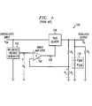
- FIG. 1illustrates a simplified block diagram depicting a conventional linear series regulator circuit 100 .
- the basic series regulatoris a feedback circuit comprised of three primary sub-circuits, namely, a reference voltage generator 102 , an error amplifier 104 and a pass element 106 .
- the reference voltage generator 102generates a reference voltage V R that is substantially independent of both the unregulated supply voltage V IN to which the reference voltage generator is connected, and temperature variations.
- the error amplifier 104compares the reference voltage V R with a measured voltage V S which represents a scaled version of a regulated output voltage V O of the regulator.
- This scaled voltage V Sis typically derived from a simple tapped resistive divider, for example comprised of resistors R 1 and R 2 connected in series across the output V O .
- Error amplifier 104generates an error output signal at node 108 which is coupled to the pass element 106 for regulating a voltage drop across the pass element 106 such that the scaled voltage V S is held substantially equal to the reference voltage V R .
- a more detailed discussion of regulator circuit fundamentalsis presented, for example, in the text A. B. Grebene, Bipolar and MOS Analog Integrated Circuit Design , John Wiley & Sons, pp. 481-514 (1984), which is incorporated herein by reference.
- a high-current p-channel metal-oxide-semiconductor (PMOS) transistor device(not shown) is employed as the series-pass element 106 .
- the gate terminal of the PMOS devicein this instance, is coupled to the output of the error amplifier, the source terminal of the PMOS device is coupled to the unregulated input V IN and the drain terminal of the PMOS device forms the regulated output node V O .
- the resistance of the PMOS device, and hence the voltage drop across the device,is controlled by the error output signal generated by the error amplifier 104 to regulate the output voltage V O as stated above.
- the loop bandwidth of a feedback circuitis primarily dominated by a large external capacitance C BYP . (and equivalent series resistance R ESR ), which is typically on the order of one microfarad (1 ⁇ F), and an effective output resistance R O of the regulator.
- C BYPand equivalent series resistance R ESR
- R Oeffective output resistance
- the combination of C BYP and R Oresults in a pole being formed which creates a 3-dB rolloff in the range of several hertz or less.
- the resulting rapid rolloff of gain at higher frequenciescan significantly degrade certain performance characteristics of the regulator, such as, for example, ripple rejection (which is a measure of the regulator's ability to reject periodic fluctuations of rectified ac voltage signals at the input of the regulator).
- VCOsvoltage-controlled oscillators
- RFradio frequency
- the present inventionprovides an amplifier, for use in regulator circuits and other applications, which dissipates a minimized quiescent current at low output current operation while providing enhanced stability and dynamic response across a wide range of load currents and load capacitance values.
- the inventionemploys a dynamic input stage biasing architecture, whereby input stage bias current is operatively controlled as a function of output load current, thereby increasing the bandwidth of the amplifier as load current increases. In this manner, parasitic poles associated with the amplifier are pushed out in frequency so as not to compromise amplifier stability, particularly at low output load current levels, as the dominant pole formed by the amplifier output impedance and output bypass capacitance increases with increased load current.
- an amplifier having dynamic input stage biasingincludes an input stage operatively coupled to an input of the amplifier.
- a controlled current sourceis coupled to the input stage and is responsive to a control signal for at least partially controlling an input bias current generated by the controlled current source.
- the amplifierfurther includes a sense circuit which is operatively connected in a feedback arrangement between an output of the amplifier and the controlled current source. The sense circuit measures an output load current from the amplifier and generates the control signal in response thereto. In this manner, the input bias current, as well as the amplifier bandwidth, is a function of the output load current of the amplifier.
- FIG. 1is a schematic diagram illustrating a conventional series regulator circuit.
- FIG. 2is a schematic diagram depicting an illustrative regulator circuit, formed in accordance with the present invention.
- FIG. 3is a schematic diagram depicting details of the error amplifier of the illustrative regulator circuit shown in FIG. 2, formed in accordance with the present invention.
- FIGS. 4A and 4Bare schematic diagrams depicting an exemplary linear regulator circuit implementation, formed in accordance with the present invention.
- CMOScomplimentary metal-oxide-semiconductor
- BJTbipolar junction transistor
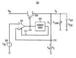
- FIG. 2depicts a series regulator circuit 200 employing dynamic input stage biasing in accordance with one aspect of the invention.
- the illustrative regulator circuit 200includes an error amplifier 202 , a current sense circuit 204 , and a pass element implemented as a PMOS transistor device 206 .
- the pass transistor 206is connected so that its source terminal (S) is coupled to the unregulated input V IN and the drain terminal (D) forms a regulated output V O of the regulator circuit 200 .
- a tapped voltage dividerfor example comprised of two or more resistors R 1 and R 2 connected in a series configuration, is coupled between the drain terminal of the pass transistor 206 and circuit ground and may be used for providing a current sink path for transistor 206 (e.g., as a load or pull-down) in addition to measuring a predetermined portion of the output V O .
- the voltage dividermay be implemented using one or more active devices (e.g., a transistor biased to an appropriate quiescent point), either in place of or in addition to the one or more resistors in the voltage divider, as will be understood by those skilled in the art.
- the external regulator loadmay be represented as a load resistor R LOAD and a load capacitor C BYP (having an equivalent series resistance R ESR associated therewith) coupled together in parallel across the output V O of the regulator circuit.
- the load resistor R LOADis depicted as a variable resistance element to represent the wide range of output load current which the regulator circuit may be required to supply.
- the error amplifier 202is preferably a differential amplifier, such as, for example, an operational amplifier, having a non-inverting or positive input (+), an inverting or negative input ( ⁇ ) and an output coupled to a gate terminal (G) of the pass transistor 206 at node 214 .
- the error amplifier 202preferably compares a measured voltage V M (e.g., developed across resistor R 2 of the voltage divider), coupled to the inverting input of the error amplifier at node 210 with a reference voltage V REF (e.g., generated by a voltage source 208 which is ideally independent of the unregulated supply), coupled to the non-inverting input of the error amplifier, and generates a corrective error signal at the output of the error amplifier.
- V Me.g., developed across resistor R 2 of the voltage divider
- V REFe.g., generated by a voltage source 208 which is ideally independent of the unregulated supply
- An effective impedance, and hence voltage drop, of the pass device 206is modulated by the corrective error signal from the error amplifier 202 such that the output V O of the regulator circuit is held at a substantially constant predefined voltage, regardless of the input voltage V IN .
- the measured voltage V Mis derived from the regulated output V O by means of a resistive divider comprising series-connected resistors R 1 and R 2 , as explained above. In this manner, a feedback loop is established around the error amplifier.
- the input connections to the error amplifier 202may be reversed, in which case the polarity type of the pass transistor 206 could likewise be reversed (e.g., NMOS device) and the transistor would be used in a follower arrangement thereby avoiding a positive feedback condition, as will be understood by those skilled in the art.
- the polarity type of the pass transistor 206could likewise be reversed (e.g., NMOS device) and the transistor would be used in a follower arrangement thereby avoiding a positive feedback condition, as will be understood by those skilled in the art.
- the error amplifier 202further includes at least one bias control input for receiving at least one control signal, e.g., via line 212 , and operatively controlling an input bias current of the error amplifier in response thereto. Details of an illustrative error amplifier formed in accordance with the invention will be described below in conjunction with FIGS. 3 and 4.
- the current sense circuit 204is operatively coupled to the output 214 of the error amplifier 202 .
- the current sense circuit 204monitors an output voltage or current produced by the error amplifier 202 and generates the control signal on line 212 in response thereto.
- the control signal generated by the current sense circuit 204is preferably fed back to the bias control input of the error amplifier 202 for dynamically controlling an input stage bias current in the error amplifier, preferably in proportion to the sensed output voltage or current produced by the error amplifier.
- Control signal 212may be in the form of a predetermined portion of output current generated by the error amplifier. In this instance, as the output load current from the error amplifier 202 increases, the amount of current being fed back to the error amplifier increases proportionally.
- control signal 212 from the current sense circuit 204can be summed with a current produced by a bias generator (not shown) in the error amplifier 202 so as to generate an input bias current for the input stage of the error amplifier that is a function of the output load current from the regulator circuit.
- a bias generatornot shown
- This novel input stage biasing architectureprovides superior stability, particularly at low output load current levels.
- other suitable voltage-dependent or current-dependent current source architecturesmay be similarly employed with the present invention in accordance with the principles set forth herein.
- the effective bandwidth of the regulator circuit 200increases with increasing output load current, due, to a large extent, to an increase in small signal transconductance characteristics (e.g., g m and g o ) associated with transistor devices comprising the error amplifier 202 . Consequently, since the parasitic capacitances of the transistor devices increase with increasing load current, and since the value of load capacitance remains essentially constant, the parasitic poles of the error amplifier become significantly more influential in determining an overall loop stability of the regulator circuit. Additionally, since the output impedance of the regulator circuit decreases with increasing output load current, the pole formed by the output capacitance and the output impedance of the regulator is pushed farther out in frequency. Hence, this pole can no longer be considered a dominant pole compared to other parasitic poles in the regulator circuit.
- small signal transconductance characteristicse.g., g m and g o
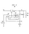
- the error amplifier 202 in this embodimentis implemented as a differential amplifier (e.g., an operational amplifier or suitable alternative thereof) including a first or input differential stage comprised of two NMOS transistor devices 304 and 306 , each device having a gate (G), a source (S) and a drain (D) terminal.
- the two transistor devices 304 , 306are coupled together in a differential pair configuration, with a common source or tail connection at node 312 .
- the gate terminals of the transistor devices 304 , 306form non-inverting and inverting inputs, respectively, of the error amplifier 202 .
- each input transistor device 304 , 306are coupled to a corresponding input load 308 .
- the input load 308maybe implemented, for example, as a pair of resistors of substantially equal value, each resistor being connected at a first end to the drain terminal of a corresponding one of the input devices 304 , 306 , and to a positive voltage supply (e.g., V IN ) at a second end.
- the input load 308maybe implemented, for example, using a pair of active devices (e.g., transistors) biased to an appropriate quiescent operating point.
- An output 316 of the input stage of the error amplifieris formed in this embodiment at a junction between the drain terminal of transistor device 306 and a corresponding terminal of input load 308 .
- the input stage of the error amplifier 202further includes a controlled current source 302 operatively coupled to the tail node 312 for supplying a bias current I BIAS to the input stage.
- the controlled current source 302is responsive to a control signal (e.g., a control voltage or current) for selectively controlling the bias current I BIAS flowing through the input stage.
- Controlled current sources suitable for use with the present inventioninclude voltage-controlled current sources (VCCS) and current-controlled current sources (CCCS), e.g., current differential amplifiers.
- VCCSvoltage-controlled current sources
- CCCScurrent-controlled current sources
- a more detailed discussion of such controlled current sourcesmay be found, for example, in the text by P. E. Allen and D. R. Holberg, CMOS Analog Circuit Design , Holt, Rinehart & Winston, pp. 308-313 (1987), which is incorporated herein by reference.
- the error amplifier 202 in this embodimentfurther comprises a second stage 310 coupled to the output 316 of the input stage.
- This second stage 310may be an output stage, assuming no subsequent amplifier stages are used (as shown in FIG. 3 ).
- the second stage 310may be employed where it is advantageous to isolate the input stage of the error amplifier 202 from such external conditions or a subsequent amplifier stage.
- the second stage 310may, for instance, provide sufficient output power in the form of voltage or current.
- the second stage 310may be configured to provide a predetermined gain, or it may provide unity gain consistent with a standard buffer circuit.
- the second stage 310may also include level shifting circuitry for setting an output voltage of the error amplifier to a predetermined value, as necessary.
- An output of the second stage 310if such a stage is employed, forms the overall output 214 of the error amplifier 202 for modulating the impedance of the pass transistor 206 , as explained above.
- the reference voltage source 208which, as previously stated, generates a substantially constant voltage V REF (e.g., supply-independent and temperature-independent), is operatively coupled to the non-inverting input of the error amplifier 202 .
- the inverting input of the error amplifieris operatively coupled to the measured voltage V M , at node 210 , corresponding to a predetermined portion of the output voltage V O of the regulator circuit 300 .
- the feedback circuitcomprising the error amplifier 202 and the pass transistor 206 holds the measured voltage V M substantially equal to the reference voltage V REF . Therefore, using the above equation, the resistors R 1 and R 2 can be selected to produce a desired regulated output voltage V O and/or quiescent pull-down current flowing through the resistor divider.
- the illustrative regulator circuit 300further comprises current sense circuit 204 coupled to the output 214 of the error amplifier 202 for operatively monitoring a representative output (e.g., output load current) of the regulator circuit and generating the control signal 212 in response thereto.
- the control signal 212is coupled to the controlled current source 302 in the error amplifier 202 and preferably provides a path for feeding back at least a portion of the output voltage or current supplied by the pass transistor 206 to dynamically control the bias current of the input stage of the error amplifier, as explained above in conjunction with FIG. 2 .
- a load-dependent (dynamic) bias feedback architecturemay be implemented in other functional sub-circuits of the regulator circuit 300 in addition to and consistent with the dynamic input stage biasing described herein.
- the control signal on line 212(or other signal which is a function of the regulator output) from the current sense circuit 204 may also be coupled to the input stage load 308 and/or the second stage 310 of the error amplifier 202 .
- Each of these additional load-dependent bias current feedback pathsmay be similarly used to dynamically control one or more characteristics of the respective circuits to which such feedback path is coupled.
- the second stage 3may include a controlled current source (not shown) consistent with the controlled current source 302 included in the input stage of the error amplifier.
- control signalmay be used to dynamically increase a quiescent current in the second stage 310 when an increase in output load current is detected, or vice versa.
- the benefits of dynamic input stage biasingcan be similarly applied to other functional sub-circuits in the regulator circuit 300 .
- FIG. 4Athere is shown an exemplary linear regulator circuit formed in accordance with an illustrative embodiment of the invention.
- the exemplary regulator circuit 400incorporates the dynamic input biasing architecture of the present invention.
- the regulator circuit 400includes an error amplifier 402 , details of which are shown in FIG. 4B, having an output 414 coupled to the gate (G) terminal of a PMOS transistor device 408 functioning as a pass element.
- An output voltage OUTAis developed at the output 414 .
- the source (S) terminal of the pass transistor 408is coupled to the unregulated input V IN of the regulator circuit 400 and the drain (D) terminal of transistor 408 forms a regulated output V O of the regulator circuit, in a manner similar to that previously explained in connection with FIG. 2 .
- Voltage source 208is coupled to an input of the error amplifier 402 (e.g., inverting input INN) and as previously noted supplies a reference voltage V REF that is ideally independent of supply voltage and temperature variations.
- the voltage reference 208may be generated internal to the regulator 400 , such as with a bandgap reference circuit. Similarly, such reference voltage V REF may be supplied from an external voltage source.
- the input connections to the error amplifier 402may be reversed, in which case the polarity type of pass transistor 408 could likewise be reversed (e.g., NMOS device) and transistor 408 would be used in a follower configuration to avoid a positive feedback condition, as will be understood by those skilled in the art.
- the error amplifier 402compares the reference voltage V REF with the measured voltage V M coupled to a second input of the error amplifier (e.g., non-inverting input INP), which as previously noted represents at least a portion of the regulator circuit output V O , at node 4 and generates an error signal at the output 414 of the error amplifier in response to a difference between the two voltages V REF and V M .
- the measured voltage V Mmay be derived from the regulator circuit output V O by means of a tapped voltage divider circuit, or a suitable alternative thereof.
- the voltage divider circuitpreferably comprises two resistors R 1 and R 2 connected together in series across the regulated output V O .
- the current sense circuit 204may be implemented, in accordance with one aspect of the invention, using a pair of PMOS transistor devices 404 , 406 .
- the two transistor devices 404 , 406are preferably connected in a stacked arrangement, with the gate terminals of each device coupled to the output 414 of the error amplifier 402 and the drain terminal of top transistor device 404 connected to the source terminal of bottom transistor device 406 .
- the source terminal of the top device 404is preferably connected to the unregulated input V IN , along with the source terminal of the pass transistor 408 .
- the drain terminal of the bottom transistor device 406is coupled to a bias control input IFB of the error amplifier 402 via line 412 .
- the transistor devices 404 , 406sense the output voltage OUTA from the error amplifier and generate a voltage-dependent current through line 412 that is a function of an output load current supplied by the pass transistor 408 .
- sense circuitse.g., including voltage sense circuits
- the current sense circuit 204is fabricated in close relative proximity to the pass transistor 408 on a semiconductor integrated circuit chip.
- the devices comprising the current sense circuit 204may be constructed as part of transistor 408 itself. In this manner, the current sense circuit can closely match and/or track the electrical characteristics of pass transistor 408 , for example, including temperature characteristics, impedance, noise performance, etc.
- the output load of the regulator circuit 400is represented as load resistor R LOAD and load capacitor C BYP , having an equivalent series resistance R ESR associated therewith, connected in parallel with the load resistor R LOAD .
- the load current sourced by the regulatormay vary over a wide range, and therefore the load resistor is represented as a variable resistance element.
- error amplifier 402includes an input stage comprising input NMOS transistor devices M 1 and M 2 connected in a differential pair configuration, with a common source or tail node at 420 .
- the gate terminal of transistor M 1forms a non-inverting input INP of the error amplifier 402 .
- the gate terminal of transistor M 2forms an inverting input INN of the error amplifier.
- the drain terminal of each device M 1 and M 2is coupled to a corresponding input load device, which is implemented as a pair of PMOS transistor devices M 3 and M 4 , respectively.
- the gate terminals of the load devices M 3 , M 4may be coupled to a bias voltage PBIAS.
- the bias voltage PBIASmay be generated internal to the error amplifier or it can be supplied to the error amplifier, for example, from an external reference source.
- the source terminals of the two load devices M 3 , M 4are connected to a positive supply VDD, which may be the unregulated input VIN.
- the input stage of error amplifier 402further comprises an input bias current source (tail current source) coupled to the tail node 420 .
- the input bias current source in the illustrative error amplifierincludes NMOS transistor devices M 5 and M 6 which are operatively coupled together in a cascode configuration.
- the gate terminals of devices M 5 and M 6are coupled to corresponding cascode bias voltages at nodes NCAS and NBIAS, respectively.
- the drain termninal of transistor M 5is coupled to the tail node 4 and the source terminal of M 5 is coupled to the drain terminal of transistor M 6 , the junction of which forms node 426 .
- the source terminal of transistor M 6is connected to the negative supply VSS, which may be ground, for providing a bias current return path.
- a suitable bias source for generating the NBIAS and NCAS voltagespreferably comprises NMOS transistor devices M 11 and M 12 , respectively, operatively coupled together in a cascode arrangement, consistent with devices M 5 and M 6 .
- a bias resistor R NBIASis coupled between node NBIAS and a reference voltage or current IB, connected to node NCAS.
- the bias current flowing through transistors M 12 and M 11can be selected either by choosing an appropriate reference current IB or by choosing a desired reference voltage and resistance value for R NBIAS .
- Node NBIASis formed as a junction of the gate terminal of device M 11 and the drain terminal of device M 12 .
- Node NCASis coupled to the gate terminal of transistor M 12 .
- the source terminal of transistor M 12is coupled to the drain terminal of transistor M 11 and the source terminal of M 11 is connected to the negative supply VSS. It is to be appreciated that other bias circuits, either internal or external to the error amplifier, may be similarly employed, as understood by those skilled in the art.
- the illustrative error amplifier 402further comprises an output stage including PMOS transistor device M 8 and NMOS transistor device M 9 , configured as source-followers.
- Transistor devices M 7 and M 10are operatively coupled to the source terminals of source-follower devices M 8 and M 9 , respectively, and function as current source loads for establishing an operating point of the respective output devices M 8 , M 9 .
- the gate terminal of device M 7is coupled to node PBIAS for supplying a predetermined bias current to output device M 8 .
- the source terminal of M 8is coupled to the drain terminal of M 7 at node 424 and the drain terminal of M 8 is connected to the negative supply VSS for providing a current return path.
- the gate terminal of transistor M 10is coupled to node NBIAS for supplying a predetermined bias current to output device M 9 .
- the drain terminal of device M 10is coupled to the source terminal of device M 9 , the junction of which forms the output 414 of the error amplifier 402 .
- the gate terminal of device M 8is coupled to an output of the input stage at node 422 .
- load devices M 7 and M 10may be replaced by corresponding resistors, for example, having a resistance selected to bias the transistor devices M 8 and M 9 , respectively, to a desired operating point.
- the error amplifier 402further includes a current feedback control circuit comprising NMOS transistor devices M 13 through M 17 and resistor R 3 .
- the current feedback control circuitincludes input IFB, forming a bias control input of the error amplifier, coupled to the gate terminal of transistor M 14 and the drain terminal of device M 15 , for receiving an input bias control signal presented to the error amplifier.
- the drain terminal of transistor device M 14is preferably coupled to the output 414 of the error amplifier and the source terminal of device M 14 is coupled to a junction of the gate terminals of transistors M 13 , M 15 and M 16 at node 428 .
- a pull-down device M 17provides a current path for device M 14 , at least in part for establishing a predetermined voltage at node 428 .
- Device M 17also prevents node 428 from drifting to an undetermnined level in the event transistor M 14 is turned off.
- the source terminal of transistor M 15is coupled to the drain terminal of transistor M 16 , and the source terminal of M 16 is connected to the negative supply VSS.
- Transistor M 13is operatively connected so that its drain terminal is coupled to the input bias current source (M 5 , M 6 ) at node 426 through series-connected resistor R 3 and its source terminal is connected to the negative supply VSS.
- the junction of transistor M 13 and resistor R 3forms an output of the current feedback control circuit at node 430 .
- the current feedback control arrangementfunctions to control, at least in part, the input bias current of the error amplifier 402 in response to the input bias control signal, which is a function of the output load current of the regulator circuit.
- the current feedback control circuitin combination with the input bias current source (M 5 , M 6 ) is an implementation of the controlled current source 302 shown in FIG. 3 .
- Transistor M 14functions as a source follower, whereby a voltage presented to the input IFB (gate terminal of M 14 ) of the error amplifier is transferred to the gate terminal of transistor M 13 at node 428 , minus a gate-to-source voltage drop V GS of device M 14 .
- the voltage drop V GS of device M 14will vary depending primarily upon the current flowing through the device. This current may be controlled by appropriately sizing device M 17 , as understood by those skilled in the art. As the voltage at the gate terminal of device M 13 increases, the current flowing into the drain terminal of M 13 increases accordingly. This in turn sinks more current from node 426 , thereby increasing the bias current of the input stage of the error amplifier 402 . In a similar manner, as the voltage presented to input IFB decreases, the bias current of the input stage decreases.
- the present inventionthus provides an amplifier having dynamic input stage biasing by feeding back a voltage or current representative of an output load current of the amplifier to an input stage of the amplifier.
- a bandwidth and bias current level of the input stage of the amplifierare functions of the output load current of the amplifier.
- the amplifier of the present inventioncan offer superior bandwidth and stability, particularly at low (or no) output current levels, while dissipating a minimized quiescent current.
- the present inventionmay be fabricated, in whole or in part, as an integrated circuit device, either alone or in combination with other functional sub-circuits, using any suitable semiconductor fabrication process, including, for example, CMOS, bipolar, etc.
Landscapes
- Engineering & Computer Science (AREA)
- Power Engineering (AREA)
- Continuous-Control Power Sources That Use Transistors (AREA)
Abstract
Description

Claims (28)
Priority Applications (2)
| Application Number | Priority Date | Filing Date | Title |
|---|---|---|---|
| US09/846,844US6509722B2 (en) | 2001-05-01 | 2001-05-01 | Dynamic input stage biasing for low quiescent current amplifiers |
| JP2002129707AJP2003015750A (en) | 2001-05-01 | 2002-05-01 | Dynamic input stage bias for low quiescent current amplifier |
Applications Claiming Priority (1)
| Application Number | Priority Date | Filing Date | Title |
|---|---|---|---|
| US09/846,844US6509722B2 (en) | 2001-05-01 | 2001-05-01 | Dynamic input stage biasing for low quiescent current amplifiers |
Publications (2)
| Publication Number | Publication Date |
|---|---|
| US20020171403A1 US20020171403A1 (en) | 2002-11-21 |
| US6509722B2true US6509722B2 (en) | 2003-01-21 |
Family
ID=25299095
Family Applications (1)
| Application Number | Title | Priority Date | Filing Date |
|---|---|---|---|
| US09/846,844Expired - LifetimeUS6509722B2 (en) | 2001-05-01 | 2001-05-01 | Dynamic input stage biasing for low quiescent current amplifiers |
Country Status (2)
| Country | Link |
|---|---|
| US (1) | US6509722B2 (en) |
| JP (1) | JP2003015750A (en) |
Cited By (53)
| Publication number | Priority date | Publication date | Assignee | Title |
|---|---|---|---|---|
| US6614309B1 (en)* | 2002-02-21 | 2003-09-02 | Ericsson Inc. | Dynamic bias controller for power amplifier circuits |
| US20030213976A1 (en)* | 2002-03-27 | 2003-11-20 | Philippe Cathelin | Process and device for controlling the operation of a bipolar transistor in class A |
| US6768382B1 (en)* | 2003-03-28 | 2004-07-27 | Skyworks Solutions, Inc. | Circuit and technique for accurate and efficient power amplifier sensing |
| US20040196873A1 (en)* | 2001-06-20 | 2004-10-07 | Stefan Barkaro | Method and arrangement for reducing power consumption of a line driver |
| RU2249842C2 (en)* | 2003-05-16 | 2005-04-10 | Федеральное государственное унитарное предприятие "Научно-производственный центр "Полюс" | Limit current stabilization dc voltage pulse converter control method |
| US20050168272A1 (en)* | 2004-02-02 | 2005-08-04 | Jaideep Banerjee | Voltage regulator with improved load regulation using adaptive biasing |
| US20050174172A1 (en)* | 2004-02-11 | 2005-08-11 | Stmicroelectronics S.R.I | Differential or single-ended amplifier and relative control method |
| US20050195768A1 (en)* | 2004-03-03 | 2005-09-08 | Petite Thomas D. | Method for communicating in dual-modes |
| US20050195775A1 (en)* | 2004-03-03 | 2005-09-08 | Petite Thomas D. | System and method for monitoring remote devices with a dual-mode wireless communication protocol |
| US20050218991A1 (en)* | 2002-03-20 | 2005-10-06 | Roke Manor Research Limited | Bias circuit for a bipolar transistor |
| US20060098576A1 (en)* | 1996-12-06 | 2006-05-11 | Brownrigg Edwin B | Wireless network system and method for providing same |
| US7079810B2 (en) | 1997-02-14 | 2006-07-18 | Statsignal Ipc, Llc | System and method for communicating with a remote communication unit via the public switched telephone network (PSTN) |
| US7103511B2 (en) | 1998-10-14 | 2006-09-05 | Statsignal Ipc, Llc | Wireless communication networks for providing remote monitoring of devices |
| US7137550B1 (en) | 1997-02-14 | 2006-11-21 | Statsignal Ipc, Llc | Transmitter for accessing automated financial transaction machines |
| US20070046474A1 (en)* | 2005-08-26 | 2007-03-01 | Balachandran Ganesh K | Voltage regulation circuit for RFID systems |
| US7263073B2 (en) | 1999-03-18 | 2007-08-28 | Statsignal Ipc, Llc | Systems and methods for enabling a mobile user to notify an automated monitoring system of an emergency situation |
| US20070236291A1 (en)* | 2006-04-11 | 2007-10-11 | Agere Systems Inc. | Class AB source follower |
| US20070236267A1 (en)* | 2006-04-05 | 2007-10-11 | Wionics Research | High-speed latching technique and application to frequency dividers |
| US7295128B2 (en) | 1998-06-22 | 2007-11-13 | Sipco, Llc | Smoke detection methods, devices, and systems |
| US20070273347A1 (en)* | 2006-05-26 | 2007-11-29 | Ming-Nan Chuang | Voltage converter capable of avoiding voltage drop occurring in input signal |
| US20080067992A1 (en)* | 2005-10-27 | 2008-03-20 | Rasmus Todd M | Regulator With Load Tracking Bias |
| US7397907B2 (en) | 1997-02-14 | 2008-07-08 | Sipco, Llc | Multi-function general purpose transceiver |
| US20080211584A1 (en)* | 2002-03-11 | 2008-09-04 | Seyed-Ali Hajimiri | Cross-differential amplifier |
| US7424527B2 (en) | 2001-10-30 | 2008-09-09 | Sipco, Llc | System and method for transmitting pollution information over an integrated wireless network |
| US20080224769A1 (en)* | 2007-03-13 | 2008-09-18 | Piotr Markowski | Power supply providing ultrafast modulation of output voltage |
| US20090015328A1 (en)* | 2007-07-11 | 2009-01-15 | Axiom Microdevices, Inc. | Low offset envelope detector and method of use |
| US7480501B2 (en) | 2001-10-24 | 2009-01-20 | Statsignal Ipc, Llc | System and method for transmitting an emergency message over an integrated wireless network |
| US20090091305A1 (en)* | 2007-10-08 | 2009-04-09 | Piotr Markowski | Linear regulator |
| US20090243840A1 (en)* | 1998-06-22 | 2009-10-01 | Sipco, Llc | Systems and methods for monitoring and controlling remote devices |
| US7650425B2 (en) | 1999-03-18 | 2010-01-19 | Sipco, Llc | System and method for controlling communication between a host computer and communication devices associated with remote devices in an automated monitoring system |
| US20100039984A1 (en)* | 1996-12-06 | 2010-02-18 | Brownrigg Edwin B | Systems and methods for facilitating wireless network communication, satellite-based wireless network systems, and aircraft-based wireless network systems, and related methods |
| US7697492B2 (en) | 1998-06-22 | 2010-04-13 | Sipco, Llc | Systems and methods for monitoring and controlling remote devices |
| US20100117611A1 (en)* | 2008-11-10 | 2010-05-13 | Nec Electronics Corporation | Regulator circuit having N-type MOS transistor controlled by error amplifier |
| US7733183B2 (en) | 2000-10-10 | 2010-06-08 | California Institute Of Technology | Reconfigurable distributed active transformers |
| US20110181256A1 (en)* | 2010-01-25 | 2011-07-28 | Steven Ulbrich | Current Controlled Current Source, and Methods of Controlling a Current Source and/or Regulating a Circuit |
| US20110193538A1 (en)* | 2010-02-05 | 2011-08-11 | Dialog Semiconductor Gmbh | Domino voltage regulator (dvr) |
| US8049563B2 (en) | 2000-10-10 | 2011-11-01 | California Institute Of Technology | Distributed circular geometry power amplifier architecture |
| US8064412B2 (en) | 1998-06-22 | 2011-11-22 | Sipco, Llc | Systems and methods for monitoring conditions |
| CN101242142B (en)* | 2007-02-07 | 2011-12-28 | 精工电子有限公司 | Boosting switching regulator |
| US8410931B2 (en) | 1998-06-22 | 2013-04-02 | Sipco, Llc | Mobile inventory unit monitoring systems and methods |
| US8489063B2 (en) | 2001-10-24 | 2013-07-16 | Sipco, Llc | Systems and methods for providing emergency messages to a mobile device |
| US20130285751A1 (en)* | 2012-04-30 | 2013-10-31 | Qualcomm Incorporated | Enhanced pulse frequency modulation (pfm) control mode for switching regulators |
| US20130320955A1 (en)* | 2012-05-31 | 2013-12-05 | Volodymyr Kratyuk | Temperature compensated oscillator with improved noise performance |
| US8816658B1 (en)* | 2007-09-04 | 2014-08-26 | Marvell International Ltd. | Low-dropout converters with feedback compensation |
| US20160239029A1 (en)* | 2015-02-13 | 2016-08-18 | Kabushiki Kaisha Toshiba | Semiconductor integrated circuit |
| US9439126B2 (en) | 2005-01-25 | 2016-09-06 | Sipco, Llc | Wireless network protocol system and methods |
| US9766643B1 (en) | 2014-04-02 | 2017-09-19 | Marvell International Ltd. | Voltage regulator with stability compensation |
| RU2661900C1 (en)* | 2017-04-17 | 2018-07-23 | Федеральное государственное бюджетное образовательное учреждение высшего образования "Томский государственный университет систем управления и радиоэлектроники" (ТУСУР) | Pulse step-down voltage converter with the current stabilization control method (variants) |
| US10474175B2 (en)* | 2018-01-15 | 2019-11-12 | Nxp B.V. | Linear regulator with a common resistance |
| US10678282B1 (en) | 2018-01-09 | 2020-06-09 | Maxim Integrated Products, Inc. | Linear voltage regulators and associated methods |
| US11106229B2 (en)* | 2018-09-10 | 2021-08-31 | Toshiba Memory Corporation | Semiconductor integrated circuit including a regulator circuit |
| RU2766320C1 (en)* | 2021-08-20 | 2022-03-15 | Российская Федерация, от имени которой выступает Министерство промышленности и торговли Российской Федерации (Минпромторг России) | Method for controlling a switching power buck converter in medium current mode |
| RU2791577C1 (en)* | 2022-05-27 | 2023-03-10 | Федеральное государственное бюджетное учреждение науки Институт электрофизики и электроэнергетики Российской академии наук (ИЭЭ РАН) | Pulse power converter control system in medium current mode |
Families Citing this family (29)
| Publication number | Priority date | Publication date | Assignee | Title |
|---|---|---|---|---|
| DE102004010169B4 (en)* | 2004-03-02 | 2010-09-02 | Infineon Technologies Ag | Circuit arrangement and method for reducing crosstalk and use of such circuit arrangements |
| JP4568568B2 (en)* | 2004-09-30 | 2010-10-27 | 株式会社リコー | Constant voltage circuit |
| JP4745023B2 (en)* | 2005-11-07 | 2011-08-10 | フリースケール セミコンダクター インコーポレイテッド | Ripple filter circuit |
| EP1999846A4 (en)* | 2006-03-27 | 2012-11-21 | Rhode Island Education | SYSTEMS AND METHODS FOR POWER MANAGEMENT ON CHIP |
| TWI335706B (en)* | 2007-01-29 | 2011-01-01 | Richtek Technology Corp | Power supply with high efficiency and low noise |
| JP5008472B2 (en)* | 2007-06-21 | 2012-08-22 | セイコーインスツル株式会社 | Voltage regulator |
| TW200903988A (en)* | 2007-07-03 | 2009-01-16 | Holtek Semiconductor Inc | Low drop-out voltage regulator with high-performance linear and load regulation |
| TWI365365B (en)* | 2008-01-30 | 2012-06-01 | Realtek Semiconductor Corp | Linear regulator and voltage regulation method |
| US7977931B2 (en) | 2008-03-18 | 2011-07-12 | Qualcomm Mems Technologies, Inc. | Family of current/power-efficient high voltage linear regulator circuit architectures |
| US20110140708A1 (en)* | 2009-12-11 | 2011-06-16 | William Henry Lueckenbach | System, method, and apparatus for providing redundant power control using a digital output module |
| EP2533126B1 (en)* | 2011-05-25 | 2020-07-08 | Dialog Semiconductor GmbH | A low drop-out voltage regulator with dynamic voltage control |
| JP2013192110A (en)* | 2012-03-14 | 2013-09-26 | Mitsumi Electric Co Ltd | Bias voltage generation circuit and differential circuit |
| CN102945059B (en)* | 2012-11-21 | 2016-03-16 | 上海华虹宏力半导体制造有限公司 | Low pressure difference linear voltage regulator and limit method of adjustment thereof |
| US9471074B2 (en)* | 2013-03-14 | 2016-10-18 | Microchip Technology Incorporated | USB regulator with current buffer to reduce compensation capacitor size and provide for wide range of ESR values of external capacitor |
| US20140347026A1 (en)* | 2013-05-21 | 2014-11-27 | Nxp B.V. | Circuit for voltage regulation |
| KR101598670B1 (en)* | 2013-12-04 | 2016-02-29 | 이화여자대학교 산학협력단 | Active Filter Using DC Voltage Source, Clock and Data Recovery circuit and Phase Locked Loop using the Same |
| US9383618B2 (en)* | 2014-02-05 | 2016-07-05 | Intersil Americas LLC | Semiconductor structures for enhanced transient response in low dropout (LDO) voltage regulators |
| KR102029490B1 (en)* | 2014-09-01 | 2019-10-07 | 삼성전기주식회사 | Voltage regulator of low-drop-output and rf switch controll device having the same |
| CN104575360A (en)* | 2015-02-05 | 2015-04-29 | 合肥京东方光电科技有限公司 | Bias current adjusting circuit as well as bias current adjusting method and operational amplifier circuit |
| GB2539457A (en)* | 2015-06-16 | 2016-12-21 | Nordic Semiconductor Asa | Voltage regulators |
| US10291163B2 (en)* | 2016-04-29 | 2019-05-14 | Texas Instruments Incorporated | Cascode structure for linear regulators and clamps |
| KR102124241B1 (en)* | 2016-08-16 | 2020-06-18 | 선전 구딕스 테크놀로지 컴퍼니, 리미티드 | Linear regulator |
| GB2557224A (en)* | 2016-11-30 | 2018-06-20 | Nordic Semiconductor Asa | Voltage regulator |
| JP6993569B2 (en)* | 2017-12-12 | 2022-01-13 | ミツミ電機株式会社 | Regulator circuit and semiconductor device and power supply device |
| CN112684841B (en)* | 2019-10-18 | 2022-04-01 | 圣邦微电子(北京)股份有限公司 | Low dropout regulator with high power supply rejection ratio |
| CN113098416A (en)* | 2021-04-01 | 2021-07-09 | 杰华特微电子(杭州)有限公司 | Operational amplifier circuit and switching power supply |
| GB2606170B (en)* | 2021-04-27 | 2024-02-14 | Nordic Semiconductor Asa | Control of bias current to a load |
| US12242295B2 (en)* | 2021-09-07 | 2025-03-04 | Caes Systems Llc | Biasing circuit providing bias voltages based transistor threshold voltages |
| CN113885631B (en)* | 2021-10-27 | 2023-07-18 | 昂宝电子(上海)有限公司 | Port current detection method and circuit for power management system |
Citations (4)
| Publication number | Priority date | Publication date | Assignee | Title |
|---|---|---|---|---|
| US5939867A (en)* | 1997-08-29 | 1999-08-17 | Stmicroelectronics S.R.L. | Low consumption linear voltage regulator with high supply line rejection |
| US6046640A (en)* | 1997-11-07 | 2000-04-04 | Analog Devices, Inc. | Switched-gain cascode amplifier using loading network for gain control |
| US6157176A (en)* | 1997-07-14 | 2000-12-05 | Stmicroelectronics S.R.L. | Low power consumption linear voltage regulator having a fast response with respect to the load transients |
| US6246221B1 (en)* | 2000-09-20 | 2001-06-12 | Texas Instruments Incorporated | PMOS low drop-out voltage regulator using non-inverting variable gain stage |
Family Cites Families (6)
| Publication number | Priority date | Publication date | Assignee | Title |
|---|---|---|---|---|
| JPH03158912A (en)* | 1989-11-17 | 1991-07-08 | Seiko Instr Inc | Voltage regulator |
| JPH1124764A (en)* | 1997-06-30 | 1999-01-29 | Sharp Corp | DC stabilized power supply |
| JP2000066745A (en)* | 1998-08-26 | 2000-03-03 | New Japan Radio Co Ltd | Constant voltage regulator circuit |
| JP2000075941A (en)* | 1998-08-31 | 2000-03-14 | Hitachi Ltd | Semiconductor device |
| JP3841195B2 (en)* | 1998-12-02 | 2006-11-01 | 富士通株式会社 | Differential amplifier |
| JP4322360B2 (en)* | 1999-07-21 | 2009-08-26 | エルピーダメモリ株式会社 | Voltage stabilization circuit and semiconductor device using the same |
- 2001
- 2001-05-01USUS09/846,844patent/US6509722B2/ennot_activeExpired - Lifetime
- 2002
- 2002-05-01JPJP2002129707Apatent/JP2003015750A/enactivePending
Patent Citations (4)
| Publication number | Priority date | Publication date | Assignee | Title |
|---|---|---|---|---|
| US6157176A (en)* | 1997-07-14 | 2000-12-05 | Stmicroelectronics S.R.L. | Low power consumption linear voltage regulator having a fast response with respect to the load transients |
| US5939867A (en)* | 1997-08-29 | 1999-08-17 | Stmicroelectronics S.R.L. | Low consumption linear voltage regulator with high supply line rejection |
| US6046640A (en)* | 1997-11-07 | 2000-04-04 | Analog Devices, Inc. | Switched-gain cascode amplifier using loading network for gain control |
| US6246221B1 (en)* | 2000-09-20 | 2001-06-12 | Texas Instruments Incorporated | PMOS low drop-out voltage regulator using non-inverting variable gain stage |
Non-Patent Citations (1)
| Title |
|---|
| A.B. Grebene, "Bipolar and MOS Analog Integrated Circuit Design," John Wiley & Sons, pp. 481-514, 1984. |
Cited By (117)
| Publication number | Priority date | Publication date | Assignee | Title |
|---|---|---|---|---|
| US8000314B2 (en) | 1996-12-06 | 2011-08-16 | Ipco, Llc | Wireless network system and method for providing same |
| US8982856B2 (en) | 1996-12-06 | 2015-03-17 | Ipco, Llc | Systems and methods for facilitating wireless network communication, satellite-based wireless network systems, and aircraft-based wireless network systems, and related methods |
| US20100039984A1 (en)* | 1996-12-06 | 2010-02-18 | Brownrigg Edwin B | Systems and methods for facilitating wireless network communication, satellite-based wireless network systems, and aircraft-based wireless network systems, and related methods |
| US8233471B2 (en) | 1996-12-06 | 2012-07-31 | Ipco, Llc | Wireless network system and method for providing same |
| US8625496B2 (en) | 1996-12-06 | 2014-01-07 | Ipco, Llc | Wireless network system and method for providing same |
| US20060098576A1 (en)* | 1996-12-06 | 2006-05-11 | Brownrigg Edwin B | Wireless network system and method for providing same |
| US20100017465A1 (en)* | 1996-12-06 | 2010-01-21 | Brownrigg Edwin B | Wireless network system and method for providing same |
| US7397907B2 (en) | 1997-02-14 | 2008-07-08 | Sipco, Llc | Multi-function general purpose transceiver |
| US7137550B1 (en) | 1997-02-14 | 2006-11-21 | Statsignal Ipc, Llc | Transmitter for accessing automated financial transaction machines |
| US7079810B2 (en) | 1997-02-14 | 2006-07-18 | Statsignal Ipc, Llc | System and method for communicating with a remote communication unit via the public switched telephone network (PSTN) |
| US8212667B2 (en) | 1998-06-22 | 2012-07-03 | Sipco, Llc | Automotive diagnostic data monitoring systems and methods |
| US9129497B2 (en) | 1998-06-22 | 2015-09-08 | Statsignal Systems, Inc. | Systems and methods for monitoring conditions |
| US9571582B2 (en) | 1998-06-22 | 2017-02-14 | Sipco, Llc | Systems and methods for monitoring and controlling remote devices |
| US20090243840A1 (en)* | 1998-06-22 | 2009-10-01 | Sipco, Llc | Systems and methods for monitoring and controlling remote devices |
| US8064412B2 (en) | 1998-06-22 | 2011-11-22 | Sipco, Llc | Systems and methods for monitoring conditions |
| US7295128B2 (en) | 1998-06-22 | 2007-11-13 | Sipco, Llc | Smoke detection methods, devices, and systems |
| US8410931B2 (en) | 1998-06-22 | 2013-04-02 | Sipco, Llc | Mobile inventory unit monitoring systems and methods |
| US8013732B2 (en) | 1998-06-22 | 2011-09-06 | Sipco, Llc | Systems and methods for monitoring and controlling remote devices |
| US8223010B2 (en) | 1998-06-22 | 2012-07-17 | Sipco Llc | Systems and methods for monitoring vehicle parking |
| US9430936B2 (en) | 1998-06-22 | 2016-08-30 | Sipco Llc | Systems and methods for monitoring and controlling remote devices |
| US9691263B2 (en) | 1998-06-22 | 2017-06-27 | Sipco, Llc | Systems and methods for monitoring conditions |
| US8964708B2 (en) | 1998-06-22 | 2015-02-24 | Sipco Llc | Systems and methods for monitoring and controlling remote devices |
| US7697492B2 (en) | 1998-06-22 | 2010-04-13 | Sipco, Llc | Systems and methods for monitoring and controlling remote devices |
| US7103511B2 (en) | 1998-10-14 | 2006-09-05 | Statsignal Ipc, Llc | Wireless communication networks for providing remote monitoring of devices |
| US8924587B2 (en) | 1999-03-18 | 2014-12-30 | Sipco, Llc | Systems and methods for controlling communication between a host computer and communication devices |
| US8924588B2 (en) | 1999-03-18 | 2014-12-30 | Sipco, Llc | Systems and methods for controlling communication between a host computer and communication devices |
| US7263073B2 (en) | 1999-03-18 | 2007-08-28 | Statsignal Ipc, Llc | Systems and methods for enabling a mobile user to notify an automated monitoring system of an emergency situation |
| US8930571B2 (en) | 1999-03-18 | 2015-01-06 | Sipco, LLP | Systems and methods for controlling communication between a host computer and communication devices |
| US7650425B2 (en) | 1999-03-18 | 2010-01-19 | Sipco, Llc | System and method for controlling communication between a host computer and communication devices associated with remote devices in an automated monitoring system |
| US8049563B2 (en) | 2000-10-10 | 2011-11-01 | California Institute Of Technology | Distributed circular geometry power amplifier architecture |
| US7733183B2 (en) | 2000-10-10 | 2010-06-08 | California Institute Of Technology | Reconfigurable distributed active transformers |
| US20040196873A1 (en)* | 2001-06-20 | 2004-10-07 | Stefan Barkaro | Method and arrangement for reducing power consumption of a line driver |
| US9615226B2 (en) | 2001-10-24 | 2017-04-04 | Sipco, Llc | System and method for transmitting an emergency message over an integrated wireless network |
| US9282029B2 (en) | 2001-10-24 | 2016-03-08 | Sipco, Llc. | System and method for transmitting an emergency message over an integrated wireless network |
| US8666357B2 (en) | 2001-10-24 | 2014-03-04 | Sipco, Llc | System and method for transmitting an emergency message over an integrated wireless network |
| US10687194B2 (en) | 2001-10-24 | 2020-06-16 | Sipco, Llc | Systems and methods for providing emergency messages to a mobile device |
| US10149129B2 (en) | 2001-10-24 | 2018-12-04 | Sipco, Llc | Systems and methods for providing emergency messages to a mobile device |
| US7480501B2 (en) | 2001-10-24 | 2009-01-20 | Statsignal Ipc, Llc | System and method for transmitting an emergency message over an integrated wireless network |
| US8489063B2 (en) | 2001-10-24 | 2013-07-16 | Sipco, Llc | Systems and methods for providing emergency messages to a mobile device |
| US20100250054A1 (en)* | 2001-10-30 | 2010-09-30 | Sipco, Llc | System And Method For Transmitting Pollution Information Over An Integrated Wireless Network |
| US8171136B2 (en) | 2001-10-30 | 2012-05-01 | Sipco, Llc | System and method for transmitting pollution information over an integrated wireless network |
| US9111240B2 (en) | 2001-10-30 | 2015-08-18 | Sipco, Llc. | System and method for transmitting pollution information over an integrated wireless network |
| US7424527B2 (en) | 2001-10-30 | 2008-09-09 | Sipco, Llc | System and method for transmitting pollution information over an integrated wireless network |
| US9515691B2 (en) | 2001-10-30 | 2016-12-06 | Sipco, Llc. | System and method for transmitting pollution information over an integrated wireless network |
| US6614309B1 (en)* | 2002-02-21 | 2003-09-02 | Ericsson Inc. | Dynamic bias controller for power amplifier circuits |
| US20030201834A1 (en)* | 2002-02-21 | 2003-10-30 | Pehlke David R, | Dynamic bias controller for power amplifier circuits |
| US6765443B2 (en)* | 2002-02-21 | 2004-07-20 | Ericsson Inc. | Dynamic bias controller for power amplifier circuits |
| US7999621B2 (en) | 2002-03-11 | 2011-08-16 | California Institute Of Technology | Cross-differential amplifier |
| US8362839B2 (en) | 2002-03-11 | 2013-01-29 | California Institute Of Technology | Cross-differential amplifier |
| US20080211584A1 (en)* | 2002-03-11 | 2008-09-04 | Seyed-Ali Hajimiri | Cross-differential amplifier |
| US7646249B2 (en) | 2002-03-11 | 2010-01-12 | California Institute Of Technology | Cross-differential amplifier |
| US20100117733A1 (en)* | 2002-03-11 | 2010-05-13 | California Institute Of Technology | Cross-differential amplifier |
| US7288992B2 (en)* | 2002-03-20 | 2007-10-30 | Roke Manor Research Limited | Bias circuit for a bipolar transistor |
| US20050218991A1 (en)* | 2002-03-20 | 2005-10-06 | Roke Manor Research Limited | Bias circuit for a bipolar transistor |
| US20030213976A1 (en)* | 2002-03-27 | 2003-11-20 | Philippe Cathelin | Process and device for controlling the operation of a bipolar transistor in class A |
| US6870427B2 (en)* | 2002-03-27 | 2005-03-22 | Stmicroelectronics S.A. | Process and device for controlling the operation of a bipolar transistor in class A |
| US6768382B1 (en)* | 2003-03-28 | 2004-07-27 | Skyworks Solutions, Inc. | Circuit and technique for accurate and efficient power amplifier sensing |
| RU2249842C2 (en)* | 2003-05-16 | 2005-04-10 | Федеральное государственное унитарное предприятие "Научно-производственный центр "Полюс" | Limit current stabilization dc voltage pulse converter control method |
| US20050168272A1 (en)* | 2004-02-02 | 2005-08-04 | Jaideep Banerjee | Voltage regulator with improved load regulation using adaptive biasing |
| US6933772B1 (en)* | 2004-02-02 | 2005-08-23 | Freescale Semiconductor, Inc. | Voltage regulator with improved load regulation using adaptive biasing |
| US20050174172A1 (en)* | 2004-02-11 | 2005-08-11 | Stmicroelectronics S.R.I | Differential or single-ended amplifier and relative control method |
| US7190218B2 (en)* | 2004-02-11 | 2007-03-13 | Stmicroelectronics S.R.L. | Differential or single-ended amplifier and relative control method |
| US8446884B2 (en) | 2004-03-03 | 2013-05-21 | Sipco, Llc | Dual-mode communication devices, methods and systems |
| US20050195775A1 (en)* | 2004-03-03 | 2005-09-08 | Petite Thomas D. | System and method for monitoring remote devices with a dual-mode wireless communication protocol |
| US8031650B2 (en) | 2004-03-03 | 2011-10-04 | Sipco, Llc | System and method for monitoring remote devices with a dual-mode wireless communication protocol |
| US8379564B2 (en) | 2004-03-03 | 2013-02-19 | Sipco, Llc | System and method for monitoring remote devices with a dual-mode wireless communication protocol |
| US20050195768A1 (en)* | 2004-03-03 | 2005-09-08 | Petite Thomas D. | Method for communicating in dual-modes |
| US7756086B2 (en) | 2004-03-03 | 2010-07-13 | Sipco, Llc | Method for communicating in dual-modes |
| US10356687B2 (en) | 2005-01-25 | 2019-07-16 | Sipco, Llc | Wireless network protocol systems and methods |
| US11039371B2 (en) | 2005-01-25 | 2021-06-15 | Sipco, Llc | Wireless network protocol systems and methods |
| US9860820B2 (en) | 2005-01-25 | 2018-01-02 | Sipco, Llc | Wireless network protocol systems and methods |
| US9439126B2 (en) | 2005-01-25 | 2016-09-06 | Sipco, Llc | Wireless network protocol system and methods |
| US20070046474A1 (en)* | 2005-08-26 | 2007-03-01 | Balachandran Ganesh K | Voltage regulation circuit for RFID systems |
| US7538673B2 (en)* | 2005-08-26 | 2009-05-26 | Texas Instruments Incorporated | Voltage regulation circuit for RFID systems |
| WO2007025289A3 (en)* | 2005-08-26 | 2009-04-16 | Texas Instruments Inc | Voltage regulation circuit for rfid systems |
| US7391187B2 (en)* | 2005-10-27 | 2008-06-24 | International Business Machines Corporation | Regulator with load tracking bias |
| US20080067992A1 (en)* | 2005-10-27 | 2008-03-20 | Rasmus Todd M | Regulator With Load Tracking Bias |
| US7336114B2 (en)* | 2006-04-05 | 2008-02-26 | Wionics Research | High-speed latching technique and application to frequency dividers |
| WO2007118022A3 (en)* | 2006-04-05 | 2008-10-16 | Wionics Research | High-speed latching technique and application to frequency dividers |
| US20070236267A1 (en)* | 2006-04-05 | 2007-10-11 | Wionics Research | High-speed latching technique and application to frequency dividers |
| US7405624B2 (en)* | 2006-04-11 | 2008-07-29 | Agere Systems Inc. | Class AB source follower |
| US20070236291A1 (en)* | 2006-04-11 | 2007-10-11 | Agere Systems Inc. | Class AB source follower |
| US20070273347A1 (en)* | 2006-05-26 | 2007-11-29 | Ming-Nan Chuang | Voltage converter capable of avoiding voltage drop occurring in input signal |
| US7378824B2 (en)* | 2006-05-26 | 2008-05-27 | Leadtrend Technology Corp. | Voltage converter capable of avoiding voltage drop occurring in input signal |
| CN100541991C (en)* | 2006-05-26 | 2009-09-16 | 通嘉科技股份有限公司 | Voltage converter capable of preventing input signal from generating voltage drop and related method |
| CN101242142B (en)* | 2007-02-07 | 2011-12-28 | 精工电子有限公司 | Boosting switching regulator |
| TWI450484B (en)* | 2007-02-07 | 2014-08-21 | Seiko Instr Inc | Step-up switching regulator |
| US20080224769A1 (en)* | 2007-03-13 | 2008-09-18 | Piotr Markowski | Power supply providing ultrafast modulation of output voltage |
| US7859336B2 (en) | 2007-03-13 | 2010-12-28 | Astec International Limited | Power supply providing ultrafast modulation of output voltage |
| US7808313B2 (en) | 2007-03-13 | 2010-10-05 | Astec International Limited | Power supply providing ultrafast modulation of output voltage |
| US20090184764A1 (en)* | 2007-03-13 | 2009-07-23 | Piotr Markowski | Power supply providing ultrafast modulation of output voltage |
| US20090015328A1 (en)* | 2007-07-11 | 2009-01-15 | Axiom Microdevices, Inc. | Low offset envelope detector and method of use |
| US7710197B2 (en)* | 2007-07-11 | 2010-05-04 | Axiom Microdevices, Inc. | Low offset envelope detector and method of use |
| US8816658B1 (en)* | 2007-09-04 | 2014-08-26 | Marvell International Ltd. | Low-dropout converters with feedback compensation |
| US7994761B2 (en)* | 2007-10-08 | 2011-08-09 | Astec International Limited | Linear regulator with RF transistors and a bias adjustment circuit |
| US20090091305A1 (en)* | 2007-10-08 | 2009-04-09 | Piotr Markowski | Linear regulator |
| US20100117611A1 (en)* | 2008-11-10 | 2010-05-13 | Nec Electronics Corporation | Regulator circuit having N-type MOS transistor controlled by error amplifier |
| US8787246B2 (en) | 2009-02-03 | 2014-07-22 | Ipco, Llc | Systems and methods for facilitating wireless network communication, satellite-based wireless network systems, and aircraft-based wireless network systems, and related methods |
| US8581659B2 (en)* | 2010-01-25 | 2013-11-12 | Dongbu Hitek Co., Ltd. | Current controlled current source, and methods of controlling a current source and/or regulating a circuit |
| US20110181256A1 (en)* | 2010-01-25 | 2011-07-28 | Steven Ulbrich | Current Controlled Current Source, and Methods of Controlling a Current Source and/or Regulating a Circuit |
| US8334681B2 (en)* | 2010-02-05 | 2012-12-18 | Dialog Semiconductor Gmbh | Domino voltage regulator (DVR) |
| US20110193538A1 (en)* | 2010-02-05 | 2011-08-11 | Dialog Semiconductor Gmbh | Domino voltage regulator (dvr) |
| US20130285751A1 (en)* | 2012-04-30 | 2013-10-31 | Qualcomm Incorporated | Enhanced pulse frequency modulation (pfm) control mode for switching regulators |
| US8896383B2 (en)* | 2012-04-30 | 2014-11-25 | Qualcomm Incorporated | Enhanced pulse frequency modulation (PFM) control mode for switching regulators |
| US20130320955A1 (en)* | 2012-05-31 | 2013-12-05 | Volodymyr Kratyuk | Temperature compensated oscillator with improved noise performance |
| US9584133B2 (en)* | 2012-05-31 | 2017-02-28 | Silicon Laboratories Inc. | Temperature compensated oscillator with improved noise performance |
| US9766643B1 (en) | 2014-04-02 | 2017-09-19 | Marvell International Ltd. | Voltage regulator with stability compensation |
| US20160239029A1 (en)* | 2015-02-13 | 2016-08-18 | Kabushiki Kaisha Toshiba | Semiconductor integrated circuit |
| US10108209B2 (en)* | 2015-02-13 | 2018-10-23 | Toshiba Memory Corporation | Semiconductor integrated circuit with a regulator circuit provided between an input terminal and an output terminal thereof |
| RU2661900C1 (en)* | 2017-04-17 | 2018-07-23 | Федеральное государственное бюджетное образовательное учреждение высшего образования "Томский государственный университет систем управления и радиоэлектроники" (ТУСУР) | Pulse step-down voltage converter with the current stabilization control method (variants) |
| US10678282B1 (en) | 2018-01-09 | 2020-06-09 | Maxim Integrated Products, Inc. | Linear voltage regulators and associated methods |
| US10474175B2 (en)* | 2018-01-15 | 2019-11-12 | Nxp B.V. | Linear regulator with a common resistance |
| US11106229B2 (en)* | 2018-09-10 | 2021-08-31 | Toshiba Memory Corporation | Semiconductor integrated circuit including a regulator circuit |
| RU2766320C1 (en)* | 2021-08-20 | 2022-03-15 | Российская Федерация, от имени которой выступает Министерство промышленности и торговли Российской Федерации (Минпромторг России) | Method for controlling a switching power buck converter in medium current mode |
| RU2791577C1 (en)* | 2022-05-27 | 2023-03-10 | Федеральное государственное бюджетное учреждение науки Институт электрофизики и электроэнергетики Российской академии наук (ИЭЭ РАН) | Pulse power converter control system in medium current mode |
| RU2791909C1 (en)* | 2022-05-27 | 2023-03-14 | Федеральное государственное бюджетное учреждение науки Институт электрофизики и электроэнергетики Российской академии наук (ИЭЭ РАН) | Method for controlling a pulsed power converter in medium current mode |
| RU2807514C1 (en)* | 2023-05-03 | 2023-11-15 | Акционерное общество "Научно-исследовательский институт электромеханики" (АО "НИИЭМ") | Control method for pulsed power buck converter |
Also Published As
| Publication number | Publication date |
|---|---|
| US20020171403A1 (en) | 2002-11-21 |
| JP2003015750A (en) | 2003-01-17 |
Similar Documents
| Publication | Publication Date | Title |
|---|---|---|
| US6509722B2 (en) | Dynamic input stage biasing for low quiescent current amplifiers | |
| US7285942B2 (en) | Single-transistor-control low-dropout regulator | |
| US7173402B2 (en) | Low dropout voltage regulator | |
| US6690147B2 (en) | LDO voltage regulator having efficient current frequency compensation | |
| US7166991B2 (en) | Adaptive biasing concept for current mode voltage regulators | |
| US8378654B2 (en) | Voltage regulator with high accuracy and high power supply rejection ratio | |
| US6639470B1 (en) | Constant current biasing circuit for linear power amplifiers | |
| US7602161B2 (en) | Voltage regulator with inherent voltage clamping | |
| US8222877B2 (en) | Voltage regulator and method for voltage regulation | |
| EP1569062A1 (en) | Efficient frequency compensation for linear voltage regulators | |
| US11487312B2 (en) | Compensation for low dropout voltage regulator | |
| EP1378808A1 (en) | LDO regulator with wide output load range and fast internal loop | |
| US8188725B2 (en) | Voltage regulator and method for voltage regulation | |
| US20070063686A1 (en) | Series regulator and differential amplifier circuit thereof | |
| US7535208B2 (en) | Capacitive feedback circuit | |
| US20130271095A1 (en) | Linear Voltage Regulator | |
| CN101223488A (en) | Standard COMS low-noise high PSRR low drop-out regulator with new dynamic compensation | |
| US6680643B2 (en) | Bandgap type reference voltage source with low supply voltage | |
| US11016519B2 (en) | Process compensated gain boosting voltage regulator | |
| KR101238173B1 (en) | A Low Dropout Regulator with High Slew Rate Current and High Unity-Gain Bandwidth | |
| US20100295524A1 (en) | Low drop-out dc voltage regulator | |
| US6677737B2 (en) | Voltage regulator with an improved efficiency | |
| KR102528632B1 (en) | Voltage regulator | |
| US5793194A (en) | Bias circuit having process variation compensation and power supply variation compensation | |
| CN105992981A (en) | Low dropout voltage regulator circuits |
Legal Events
| Date | Code | Title | Description |
|---|---|---|---|
| AS | Assignment | Owner name:AGERE SYSTEMS GUARDIAN CORP., FLORIDA Free format text:ASSIGNMENT OF ASSIGNORS INTEREST;ASSIGNOR:LOPATA, DOUGLAS D.;REEL/FRAME:011777/0440 Effective date:20010430 | |
| FEPP | Fee payment procedure | Free format text:PAYOR NUMBER ASSIGNED (ORIGINAL EVENT CODE: ASPN); ENTITY STATUS OF PATENT OWNER: LARGE ENTITY | |
| STCF | Information on status: patent grant | Free format text:PATENTED CASE | |
| FPAY | Fee payment | Year of fee payment:4 | |
| FPAY | Fee payment | Year of fee payment:8 | |
| AS | Assignment | Owner name:DEUTSCHE BANK AG NEW YORK BRANCH, AS COLLATERAL AG Free format text:PATENT SECURITY AGREEMENT;ASSIGNORS:LSI CORPORATION;AGERE SYSTEMS LLC;REEL/FRAME:032856/0031 Effective date:20140506 | |
| FPAY | Fee payment | Year of fee payment:12 | |
| AS | Assignment | Owner name:AVAGO TECHNOLOGIES GENERAL IP (SINGAPORE) PTE. LTD Free format text:ASSIGNMENT OF ASSIGNORS INTEREST;ASSIGNOR:AGERE SYSTEMS LLC;REEL/FRAME:035365/0634 Effective date:20140804 | |
| AS | Assignment | Owner name:LSI CORPORATION, CALIFORNIA Free format text:TERMINATION AND RELEASE OF SECURITY INTEREST IN PATENT RIGHTS (RELEASES RF 032856-0031);ASSIGNOR:DEUTSCHE BANK AG NEW YORK BRANCH, AS COLLATERAL AGENT;REEL/FRAME:037684/0039 Effective date:20160201 Owner name:AGERE SYSTEMS LLC, PENNSYLVANIA Free format text:TERMINATION AND RELEASE OF SECURITY INTEREST IN PATENT RIGHTS (RELEASES RF 032856-0031);ASSIGNOR:DEUTSCHE BANK AG NEW YORK BRANCH, AS COLLATERAL AGENT;REEL/FRAME:037684/0039 Effective date:20160201 | |
| AS | Assignment | Owner name:BANK OF AMERICA, N.A., AS COLLATERAL AGENT, NORTH CAROLINA Free format text:PATENT SECURITY AGREEMENT;ASSIGNOR:AVAGO TECHNOLOGIES GENERAL IP (SINGAPORE) PTE. LTD.;REEL/FRAME:037808/0001 Effective date:20160201 Owner name:BANK OF AMERICA, N.A., AS COLLATERAL AGENT, NORTH Free format text:PATENT SECURITY AGREEMENT;ASSIGNOR:AVAGO TECHNOLOGIES GENERAL IP (SINGAPORE) PTE. LTD.;REEL/FRAME:037808/0001 Effective date:20160201 | |
| AS | Assignment | Owner name:AVAGO TECHNOLOGIES GENERAL IP (SINGAPORE) PTE. LTD., SINGAPORE Free format text:TERMINATION AND RELEASE OF SECURITY INTEREST IN PATENTS;ASSIGNOR:BANK OF AMERICA, N.A., AS COLLATERAL AGENT;REEL/FRAME:041710/0001 Effective date:20170119 Owner name:AVAGO TECHNOLOGIES GENERAL IP (SINGAPORE) PTE. LTD Free format text:TERMINATION AND RELEASE OF SECURITY INTEREST IN PATENTS;ASSIGNOR:BANK OF AMERICA, N.A., AS COLLATERAL AGENT;REEL/FRAME:041710/0001 Effective date:20170119 | |
| AS | Assignment | Owner name:AVAGO TECHNOLOGIES INTERNATIONAL SALES PTE. LIMITE Free format text:MERGER;ASSIGNOR:AVAGO TECHNOLOGIES GENERAL IP (SINGAPORE) PTE. LTD.;REEL/FRAME:047195/0026 Effective date:20180509 | |
| AS | Assignment | Owner name:AVAGO TECHNOLOGIES INTERNATIONAL SALES PTE. LIMITE Free format text:CORRECTIVE ASSIGNMENT TO CORRECT THE EFFECTIVE DATE OF MERGER PREVIOUSLY RECORDED ON REEL 047195 FRAME 0026. ASSIGNOR(S) HEREBY CONFIRMS THE MERGER;ASSIGNOR:AVAGO TECHNOLOGIES GENERAL IP (SINGAPORE) PTE. LTD.;REEL/FRAME:047477/0423 Effective date:20180905 | |
| AS | Assignment | Owner name:BROADCOM INTERNATIONAL PTE. LTD., SINGAPORE Free format text:ASSIGNMENT OF ASSIGNORS INTEREST;ASSIGNOR:AVAGO TECHNOLOGIES INTERNATIONAL SALES PTE. LIMITED;REEL/FRAME:053771/0901 Effective date:20200826 |