US6509590B1 - Aluminum-beryllium alloys for air bridges - Google Patents
Aluminum-beryllium alloys for air bridgesDownload PDFInfo
- Publication number
- US6509590B1 US6509590B1US09/119,355US11935598AUS6509590B1US 6509590 B1US6509590 B1US 6509590B1US 11935598 AUS11935598 AUS 11935598AUS 6509590 B1US6509590 B1US 6509590B1
- Authority
- US
- United States
- Prior art keywords
- air
- bridge
- beryllium
- copper
- integrated circuit
- Prior art date
- Legal status (The legal status is an assumption and is not a legal conclusion. Google has not performed a legal analysis and makes no representation as to the accuracy of the status listed.)
- Expired - Lifetime
Links
Images

Classifications
- H—ELECTRICITY
- H01—ELECTRIC ELEMENTS
- H01L—SEMICONDUCTOR DEVICES NOT COVERED BY CLASS H10
- H01L23/00—Details of semiconductor or other solid state devices
- H01L23/52—Arrangements for conducting electric current within the device in operation from one component to another, i.e. interconnections, e.g. wires, lead frames
- H01L23/522—Arrangements for conducting electric current within the device in operation from one component to another, i.e. interconnections, e.g. wires, lead frames including external interconnections consisting of a multilayer structure of conductive and insulating layers inseparably formed on the semiconductor body
- H01L23/532—Arrangements for conducting electric current within the device in operation from one component to another, i.e. interconnections, e.g. wires, lead frames including external interconnections consisting of a multilayer structure of conductive and insulating layers inseparably formed on the semiconductor body characterised by the materials
- H01L23/53204—Conductive materials
- H01L23/53209—Conductive materials based on metals, e.g. alloys, metal silicides
- H01L23/53214—Conductive materials based on metals, e.g. alloys, metal silicides the principal metal being aluminium
- H01L23/53219—Aluminium alloys
- C—CHEMISTRY; METALLURGY
- C22—METALLURGY; FERROUS OR NON-FERROUS ALLOYS; TREATMENT OF ALLOYS OR NON-FERROUS METALS
- C22C—ALLOYS
- C22C21/00—Alloys based on aluminium
- H—ELECTRICITY
- H01—ELECTRIC ELEMENTS
- H01L—SEMICONDUCTOR DEVICES NOT COVERED BY CLASS H10
- H01L23/00—Details of semiconductor or other solid state devices
- H01L23/52—Arrangements for conducting electric current within the device in operation from one component to another, i.e. interconnections, e.g. wires, lead frames
- H01L23/522—Arrangements for conducting electric current within the device in operation from one component to another, i.e. interconnections, e.g. wires, lead frames including external interconnections consisting of a multilayer structure of conductive and insulating layers inseparably formed on the semiconductor body
- H01L23/5221—Crossover interconnections
- H—ELECTRICITY
- H01—ELECTRIC ELEMENTS
- H01L—SEMICONDUCTOR DEVICES NOT COVERED BY CLASS H10
- H01L2924/00—Indexing scheme for arrangements or methods for connecting or disconnecting semiconductor or solid-state bodies as covered by H01L24/00
- H01L2924/0001—Technical content checked by a classifier
- H01L2924/0002—Not covered by any one of groups H01L24/00, H01L24/00 and H01L2224/00
Definitions
- the present inventionconcerns integrated circuits, particularly metals for forming air-bridge interconnects.
- Integrated circuitsthe key components in thousands of electronic and computer products, are interconnected networks of electrical components fabricated on a common foundation, or substrate. Fabricators typically use various techniques, such as layering, doping, masking, and etching, to build thousands and even millions of microscopic resistors, transistors, and other electrical components on a silicon substrate, known as a wafer. The components are then “wired,” or interconnected, with aluminum wires to define a specific electric circuit, such as a computer memory.
- the aluminum wires, normally embedded in insulation,are typically about one micron thick, or about 100 times thinner than a human hair.
- One way to reduce capacitance between the wiresis to separate them with an insulation better than silicon dioxide, the most prevalent insulation material. Insulations are rated in terms of a dielectric constant, with lower dielectric constants giving rise to less capacitance than higher dielectric constants. Thus, to reduce capacitance, one can replace the typical silicon-dioxide insulation, which has a dielectric constant of about 4, with an insulator having a lower dielectric constant.
- Airwhich has a dielectric constant of about 1, is one such insulator.
- fabricatorshave developed an interconnect structure called an air bridge—a conductive wire that extends through an air-filled space of an integrated circuit
- the microscopic wirebridges a space between two pillars that support its ends.
- Two air bridgescan be placed side by side such that air separates their respective wires, thereby dramatically reducing capacitance between the two wires.
- any given alloyby adding metals known for their rigidity to the alloy.
- most metals that would enhance rigidity of the typical aluminum alloyalso substantially increase its density (mass per unit volume) or its electrical resistance, generally rendering the resulting wires too heavy or too electrically resistive to benefit air-bridge applications.
- adding 25 weight-percent iron, a rigid metal, to the typical aluminum alloywould increase its rigidity about 4 percent but increase its density about 20 percent and its electrical resistance (per unit length) about 15 percent. Increased density makes wires heavier, more prone to sag, and thus less apt to improve air-bridge lengths, while increased resistance wastes power, slows down integrated circuits, and thus offsets the promised advantages of using longer air bridges.
- one alloy within the scope of the inventioncontains 25 weight-percent beryllium and 0.5 weight-percent copper, with the balance being aluminum and reasonably unavoidable impurities.
- This alloyprovides an elastic-modulus-to-density (E/ ⁇ ) ratio (a measure of rigidity) of 40.9 Gpam3/Mg and an electrical resistance of 31.3 nano-ohm-meters (n ⁇ m).
- a conventional aluminum alloyhas an elastic-modulus-to-density ratio of about 25.4 GPam 3 /Mg and an electrical resistance of 28.2 nano-ohm-meters.
- this aluminum-beryllium alloyis about 60 percent more rigid with only about 10 percent more electrical resistance than the conventional aluminum alloy. Moreover, all other factors being equal, this aluminum-beryllium alloy facilitates construction of air bridges that are 40-percent longer than bridges using the conventional aluminum alloy. Thus, the present invention promotes integrated circuits with superior speed and efficiency.
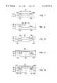
- FIG. 1is a cross-sectional view of an integrated-circuit assembly at an early stage of fabrication
- FIG. 2is a cross-sectional view of the FIG. 1 integrated-circuit assembly after formation of an insulative layer 18 including portions 18 a, 18 b, and 18 c;
- FIG. 3is a cross-sectional view of the FIG. 2 assembly after replacement of portions 18 a, 18 b, and 18 c with a filler material 20 and formation of holes 19 a and 19 b;
- FIG. 4is a cross-sectional view of the FIG. 3 assembly after formation of an aluminum-beryllium layer 22 on material 20 and in holes 19 a and 19 b;
- FIG. 5is a cross-sectional view of the FIG. 4 assembly after patterning layer 22 into a conductor 22 ′ and removing filler material 20 to form cavity 20 ′;
- FIG. 6is a block diagram of a generic integrated memory circuit incorporating one or more air bridges of the present invention.
- FIGS. 1-6describes and illustrates one or more specific embodiments of the invention. These embodiments, offered not to limit but only to exemplify and teach the invention, are shown and described in sufficient detail to enable those skilled in the art to practice the invention. Thus, where appropriate to avoid obscuring the invention, the description may omit certain information known to those of skill in the art.
- substrateencompasses a semiconductor wafer as well as structures having one or more insulative, semi-insulative, conductive, or semiconductive layers and materials.
- the termembraces silicon-on-insulator, silicon-on-sapphire, and other advanced structures.
- cavityrefers to a bounded, three-dimensional region having a dielectric constant different from areas outside the region.
- the term “cavity”encompasses gas-filled regions, liquid-filled regions, gas-liquid-filled regions, porous regions, and vacuum regions.
- percentin the context of a material composition refers to weight percent unless otherwise noted.
- FIGS. 1-6show a number of exemplary integrated-circuit assemblies, which taken collectively and sequentially, illustrate an exemplary method of fabricating an integrated circuit including an extra-long air bridge consistent with the present invention.
- the methodas shown in FIG. 1, a cross-sectional view, begins with a known integrated-circuit assembly or structure 10 , which may reside within any integrated circuit, for example, an otherwise conventional integrated memory circuit.
- Assembly 10includes a substrate 12 , which supports a number of integrated elements 14 , particularly transistors 14 a and 14 b. Transistors 14 a and 14 b are covered by a 100-nanometer-thick, insulative layer 16 , which for example consists of a silicon oxide, nitride, or oxynitride. Layer 16 includes two tungsten vias (or contact plugs) 16 a and 16 b electrically connected to respective transistors 14 a and 14 b. Although omitted from FIGS. 1-5 for clarity, assembly 10 , in some embodiments, includes a titanium-nitride (TiN) diffusion barrier between vias 16 a and 16 b and transistors 14 a and 14 b.
- TiNtitanium-nitride
- Transistors 14 a and 14 b and corresponding vias 16 a and 16 bare separated by a distance 15 of 1.4 millimeters, which is approximately 40 percent longer than the one-millimeter maximum free-span length of conventional aluminum-alloy air bridges, assuming a 500 nanometer thickness and a maximum allowable sag of 250 nanometers.
- a distance 15 of 1.4 millimeterswhich is approximately 40 percent longer than the one-millimeter maximum free-span length of conventional aluminum-alloy air bridges, assuming a 500 nanometer thickness and a maximum allowable sag of 250 nanometers.
- One of skill in the artunderstands that using different thicknesses, maximum-allowable sags, and/or breaking-point constraints would provide other maximum free-span lengths, both greater and less than the strictly exemplary 1.4 millimeters mentioned here.
- FIG. 2shows the beginning of the exemplary air-bridge fabrication method.
- the methoddeposits or grows an insulative material layer 18 atop layer 16 .
- suitable insulative materialinclude photoresist and silicon dioxide.
- Layer 18includes three portions 18 a, 18 b, and 18 c.
- FIG. 3shows that the method next entails removing portions 18 a, 18 b, and 18 c, using any selective-material-removal technique, etching for example. Then, the spaces previously occupied by portions 18 a - 18 c are filled with a sacrificial filler material 20 and subsequently planarized. Examples of suitable filler material include silicon nitride and numerous polymers. Other embodiments leave portion 18 b to serve as an intermediate air-bridge support, facilitating construction of longer and/or thinner bridges. Two holes 19 a and 19 b, which will define conductive air-bridge supports, are also formed in layer 18 , exposing portions of respective vias 16 a and 16 b.
- the methodforms a 500-nanometer-thick aluminum-beryllium (Al—Be) layer 22 over the first insulative layer 18 and filler material 20 and into holes 19 a and 19 b.
- aluminum-beryllium layer 22consists essentially of 25% beryllium and 0.5% copper, with the remainder being aluminum and reasonably unavoidable impurities. (Commercially available raw aluminum, which is about 99% pure, generally contains negligible quantities of iron, silicon, and other impurities.)
- This particular alloyhas a density ( ⁇ ) of approximately 2.42 Mg/m 3 , a Young's Modulus of Elasticity (E) of approximately 99 GPa, and an electrical resistance of 31.3 n ⁇ m.
- the ratio of elasticity to density (E/ ⁇ ), a measure of rigidity,is approximately 40.9 GPam 3 /Mg.
- the aluminum-silicon-copper alloy common to most internal integrated-circuit conductors1% copper and 0.5% silicon
- the maximum free-span length, based on break point or maximum allowable sagis proportional to the E/ ⁇ for the bridge metal. More precisely, the maximum free-span length, for most practical integrated-circuit applications, adheres to the following approximation:
- Ldenotes the free-span length
- Edenotes the modulus of elasticity of the bridge alloy
- ⁇ (delta)denotes the maximum allowable deflection, or sag, of the bridge
- ⁇ (rho)is the bridge-alloy density
- tis the thickness of the bridge (in the deflection direction).
- Aluminum-beryllium layer 22may be formed using a wide variety of techniques.
- the exemplary embodimentforms the layer using conventional sputtering from an alloy target of the desired composition.
- Other embodimentsfollow a layered approach which uses two targets, one of beryllium and the other of aluminum, aluminum-copper, aluminum-titanium or aluminum-copper-titanium. In this approach, one or more layers of each target material are used to realize the desired composition. And, still other embodiments use chemical-vapor deposition or even jet-vapor deposition.
- the present inventionis not restricted to any particular method or class of methods for forming aluminum-beryllium layer 22 .
- FIG. 5shows the results of the next series of operations.
- aluminum-beryllium layer 22is patterned to form a 167-nanometer-wide aluminum-beryllium air-bridge conductor 22 ′ that includes end supports 22 a ′ and 22 b ′.
- the exemplary embodimentuses conventional photolithography and etching to form the aluminum-beryllium conductor from layer 22 .
- other embodimentsfollow a single- or dual-damascene approach which generally entails etching a trench in layer 18 and material, filling the trench with the aluminum-beryllium alloy, and then removing excess alloy to form the conductor.
- the exemplary embodimentsprovides conductor 22 ′ with a rectangular cross-section and a height-to-width, or aspect, ratio of 3:1.
- Other embodimentsgenerally less suitable to mass production, form the conductor with any number of alternative aspect ratios as well as cross-sectional sizes and shapes.
- one embodimentprovides conductor 22 ′ with a 4:1 aspect ratio, and another provides conductor 22 ′ with a square shape.
- the methodremoves filler material 20 to leave a cavity 20 ′ underneath air-bridge conductor 22 ′.
- Cavity 20 ′ in the exemplary embodimentis filled with air.
- other embodimentsfill the cavity with other gases, or even a porous insulator.
- Examples of other air-bridge structures which would benefit from incorporating one or more alloys of the present inventioninclude double- and triple-wide and multilevel bridge structures. These and other structures are disclosed in co-assigned U.S. patent application Ser. No. 08/954,450, which was filed on Oct. 20, 1997, now U.S. Pat. No. 5,891,797 and is incorporated herein by reference. Moreover, the alloys may be used with other air-bridge fabrication methods. See, for example, U.S. Pat. No. 5,510,645 entitled Semiconductor Structures Having an Air Region and Method of Forming the Semiconductor Structure and U.S. Pat. No. 5,324,684 entitled Method of Forming Semiconductor Structure Having an Air Region, both incorporated herein by reference.
- FIG. 6shows one example of the unlimited number of integrated circuits which would benefit from incorporation of the aluminum-beryllium air bridges of the present invention: a generic integrated memory circuit 40 .
- Memory circuit 40which operates according to well-known and understood principles, is generally coupled to a processor (not shown) to form a computer system. More particularly, circuit 40 includes a memory array 42 which comprises a number of memory cells 43 , a column address decoder 44 , and a row address decoder 45 , bit lines 46 , word lines 47 , and voltage-sense-amplifier circuit 48 coupled in conventional fashion to bit lines 46 .
- the memory cells, the address decoders, and amplifier circuitare interconnected via at least one aluminum-beryllium air bridge of the present invention.
- the memory array 42 and voltage-sense-amplifier circuit 48are interconnected via aluminum-beryllium air-bridges.
- the inventorhas developed new aluminum-beryllium alloys which compared to conventional aluminum alloys have superior rigidity and comparable electrical resistance.
- One of thesewhich is about 60 percent more rigid and only about 10 percent more electrical resistive than the conventional aluminum alloy, allows construction of air bridges that are 40 percent longer. This advantage ultimately translates into integrated circuits with superior speed and efficiency.
Landscapes
- Engineering & Computer Science (AREA)
- Power Engineering (AREA)
- General Physics & Mathematics (AREA)
- Condensed Matter Physics & Semiconductors (AREA)
- Computer Hardware Design (AREA)
- Microelectronics & Electronic Packaging (AREA)
- Physics & Mathematics (AREA)
- Chemical & Material Sciences (AREA)
- Materials Engineering (AREA)
- Mechanical Engineering (AREA)
- Metallurgy (AREA)
- Organic Chemistry (AREA)
- Internal Circuitry In Semiconductor Integrated Circuit Devices (AREA)
Abstract
Description
| TABLE 1 |
| Aluminum Alloys with Enhanced Rigidity and Low Resistance |
| Beryllium % | Copper % | Titanium % |
| 1-40 | 0-6 | 0-2 |
| 1-40 | 0.2-2 | 0-2 |
| 1-40 | 0-6 | 0.5-1 |
| 1-40 | 0-6 | <0.1 |
| 1-40 | 0.2-1 | <0.1 |
| 15-30 | 0-6 | 0-2 |
| 15-30 | 0.2-2 | 0-2 |
| 20-30 | 0.2-1 | <0.1 |
| 20-30 | 0.4-0.6 | <0.1 |
| 20-30 | 0.4-0.6 | 0-2 |
| 24-26 | 0.4-0.6 | <0.1 |
Claims (29)
Priority Applications (3)
| Application Number | Priority Date | Filing Date | Title |
|---|---|---|---|
| US09/119,355US6509590B1 (en) | 1998-07-20 | 1998-07-20 | Aluminum-beryllium alloys for air bridges |
| US10/349,015US6717191B2 (en) | 1998-07-20 | 2003-01-21 | Aluminum-beryllium alloys for air bridges |
| US10/819,025US6943090B2 (en) | 1998-07-20 | 2004-04-06 | Aluminum-beryllium alloys for air bridges |
Applications Claiming Priority (1)
| Application Number | Priority Date | Filing Date | Title |
|---|---|---|---|
| US09/119,355US6509590B1 (en) | 1998-07-20 | 1998-07-20 | Aluminum-beryllium alloys for air bridges |
Related Child Applications (1)
| Application Number | Title | Priority Date | Filing Date |
|---|---|---|---|
| US10/349,015ContinuationUS6717191B2 (en) | 1998-07-20 | 2003-01-21 | Aluminum-beryllium alloys for air bridges |
Publications (1)
| Publication Number | Publication Date |
|---|---|
| US6509590B1true US6509590B1 (en) | 2003-01-21 |
Family
ID=22383954
Family Applications (3)
| Application Number | Title | Priority Date | Filing Date |
|---|---|---|---|
| US09/119,355Expired - LifetimeUS6509590B1 (en) | 1998-07-20 | 1998-07-20 | Aluminum-beryllium alloys for air bridges |
| US10/349,015Expired - Fee RelatedUS6717191B2 (en) | 1998-07-20 | 2003-01-21 | Aluminum-beryllium alloys for air bridges |
| US10/819,025Expired - Fee RelatedUS6943090B2 (en) | 1998-07-20 | 2004-04-06 | Aluminum-beryllium alloys for air bridges |
Family Applications After (2)
| Application Number | Title | Priority Date | Filing Date |
|---|---|---|---|
| US10/349,015Expired - Fee RelatedUS6717191B2 (en) | 1998-07-20 | 2003-01-21 | Aluminum-beryllium alloys for air bridges |
| US10/819,025Expired - Fee RelatedUS6943090B2 (en) | 1998-07-20 | 2004-04-06 | Aluminum-beryllium alloys for air bridges |
Country Status (1)
| Country | Link |
|---|---|
| US (3) | US6509590B1 (en) |
Cited By (3)
| Publication number | Priority date | Publication date | Assignee | Title |
|---|---|---|---|---|
| US20020172726A1 (en)* | 2000-04-18 | 2002-11-21 | Hideo Hosono | 12cao . 7a12o3 compound clathrating active oxygen species and method for preparing the same |
| US20030034559A1 (en)* | 2001-08-14 | 2003-02-20 | Siliconware Precision Industries Co., Ltd. | Ball grid array package with electrically-conductive bridge |
| US20040014273A1 (en)* | 2002-07-18 | 2004-01-22 | Micron Technology, Inc. | Techniques to create low K ILD for BEOL |
Families Citing this family (9)
| Publication number | Priority date | Publication date | Assignee | Title |
|---|---|---|---|---|
| US6429120B1 (en) | 2000-01-18 | 2002-08-06 | Micron Technology, Inc. | Methods and apparatus for making integrated-circuit wiring from copper, silver, gold, and other metals |
| US6303423B1 (en)* | 1998-12-21 | 2001-10-16 | Megic Corporation | Method for forming high performance system-on-chip using post passivation process |
| US6420262B1 (en) | 2000-01-18 | 2002-07-16 | Micron Technology, Inc. | Structures and methods to enhance copper metallization |
| US7262130B1 (en) | 2000-01-18 | 2007-08-28 | Micron Technology, Inc. | Methods for making integrated-circuit wiring from copper, silver, gold, and other metals |
| US6674167B1 (en) | 2000-05-31 | 2004-01-06 | Micron Technology, Inc. | Multilevel copper interconnect with double passivation |
| JP2006024698A (en)* | 2004-07-07 | 2006-01-26 | Toshiba Corp | Semiconductor device and manufacturing method thereof |
| WO2009100436A2 (en)* | 2008-02-10 | 2009-08-13 | Empire Magnetics Inc. | Winding for an axial gap electro dynamo machine |
| US20190252243A1 (en)* | 2018-02-12 | 2019-08-15 | Duet Microelectronics Inc. | Method of manufacturing airbridges for high performance semiconductor device |
| US20240355738A1 (en)* | 2023-04-21 | 2024-10-24 | Wolfspeed, Inc. | Power Semiconductor Devices Including Beryllium Metallization |
Citations (48)
| Publication number | Priority date | Publication date | Assignee | Title |
|---|---|---|---|---|
| US1254987A (en) | 1917-10-15 | 1918-01-29 | Cooper Res Company | Alloy. |
| US1976375A (en) | 1931-01-27 | 1934-10-09 | Beryllium Corp | Beryllium-aluminum alloy and method of heat treating the same |
| US2244608A (en) | 1939-02-09 | 1941-06-03 | Cooper Wilford Beryllium Ltd | Process of making alloys of aluminum beryllium |
| US3147110A (en) | 1961-11-27 | 1964-09-01 | Dow Chemical Co | Die-expressed article of aluminum-base alloy and method of making |
| US3337334A (en) | 1963-12-06 | 1967-08-22 | Lockheed Aircraft Corp | Beryllium-aluminum alloy |
| US3506438A (en) | 1967-07-24 | 1970-04-14 | Mallory & Co Inc P R | Method of producing beryllium composites by liquid phase sintering |
| US3548915A (en) | 1969-06-11 | 1970-12-22 | Mallory & Co Inc P R | New procedure for chill casting beryllium composite |
| US3548948A (en) | 1969-01-23 | 1970-12-22 | Mallory & Co Inc P R | Procedure for chill casting beryllium composite |
| US3687737A (en) | 1970-07-17 | 1972-08-29 | Mallory & Co Inc P R | Method of making beryllium-aluminum-copper-silicon wrought material |
| US3832456A (en)* | 1962-10-18 | 1974-08-27 | Ethyl Corp | Process for the manufacture of beryllium hydride |
| US3923500A (en)* | 1971-08-11 | 1975-12-02 | Toyo Valve Co Ltd | Copper base alloy |
| US4022931A (en) | 1974-07-01 | 1977-05-10 | Motorola, Inc. | Process for making semiconductor device |
| US4029377A (en) | 1976-02-03 | 1977-06-14 | Rogers Corporation | Push-on bus bar |
| US4065330A (en)* | 1974-09-26 | 1977-12-27 | The Foundation: The Research Institute Of Electric And Magnetic Alloys | Wear-resistant high-permeability alloy |
| US4101855A (en)* | 1976-11-05 | 1978-07-18 | Hi-G Incorporated | Miniature relay |
| US4158719A (en) | 1977-06-09 | 1979-06-19 | Carpenter Technology Corporation | Low expansion low resistivity composite powder metallurgy member and method of making the same |
| US4233066A (en)* | 1972-04-27 | 1980-11-11 | Aktiebolaget Elektrokoppar | Electrical conductor of aluminium |
| US4314594A (en)* | 1977-02-26 | 1982-02-09 | Vacuumschmelze Gmbh | Reducing magnetic hysteresis losses in cores of thin tapes of soft magnetic amorphous metal alloys |
| US4389429A (en) | 1980-06-16 | 1983-06-21 | Rockwell International Corporation | Method of forming integrated circuit chip transmission line |
| US4561173A (en) | 1978-11-14 | 1985-12-31 | U.S. Philips Corporation | Method of manufacturing a wiring system |
| US4709359A (en)* | 1982-06-28 | 1987-11-24 | Magnovox Government And Industrial Electronics Company | End weighted reed sound transducer |
| US5045635A (en)* | 1989-06-16 | 1991-09-03 | Schlegel Corporation | Conductive gasket with flame and abrasion resistant conductive coating |
| US5148260A (en) | 1989-09-07 | 1992-09-15 | Kabushiki Kaisha Toshiba | Semiconductor device having an improved air-bridge lead structure |
| US5231036A (en)* | 1990-12-07 | 1993-07-27 | Kyocera America, Inc. | Method of using a contamination shield during the manufacture of EPROM semiconductor package windows |
| US5324683A (en) | 1993-06-02 | 1994-06-28 | Motorola, Inc. | Method of forming a semiconductor structure having an air region |
| US5324684A (en) | 1992-02-25 | 1994-06-28 | Ag Processing Technologies, Inc. | Gas phase doping of semiconductor material in a cold-wall radiantly heated reactor under reduced pressure |
| US5336914A (en) | 1991-06-19 | 1994-08-09 | Nec Corporation | Static semiconductor memory device |
| US5399897A (en)* | 1993-11-29 | 1995-03-21 | Raytheon Company | Microstructure and method of making such structure |
| US5408742A (en) | 1991-10-28 | 1995-04-25 | Martin Marietta Corporation | Process for making air bridges for integrated circuits |
| US5424030A (en) | 1992-12-03 | 1995-06-13 | Yamaha Metanix Corporation | Copper alloy for fine pattern lead frame |
| US5444015A (en) | 1992-12-15 | 1995-08-22 | International Business Machines Corporation | Larce scale IC personalization method employing air dielectric structure for extended conductors |
| US5457344A (en) | 1994-03-25 | 1995-10-10 | Bartelink; Dirk J. | Test fixtures for C4 solder-bump technology |
| US5485032A (en)* | 1992-12-18 | 1996-01-16 | International Business Machines Corporation | Antifuse element with electrical or optical programming |
| US5578146A (en) | 1991-10-02 | 1996-11-26 | Brush Wellman, Inc. | Aluminum-beryllium alloys having high stiffness and low thermal expansion for memory devices |
| US5667600A (en)* | 1991-10-02 | 1997-09-16 | Brush Wellman, Inc. | Aluminum alloys containing beryllium and investment casting of such alloys |
| US5725689A (en) | 1994-03-28 | 1998-03-10 | Nippon Steel Corporation | Steel wire of high strength excellent in fatigue characteristics |
| US5852871A (en)* | 1993-11-16 | 1998-12-29 | Form Factor, Inc. | Method of making raised contacts on electronic components |
| US5891797A (en)* | 1997-10-20 | 1999-04-06 | Micron Technology, Inc. | Method of forming a support structure for air bridge wiring of an integrated circuit |
| US6015738A (en)* | 1994-05-05 | 2000-01-18 | California Institute Of Technology | Method for fabricating transistorless, multistable current-mode memory cells and memory arrays |
| US6025261A (en)* | 1998-04-29 | 2000-02-15 | Micron Technology, Inc. | Method for making high-Q inductive elements |
| US6057226A (en)* | 1997-11-25 | 2000-05-02 | Intel Corporation | Air gap based low dielectric constant interconnect structure and method of making same |
| US6075287A (en)* | 1997-04-03 | 2000-06-13 | International Business Machines Corporation | Integrated, multi-chip, thermally conductive packaging device and methodology |
| US6075278A (en)* | 1997-04-24 | 2000-06-13 | Micron Technology, Inc. | Aluminum based alloy bridge structure and method of forming same |
| US6091475A (en)* | 1996-12-19 | 2000-07-18 | Shin-Etsu Polymer Co., Ltd. | Connector for display inspection of a liquid crystal display panel and method for the preparation thereof |
| US6204065B1 (en) | 1997-03-27 | 2001-03-20 | Ngk Insulators, Ltd. | Conduction assist member and manufacturing method of the same |
| US6265811B1 (en)* | 1996-11-29 | 2001-07-24 | Ngk Insulators, Ltd. | Ceramic element, method for producing ceramic element, display device, relay device and capacitor |
| US6288905B1 (en)* | 1999-04-15 | 2001-09-11 | Amerasia International Technology Inc. | Contact module, as for a smart card, and method for making same |
| US20010054771A1 (en)* | 1997-03-26 | 2001-12-27 | Wark James M. | Method for making projected contact structures for engaging bumped semiconductor devices |
Family Cites Families (3)
| Publication number | Priority date | Publication date | Assignee | Title |
|---|---|---|---|---|
| US5000818A (en)* | 1989-08-14 | 1991-03-19 | Fairchild Semiconductor Corporation | Method of fabricating a high performance interconnect system for an integrated circuit |
| US5171713A (en)* | 1990-01-10 | 1992-12-15 | Micrunity Systems Eng | Process for forming planarized, air-bridge interconnects on a semiconductor substrate |
| US5482898A (en)* | 1993-04-12 | 1996-01-09 | Amkor Electronics, Inc. | Method for forming a semiconductor device having a thermal dissipator and electromagnetic shielding |
- 1998
- 1998-07-20USUS09/119,355patent/US6509590B1/ennot_activeExpired - Lifetime
- 2003
- 2003-01-21USUS10/349,015patent/US6717191B2/ennot_activeExpired - Fee Related
- 2004
- 2004-04-06USUS10/819,025patent/US6943090B2/ennot_activeExpired - Fee Related
Patent Citations (50)
| Publication number | Priority date | Publication date | Assignee | Title |
|---|---|---|---|---|
| US1254987A (en) | 1917-10-15 | 1918-01-29 | Cooper Res Company | Alloy. |
| US1976375A (en) | 1931-01-27 | 1934-10-09 | Beryllium Corp | Beryllium-aluminum alloy and method of heat treating the same |
| US2244608A (en) | 1939-02-09 | 1941-06-03 | Cooper Wilford Beryllium Ltd | Process of making alloys of aluminum beryllium |
| US3147110A (en) | 1961-11-27 | 1964-09-01 | Dow Chemical Co | Die-expressed article of aluminum-base alloy and method of making |
| US3832456A (en)* | 1962-10-18 | 1974-08-27 | Ethyl Corp | Process for the manufacture of beryllium hydride |
| US3337334A (en) | 1963-12-06 | 1967-08-22 | Lockheed Aircraft Corp | Beryllium-aluminum alloy |
| US3506438A (en) | 1967-07-24 | 1970-04-14 | Mallory & Co Inc P R | Method of producing beryllium composites by liquid phase sintering |
| US3548948A (en) | 1969-01-23 | 1970-12-22 | Mallory & Co Inc P R | Procedure for chill casting beryllium composite |
| US3548915A (en) | 1969-06-11 | 1970-12-22 | Mallory & Co Inc P R | New procedure for chill casting beryllium composite |
| US3687737A (en) | 1970-07-17 | 1972-08-29 | Mallory & Co Inc P R | Method of making beryllium-aluminum-copper-silicon wrought material |
| US3923500A (en)* | 1971-08-11 | 1975-12-02 | Toyo Valve Co Ltd | Copper base alloy |
| US4233066A (en)* | 1972-04-27 | 1980-11-11 | Aktiebolaget Elektrokoppar | Electrical conductor of aluminium |
| US4022931A (en) | 1974-07-01 | 1977-05-10 | Motorola, Inc. | Process for making semiconductor device |
| US4065330A (en)* | 1974-09-26 | 1977-12-27 | The Foundation: The Research Institute Of Electric And Magnetic Alloys | Wear-resistant high-permeability alloy |
| US4029377A (en) | 1976-02-03 | 1977-06-14 | Rogers Corporation | Push-on bus bar |
| US4101855A (en)* | 1976-11-05 | 1978-07-18 | Hi-G Incorporated | Miniature relay |
| US4314594A (en)* | 1977-02-26 | 1982-02-09 | Vacuumschmelze Gmbh | Reducing magnetic hysteresis losses in cores of thin tapes of soft magnetic amorphous metal alloys |
| US4158719A (en) | 1977-06-09 | 1979-06-19 | Carpenter Technology Corporation | Low expansion low resistivity composite powder metallurgy member and method of making the same |
| US4561173A (en) | 1978-11-14 | 1985-12-31 | U.S. Philips Corporation | Method of manufacturing a wiring system |
| US4389429A (en) | 1980-06-16 | 1983-06-21 | Rockwell International Corporation | Method of forming integrated circuit chip transmission line |
| US4709359A (en)* | 1982-06-28 | 1987-11-24 | Magnovox Government And Industrial Electronics Company | End weighted reed sound transducer |
| US5045635A (en)* | 1989-06-16 | 1991-09-03 | Schlegel Corporation | Conductive gasket with flame and abrasion resistant conductive coating |
| US5148260A (en) | 1989-09-07 | 1992-09-15 | Kabushiki Kaisha Toshiba | Semiconductor device having an improved air-bridge lead structure |
| US5231036A (en)* | 1990-12-07 | 1993-07-27 | Kyocera America, Inc. | Method of using a contamination shield during the manufacture of EPROM semiconductor package windows |
| US5336914A (en) | 1991-06-19 | 1994-08-09 | Nec Corporation | Static semiconductor memory device |
| US5667600A (en)* | 1991-10-02 | 1997-09-16 | Brush Wellman, Inc. | Aluminum alloys containing beryllium and investment casting of such alloys |
| US5578146A (en) | 1991-10-02 | 1996-11-26 | Brush Wellman, Inc. | Aluminum-beryllium alloys having high stiffness and low thermal expansion for memory devices |
| US5408742A (en) | 1991-10-28 | 1995-04-25 | Martin Marietta Corporation | Process for making air bridges for integrated circuits |
| US5324684A (en) | 1992-02-25 | 1994-06-28 | Ag Processing Technologies, Inc. | Gas phase doping of semiconductor material in a cold-wall radiantly heated reactor under reduced pressure |
| US5424030A (en) | 1992-12-03 | 1995-06-13 | Yamaha Metanix Corporation | Copper alloy for fine pattern lead frame |
| US5444015A (en) | 1992-12-15 | 1995-08-22 | International Business Machines Corporation | Larce scale IC personalization method employing air dielectric structure for extended conductors |
| US5485032A (en)* | 1992-12-18 | 1996-01-16 | International Business Machines Corporation | Antifuse element with electrical or optical programming |
| US5324683A (en) | 1993-06-02 | 1994-06-28 | Motorola, Inc. | Method of forming a semiconductor structure having an air region |
| US5510645A (en)* | 1993-06-02 | 1996-04-23 | Motorola, Inc. | Semiconductor structure having an air region and method of forming the semiconductor structure |
| US5852871A (en)* | 1993-11-16 | 1998-12-29 | Form Factor, Inc. | Method of making raised contacts on electronic components |
| US5399897A (en)* | 1993-11-29 | 1995-03-21 | Raytheon Company | Microstructure and method of making such structure |
| US5457344A (en) | 1994-03-25 | 1995-10-10 | Bartelink; Dirk J. | Test fixtures for C4 solder-bump technology |
| US5725689A (en) | 1994-03-28 | 1998-03-10 | Nippon Steel Corporation | Steel wire of high strength excellent in fatigue characteristics |
| US6015738A (en)* | 1994-05-05 | 2000-01-18 | California Institute Of Technology | Method for fabricating transistorless, multistable current-mode memory cells and memory arrays |
| US6265811B1 (en)* | 1996-11-29 | 2001-07-24 | Ngk Insulators, Ltd. | Ceramic element, method for producing ceramic element, display device, relay device and capacitor |
| US6091475A (en)* | 1996-12-19 | 2000-07-18 | Shin-Etsu Polymer Co., Ltd. | Connector for display inspection of a liquid crystal display panel and method for the preparation thereof |
| US20010054771A1 (en)* | 1997-03-26 | 2001-12-27 | Wark James M. | Method for making projected contact structures for engaging bumped semiconductor devices |
| US6204065B1 (en) | 1997-03-27 | 2001-03-20 | Ngk Insulators, Ltd. | Conduction assist member and manufacturing method of the same |
| US6075287A (en)* | 1997-04-03 | 2000-06-13 | International Business Machines Corporation | Integrated, multi-chip, thermally conductive packaging device and methodology |
| US6075278A (en)* | 1997-04-24 | 2000-06-13 | Micron Technology, Inc. | Aluminum based alloy bridge structure and method of forming same |
| US5994777A (en)* | 1997-10-20 | 1999-11-30 | Micron Technology, Inc. | Method and support structure for air bridge wiring of an integrated circuit |
| US5891797A (en)* | 1997-10-20 | 1999-04-06 | Micron Technology, Inc. | Method of forming a support structure for air bridge wiring of an integrated circuit |
| US6057226A (en)* | 1997-11-25 | 2000-05-02 | Intel Corporation | Air gap based low dielectric constant interconnect structure and method of making same |
| US6025261A (en)* | 1998-04-29 | 2000-02-15 | Micron Technology, Inc. | Method for making high-Q inductive elements |
| US6288905B1 (en)* | 1999-04-15 | 2001-09-11 | Amerasia International Technology Inc. | Contact module, as for a smart card, and method for making same |
Non-Patent Citations (6)
| Title |
|---|
| "Phase Diagrams", Metals Handbook, 10th Ed., vol. 3, (1992). |
| "Properties and Selection: Nonferrous Alloys and Pure Metals", Metals Handbook, 9th ed., vol. 2, (1979). |
| Dudzinski, N., et al., "The Youngs Modulus of Some Aluminim Alloys", J. Institute of Metals, vol. LXXIV, pp. 291-314, (1947-48). |
| Singer, F.L., Strength of Materials, Harper & Brothers, 229-32, (1951). |
| Van Horn, K.R., "Aluminim Vol. 1 Properties Physical Metallurgy and Phase Diagrams", American Society for Metals, Metals Park, OH, (1967). |
| Wolf, S., "Chapter 4: Multilevel-Interconnect Technology for VLSI and ULSI", In: Silicon Processing for the VLSI Era, vol. 2 Process Integration, Lattice Press, Sunset Beach, CA, 176-297, (1990). |
Cited By (10)
| Publication number | Priority date | Publication date | Assignee | Title |
|---|---|---|---|---|
| US20020172726A1 (en)* | 2000-04-18 | 2002-11-21 | Hideo Hosono | 12cao . 7a12o3 compound clathrating active oxygen species and method for preparing the same |
| US20030034559A1 (en)* | 2001-08-14 | 2003-02-20 | Siliconware Precision Industries Co., Ltd. | Ball grid array package with electrically-conductive bridge |
| US20040014273A1 (en)* | 2002-07-18 | 2004-01-22 | Micron Technology, Inc. | Techniques to create low K ILD for BEOL |
| US20050026388A1 (en)* | 2002-07-18 | 2005-02-03 | Micron Technology, Inc. | Techniques to create low K ILD for BEOL |
| US20050029609A1 (en)* | 2002-07-18 | 2005-02-10 | Micron Technology, Inc. | Techniques to create low K ILD for beol |
| US6903001B2 (en) | 2002-07-18 | 2005-06-07 | Micron Technology Inc. | Techniques to create low K ILD for BEOL |
| US20060292858A1 (en)* | 2002-07-18 | 2006-12-28 | Micron Technology, Inc. | Techniques to create low K ILD for beol |
| US7157387B2 (en) | 2002-07-18 | 2007-01-02 | Micron Technologies, Inc. | Techniques to create low K ILD for BEOL |
| US7190043B2 (en) | 2002-07-18 | 2007-03-13 | Micron Technology, Inc. | Techniques to create low K ILD for beol |
| US7492030B2 (en) | 2002-07-18 | 2009-02-17 | Micron Technology, Inc. | Techniques to create low K ILD forming voids between metal lines |
Also Published As
| Publication number | Publication date |
|---|---|
| US20030127741A1 (en) | 2003-07-10 |
| US20040192020A1 (en) | 2004-09-30 |
| US6943090B2 (en) | 2005-09-13 |
| US6717191B2 (en) | 2004-04-06 |
Similar Documents
| Publication | Publication Date | Title |
|---|---|---|
| US6509590B1 (en) | Aluminum-beryllium alloys for air bridges | |
| US7572682B2 (en) | Semiconductor structure for fuse and anti-fuse applications | |
| US5663590A (en) | Product of process for formation of vias (or contact openings) and fuses in the same insulation layer with minimal additional steps | |
| US5786268A (en) | Method for forming programmable interconnect structures and programmable integrated circuits | |
| US5557136A (en) | Programmable interconnect structures and programmable integrated circuits | |
| US8749020B2 (en) | Metal e-fuse structure design | |
| JP3778487B2 (en) | Method for forming metal capacitor | |
| US5633198A (en) | Method of forming wiring with gaps in bend to improve electromigration resistance | |
| JP5558662B2 (en) | Device, Method (MIM Capacitor and Method for Manufacturing the Same) | |
| US6614099B2 (en) | Copper metallurgy in integrated circuits | |
| KR19990072753A (en) | Semiconductor device and fabrication method thereof | |
| US8610244B2 (en) | Layered structure with fuse | |
| US20010005057A1 (en) | Process for making integrated circuit structure with thin dielectric between at least local interconnect level and first metal interconnect level | |
| EP0317161A2 (en) | Semiconductor memory device having an aluminium-based metallization film and a refractory metal silicide-based metallization film | |
| KR20020074202A (en) | Process for providing seed layers for aluminium, copper, gold and silver metallurgy | |
| JPH1174268A (en) | Integrated circuit and its manufacture | |
| CN1305118C (en) | Structural reinforcement of highly porous low k dielectric films by ILD posts | |
| JP2001298084A (en) | Damascene wiring structure and semiconductor device having damascene wiring | |
| KR20160005001A (en) | Electronic fuse having a damaged region | |
| US20020145201A1 (en) | Method and apparatus for making air gap insulation for semiconductor devices | |
| CN100570873C (en) | Capacitor and forming method thereof | |
| GB2390223A (en) | Capacitor for a semiconductor device and method of manufacture | |
| US6812571B2 (en) | Low capacitance wiring layout and method for making same | |
| US6075293A (en) | Semiconductor device having a multi-layer metal interconnect structure | |
| US20030141568A1 (en) | Semiconductor device and manufacturing method thereof |
Legal Events
| Date | Code | Title | Description |
|---|---|---|---|
| AS | Assignment | Owner name:MICRON TECHNOLOGY, INC., IDAHO Free format text:ASSIGNMENT OF ASSIGNORS INTEREST;ASSIGNOR:FARRAR, PAUL A.;REEL/FRAME:009332/0383 Effective date:19980707 | |
| FEPP | Fee payment procedure | Free format text:PAYOR NUMBER ASSIGNED (ORIGINAL EVENT CODE: ASPN); ENTITY STATUS OF PATENT OWNER: LARGE ENTITY | |
| STCF | Information on status: patent grant | Free format text:PATENTED CASE | |
| FPAY | Fee payment | Year of fee payment:4 | |
| AS | Assignment | Owner name:MOSAID TECHNOLOGIES INCORPORATED, CANADA Free format text:ASSIGNMENT OF ASSIGNORS INTEREST;ASSIGNOR:MICRON TECHNOLOGY, INC.;REEL/FRAME:023438/0614 Effective date:20090609 | |
| FEPP | Fee payment procedure | Free format text:PAYER NUMBER DE-ASSIGNED (ORIGINAL EVENT CODE: RMPN); ENTITY STATUS OF PATENT OWNER: LARGE ENTITY Free format text:PAYOR NUMBER ASSIGNED (ORIGINAL EVENT CODE: ASPN); ENTITY STATUS OF PATENT OWNER: LARGE ENTITY | |
| FPAY | Fee payment | Year of fee payment:8 | |
| AS | Assignment | Owner name:ROYAL BANK OF CANADA, CANADA Free format text:U.S. INTELLECTUAL PROPERTY SECURITY AGREEMENT (FOR NON-U.S. GRANTORS) - SHORT FORM;ASSIGNORS:658276 N.B. LTD.;658868 N.B. INC.;MOSAID TECHNOLOGIES INCORPORATED;REEL/FRAME:027512/0196 Effective date:20111223 | |
| AS | Assignment | Owner name:CONVERSANT INTELLECTUAL PROPERTY MANAGEMENT INC., Free format text:CHANGE OF NAME;ASSIGNOR:MOSAID TECHNOLOGIES INCORPORATED;REEL/FRAME:032439/0638 Effective date:20140101 | |
| FPAY | Fee payment | Year of fee payment:12 | |
| AS | Assignment | Owner name:CONVERSANT IP N.B. 868 INC., CANADA Free format text:RELEASE OF SECURITY INTEREST;ASSIGNOR:ROYAL BANK OF CANADA;REEL/FRAME:033484/0344 Effective date:20140611 Owner name:CONVERSANT IP N.B. 276 INC., CANADA Free format text:RELEASE OF SECURITY INTEREST;ASSIGNOR:ROYAL BANK OF CANADA;REEL/FRAME:033484/0344 Effective date:20140611 Owner name:CONVERSANT INTELLECTUAL PROPERTY MANAGEMENT INC., Free format text:RELEASE OF SECURITY INTEREST;ASSIGNOR:ROYAL BANK OF CANADA;REEL/FRAME:033484/0344 Effective date:20140611 | |
| AS | Assignment | Owner name:CONVERSANT INTELLECTUAL PROPERTY MANAGEMENT INC., CANADA Free format text:CHANGE OF ADDRESS;ASSIGNOR:CONVERSANT INTELLECTUAL PROPERTY MANAGEMENT INC.;REEL/FRAME:033678/0096 Effective date:20140820 Owner name:CONVERSANT INTELLECTUAL PROPERTY MANAGEMENT INC., Free format text:CHANGE OF ADDRESS;ASSIGNOR:CONVERSANT INTELLECTUAL PROPERTY MANAGEMENT INC.;REEL/FRAME:033678/0096 Effective date:20140820 | |
| AS | Assignment | Owner name:CPPIB CREDIT INVESTMENTS INC., AS LENDER, CANADA Free format text:U.S. PATENT SECURITY AGREEMENT (FOR NON-U.S. GRANTORS);ASSIGNOR:CONVERSANT INTELLECTUAL PROPERTY MANAGEMENT INC.;REEL/FRAME:033706/0367 Effective date:20140611 Owner name:ROYAL BANK OF CANADA, AS LENDER, CANADA Free format text:U.S. PATENT SECURITY AGREEMENT (FOR NON-U.S. GRANTORS);ASSIGNOR:CONVERSANT INTELLECTUAL PROPERTY MANAGEMENT INC.;REEL/FRAME:033706/0367 Effective date:20140611 | |
| AS | Assignment | Owner name:CPPIB CREDIT INVESTMENTS, INC., CANADA Free format text:AMENDED AND RESTATED U.S. PATENT SECURITY AGREEMENT (FOR NON-U.S. GRANTORS);ASSIGNOR:CONVERSANT INTELLECTUAL PROPERTY MANAGEMENT INC.;REEL/FRAME:046900/0136 Effective date:20180731 | |
| AS | Assignment | Owner name:CONVERSANT INTELLECTUAL PROPERTY MANAGEMENT INC., CANADA Free format text:RELEASE OF U.S. PATENT AGREEMENT (FOR NON-U.S. GRANTORS);ASSIGNOR:ROYAL BANK OF CANADA, AS LENDER;REEL/FRAME:047645/0424 Effective date:20180731 Owner name:CONVERSANT INTELLECTUAL PROPERTY MANAGEMENT INC., Free format text:RELEASE OF U.S. PATENT AGREEMENT (FOR NON-U.S. GRANTORS);ASSIGNOR:ROYAL BANK OF CANADA, AS LENDER;REEL/FRAME:047645/0424 Effective date:20180731 | |
| AS | Assignment | Owner name:CONVERSANT INTELLECTUAL PROPERTY MANAGEMENT INC., CANADA Free format text:RELEASE BY SECURED PARTY;ASSIGNOR:CPPIB CREDIT INVESTMENTS INC.;REEL/FRAME:054372/0281 Effective date:20201028 |