US6509198B2 - Method of power IC inspection - Google Patents
Method of power IC inspectionDownload PDFInfo
- Publication number
- US6509198B2 US6509198B2US09/969,601US96960101AUS6509198B2US 6509198 B2US6509198 B2US 6509198B2US 96960101 AUS96960101 AUS 96960101AUS 6509198 B2US6509198 B2US 6509198B2
- Authority
- US
- United States
- Prior art keywords
- semiconductor substrate
- solution
- power ics
- power
- water
- Prior art date
- Legal status (The legal status is an assumption and is not a legal conclusion. Google has not performed a legal analysis and makes no representation as to the accuracy of the status listed.)
- Expired - Lifetime
Links
Images


Classifications
- H—ELECTRICITY
- H01—ELECTRIC ELEMENTS
- H01L—SEMICONDUCTOR DEVICES NOT COVERED BY CLASS H10
- H01L22/00—Testing or measuring during manufacture or treatment; Reliability measurements, i.e. testing of parts without further processing to modify the parts as such; Structural arrangements therefor
- H01L22/20—Sequence of activities consisting of a plurality of measurements, corrections, marking or sorting steps
- H01L22/24—Optical enhancement of defects or not directly visible states, e.g. selective electrolytic deposition, bubbles in liquids, light emission, colour change
Definitions
- the present inventionrelates to a method of power IC inspection, more particularly, to a method applied to inspect whether electrically-failed power ICs results from photo resist peeling before or during source implantation.
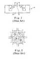
- FIG. 1 and FIG. 2represent the schematic cross-sectional diagram and top-view diagram of power ICs, respectively.
- the power ICis formed on a semiconductor substrate 10 .
- the gate 12 of the power ICis formed in a deep trench by performing a series of conventional photolithography, anisotropic etching step, and chemical vapor deposition.
- the source 14 of the power IC 14is formed by first coating a photo resist layer 16 , defining the region of source 14 by photolithography process, and then ion-implanting N-impurities (for NMOS) or P-impurities (for PMOS) into the semiconductor substrate 10 .
- the undoped region 18 between source and drainis not ion-implanted because the photo resist layer 16 serves as a hard mask during source implantation.
- the photo resist layer 16might peel during the photolithography process.
- the undoped region 18is ion-implanted during source implantation because of no hard mask.
- the breakdown voltage of source 14 to drain 20is too poor to well work.
- the main purpose of the present inventionis to provide a method of power IC inspection to inspect whether a electrically-failed portion of power ICs results from photo resist peeling during photolithography process during source implantation process.
- the present inventionprovides a method of power IC inspection to inspect whether electrically-failed power ICs results from photo resist peeling during source implantation.
- the hot spots on the semiconductor substrate 10are recovered by performing liquid crystal experiment. After that, each of the electrically-failed power ICs manufactured on the semiconductor substrate 10 is laser-marked according to the hot spots.
- the metal layers on the power ICsare removed by the conventional etching process, and then the dielectric layers on the power ICs are also removed by the conventional etching process.
- the semiconductor substrate 10is put into an acid solution containing chromium (Cr), so that a close contour is shown at each of the power ICs whose photo resist layer didn't peel during photolithography process during source implantation process.
- the acid solution containing chromium (Cr)is HNO 3 /HF/CrO 3 /H 2 O solution.
- the HNO 3 /HF/CrO 3 /H 2 O solutionis prepared by first dissolving 50 grams of CrO 3 solution into 400 ml of water, and then inputting 96% of 100 ml of CrO 3 solution and 49% of 300 ml of HF into the water.
- the semiconductor substrate 10is input into the HNO 3 /HF/CrO 3 /H 2 O solution for 10 to 20 seconds.
- the semiconductor substrate 10is input into the HNO 3 /HF/CrO 3 /H 2 O solution for 15 seconds.
- FIG. 1represent the conventional cross-sectional diagram of power ICs.
- FIG. 2represent the conventional top-view diagram of power ICs.
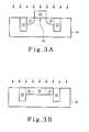
- FIG. 3Arepresents the schematic cross-sectional diagram of power IC whose photo resist layer didn't peel during source implantation
- FIG. 3Brepresents the schematic cross-sectional diagram of power IC whose photo resist layer peeled before or during source implantation.
- FIG. 4shows the process flow of the method of power IC inspection in accordance with the present invention.
- FIG. 5is an optical microscope diagram of power IC inspection for a substrate containing normal power ICs and electrically-failed power ICs according to the method of the present invention.
- the present inventionrelates to a method of power IC inspection, more particularly, to a method applied to inspect whether the electrically-failed power ICs results from photo resist peeling before or during source implantation.
- the present inventionis applicable when the electronically-inspection yield of power ICs significantly decreases. For the electrically failed power ICs, there are lots of reasons to make them fail.
- the present inventionprovide a method to verify whether the decrease of yield results from photo resist peeling during photolithography process before source implantation.
- FIG. 3Arepresents the schematic cross-sectional diagram of power IC whose photo resist layer didn't peel before source implantation
- FIG. 3Brepresents the schematic cross-sectional diagram of power IC whose photo resist layer peeled before source implantation.
- the power ICis manufactured in a semiconductor substrate 10 .
- the gate electrode 12 of the power ICis formed in a deep trench by performing a series of conventional photolithography process, anisotropic etching step and chemical vapor deposition process.
- the source 14 of the power ICis manufactured by first coating a photo resist layer 16 on the semiconductor substrate 10 . After defining the position of source 14 by performing a photolithography process, the source 14 of the power IC is formed by ion-implanting N-type impurities into the semiconductor substrate 10 . Because the photo resist layer 16 serves as hard mask during the ion implantation process, the undoped region 18 between source and drain is not ion-implanted.
- FIG. 3Bshows schematic cross-sectional diagram of the electrically-failed power IC. Because the photo resist layer 16 peeled before or during the ion implantation step for forming source 14 , the undoped region 18 inside the source is also ion-implanted during source implantation. As a result, the breakdown voltage of source 14 to drain 20 is too poor to well work.
- step 101the hot spots on the semiconductor substrate 10 are discovered by performing liquid crystal experiment.
- step 102each power ICs manufactured on the semiconductor substrate 10 is laser-marked according to the hot spots.
- the metal layers on the power ICsare removed by the conventional etching process (step 103 ), and then the dielectric layers on the power ICs are also removed by the conventional etching process (step 104 ).
- the semiconductor substrate 10is put into an acid solution containing chromium (Cr) (step 105 ), so that a close contour is shown at each of the power ICs whose photo resist didn't peel before and after source implantation.
- the close contourcould be a round-shaped contour or an elliptical contour, depending on the layout of the power ICs.
- no contouris shown at the power ICs whose photo resist peeled before or after source implantation.
- the semiconductor substrate 10is first input into a solution composed of HNO 3 /CH 3 COOH/H 3 PO 4 /H 2 O under a temperature ranged between 40 to 45° C. until bubbles are no more generated.
- the HNO 3 /CH 3 COOH/H 3 PO 4 /H 2 O solutionhas a composition ratio of 1:1:17:1.
- the semiconductor substrate 10is then rinsed by using DI water.
- the semiconductor substrate 10is input into a solution composed of HCl/H 2 O 2 /H 2 O for 1 to 3 minutes, and then rinsed by using DI water.
- the HCl/H 2 O 2 /H 2 O solutionhas a composition ratio of 1:5:3.
- the semiconductor substrate 10is input into a solution composed of H 2 SO 4 /H 2 O for 1 to 3 minutes, and then rinsed by using DI water.
- the H 2 SO 4 /H 2 O solutionhas a composition ratio of 1:1.
- the recipe mentioned abovecan be replaced by other acid solutions, such as 5% dilute HF solution, HNO 3 solution accompanied by supersonic vibration, HCl/H 2 O 2 solution with 1:1 ratio accompanied by supersonic vibration, H 2 SO 4 /H 2 O 2 solution with 1:1 ratio accompanied by supersonic vibration, and so on.
- acid solutionssuch as 5% dilute HF solution, HNO 3 solution accompanied by supersonic vibration, HCl/H 2 O 2 solution with 1:1 ratio accompanied by supersonic vibration, H 2 SO 4 /H 2 O 2 solution with 1:1 ratio accompanied by supersonic vibration, and so on.
- the semiconductor substrate 10is first input into a HF/H 2 O solution with a composition ratio of 1:9 for 12 to 20 minutes.
- the semiconductor substrate 10is first input into a HF/H 2 O solution with a composition ratio of 1:9 for 16 minutes.
- the semiconductor substrate 10is then rinsed by using DI water.
- the acid solution containing chromium (Cr)is HNO 3 /HF/CrO 3 /H 2 O solution.
- the HNO 3 /HF/CrO 3 /H 2 O solutionis prepared by first dissolving 50 grams of CrO 3 into 400 ml of water, and then inputting 96% of 100 ml of CrO 3 and 49% of 300 ml of HF into said water.
- the semiconductor substrate 10is input into the HNO 3 /HF/CrO 3 /H 2 O solution for 10 to 20 seconds.
- the semiconductor substrate 10is input into the HNO 3 /HF/CrO 3 /H 2 O solution for 15 seconds.
- HNO 3is applied to oxidize the semiconductor substrate to form a layer of silicon dioxide, and HF is then applied to remove the layer of silicon dioxide.
- CrO 3is the most important one, whose etching rate for etching N-doped silicon substrate is slower than that for etching P-doped silicon substrate.
- the undoped region 18 within P-wellkeeps P-type, because the photo resist layer 16 serves as hard mask during source implantation.
- FIG. 5is an optical microscope diagram of power IC inspection for a substrate containing normal power ICs and electrically-failed power ICs according to the method of the present invention.
- the undoped region 18 within P-wellbecomes N-type during source implantation because the photo resist layer peeled before or during source implantation.
- the etching rate of HNO 3 /HF/CrO 3 /H 2 O solution for etching source 14is the same as that for etching the undoped region 18 .
- each of the electrically-failed power ICsemerges no close contour after dipping into the HNO 3 /HF/CrO 3 /H 2 O solution, as shown by the array 200 in FIG. 5 .
- the present inventionprovides a method of power IC inspection to inspect whether a electrically-failed portion of the power ICs results from photo resist peeling during photolithography process before or during source implantation process.
Landscapes
- Engineering & Computer Science (AREA)
- Manufacturing & Machinery (AREA)
- Computer Hardware Design (AREA)
- Microelectronics & Electronic Packaging (AREA)
- Power Engineering (AREA)
- Testing Or Measuring Of Semiconductors Or The Like (AREA)
Abstract
Description
1. Field of the Invention
The present invention relates to a method of power IC inspection, more particularly, to a method applied to inspect whether electrically-failed power ICs results from photo resist peeling before or during source implantation.
2. Description of the Related Art
Vigorous developments of power ICs are now under way. First refer to FIG.1 and FIG. 2, which represent the schematic cross-sectional diagram and top-view diagram of power ICs, respectively. The power IC is formed on asemiconductor substrate 10. Thegate 12 of the power IC is formed in a deep trench by performing a series of conventional photolithography, anisotropic etching step, and chemical vapor deposition. Thesource 14 of thepower IC 14 is formed by first coating aphoto resist layer 16, defining the region ofsource 14 by photolithography process, and then ion-implanting N-impurities (for NMOS) or P-impurities (for PMOS) into thesemiconductor substrate 10. Theundoped region 18 between source and drain is not ion-implanted because thephoto resist layer 16 serves as a hard mask during source implantation.
However, thephoto resist layer 16 might peel during the photolithography process. As a result, theundoped region 18 is ion-implanted during source implantation because of no hard mask. As a result, the breakdown voltage ofsource 14 to drain20 is too poor to well work.
In order to avoid from ion-implanting in error, it would be the best to inspect thephoto resist layer 16 before or after source implantation. In the present semiconductor industry, only optical scanners of KLA-Tencor can inspect the pattern of thephoto resist layer 16 automatically. However, the optical scanners of KLA-Tencor are with very low throughput. For this reason, only few semiconductor substrates can be sampled in the real application. As a result, some of electrically-failed power ICs resulted from photo resist peeling will be released from inspection until final electrical test.
There are lots of potential reasons resulting in the failure of the electrically-failed power ICs. In the present, there is no method which can verify whether the failure of the electrically-failed power ICs results from photo resist peeling. This issue embarrasses both of the QC (Quality Control) people and the process people.
The main purpose of the present invention is to provide a method of power IC inspection to inspect whether a electrically-failed portion of power ICs results from photo resist peeling during photolithography process during source implantation process.
The present invention provides a method of power IC inspection to inspect whether electrically-failed power ICs results from photo resist peeling during source implantation. First, the hot spots on thesemiconductor substrate 10 are recovered by performing liquid crystal experiment. After that, each of the electrically-failed power ICs manufactured on thesemiconductor substrate 10 is laser-marked according to the hot spots.
Thereafter, the metal layers on the power ICs are removed by the conventional etching process, and then the dielectric layers on the power ICs are also removed by the conventional etching process. Finally, thesemiconductor substrate 10 is put into an acid solution containing chromium (Cr), so that a close contour is shown at each of the power ICs whose photo resist layer didn't peel during photolithography process during source implantation process.
The acid solution containing chromium (Cr) is HNO3/HF/CrO3/H2O solution. The HNO3/HF/CrO3/H2O solution is prepared by first dissolving 50 grams of CrO3solution into 400 ml of water, and then inputting 96% of 100 ml of CrO3solution and 49% of 300 ml of HF into the water. According to one embodiment of the present invention, thesemiconductor substrate 10 is input into the HNO3/HF/CrO3/H2O solution for 10 to 20 seconds. According to another embodiment of the present invention, thesemiconductor substrate 10 is input into the HNO3/HF/CrO3/H2O solution for 15 seconds.
FIG. 1 represent the conventional cross-sectional diagram of power ICs.
FIG. 2 represent the conventional top-view diagram of power ICs.
FIG. 3A represents the schematic cross-sectional diagram of power IC whose photo resist layer didn't peel during source implantation;
FIG. 3B represents the schematic cross-sectional diagram of power IC whose photo resist layer peeled before or during source implantation.
FIG. 4 shows the process flow of the method of power IC inspection in accordance with the present invention.
FIG. 5 is an optical microscope diagram of power IC inspection for a substrate containing normal power ICs and electrically-failed power ICs according to the method of the present invention.
The present invention relates to a method of power IC inspection, more particularly, to a method applied to inspect whether the electrically-failed power ICs results from photo resist peeling before or during source implantation. The present invention is applicable when the electronically-inspection yield of power ICs significantly decreases. For the electrically failed power ICs, there are lots of reasons to make them fail. The present invention provide a method to verify whether the decrease of yield results from photo resist peeling during photolithography process before source implantation.
Referring first to FIG. 3, the schematic cross-sectional diagram of power ICs is shown. FIG. 3A represents the schematic cross-sectional diagram of power IC whose photo resist layer didn't peel before source implantation; FIG. 3B represents the schematic cross-sectional diagram of power IC whose photo resist layer peeled before source implantation.
In FIG. 3A, the power IC is manufactured in asemiconductor substrate 10. Thegate electrode 12 of the power IC is formed in a deep trench by performing a series of conventional photolithography process, anisotropic etching step and chemical vapor deposition process. Thesource 14 of the power IC is manufactured by first coating aphoto resist layer 16 on thesemiconductor substrate 10. After defining the position ofsource 14 by performing a photolithography process, thesource 14 of the power IC is formed by ion-implanting N-type impurities into thesemiconductor substrate 10. Because thephoto resist layer 16 serves as hard mask during the ion implantation process, theundoped region 18 between source and drain is not ion-implanted.
On the other hand, FIG. 3B shows schematic cross-sectional diagram of the electrically-failed power IC. Because thephoto resist layer 16 peeled before or during the ion implantation step for formingsource 14, theundoped region 18 inside the source is also ion-implanted during source implantation. As a result, the breakdown voltage ofsource 14 to drain20 is too poor to well work.
Referring now to FIG. 4, the process flow of the method of power IC inspection is shown. First, the hot spots on thesemiconductor substrate 10 are discovered by performing liquid crystal experiment (step101). After that, each power ICs manufactured on thesemiconductor substrate 10 is laser-marked according to the hot spots (step102).
Thereafter, the metal layers on the power ICs are removed by the conventional etching process (step103), and then the dielectric layers on the power ICs are also removed by the conventional etching process (step104). Finally, thesemiconductor substrate 10 is put into an acid solution containing chromium (Cr) (step105), so that a close contour is shown at each of the power ICs whose photo resist didn't peel before and after source implantation. The close contour could be a round-shaped contour or an elliptical contour, depending on the layout of the power ICs. On the other hand, no contour is shown at the power ICs whose photo resist peeled before or after source implantation.
About the step of removing the metal layers on the power ICs, thesemiconductor substrate 10 is first input into a solution composed of HNO3/CH3COOH/H3PO4/H2O under a temperature ranged between 40 to 45° C. until bubbles are no more generated. The HNO3/CH3COOH/H3PO4/H2O solution has a composition ratio of 1:1:17:1. Thesemiconductor substrate 10 is then rinsed by using DI water. After that, thesemiconductor substrate 10 is input into a solution composed of HCl/H2O2/H2O for 1 to 3 minutes, and then rinsed by using DI water. The HCl/H2O2/H2O solution has a composition ratio of 1:5:3. Thereafter, thesemiconductor substrate 10 is input into a solution composed of H2SO4/H2O for 1 to 3 minutes, and then rinsed by using DI water. The H2SO4/H2O solution has a composition ratio of 1:1.
According to another embodiments of the present invention, the recipe mentioned above can be replaced by other acid solutions, such as 5% dilute HF solution, HNO3solution accompanied by supersonic vibration, HCl/H2O2solution with 1:1 ratio accompanied by supersonic vibration, H2SO4/H2O2solution with 1:1 ratio accompanied by supersonic vibration, and so on.
About the step of removing the dielectric layers on the power ICs, thesemiconductor substrate 10 is first input into a HF/H2O solution with a composition ratio of 1:9 for 12 to 20 minutes. According to another embodiment of the present invention, thesemiconductor substrate 10 is first input into a HF/H2O solution with a composition ratio of 1:9 for 16 minutes. Thesemiconductor substrate 10 is then rinsed by using DI water.
The acid solution containing chromium (Cr) is HNO3/HF/CrO3/H2O solution. The HNO3/HF/CrO3/H2O solution is prepared by first dissolving 50 grams of CrO3into 400 ml of water, and then inputting 96% of 100 ml of CrO3and 49% of 300 ml of HF into said water. According to one embodiment of the present invention, thesemiconductor substrate 10 is input into the HNO3/HF/CrO3/H2O solution for 10 to 20 seconds. According to another embodiment of the present invention, thesemiconductor substrate 10 is input into the HNO3/HF/CrO3/H2O solution for 15 seconds.
Within the HNO3/HF/CrO3/H2O solution, HNO3is applied to oxidize the semiconductor substrate to form a layer of silicon dioxide, and HF is then applied to remove the layer of silicon dioxide. CrO3is the most important one, whose etching rate for etching N-doped silicon substrate is slower than that for etching P-doped silicon substrate. For the normal power IC represented in FIG. 3A, theundoped region 18 within P-well keeps P-type, because the photo resistlayer 16 serves as hard mask during source implantation. Becausesource 14 is N-type, the etching rate of HNO3/HF/CrO3/H2O solution for etchingsource 14 is slower than that for etching theundoped region 18. For this reason, each of the normal power ICs emerges a close contour after dipping into the HNO3/HF/CrO3/H2O solution, as shown by thearray 100 in FIG.5. FIG. 5 is an optical microscope diagram of power IC inspection for a substrate containing normal power ICs and electrically-failed power ICs according to the method of the present invention.
On the other hand, for the electrically-failed power ICs represented in FIG. 3B, theundoped region 18 within P-well becomes N-type during source implantation because the photo resist layer peeled before or during source implantation. As a result, the etching rate of HNO3/HF/CrO3/H2O solution for etchingsource 14 is the same as that for etching theundoped region 18. For this reason, each of the electrically-failed power ICs emerges no close contour after dipping into the HNO3/HF/CrO3/H2O solution, as shown by thearray 200 in FIG.5.
According to the reasons mentioned above, the present invention provides a method of power IC inspection to inspect whether a electrically-failed portion of the power ICs results from photo resist peeling during photolithography process before or during source implantation process.
It should be understood that the foregoing relates to only preferred embodiments of the present invention, and that it is intended to cover all changes and modifications of the embodiments of the invention herein used for the purposes of the disclosure, which do not constitute departures from the spirit and scope of the invention.
Claims (22)
1. A method of power IC inspection for a number of power ICs manufactured on a semiconductor substrate, wherein said method is applied to inspect whether an electrically-failed portion of said power ICs results from photo resist peeling before or during source implantation, comprising:
a. removing metal layers on said power ICs;
b. removing dielectric layers on said power ICs; and
c. putting said semiconductor substrate into an acid solution containing chromium (Cr); whereby a close contour is shown at each of said power ICs whose photoresist did not peel before and during source implantation.
2. The method ofclaim 1 , wherein said acid solution is HNO3/HF/CrO3/H2O solution.
3. The method ofclaim 1 , wherein said HNO3/HF/CrO3/H2O solution is prepared by first dissolving 50 grams of CrO3into 400 ml of water, and then inputting 96% of 100 ml of CrO3and 49% of 300 ml of HF into said water.
4. The method ofclaim 1 , before said step of removing metal layers on said power ICs further comprising:
recovering hot spots on said semiconductor substrate by performing liquid crystal experiment; and
laser-marking each of said electrically-failed portion of said power ICs according to said hot spots.
5. The method ofclaim 1 , wherein said close contour is a round-shaped contour.
6. The method ofclaim 1 , wherein said close contour depends on the photolithography process.
7. The method ofclaim 1 , wherein said step of removing metal layers on said power ICs comprises:
a. inputting said semiconductor substrate into a solution composed of HNO3/CH3COOH/H3PO4/H2O under a temperature ranged between 40 to 45° C. until bubbles are no more generated; and then rinsing said semiconductor substrate by using DI water;
b. inputting said semiconductor substrate into a solution composed of HCl/H2O2/H2O for 1 to 3 minutes, and then rinsing said semiconductor substrate by using DI water;
c. inputting said semiconductor substrate into a solution composed of H2SO4/H2O for 1 to 3 minutes, and then rinsing said semiconductor substrate by using DI water.
8. The method ofclaim 7 , wherein said HNO3/CH3COOH/H3PO4/H2O solution has a composition ratio of 1:1:17:1.
9. The method ofclaim 7 , wherein said HCl/H2O2/H2O solution has a composition ratio of 1:5:3.
10. The method ofclaim 7 , wherein said H2SO4/H2O solution has a composition ratio of 1:1.
11. The method ofclaim 1 , wherein said step of removing dielectric layers on said power ICs is composed of inputting said semiconductor substrate into a HF/H2O solution for 12 to 20 minutes, and then rinsing said semiconductor substrate by using DI water.
12. The method ofclaim 11 , wherein said HF/H2O solution has a composition ratio of 1:9.
13. A method of power IC inspection for a number of power ICs manufactured on a semiconductor substrate, wherein said method is applied to inspect whether an electrically-failed portion of said power ICs results from photo resist peeling before or during source implantation, comprising:
a. discovering hot spots on said semiconductor substrate by performing liquid crystal experiment and then laser-marking each of said electrically-failed portion of said power ICs according to said hot spots;
b. removing metal layers on said power ICs;
c. removing dielectric layers on said power ICs;
d. putting said semiconductor substrate into a HNO3/HF/CrO3/H2O solution;
whereby a close contour is shown at each of said power ICs whose photoresist did not peel during photolithography process before and during source implantation, and no contour is shown at each of said power ICs whose photoresist peeled before or during source implantation.
14. The method ofclaim 13 , wherein said HNO3/HF/CrO3/H2O solution is prepared by first dissolving 50 grams of CrO3into 400 ml of water, and then inputting 96% of 100 ml of CrO3and 49% of 300 ml of HF into said water.
15. The method ofclaim 13 , wherein said close contour is with the shape defined by the photolithography process.
16. The method ofclaim 13 , wherein said close contour is an elliptical contour.
17. The method ofclaim 13 , wherein said step of removing metal layers on said power ICs comprises:
a. inputting said semiconductor substrate into a solution composed of HNO3/CH3COOH/H3PO4/H2O under a temperature ranged between 40 to 45° C. until bubbles are no more generated; and then rinsing said semiconductor substrate by using DI water;
b. inputting said semiconductor substrate into a solution composed of HCl/H2O2/H2O for 1 to 3 minutes, and then rinsing said semiconductor substrate by using DI water;
c. inputting said semiconductor substrate into a solution composed of H2SO4/H2O for 1 to 3 minutes, and then rinsing said semiconductor substrate by using DI water.
18. The method ofclaim 17 , wherein said HNO3/CH3COOH/H3PO4/H2O solution has a composition ratio of 1:1:17:1.
19. The method ofclaim 17 , wherein said HCl/H2O2/H2O solution has a composition ratio of 1:5:3.
20. The method ofclaim 17 , wherein said H2SO4/H2O solution has a composition ratio of 1:1.
21. The method ofclaim 13 , wherein said step of removing dielectric layers on said power ICs is composed of inputting said semiconductor substrate into a HF/H2O solution for 12 to 20 minutes, and then rinsing said semiconductor substrate by using DI water.
22. The method ofclaim 21 , wherein said HF/H2O solution has a composition ratio of 1:9.
Applications Claiming Priority (3)
| Application Number | Priority Date | Filing Date | Title |
|---|---|---|---|
| TW8912356A | 2000-11-03 | ||
| TW089123256ATW463283B (en) | 2000-11-03 | 2000-11-03 | Inspection method of photolithography process for power transistor processing |
| TW89123256 | 2000-11-03 |
Publications (2)
| Publication Number | Publication Date |
|---|---|
| US20020055196A1 US20020055196A1 (en) | 2002-05-09 |
| US6509198B2true US6509198B2 (en) | 2003-01-21 |
Family
ID=21661798
Family Applications (1)
| Application Number | Title | Priority Date | Filing Date |
|---|---|---|---|
| US09/969,601Expired - LifetimeUS6509198B2 (en) | 2000-11-03 | 2001-10-04 | Method of power IC inspection |
Country Status (2)
| Country | Link |
|---|---|
| US (1) | US6509198B2 (en) |
| TW (1) | TW463283B (en) |
Cited By (1)
| Publication number | Priority date | Publication date | Assignee | Title |
|---|---|---|---|---|
| US20070044710A1 (en)* | 2005-08-31 | 2007-03-01 | Joerg Buschbeck | Technique for monitoring dynamic processes in metal lines of microstructures |
Families Citing this family (1)
| Publication number | Priority date | Publication date | Assignee | Title |
|---|---|---|---|---|
| US20070227700A1 (en)* | 2006-03-29 | 2007-10-04 | Dimitrakopoulos Christos D | VLSI chip hot-spot minimization using nanotubes |
Citations (7)
| Publication number | Priority date | Publication date | Assignee | Title |
|---|---|---|---|---|
| US3868720A (en)* | 1973-12-17 | 1975-02-25 | Westinghouse Electric Corp | High frequency bipolar transistor with integral thermally compensated degenerative feedback resistance |
| US4839311A (en)* | 1987-08-14 | 1989-06-13 | National Semiconductor Corporation | Etch back detection |
| US4846929A (en)* | 1988-07-13 | 1989-07-11 | Ibm Corporation | Wet etching of thermally or chemically cured polyimide |
| US5804980A (en)* | 1994-08-31 | 1998-09-08 | Nec Corporation | Method and system for testing an interconnection in a semiconductor integrated circuit |
| US5872051A (en)* | 1995-08-02 | 1999-02-16 | International Business Machines Corporation | Process for transferring material to semiconductor chip conductive pads using a transfer substrate |
| US6181662B1 (en)* | 1997-09-26 | 2001-01-30 | Iomega Corporation | Latent irradiance discrimination method and marker system for cartridgeless data storage disks |
| US6376374B1 (en)* | 1998-05-12 | 2002-04-23 | Semitool, Inc. | Process and manufacturing tool architecture for use in the manufacturing of one or more protected metallization structures on a workpiece |
- 2000
- 2000-11-03TWTW089123256Apatent/TW463283B/ennot_activeIP Right Cessation
- 2001
- 2001-10-04USUS09/969,601patent/US6509198B2/ennot_activeExpired - Lifetime
Patent Citations (7)
| Publication number | Priority date | Publication date | Assignee | Title |
|---|---|---|---|---|
| US3868720A (en)* | 1973-12-17 | 1975-02-25 | Westinghouse Electric Corp | High frequency bipolar transistor with integral thermally compensated degenerative feedback resistance |
| US4839311A (en)* | 1987-08-14 | 1989-06-13 | National Semiconductor Corporation | Etch back detection |
| US4846929A (en)* | 1988-07-13 | 1989-07-11 | Ibm Corporation | Wet etching of thermally or chemically cured polyimide |
| US5804980A (en)* | 1994-08-31 | 1998-09-08 | Nec Corporation | Method and system for testing an interconnection in a semiconductor integrated circuit |
| US5872051A (en)* | 1995-08-02 | 1999-02-16 | International Business Machines Corporation | Process for transferring material to semiconductor chip conductive pads using a transfer substrate |
| US6181662B1 (en)* | 1997-09-26 | 2001-01-30 | Iomega Corporation | Latent irradiance discrimination method and marker system for cartridgeless data storage disks |
| US6376374B1 (en)* | 1998-05-12 | 2002-04-23 | Semitool, Inc. | Process and manufacturing tool architecture for use in the manufacturing of one or more protected metallization structures on a workpiece |
Cited By (2)
| Publication number | Priority date | Publication date | Assignee | Title |
|---|---|---|---|---|
| US20070044710A1 (en)* | 2005-08-31 | 2007-03-01 | Joerg Buschbeck | Technique for monitoring dynamic processes in metal lines of microstructures |
| US8118932B2 (en)* | 2005-08-31 | 2012-02-21 | Advanced Micro Devices, Inc. | Technique for monitoring dynamic processes in metal lines of microstructures |
Also Published As
| Publication number | Publication date |
|---|---|
| TW463283B (en) | 2001-11-11 |
| US20020055196A1 (en) | 2002-05-09 |
Similar Documents
| Publication | Publication Date | Title |
|---|---|---|
| US20020115284A1 (en) | Method of cleaning a dual damascene structure | |
| US6878646B1 (en) | Method to control critical dimension of a hard masked pattern | |
| US5217911A (en) | Method of producing a semiconductor structure including a Schottky junction | |
| US6461973B1 (en) | Method for forming high quality multiple thickness oxide layers by reducing descum induced defects | |
| US6509198B2 (en) | Method of power IC inspection | |
| US7928000B2 (en) | Method for forming self aligned contacts for integrated circuit devices | |
| US8852673B2 (en) | Defect monitoring for resist layer | |
| US5858861A (en) | Reducing nitride residue by changing the nitride film surface property | |
| US5930650A (en) | Method of etching silicon materials | |
| US6251568B1 (en) | Methods and apparatus for stripping photoresist and polymer layers from a semiconductor stack in a non-corrosive environment | |
| US7727900B2 (en) | Surface preparation for gate oxide formation that avoids chemical oxide formation | |
| US8940641B1 (en) | Methods for fabricating integrated circuits with improved patterning schemes | |
| KR100255665B1 (en) | Method for fabricating semiconductor device which havig a different thickness gate oxide structure in a semiconductor substrate | |
| CN114093813A (en) | Method for manufacturing contact hole for semiconductor device | |
| US6432618B1 (en) | Method for forming high quality multiple thickness oxide layers by reducing descum induced defects | |
| KR100596899B1 (en) | Manufacturing Method of Semiconductor Device | |
| JPH10261627A (en) | Manufacturing method of semiconductor device | |
| KR20000073897A (en) | Cleaning methode for exclusion the poly silicon's defect in process for separate cell by selectivity poly-silicon oxidation | |
| US20240114804A1 (en) | Method for preparing multi-superconducting material layers, quantum device and quantum chip | |
| US7576374B2 (en) | Semiconductor device with robust polysilicon fuse | |
| KR100281270B1 (en) | Contact manufacturing method of semiconductor device | |
| KR100528445B1 (en) | A method of forming dual gate oxide | |
| JPS60233824A (en) | Treating method for semiconductor substrate | |
| KR100235959B1 (en) | Process for forming metal interconnector in semiconductor device | |
| KR20050068363A (en) | Method for fabricating thin pattern using the hard mask |
Legal Events
| Date | Code | Title | Description |
|---|---|---|---|
| AS | Assignment | Owner name:MOSEL VITELIC INC., TAIWAN Free format text:ASSIGNMENT OF ASSIGNORS INTEREST;ASSIGNORS:JAW, KOU-LIANG;CHEN, JEN-TE;REEL/FRAME:012231/0319 Effective date:20010905 | |
| FEPP | Fee payment procedure | Free format text:PAYOR NUMBER ASSIGNED (ORIGINAL EVENT CODE: ASPN); ENTITY STATUS OF PATENT OWNER: LARGE ENTITY | |
| STCF | Information on status: patent grant | Free format text:PATENTED CASE | |
| AS | Assignment | Owner name:PROMOS TECHNOLOGIES INC., TAIWAN Free format text:ASSIGNMENT OF ASSIGNORS INTEREST;ASSIGNOR:MOSEL VITELIC, INC.;REEL/FRAME:015334/0772 Effective date:20040427 | |
| FPAY | Fee payment | Year of fee payment:4 | |
| REMI | Maintenance fee reminder mailed | ||
| FPAY | Fee payment | Year of fee payment:8 | |
| SULP | Surcharge for late payment | Year of fee payment:7 | |
| FPAY | Fee payment | Year of fee payment:12 |