US6507941B1 - Subgrid detailed routing - Google Patents
Subgrid detailed routingDownload PDFInfo
- Publication number
- US6507941B1 US6507941B1US09/301,143US30114399AUS6507941B1US 6507941 B1US6507941 B1US 6507941B1US 30114399 AUS30114399 AUS 30114399AUS 6507941 B1US6507941 B1US 6507941B1
- Authority
- US
- United States
- Prior art keywords
- grid
- subgrid
- indicia
- representation
- subgrids
- Prior art date
- Legal status (The legal status is an assumption and is not a legal conclusion. Google has not performed a legal analysis and makes no representation as to the accuracy of the status listed.)
- Expired - Lifetime
Links
Images


Classifications
- G—PHYSICS
- G06—COMPUTING OR CALCULATING; COUNTING
- G06F—ELECTRIC DIGITAL DATA PROCESSING
- G06F30/00—Computer-aided design [CAD]
- G06F30/30—Circuit design
- G06F30/39—Circuit design at the physical level
- G06F30/394—Routing
Definitions
- the present inventionrelates to a router for use in fabricating integrated circuit chips, and, more specifically, a subgrid detailed router
- routingis the term used describe placing wires into locations on an integrated circuit chip.
- the overall design flow of the physical designincludes receiving a cell level netlist, as shown in step 2 . Thereafter, this cell level netlist is used to determine the placement of modules that exist within the netlist into locations on the chip, shown as step 4 .
- Moduleswill contain information relating to a combination of logical functions, and will include the pin and obstacle information needed for routing purposes.
- the netlistwill also contain information relating to the various different pins that need to be interconnected.
- a global routing grid(which may have been implemented in the placement step), is used to route various wires between pins of modules that traverse paths over several global routing grids.
- a detailed routing grid(or simply routing grid hereafter) is implemented, typically at a higher resolution than the previously discussed global routing grid, and the detailed placement of wires is performed.
- the output of the detailed routing step 8is an integrated circuit fabrication mask.
- each of the different layers of an integrated circuit chipis represented in the detailed routing grid.
- the detailed routing gridis a 3D representation, with each of the different layers of the integrated circuit needed for routing purposes having a uniform area that is subdivided into the routing grids previously discussed, thereby forming a grid pattern for each layer.
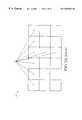
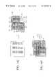
- FIG. 2Aillustrates one layer of such a 3D routing grid, in which that layer is subdivided into a grid pattern 10 having separate grids 12 of uniform size.
- This uniform size of the grids 12is typically determined by the minimum width of the wires that can be obtained plus the minimum spacing that must be maintained between adjacent wires and/or vias.
- the 3D routing gridwill have layers corresponding to the different routing layers.
- a typical integrated circuitwill have at least a semiconductor layer, and three wiring layers, such as HVH wiring layers, which stands for horizontal, vertical and horizontal wiring.
- HVH wiringone wiring layer (H 1 ) is generally used to make horizontal traversals
- another wiring layer (V)is generally used to make vertical traversals
- another layer (H 2 )is generally used to make horizontal traversals.
- the detailed routerWhen performing detailed routing, the detailed router receives chip technology description data and data that has been generated as a result of the global routing step, which describe data including the number of layers (levels) on which rectangles representing wires can be generated, the minimum allowed width of any part of the path of rectangles, and the minimum allowed separation between any non-electrically-connected rectangles, as is conventionally known.
- the centerline conventionis that the grid describes the acceptable location for the centerline of the paths that is used during the expansion process to determine the path of a net.
- the pathmust stay away from existing obstacles, such as other wires, vias, and pins of other nets that have been previously placed in the 3D routing grid.
- theyare modeled by marking certain grid points as invalid.
- every intersection of the horizontal and vertical equidistant gridlinesis tracked as a position to which the center of a square of a net to be routed may be assigned when legal. Such an assignment is legal if the square centered on the grid point has legal separation with respect to all other rectangles not associated with the net currently being routed. It may require traversals over several proposed paths before a successful traversal results in a placement location being found
- FIG. 3illustrates a representation of a portion of a routing grid and the obstacles and pins associated therewith.
- pins 12 A and 12 bassociated with one module are pins 12 A and 12 b , and obstacles 14 A and 14 B.
- Associated with another moduleare Pins 12 C and 12 D; and obstacles 14 C and 14 D.
- the region marked 14 Eshows the interconnection of the pins 12 B and 12 C. Thus, for interconnections of other nets, the region marked 14 E will also be an obstacle.
- the detailed routerUsing a list of the different pins that need to be connected, the detailed router will traverse a path from the initial pin location (such as pin 12 B in FIG. 3, to an endpoint pin location (such as pin 12 C In reply to FIG. 3 ). It should be noted that in many cases, there exist many different possible connection locations to which the endpoint pin location can legally go, and once the detailed router finds a first such endpoint pin location, it has completed its task for that net, and will then move onto routing the next net. It should be noted that provision is also made for routing vias that connect conductors that exist at different adjacent levels and are used to form a single wire.
- obstacle and wire congestion modeling analysesare also used in grid based routing systems to increase the likelihood that the particular wire placement determined during the global routing stage can actually be implemented at a finer level (i.e., within a portion of the grid in which it was placed).
- these modeling techniquesare either too optimistic at the expense of routing completion or too pessimistic at the expense of density.
- conventional grid based routing systemsare not able to implement all of the design requirements.
- the choice of the routing gridis extremely important, as it affects the packing efficiency, which measures how tightly the wires can be packed, with the constraint that the centerlines of the wires are on the chosen grid, compared to the packing in a gridless world.
- the width and spacingare both 0.4 ⁇ m (0.4 microns) on all layers, as illustrated in FIGS. 4A and 4B.
- a natural routing gridhas track separations of 0.8 ⁇ m (both horizontally and vertically) as illustrated in FIG. 4C, and adjacent wires can be packed at 100% packing efficiency.
- the routing gridis chosen to be 0.6 ⁇ m or 1.2 ⁇ m, as illustrated in FIGS. 4D and 4E, then the wires can only be packed at 66% packing efficiency.
- the routing gridis chosen to be 0.4 ⁇ m, the wires can be maximally packed at 100%, but the size of the grid is quadrupled (doubled in each direction).
- a gridless routing systemThe other approach that has been used for routing is known as a gridless routing system.
- gridlesssuch routing does not use a grid for routing, but instead keeps track of all of the obstacles based upon their location with respect to each other.
- Such a gridless routing systemtheoretically has as an advantage in that it can find a path that does not have to adhere to a predefined routing grid, as in the case of a grid-based router. While this theoretical advantage exists, such systems are technically complex and complicated, do not typically perform as well as expected, and are typically slow, especially as the integrated circuit that is being routed becomes more and more complex.
- the present inventionattains the above-recited objects of the present invention, among others, by implementing a detailed subgrid router that performs searches for wire locations at the grid level. Once a solution is found, the wire representation is made based upon a finer subgrid. Due to the manner in which the search is performed at the grid level, the present invention guarantees that a path for that wire will exist at the finer subgrid level. The rectangles representing the wire is then stored in the database that includes the other corresponding information, so that it can be treated as an obstacle when routing a subsequent wire. Specifically, the present invention includes subgrids that in a preferred embodiment have a resolution that is 16X greater than the resolution of the conventional grids. This increased resolution is useful for improving routing density with variable width and variable spacing designs.
- the subgrid detailed router of the present inventionsearches at the grid level for potential wire paths using a code associated with each grid.
- This codecontains data corresponding to each of the subgrids, such that upon completion of a routing a net, information exists that allows for the placement of the net at locations corresponding to the subgrid that has finer resolution than the grid which was used to implement the routing search.
- the present inventionis as efficient as conventional grid based routers in finding an appropriate path.
- FIG. 1illustrates an overview of a conventional place and route process used in the physical design for the fabrication of integrated circuit chips
- FIG. 2Aillustrates a conventional grid used in on layer of a conventional 3D grid-based routing system
- FIG. 2Billustrates representations different physical layers corresponding to the layers of a conventional 3D grid-based routing system
- FIG. 3illustrates a top view of the representation of the pins, obstacles and wires used in a conventional routing system
- FIGS. 4A-4Eillustrate the property of grid selection, packing efficiency and fragmentation
- FIG. 5illustrates a conventional grid used in a conventional grid-based routing system that has 16 times the resolution of the grid illustrated in FIG. 1 ′
- FIG. 6illustrates a block diagram of the subgrid-detailed router according to the present invention
- FIGS. 7 and 8each illustrate different aspects of subgrids according to the present invention.
- FIGS. 9A-9Cillustrate the process of conventional grid based routing
- FIGS. 10A-10Cillustrate the process of subgrid detailed routing according to the present invention
- FIGS. 11A-11B and 12 A- 12 Billustrate different manners of abstracting wire widths and spacing in a grid based routing system
- FIGS. 13A-13Billustrate a manner of abstracting wire widths and spacing in the subgrid detailed router according to the present invention
- FIGS. 14A-14Fillustrate the an aspect of the data representation process according to the subgrid detailed routing according to the present invention
- FIGS. 15A-15Fillustrate examples of grids that satisfy the single component assumption according to the present invention.
- FIGS. 16A-16Fillustrate examples of grids that do not satisfy the single component assumption according to the present invention.
- FIG. 17illustrates the process of altering a grid that does not satisfy the single component assumption into a grid that satisfies the single component assumption according to the present invention
- FIGS. 18A-Billustrates a flowchart of the process of the subgrid-detailed router according to a preferred embodiment of the present invention.
- FIG. 19illustrates the process of determining whether a path can be extended from one grid to an adjacent second grid by performing a bitwise AND operation between adjacent subgrids of the two said grids.
- the present inventionimplements a routing approach that handles variable widths and spacing in a simple, intuitive manner.
- the present inventionis implemented in a computer system, such as an Intel processor based computer system running on a Unix operating system platform.
- the present inventionis implemented as a sequence of coded program instructions, preferably written in an object oriented programming language such as C++.
- the present inventionis run as a router application program, described in detail hereinafter, that accepts data corresponding to the desired characteristics of the integrated circuit chip, typically known as a netlist that represents the nets, modules, and pins as described previously, and operates upon this data to determine the placement of wires in an integrated circuit chip representation, thereby resulting in routing data that is output from the router.
- the router 20is grid based, and for a bounded area 10 has grids 12 that have similarities to that of conventional grid based routing system. While the placement of modules be performed along with as in a conventional grid-based routing system, placement of modules can also be performed using a timing driven approach such as described in U.S. patent application Ser. No. 09/054,379 entitled Timing Closure Methodology filed on Apr. 2, 1998 in the U.S. Patent and Trademark Office, the contents of which are expressly incorporated by reference herein. Further, the routing of wires can also be incorporated with the routing system described in U.S. patent application Ser. No. 09/054,319 entitled Method of Designing a Constraint Driven Integrated Circuit Layout filed on Apr. 2, 1998 in the U.S. Patent and Trademark Office, the contents of which are expressly incorporated by reference herein.
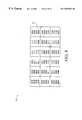
- the present inventionincludes the concept of sub-grids, illustrated as fine grids or sub-grids 22 .
- subgrids 22there are a plurality of subgrids, illustrated in FIG. 7 as subgrids 22 in positions 0 , 1 , 2 , 3 , 4 , 5 , 6 , 7 , 8 , 9 , A, B, C, D, E, and F.
- FIG. 8illustrates the subgrids 22 with the indicia that is associated with each subgrid and used to determine available locations in which to route a wire as will be explained in further detail hereinafter.
- a particular subgridwill have attributed to it an availability indicia in the preferred embodiment as a binary “1”, and a non-availability indicia in the preferred embodiment as a binary “0”.
- this indiciais used to store representations of locations that are available or not for a wire to be placed. Indicia corresponding to the locations that a new wire is routed on will then change from a “1” to a “0” after that new wire is routed.
- the present inventionassociates groups of these indicia together, such that there exists one code for each different grid. Accordingly, by using this code, the present invention is able to have the path finding algorithm, such as the Lee-type algorithm or BFS algorithm, use the grid as the search space when expanding from one grid to another in an attempt to find a legal set of locations that can be used to create a path, but is then able to place the wire, using the determined path, in a solution space that has locations based upon the subgrid.
- the path finding algorithmsuch as the Lee-type algorithm or BFS algorithm
- the subgrid detailed routerperforms searches for wire locations at the grid level, but once a solution is found, the wires are placed in locations on a subgrid level.
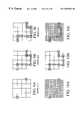
- FIG. 9Aillustrates a conventional routing grid and two pins that need to be connected.
- FIG. 10Aillustrates the subgrid detailed router according to the present invention. It is noted that the resolution of the subgrids is 16X greater according to the present invention than the resolution of the conventional grids. This increased resolution, as will be described in further detail hereinafter, is useful for improving routing density with variable width and variable spacing designs.
- FIG. 9Billustrates routing a net at the coarse level along the grid using a conventional router.
- FIG. 10Billustrates routing a net at the coarse level along the grid using the subgrid-detailed router of according to the present invention.
- both routersroute at the same grid level.
- the primary differenceis that whereas the conventional router searches based upon a single binary representation associated with each grid location, that the present invention searches using the code associated with each grid, as mentioned above.
- the use of searching using this code, rather than using the single binary representation,has extremely minimal impact on the overall runtime of the search.
- the present inventionis as efficient as conventional grid based routers in finding an appropriate path.
- FIG. 9Cillustrates the result of the conventionally routed wire
- FIG. 10Cillustrates the result of the wire routed using the subgrid-detailed router according to the present invention.
- the wire formed using the subgrid-detailed routerhas boundaries determined by the resolution of the subgrids
- the wire formed conventionallyhas boundaries determined by the resolution of the grid.
- the resultant wire spacing that can be accommodated according to the present inventiontherefore, is more precise. It is this precision that allows the present invention to accommodate variable width and variable spacing designs.
- the preferred resolution of the subgrids 22is 16 times that of the grid, in a 4 ⁇ 4 array within the subgrid. While lesser or greater resolutions, such as a 2 ⁇ 2, 3 ⁇ 3, 4 ⁇ 6, 5 ⁇ 5 , 2 ⁇ 8, 8 ⁇ 8 or other arrays for the subgrid 22 are within the intended scope of the present invention, it has been determined that a 4 ⁇ 4 array subgrid 22 provides sufficiently fine resolution to implement circuit designs have advanced design requirements such as variable width and spacing, without overly increasing the complexity of the design, as well as the time that the implemented design takes to operate when being used.
- each subgridforms part of a row or column of subgrids. While each row or column does not need to be the same size, each of the subgrids within each row or column must have dimensions that conform to the dimensions of the row or column.
- reference point routingAs mentioned in the background section, in the centerline convention, the grid describes the acceptable location for the centerline of paths. Reference point routing, such as reference point routing using the centerline convention, is used so that the routing problem can be abstracted to a graph-theoretical problem of finding a least-cost path in a routing graph.
- This graphcan be represented explicitly as a general graph, or implicitly as a 3D array of grid points with certain connectivity information between adjacent grid points. In either case, this abstraction transforms the problem of routing wires with nonzero width and nonzero spacing, into a point-to-point connection problem abstracting away the concept of width and spacing. This will be appreciated from the specific illustration provided below with respect to FIGS. 11A-B, 12 A-B and 13 A-B.
- routing a wire with width W and spacing Sis equivalent to routing a wire with zero width and spacing W/2+S.
- a routing pathis represented by a sequence of “moves” of the reference point between adjacent grids. Each point in the path defines a square of width W with a certain offset with respect to the point.
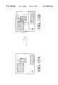
- FIGS 11 A and 11 Billustrates routing a net with width W and spacing S
- Such a representationcan, as noted above, be translated to routing a net with width 0 and spacing W/2+S, as illustrated in FIGS. 12A and 12B.
- the path found using the latter approach of FIGS. 12A-12Bis equivalent to the centerline of the path found using the first approach of FIGS. 11A-11B.
- FIGS. 12A-12Bcan be transformed to a third approach, illustrated in FIGS. 13A and 13B.
- each obstacle Ris bloated by W/2+S, and xl, xr, yb, yt are set as the coordinates of R.
- the bloating of R by B(a positive value) is defined to be the rectangle with coordinates xl ⁇ B, xr+B, yb ⁇ B, yt+B.
- the routing problemis simplified to finding a path of zero width and zero spacing, as shown by FIGS. 13A and 13B.
- FIGS. 13A-Balso referred to hereinafter as reference point routing
- reference point routingallows the translation of a general variable-width variable-spacing routing problem into a simple problem of routing a reference point of zero width and zero spacing, with the appropriate among of bloating for each component (also referred to as obstacle).
- each obstaclewill be bloated by W/2+S, where W is the width of the wire currently being routed, and S is the desired spacing between the wire currently being routed and the obstacle (the spacing can be obstacle-dependent).
- map buildingAnother concept that will be further introduced is that of map building.
- the present inventionuses availability indicia to represent whether it is legal to place a wire at any given subgrid. Accordingly, a 3D map is made that represents whether each subgrid is available.
- two different 3D mapsare preferably made: one map that is used to track the locations of the subgrids where a wire of a square size of the given width can be legally placed there without causing design-rule violation with existing obstacles (called WMAP), and another map that is used to track the locations of the subgrids where a via of the given size can be legally placed there without causing design-rule violation with existing obstacles (called VMAP).
- a subgrid point at location (x, y, z)is wire-legal if and only if: A square wire of width W centered at (x, y, z) is design-rule-correct with respect to the existing obstacles.
- design rule correctis meant that this square has a distance of at least S from any obstacle. Whether a subgrid point is wire-legal or not is static information that is determined before routing the net, using, in the preferred embodiment of the invention, the following pseudocode:
- RR bloated by W/2+S
- any subgrid points on the common linewill be marked as LEGAL.
- LEGALThis can be expresses mathematically as: a point (x, y, z) is covered by a given rectangle R with coordinates xl, xr, yb, yt if and only if: xl ⁇ x ⁇ xr, and yb ⁇ y ⁇ yt, and R is on the layer z; where, x, y, and z are three dimensional coordinates and l, r, b, and t stand for left, right, bottom and top, respectively.
- VMAP representationscan be determined using the following: a given location(x, y, z) is via-legal if and only if: A via centered at (x, y) connecting layer z and layer z+l is design-rule-correct with respect to the existing layout geometries.
- FIG. 7illustrates the 16 different subgrids in a grid.
- the contents of locations 0 , 1 , 2 , 3 , 4 , 5 , 6 , 7 , 8 , 9 , A, B, C, D, E, and Fcan be represented in a variety of ways.
- a row major schemeis used, with the lower-left (upper-right) comer of the grid represented by the least (most) significant bit.
- FIGS. 14A-14Cillustrate the representation of obstacles 141 , 14 J and 14 K being added, respectively, to an area that is covered by six grids. In each of FIGS. 14A-14C, an additional obstacles representation is added, which will ultimately cause additional subgrid indicia to be changed from a “1” to a “0”. When the subgrid indicia is changed, so also does the code that represents the subgrid.
- SCAsingle component assumption
- a gridwill satisfy the single component assumption if the pattern of ones and zeros in the grid is such that every “one” in the pattern is reachable from any other “one” in the pattern. By reachable we mean there exists a consequence sequence of adjacent “ones” from the first one to the last one.
- FIGS. 15A-Fillustrate grid patterns that satisfy the SCA and FIGS. 16A-F illustrate patterns that do not satisfy the SCA.
- SCA-ificationworks by turning some one's into zeros until the pattern satisfies the SCA. This process can be performed in constant time by table-lookup.
- An example of SCA-ificationis illustrated in FIG. 17 .
- SCA-ificationcan be easily implemented using a lookup table that maps each possible configuration (2 16 ) to a single component subset. This can first be done for the WMAP, while tracking all the grid points with such problem by saving their old bitmasks.
- the VMAPis updated together with the WMAP, since at the end there is the need to ensure that (1) each subgrid in the VMAP is subsumed by the corresponding subgrid in the WMAP, and (2) each grid in the WMAP/VMAP satisfies SCA. It is noted that since it is assumed that the number of SCA-violated grids is very small, keeping track of them is not very expensive. Once routing is complete, the SCA fixes are undone so that WMAP and VMAP are restored to their previous state. This is important if it is desired to reuse WMAP and VMAP or to perform incremental updates.
- the goal of the maze expansionis to find a design-rule-correct path that runs from a source to a destination. Since the WMAP and VMAP capture the design-rule correctness of putting wires or vias at every single subgrid locations, if there exists a sequence of adjacent subgrid points that are wire-legal and via-legal, then such sequence describes a design-rule correct centerline path from the source to the destination.
- the goalis to find a path (a sequence of subgrid location) such that:
- FIGS. 14E and 14Fillustrate that there exists adjacent “1 s” in the subgrid such that a valid path exists through the grids.
- maze expansioncan be described as follows: if there exists a legal path from a source such as a pin to the current subgrid location (x, y, z), the expansion operation must determine whether moving from the current subgrid point to its neighbors are legal—with the neighbors being the subgrid points with coordinates (x+l, y, z), (x ⁇ l, y, z), (x, y+l, z), (x, y ⁇ l, z), (x, y, z+l), (x, y, z ⁇ l).
- the expansion operationmust determine whether moving from the current subgrid point to its neighbors are legal—with the neighbors being the subgrid points with coordinates (x+l, y, z), (x ⁇ l, y, z), (x, y+l, z), (x, y ⁇ l, z), (x, y, z+l), (x, y, z ⁇ l).
- WMAP(x+l, y, z)is one (LEGAL)
- WMAP(x+l, y, z)is one (LEGAL)
- VMAP(x, y, z)is one (LEGAL)
- This simple process of determining local reachability from one subgrid point to its neighbor using the WMAP and VMAP informationis the basis for the process of wave expansion.
- grid 22 - 1 to 22 - 6illustrated in FIG. 14E, it can be seen that at the subgrid level there is a path of “1 s” that allow a source that has reached the west side of grid 22 - 1 to reach the east side of grid 22 - 6 .
- grid 22 - 2is reachable from grid 22 - 1 if and only if there exists two legal subgrids, one in grid 22 - 1 and one in grid 22 - 2 that are adjacent to each other. And it can be seen that there are.
- the east edge of grid 22 - 1 and the west edge of grid 22 - 2have the following adjacent bit patterns:
- Grid 22 - 2can be extended to grid 22 - 5 , since the south edge of grid 22 - 2 and the north edge of grid 22 - 5 have the following adjacent bit pattern:
- the reachability of one grid to an adjacent gridcan be computed in constant time using a bitwise operation on the code in WMAP corresponding to the two adjacent grids.
- reachabilitycan be computed in real time using VMAP for vias.
- the wire 16 illustrated in FIG. 14Fcan be located using the expansion at the grid level with the maze router performing bitwise compare operations on the 16 bit code associated with adjacent grids.
- step 100netlist data from the global routing step input, which will provide information on, for example, the integrated circuit modules, placement and global routing information.
- step 102the router 20 determines the desired 3D grid/subgrid characteristics using the information obtained from step 100 .
- step 104the subgrids that have been established (i.e. the indicia in WMAP and VMAP) are all set to “1.”
- step 106follows and there is generated and stored a list of rectangles from the netlist information on the router computer, which rectangles will subsequently be used to determine nonavailability indicia on the 3D routing grid.
- step 106initial set-up of the subgrid-detailed router according to the present invention is finished and the router then begins to route the first net.
- step 108router 20 takes the data associated with the first connection of two pins within the first net, the router thus knows the beginning point, the end-point, and characteristics of the net, such as desired width and spacing. Using these characteristics, step 110 follows, and the availability and nonavailability indicia of WMAP and VMAP are calculated for that particular net. It should be noted that this calculation includes the bloating of the rectangles that have been generated in step 106 in order to determine WMAP and VMAP. From this indicia, the grid codes are established as well.
- Step 112follows, and, using the calculated grid codes, the router determines whether the single component assumption is valid for each of the grids. If it is not, then those grids for which the SCA is not valid are made valid, as describe previously. Thereafter, step 114 follows, and the subgrid-detailed router performs wavefront expansion, using maze router algorithms operating upon the grid codes. Essentially, however, an AND operation is performed on adjacent subgrid pairs for adjacent grids to determine if there exists a path, i.e. a “11” combination of one of the four subgrids, between one grid and another grid, as illustrated in FIG. 19 . In this regard, it is apparent that contiguous (and adjacent) subgrids that are immediately next to each other in the horizontal and vertical direction only (and same coordinates but adjacent layers). Subgrids that are next to each other diagonally are not considered adjacent.
- step 114a coarse representation of the path of the first net is obtained.
- step 116a subgrid traceback is performed at the subgrid level to determine the actual connection in the subgrid resolution. It is noted that there is guaranteed an actual connection path at the subgrid level, within the path on the grid level that was found using the grid-level wavefront expansion, and this is found by searching for a sequences of adjacent “1 s” from the endpoint back to the beginning point within the path on grid level that was found using the grid-level wavefront expansion. Of course, this search could also take place from the beginning point to the endpoint.
- Step 118follows in which the actual connection path found in step 116 is added to the list of rectangles of the router computer, so that during the next search, the newly added connection can be considered. If the newly added connection is part of an incomplete net, then the newly added connection will be considered the entire pin for the next connection to the next portion of the net, until that net is completed. If the newly added connection is a complete net, then it will be considered an obstacle for all subsequent nets that are routed.
- Step 120follows thereafter, in which the router 20 determines if that net is complete. If not, then steps 108 and forward are repeated for each remaining portion of the net.
- step 122follows thereafter, with the router deciding if additional nets exist. If so then step 108 and forward are repeated for each remaining net, in a manner corresponding to that previously described. If no additional nets exist, then routing is complete and the process ends.
Landscapes
- Engineering & Computer Science (AREA)
- Computer Hardware Design (AREA)
- Physics & Mathematics (AREA)
- Theoretical Computer Science (AREA)
- Computer Networks & Wireless Communication (AREA)
- Evolutionary Computation (AREA)
- Geometry (AREA)
- General Engineering & Computer Science (AREA)
- General Physics & Mathematics (AREA)
- Design And Manufacture Of Integrated Circuits (AREA)
Abstract
Description
| 01 | 00 | 10 |
| 10 | 10 | 10 |
| 01 | 01 | 01 |
| 10 | 00 | 01 |
| (1) | (2) | (3) |
Claims (45)
Priority Applications (5)
| Application Number | Priority Date | Filing Date | Title |
|---|---|---|---|
| US09/301,143US6507941B1 (en) | 1999-04-28 | 1999-04-28 | Subgrid detailed routing |
| AU48015/00AAU4801500A (en) | 1999-04-28 | 2000-04-24 | Subgrid detailed routing |
| PCT/US2000/010993WO2000065489A1 (en) | 1999-04-28 | 2000-04-24 | Subgrid detailed routing |
| TW089108044ATW490624B (en) | 1999-04-28 | 2000-05-04 | Subgrid detailed routing |
| US10/313,574US20030121018A1 (en) | 1999-04-28 | 2002-12-06 | Subgrid detailed routing |
Applications Claiming Priority (1)
| Application Number | Priority Date | Filing Date | Title |
|---|---|---|---|
| US09/301,143US6507941B1 (en) | 1999-04-28 | 1999-04-28 | Subgrid detailed routing |
Related Child Applications (1)
| Application Number | Title | Priority Date | Filing Date |
|---|---|---|---|
| US10/313,574ContinuationUS20030121018A1 (en) | 1999-04-28 | 2002-12-06 | Subgrid detailed routing |
Publications (1)
| Publication Number | Publication Date |
|---|---|
| US6507941B1true US6507941B1 (en) | 2003-01-14 |
Family
ID=23162138
Family Applications (2)
| Application Number | Title | Priority Date | Filing Date |
|---|---|---|---|
| US09/301,143Expired - LifetimeUS6507941B1 (en) | 1999-04-28 | 1999-04-28 | Subgrid detailed routing |
| US10/313,574AbandonedUS20030121018A1 (en) | 1999-04-28 | 2002-12-06 | Subgrid detailed routing |
Family Applications After (1)
| Application Number | Title | Priority Date | Filing Date |
|---|---|---|---|
| US10/313,574AbandonedUS20030121018A1 (en) | 1999-04-28 | 2002-12-06 | Subgrid detailed routing |
Country Status (4)
| Country | Link |
|---|---|
| US (2) | US6507941B1 (en) |
| AU (1) | AU4801500A (en) |
| TW (1) | TW490624B (en) |
| WO (1) | WO2000065489A1 (en) |
Cited By (49)
| Publication number | Priority date | Publication date | Assignee | Title |
|---|---|---|---|---|
| US20030030752A1 (en)* | 2001-04-06 | 2003-02-13 | Lee Begeja | Method and system for embedding information into streaming media |
| US20050108673A1 (en)* | 2003-10-01 | 2005-05-19 | Yuzo Ota | CAD method for arranging via-holes, a CAD tool, photomasks produced by the CAD method, a semiconductor integrated circuit manufactured with photomasks and a computer program product for executing the CAD method |
| US7131096B1 (en) | 2004-06-01 | 2006-10-31 | Pulsic Limited | Method of automatically routing nets according to current density rules |
| US20060288323A1 (en)* | 2005-06-21 | 2006-12-21 | Pulsic Limited | High-Speed Shape-Based Router |
| US20060294488A1 (en)* | 2005-06-24 | 2006-12-28 | Pulsic Limited | Integrated Circuit Routing and Compaction |
| US20070106969A1 (en)* | 2005-11-08 | 2007-05-10 | Pulsic Limited | Method of Automatically Routing Nets According to Parasitic Constraint Rules |
| US7257797B1 (en) | 2004-06-07 | 2007-08-14 | Pulsic Limited | Method of automatic shape-based routing of interconnects in spines for integrated circuit design |
| US7260804B1 (en) | 2004-09-21 | 2007-08-21 | Golden Gate Technology, Inc. | Method for circuit block routing based on switching activity |
| US7306977B1 (en)* | 2003-08-29 | 2007-12-11 | Xilinx, Inc. | Method and apparatus for facilitating signal routing within a programmable logic device |
| US20080021635A1 (en)* | 2006-07-19 | 2008-01-24 | Eads Deutschland Gmbh | Method for establishing optimized paths of movement of vehicles |
| US20080028352A1 (en)* | 2004-06-01 | 2008-01-31 | Pulsic Limited | Automatically Routing Nets with Variable Spacing |
| US7360193B1 (en) | 2004-09-21 | 2008-04-15 | Golden Gate Technology, Inc. | Method for circuit block placement and circuit block arrangement based on switching activity |
| US7373628B1 (en) | 2004-06-01 | 2008-05-13 | Pulsic Limited | Method of automatically routing nets using a Steiner tree |
| US20080222587A1 (en)* | 2007-03-05 | 2008-09-11 | Tela Innovations, Inc. | Integrated Circuit Cell Library for Multiple Patterning |
| US20080244496A1 (en)* | 2007-03-30 | 2008-10-02 | Tomoki Sawano | Layout design device and layout method |
| US20090152734A1 (en)* | 2007-12-13 | 2009-06-18 | Tela Innovations, Inc. | Super-Self-Aligned Contacts and Method for Making the Same |
| US20090228857A1 (en)* | 2008-01-31 | 2009-09-10 | Tela Innovations, Inc. | Enforcement of Semiconductor Structure Regularity for Localized Transistors and Interconnect |
| US7614028B1 (en) | 2006-04-28 | 2009-11-03 | Cadence Design Systems, Inc. | Representation, configuration, and reconfiguration of routing method and system |
| US20090283915A1 (en)* | 2006-03-09 | 2009-11-19 | Becker Scott T | Oversized Contacts and Vias in Layout Defined by Linearly Constrained Topology |
| US20090300575A1 (en)* | 2006-03-09 | 2009-12-03 | Stephen Kornachuk | Optimizing Layout of Irregular Structures in Regular Layout Context |
| US20100019287A1 (en)* | 2006-03-09 | 2010-01-28 | Tela Innovations, Inc. | Cell of Semiconductor Device Having Sub-193 Nanometers-Sized Gate Electrode Conductive Structures Formed from Linear Shaped Gate Electrode Layout Features Defined Along At Least Four Gate Electrode Tracks with Minimum End-to-End Spacing |
| US7657860B1 (en) | 2006-04-28 | 2010-02-02 | Cadence Design Systems, Inc. | Method and system for implementing routing refinement and timing convergence |
| US20100031211A1 (en)* | 2008-08-01 | 2010-02-04 | Tela Innovations, Inc. | Methods for Controlling Microloading Variation in Semiconductor Wafer Layout and Fabrication |
| US7761836B1 (en)* | 2006-10-11 | 2010-07-20 | Cadence Design Systems, Inc. | Circuit autorouter with object oriented constraints |
| US20100187618A1 (en)* | 2008-03-13 | 2010-07-29 | Tela Innovations, Inc. | Linear Gate Level Cross-Coupled Transistor Device with Overlapping PMOS Transistors and Non-Overlapping NMOS Transistors Relative to Direction of Gate Electrodes |
| US7784010B1 (en) | 2004-06-01 | 2010-08-24 | Pulsic Limited | Automatic routing system with variable width interconnect |
| US7823112B1 (en) | 2003-05-30 | 2010-10-26 | Golden Gate Technology, Inc. | Method, software and system for ensuring timing between clocked components in a circuit |
| US20100287518A1 (en)* | 2009-05-06 | 2010-11-11 | Tela Innovations, Inc. | Cell Circuit and Layout with Linear Finfet Structures |
| US20110084312A1 (en)* | 2009-10-13 | 2011-04-14 | Tela Innovations, Inc. | Methods for Cell Boundary Encroachment and Layouts Implementing the Same |
| US20110108890A1 (en)* | 2007-08-02 | 2011-05-12 | Tela Innovations, Inc. | Semiconductor Device with Dynamic Array Sections Defined and Placed According to Manufacturing Assurance Halos |
| US7971173B1 (en)* | 2006-04-28 | 2011-06-28 | Cadence Design Systems, Inc. | Method and system for implementing partial reconfiguration and rip-up of routing |
| US7992122B1 (en) | 2005-03-25 | 2011-08-02 | Gg Technology, Inc. | Method of placing and routing for power optimization and timing closure |
| US20110198761A1 (en)* | 2008-03-27 | 2011-08-18 | Tela Innovations, Inc. | Methods for Multi-Wire Routing and Apparatus Implementing Same |
| US8015533B1 (en) | 2004-09-21 | 2011-09-06 | Golden Gate Technology, Inc. | Method for matching timing on high fanout signal paths using routing guides |
| US8458636B1 (en) | 2009-03-18 | 2013-06-04 | Pulsic Limited | Filling vacant areas of an integrated circuit design |
| US8549455B2 (en) | 2007-08-02 | 2013-10-01 | Tela Innovations, Inc. | Methods for cell phasing and placement in dynamic array architecture and implementation of the same |
| US8653857B2 (en) | 2006-03-09 | 2014-02-18 | Tela Innovations, Inc. | Circuitry and layouts for XOR and XNOR logic |
| US8658542B2 (en) | 2006-03-09 | 2014-02-25 | Tela Innovations, Inc. | Coarse grid design methods and structures |
| US8680626B2 (en) | 2007-10-26 | 2014-03-25 | Tela Innovations, Inc. | Methods, structures, and designs for self-aligning local interconnects used in integrated circuits |
| US8839175B2 (en) | 2006-03-09 | 2014-09-16 | Tela Innovations, Inc. | Scalable meta-data objects |
| US8863063B2 (en) | 2009-05-06 | 2014-10-14 | Tela Innovations, Inc. | Finfet transistor circuit |
| US9035359B2 (en) | 2006-03-09 | 2015-05-19 | Tela Innovations, Inc. | Semiconductor chip including region including linear-shaped conductive structures forming gate electrodes and having electrical connection areas arranged relative to inner region between transistors of different types and associated methods |
| US9159627B2 (en) | 2010-11-12 | 2015-10-13 | Tela Innovations, Inc. | Methods for linewidth modification and apparatus implementing the same |
| US10192020B1 (en) | 2016-09-30 | 2019-01-29 | Cadence Design Systems, Inc. | Methods, systems, and computer program product for implementing dynamic maneuvers within virtual hierarchies of an electronic design |
| US10210299B1 (en) | 2016-09-30 | 2019-02-19 | Cadence Design Systems, Inc. | Methods, systems, and computer program product for dynamically abstracting virtual hierarchies for an electronic design |
| US10282505B1 (en)* | 2016-09-30 | 2019-05-07 | Cadence Design Systems, Inc. | Methods, systems, and computer program product for implementing legal routing tracks across virtual hierarchies and legal placement patterns |
| US20190155980A1 (en)* | 2017-11-21 | 2019-05-23 | Taiwan Semiconductor Manufacturing Company Ltd. | Method, system, and storage medium of resource planning for designing semiconductor device |
| CN112818626A (en)* | 2021-02-26 | 2021-05-18 | 北京华大九天科技股份有限公司 | Layout wiring method based on multiple masks |
| CN116663480A (en)* | 2023-06-19 | 2023-08-29 | 北京华大九天科技股份有限公司 | Method for generating shielding wire of ultra-large scale integrated circuit layout |
Families Citing this family (11)
| Publication number | Priority date | Publication date | Assignee | Title |
|---|---|---|---|---|
| US7036101B2 (en) | 2001-02-26 | 2006-04-25 | Cadence Design Systems, Inc. | Method and apparatus for scalable interconnect solution |
| JP3987302B2 (en)* | 2001-04-26 | 2007-10-10 | 富士通株式会社 | Route search method, timing analysis method, waveform analysis method, electronic circuit simulation apparatus, and program |
| US6957411B1 (en)* | 2001-06-03 | 2005-10-18 | Cadence Design Systems, Inc. | Gridless IC layout and method and apparatus for generating such a layout |
| US7185304B2 (en)* | 2004-10-14 | 2007-02-27 | Intel Corporation | System and method for VLSI CAD design |
| US20060281221A1 (en)* | 2005-06-09 | 2006-12-14 | Sharad Mehrotra | Enhanced routing grid system and method |
| JP2007042990A (en)* | 2005-08-05 | 2007-02-15 | Nec Electronics Corp | Method, program, and device for designing semiconductor device |
| JP5309878B2 (en)* | 2008-10-17 | 2013-10-09 | 富士通株式会社 | Wiring method, automatic wiring apparatus, and program |
| US8490042B2 (en)* | 2009-08-31 | 2013-07-16 | Synopsys, Inc. | Performing routing optimization during circuit design |
| US9286432B1 (en)* | 2013-03-15 | 2016-03-15 | Cadence Design Systems, Inc. | Methods, systems, and articles of manufacture for implementing correct-by-construction physical designs with multiple-patterning-awareness |
| US9087174B1 (en) | 2013-03-15 | 2015-07-21 | Cadence Design Systems, Inc. | Methods, systems, and articles of manufacture for implementing multiple-patterning-aware design rule check for electronic designs |
| CN117829084B (en)* | 2024-03-04 | 2024-05-14 | 杭州广立微电子股份有限公司 | Three-dimensional grid winding method |
Citations (8)
| Publication number | Priority date | Publication date | Assignee | Title |
|---|---|---|---|---|
| US4615011A (en)* | 1983-12-19 | 1986-09-30 | Ibm | Iterative method for establishing connections and resulting product |
| US4855929A (en) | 1986-10-09 | 1989-08-08 | Nec Corporation | Routing method for use in wiring design |
| US5583788A (en) | 1991-12-27 | 1996-12-10 | Kabushiki Kaisha Toshiba | Automatic layout design method of wirings in integrated circuit using hierarchical algorithm |
| US5636129A (en) | 1994-04-20 | 1997-06-03 | Her; One-Hsiow A. | Electrical routing through fixed sized module and variable sized channel grids |
| US5657242A (en)* | 1992-01-23 | 1997-08-12 | Hitachi, Ltd. | Method of determining routes for a plurality of wiring connections and a circuit board produced by such a method |
| US5677847A (en)* | 1995-12-05 | 1997-10-14 | International Business Machines Corporation | Method and apparatus for designing a module |
| US5793643A (en) | 1996-04-30 | 1998-08-11 | Avant| Corporation | Method for handling variable width wires in a grid-based channel router |
| WO1998041938A1 (en) | 1997-03-20 | 1998-09-24 | Motorola Inc. | A method for storing of layout data, routing method and electronic device |
- 1999
- 1999-04-28USUS09/301,143patent/US6507941B1/ennot_activeExpired - Lifetime
- 2000
- 2000-04-24AUAU48015/00Apatent/AU4801500A/ennot_activeAbandoned
- 2000-04-24WOPCT/US2000/010993patent/WO2000065489A1/enactiveApplication Filing
- 2000-05-04TWTW089108044Apatent/TW490624B/ennot_activeIP Right Cessation
- 2002
- 2002-12-06USUS10/313,574patent/US20030121018A1/ennot_activeAbandoned
Patent Citations (8)
| Publication number | Priority date | Publication date | Assignee | Title |
|---|---|---|---|---|
| US4615011A (en)* | 1983-12-19 | 1986-09-30 | Ibm | Iterative method for establishing connections and resulting product |
| US4855929A (en) | 1986-10-09 | 1989-08-08 | Nec Corporation | Routing method for use in wiring design |
| US5583788A (en) | 1991-12-27 | 1996-12-10 | Kabushiki Kaisha Toshiba | Automatic layout design method of wirings in integrated circuit using hierarchical algorithm |
| US5657242A (en)* | 1992-01-23 | 1997-08-12 | Hitachi, Ltd. | Method of determining routes for a plurality of wiring connections and a circuit board produced by such a method |
| US5636129A (en) | 1994-04-20 | 1997-06-03 | Her; One-Hsiow A. | Electrical routing through fixed sized module and variable sized channel grids |
| US5677847A (en)* | 1995-12-05 | 1997-10-14 | International Business Machines Corporation | Method and apparatus for designing a module |
| US5793643A (en) | 1996-04-30 | 1998-08-11 | Avant| Corporation | Method for handling variable width wires in a grid-based channel router |
| WO1998041938A1 (en) | 1997-03-20 | 1998-09-24 | Motorola Inc. | A method for storing of layout data, routing method and electronic device |
Cited By (207)
| Publication number | Priority date | Publication date | Assignee | Title |
|---|---|---|---|---|
| US20030120748A1 (en)* | 2001-04-06 | 2003-06-26 | Lee Begeja | Alternate delivery mechanisms of customized video streaming content to devices not meant for receiving video |
| US20030030752A1 (en)* | 2001-04-06 | 2003-02-13 | Lee Begeja | Method and system for embedding information into streaming media |
| US8151298B2 (en) | 2001-04-06 | 2012-04-03 | At&T Intellectual Property Ii, L.P. | Method and system for embedding information into streaming media |
| US7823112B1 (en) | 2003-05-30 | 2010-10-26 | Golden Gate Technology, Inc. | Method, software and system for ensuring timing between clocked components in a circuit |
| US7306977B1 (en)* | 2003-08-29 | 2007-12-11 | Xilinx, Inc. | Method and apparatus for facilitating signal routing within a programmable logic device |
| US7725868B1 (en) | 2003-08-29 | 2010-05-25 | Xilinx, Inc. | Method and apparatus for facilitating signal routing within a programmable logic device |
| US20050108673A1 (en)* | 2003-10-01 | 2005-05-19 | Yuzo Ota | CAD method for arranging via-holes, a CAD tool, photomasks produced by the CAD method, a semiconductor integrated circuit manufactured with photomasks and a computer program product for executing the CAD method |
| US7146597B2 (en)* | 2003-10-01 | 2006-12-05 | Kabushiki Kaisha Toshiba | CAD method for arranging via-holes, a CAD tool, photomasks produced by the CAD method, a semiconductor integrated circuit manufactured with photomasks and a computer program product for executing the CAD method |
| US8479139B1 (en) | 2004-06-01 | 2013-07-02 | Pulsic Limited | Automatic routing system with variable width interconnect |
| US7373628B1 (en) | 2004-06-01 | 2008-05-13 | Pulsic Limited | Method of automatically routing nets using a Steiner tree |
| US8095903B2 (en) | 2004-06-01 | 2012-01-10 | Pulsic Limited | Automatically routing nets with variable spacing |
| US7784010B1 (en) | 2004-06-01 | 2010-08-24 | Pulsic Limited | Automatic routing system with variable width interconnect |
| US20080028352A1 (en)* | 2004-06-01 | 2008-01-31 | Pulsic Limited | Automatically Routing Nets with Variable Spacing |
| US8171447B1 (en) | 2004-06-01 | 2012-05-01 | Pulsic Limited | Automatically routing nets according to current density rules |
| US7131096B1 (en) | 2004-06-01 | 2006-10-31 | Pulsic Limited | Method of automatically routing nets according to current density rules |
| US7530040B1 (en) | 2004-06-01 | 2009-05-05 | Pulsic Limited | Automatically routing nets according to current density rules |
| US8949760B2 (en) | 2004-06-01 | 2015-02-03 | Pulsic Limited | Automatically routing nets with variable spacing |
| US7823113B1 (en) | 2004-06-07 | 2010-10-26 | Pulsic Limited | Automatic integrated circuit routing using spines |
| US8479141B1 (en) | 2004-06-07 | 2013-07-02 | Pulsic Limited | Automation using spine routing |
| US8099700B1 (en) | 2004-06-07 | 2012-01-17 | Pulsic Limited | Automatic integrated circuit routing using spines |
| US7802208B1 (en) | 2004-06-07 | 2010-09-21 | Pulsic Limited | Design automation using spine routing |
| US7257797B1 (en) | 2004-06-07 | 2007-08-14 | Pulsic Limited | Method of automatic shape-based routing of interconnects in spines for integrated circuit design |
| US7360193B1 (en) | 2004-09-21 | 2008-04-15 | Golden Gate Technology, Inc. | Method for circuit block placement and circuit block arrangement based on switching activity |
| US7260804B1 (en) | 2004-09-21 | 2007-08-21 | Golden Gate Technology, Inc. | Method for circuit block routing based on switching activity |
| US8015533B1 (en) | 2004-09-21 | 2011-09-06 | Golden Gate Technology, Inc. | Method for matching timing on high fanout signal paths using routing guides |
| US7992122B1 (en) | 2005-03-25 | 2011-08-02 | Gg Technology, Inc. | Method of placing and routing for power optimization and timing closure |
| US10346577B2 (en) | 2005-06-21 | 2019-07-09 | Pulsic Limited | High-speed shape-based router |
| US10769343B2 (en) | 2005-06-21 | 2020-09-08 | Pulsic Limited | High-speed shape-based router |
| US11126779B2 (en) | 2005-06-21 | 2021-09-21 | Pulsic Limited | High-speed shape-based router |
| US20060288323A1 (en)* | 2005-06-21 | 2006-12-21 | Pulsic Limited | High-Speed Shape-Based Router |
| US9245082B2 (en) | 2005-06-21 | 2016-01-26 | Pulsic Limited | High-speed shape-based router |
| US8707239B2 (en) | 2005-06-24 | 2014-04-22 | Pulsic Limited | Integrated circuit routing with compaction |
| US20060294488A1 (en)* | 2005-06-24 | 2006-12-28 | Pulsic Limited | Integrated Circuit Routing and Compaction |
| US20090327990A1 (en)* | 2005-06-24 | 2009-12-31 | Pulsic Limited | Integrated Circuit Routing and Compaction |
| US8332799B2 (en) | 2005-06-24 | 2012-12-11 | Pulsic Limited | Integrated circuit routing with compaction |
| US7984411B2 (en) | 2005-06-24 | 2011-07-19 | Pulsic Limited | Integrated circuit routing and compaction |
| US7603644B2 (en) | 2005-06-24 | 2009-10-13 | Pulsic Limited | Integrated circuit routing and compaction |
| US20070106969A1 (en)* | 2005-11-08 | 2007-05-10 | Pulsic Limited | Method of Automatically Routing Nets According to Parasitic Constraint Rules |
| US8010928B1 (en) | 2005-11-08 | 2011-08-30 | Pulsic Limited | Automatically routing nets according to parasitic constraint rules |
| US8332805B1 (en) | 2005-11-08 | 2012-12-11 | Pulsic Limited | Automatically routing nets according to parasitic constraint rules |
| US7363607B2 (en) | 2005-11-08 | 2008-04-22 | Pulsic Limited | Method of automatically routing nets according to parasitic constraint rules |
| US8751996B1 (en) | 2005-11-08 | 2014-06-10 | Pulsic Limited | Automatically routing nets according to parasitic constraint rules |
| US20100019287A1 (en)* | 2006-03-09 | 2010-01-28 | Tela Innovations, Inc. | Cell of Semiconductor Device Having Sub-193 Nanometers-Sized Gate Electrode Conductive Structures Formed from Linear Shaped Gate Electrode Layout Features Defined Along At Least Four Gate Electrode Tracks with Minimum End-to-End Spacing |
| US9589091B2 (en) | 2006-03-09 | 2017-03-07 | Tela Innovations, Inc. | Scalable meta-data objects |
| US9336344B2 (en) | 2006-03-09 | 2016-05-10 | Tela Innovations, Inc. | Coarse grid design methods and structures |
| US9917056B2 (en) | 2006-03-09 | 2018-03-13 | Tela Innovations, Inc. | Coarse grid design methods and structures |
| US9859277B2 (en) | 2006-03-09 | 2018-01-02 | Tela Innovations, Inc. | Methods, structures, and designs for self-aligning local interconnects used in integrated circuits |
| US8823062B2 (en) | 2006-03-09 | 2014-09-02 | Tela Innovations, Inc. | Integrated circuit with offset line end spacings in linear gate electrode level |
| US9754878B2 (en) | 2006-03-09 | 2017-09-05 | Tela Innovations, Inc. | Semiconductor chip including a chip level based on a layout that includes both regular and irregular wires |
| US9741719B2 (en) | 2006-03-09 | 2017-08-22 | Tela Innovations, Inc. | Methods, structures, and designs for self-aligning local interconnects used in integrated circuits |
| US9711495B2 (en) | 2006-03-09 | 2017-07-18 | Tela Innovations, Inc. | Oversized contacts and vias in layout defined by linearly constrained topology |
| US9425273B2 (en) | 2006-03-09 | 2016-08-23 | Tela Innovations, Inc. | Semiconductor chip including integrated circuit including at least five gate level conductive structures having particular spatial and electrical relationship and method for manufacturing the same |
| US9673825B2 (en) | 2006-03-09 | 2017-06-06 | Tela Innovations, Inc. | Circuitry and layouts for XOR and XNOR logic |
| US10141334B2 (en) | 2006-03-09 | 2018-11-27 | Tela Innovations, Inc. | Semiconductor chip including region having rectangular-shaped gate structures and first-metal structures |
| US10141335B2 (en) | 2006-03-09 | 2018-11-27 | Tela Innovations, Inc. | Semiconductor CIP including region having rectangular-shaped gate structures and first metal structures |
| US9425145B2 (en) | 2006-03-09 | 2016-08-23 | Tela Innovations, Inc. | Oversized contacts and vias in layout defined by linearly constrained topology |
| US8839175B2 (en) | 2006-03-09 | 2014-09-16 | Tela Innovations, Inc. | Scalable meta-data objects |
| US8921896B2 (en) | 2006-03-09 | 2014-12-30 | Tela Innovations, Inc. | Integrated circuit including linear gate electrode structures having different extension distances beyond contact |
| US8921897B2 (en) | 2006-03-09 | 2014-12-30 | Tela Innovations, Inc. | Integrated circuit with gate electrode conductive structures having offset ends |
| US9425272B2 (en) | 2006-03-09 | 2016-08-23 | Tela Innovations, Inc. | Semiconductor chip including integrated circuit including four transistors of first transistor type and four transistors of second transistor type with electrical connections between various transistors and methods for manufacturing the same |
| US8946781B2 (en) | 2006-03-09 | 2015-02-03 | Tela Innovations, Inc. | Integrated circuit including gate electrode conductive structures with different extension distances beyond contact |
| US10186523B2 (en) | 2006-03-09 | 2019-01-22 | Tela Innovations, Inc. | Semiconductor chip having region including gate electrode features formed in part from rectangular layout shapes on gate horizontal grid and first-metal structures formed in part from rectangular layout shapes on at least eight first-metal gridlines of first-metal vertical grid |
| US10217763B2 (en) | 2006-03-09 | 2019-02-26 | Tela Innovations, Inc. | Semiconductor chip having region including gate electrode features of rectangular shape on gate horizontal grid and first-metal structures of rectangular shape on at least eight first-metal gridlines of first-metal vertical grid |
| US9240413B2 (en) | 2006-03-09 | 2016-01-19 | Tela Innovations, Inc. | Methods, structures, and designs for self-aligning local interconnects used in integrated circuits |
| US10230377B2 (en) | 2006-03-09 | 2019-03-12 | Tela Innovations, Inc. | Circuitry and layouts for XOR and XNOR logic |
| US9230910B2 (en) | 2006-03-09 | 2016-01-05 | Tela Innovations, Inc. | Oversized contacts and vias in layout defined by linearly constrained topology |
| US8952425B2 (en) | 2006-03-09 | 2015-02-10 | Tela Innovations, Inc. | Integrated circuit including at least four linear-shaped conductive structures having extending portions of different length |
| US9035359B2 (en) | 2006-03-09 | 2015-05-19 | Tela Innovations, Inc. | Semiconductor chip including region including linear-shaped conductive structures forming gate electrodes and having electrical connection areas arranged relative to inner region between transistors of different types and associated methods |
| US8653857B2 (en) | 2006-03-09 | 2014-02-18 | Tela Innovations, Inc. | Circuitry and layouts for XOR and XNOR logic |
| US9905576B2 (en) | 2006-03-09 | 2018-02-27 | Tela Innovations, Inc. | Semiconductor chip including region having rectangular-shaped gate structures and first metal structures |
| US20090300575A1 (en)* | 2006-03-09 | 2009-12-03 | Stephen Kornachuk | Optimizing Layout of Irregular Structures in Regular Layout Context |
| US20090283915A1 (en)* | 2006-03-09 | 2009-11-19 | Becker Scott T | Oversized Contacts and Vias in Layout Defined by Linearly Constrained Topology |
| US8658542B2 (en) | 2006-03-09 | 2014-02-25 | Tela Innovations, Inc. | Coarse grid design methods and structures |
| US8436400B2 (en) | 2006-03-09 | 2013-05-07 | Tela Innovations, Inc. | Semiconductor device with gate level including gate electrode conductors for transistors of first type and transistors of second type with some gate electrode conductors of different length |
| US9009641B2 (en) | 2006-03-09 | 2015-04-14 | Tela Innovations, Inc. | Circuits with linear finfet structures |
| US9443947B2 (en) | 2006-03-09 | 2016-09-13 | Tela Innovations, Inc. | Semiconductor chip including region having integrated circuit transistor gate electrodes formed by various conductive structures of specified shape and position and method for manufacturing the same |
| US7614028B1 (en) | 2006-04-28 | 2009-11-03 | Cadence Design Systems, Inc. | Representation, configuration, and reconfiguration of routing method and system |
| US7657860B1 (en) | 2006-04-28 | 2010-02-02 | Cadence Design Systems, Inc. | Method and system for implementing routing refinement and timing convergence |
| US7971173B1 (en)* | 2006-04-28 | 2011-06-28 | Cadence Design Systems, Inc. | Method and system for implementing partial reconfiguration and rip-up of routing |
| US20080021635A1 (en)* | 2006-07-19 | 2008-01-24 | Eads Deutschland Gmbh | Method for establishing optimized paths of movement of vehicles |
| US7761836B1 (en)* | 2006-10-11 | 2010-07-20 | Cadence Design Systems, Inc. | Circuit autorouter with object oriented constraints |
| US8549459B1 (en) | 2006-10-11 | 2013-10-01 | Cadence Design Systems, Inc. | Systems for automatic circuit routing with object oriented constraints |
| US8667443B2 (en) | 2007-03-05 | 2014-03-04 | Tela Innovations, Inc. | Integrated circuit cell library for multiple patterning |
| US20080222587A1 (en)* | 2007-03-05 | 2008-09-11 | Tela Innovations, Inc. | Integrated Circuit Cell Library for Multiple Patterning |
| US9633987B2 (en) | 2007-03-05 | 2017-04-25 | Tela Innovations, Inc. | Integrated circuit cell library for multiple patterning |
| US10074640B2 (en) | 2007-03-05 | 2018-09-11 | Tela Innovations, Inc. | Integrated circuit cell library for multiple patterning |
| US9424387B2 (en) | 2007-03-07 | 2016-08-23 | Tela Innovations, Inc. | Methods for cell phasing and placement in dynamic array architecture and implementation of the same |
| US9910950B2 (en) | 2007-03-07 | 2018-03-06 | Tela Innovations, Inc. | Methods for cell phasing and placement in dynamic array architecture and implementation of the same |
| US9595515B2 (en) | 2007-03-07 | 2017-03-14 | Tela Innovations, Inc. | Semiconductor chip including integrated circuit defined within dynamic array section |
| US8966424B2 (en) | 2007-03-07 | 2015-02-24 | Tela Innovations, Inc. | Methods for cell phasing and placement in dynamic array architecture and implementation of the same |
| US7865860B2 (en)* | 2007-03-30 | 2011-01-04 | Nec Corporation | Layout design device and layout method |
| US20080244496A1 (en)* | 2007-03-30 | 2008-10-02 | Tomoki Sawano | Layout design device and layout method |
| US8756551B2 (en) | 2007-08-02 | 2014-06-17 | Tela Innovations, Inc. | Methods for designing semiconductor device with dynamic array section |
| US8549455B2 (en) | 2007-08-02 | 2013-10-01 | Tela Innovations, Inc. | Methods for cell phasing and placement in dynamic array architecture and implementation of the same |
| US20110108890A1 (en)* | 2007-08-02 | 2011-05-12 | Tela Innovations, Inc. | Semiconductor Device with Dynamic Array Sections Defined and Placed According to Manufacturing Assurance Halos |
| US20110161909A1 (en)* | 2007-08-02 | 2011-06-30 | Tela Innovations, Inc. | Methods for Designing Semiconductor Device with Dynamic Array Section |
| US8759882B2 (en) | 2007-08-02 | 2014-06-24 | Tela Innovations, Inc. | Semiconductor device with dynamic array sections defined and placed according to manufacturing assurance halos |
| US8680626B2 (en) | 2007-10-26 | 2014-03-25 | Tela Innovations, Inc. | Methods, structures, and designs for self-aligning local interconnects used in integrated circuits |
| US10734383B2 (en) | 2007-10-26 | 2020-08-04 | Tela Innovations, Inc. | Methods, structures, and designs for self-aligning local interconnects used in integrated circuits |
| US10461081B2 (en) | 2007-12-13 | 2019-10-29 | Tel Innovations, Inc. | Super-self-aligned contacts and method for making the same |
| US8951916B2 (en) | 2007-12-13 | 2015-02-10 | Tela Innovations, Inc. | Super-self-aligned contacts and method for making the same |
| US20090152734A1 (en)* | 2007-12-13 | 2009-06-18 | Tela Innovations, Inc. | Super-Self-Aligned Contacts and Method for Making the Same |
| US8541879B2 (en) | 2007-12-13 | 2013-09-24 | Tela Innovations, Inc. | Super-self-aligned contacts and method for making the same |
| US9818747B2 (en) | 2007-12-13 | 2017-11-14 | Tela Innovations, Inc. | Super-self-aligned contacts and method for making the same |
| US9281371B2 (en) | 2007-12-13 | 2016-03-08 | Tela Innovations, Inc. | Super-self-aligned contacts and method for making the same |
| US8701071B2 (en) | 2008-01-31 | 2014-04-15 | Tela Innovations, Inc. | Enforcement of semiconductor structure regularity for localized transistors and interconnect |
| US9530734B2 (en) | 2008-01-31 | 2016-12-27 | Tela Innovations, Inc. | Enforcement of semiconductor structure regularity for localized transistors and interconnect |
| US8453094B2 (en)* | 2008-01-31 | 2013-05-28 | Tela Innovations, Inc. | Enforcement of semiconductor structure regularity for localized transistors and interconnect |
| US20090228857A1 (en)* | 2008-01-31 | 2009-09-10 | Tela Innovations, Inc. | Enforcement of Semiconductor Structure Regularity for Localized Transistors and Interconnect |
| US9202779B2 (en) | 2008-01-31 | 2015-12-01 | Tela Innovations, Inc. | Enforcement of semiconductor structure regularity for localized transistors and interconnect |
| US20100252892A1 (en)* | 2008-03-13 | 2010-10-07 | Tela Innovations, Inc. | Channelized Gate Level Cross-Coupled Transistor Device with Different Width PMOS Transistors and Different Width NMOS Transistors |
| US20100187626A1 (en)* | 2008-03-13 | 2010-07-29 | Tela Innovations, Inc. | Channelized Gate Level Cross-Coupled Transistor Device with Direct Electrical Connection of Cross-Coupled Transistors to Common Diffusion Node |
| US8772839B2 (en) | 2008-03-13 | 2014-07-08 | Tela Innovations, Inc. | Integrated circuit including cross-coupled transistors having gate electrodes formed within gate level feature layout channels with four inside positioned gate contacts having offset and aligned relationships and electrical connection of transistor gates through linear interconnect conductors in single interconnect layer |
| US8785978B2 (en) | 2008-03-13 | 2014-07-22 | Tela Innovations, Inc. | Integrated circuit including cross-coupled transistors having gate electrodes formed within gate level feature layout channels with electrical connection of cross-coupled transistors through same interconnect layer |
| US8785979B2 (en) | 2008-03-13 | 2014-07-22 | Tela Innovations, Inc. | Integrated circuit including cross-coupled transistors having gate electrodes formed within gate level feature layout channels with two inside positioned gate contacts and two outside positioned gate contacts and electrical connection of cross-coupled transistors through same interconnect layer |
| US8816402B2 (en) | 2008-03-13 | 2014-08-26 | Tela Innovations, Inc. | Integrated circuit including cross-coupled transistors having gate electrodes formed within gate level feature layout channels with gate level feature layout channel including single transistor |
| US8742462B2 (en) | 2008-03-13 | 2014-06-03 | Tela Innovations, Inc. | Integrated circuit including cross-coupled transistors having gate electrodes formed within gate level feature layout channels with gate contact position specifications |
| US8835989B2 (en) | 2008-03-13 | 2014-09-16 | Tela Innovations, Inc. | Integrated circuit including cross-coupled transistors having gate electrodes formed within gate level feature layout channels with gate electrode placement specifications |
| US8742463B2 (en) | 2008-03-13 | 2014-06-03 | Tela Innovations, Inc. | Integrated circuit including cross-coupled transistors having gate electrodes formed within gate level feature layout channels with outer positioned gate contacts |
| US8836045B2 (en) | 2008-03-13 | 2014-09-16 | Tela Innovations, Inc. | Cross-coupled transistor circuit having diffusion regions of common node on opposing sides of same gate electrode track |
| US8847329B2 (en) | 2008-03-13 | 2014-09-30 | Tela Innovations, Inc. | Cross-coupled transistor circuit defined having diffusion regions of common node on opposing sides of same gate electrode track with at least two non-inner positioned gate contacts |
| US8847331B2 (en) | 2008-03-13 | 2014-09-30 | Tela Innovations, Inc. | Semiconductor chip including region having cross-coupled transistor configuration with offset electrical connection areas on gate electrode forming conductive structures and at least two different inner extension distances of gate electrode forming conductive structures |
| US8853794B2 (en) | 2008-03-13 | 2014-10-07 | Tela Innovations, Inc. | Integrated circuit within semiconductor chip including cross-coupled transistor configuration |
| US8853793B2 (en) | 2008-03-13 | 2014-10-07 | Tela Innovations, Inc. | Integrated circuit including gate electrode level region including cross-coupled transistors having gate contacts located over inner portion of gate electrode level region and offset gate level feature line ends |
| US20100187618A1 (en)* | 2008-03-13 | 2010-07-29 | Tela Innovations, Inc. | Linear Gate Level Cross-Coupled Transistor Device with Overlapping PMOS Transistors and Non-Overlapping NMOS Transistors Relative to Direction of Gate Electrodes |
| US8866197B2 (en) | 2008-03-13 | 2014-10-21 | Tela Innovations, Inc. | Integrated circuit including cross-coupled transistors having gate electrodes formed within gate level feature layout channels with at least two gate electrodes electrically connected to each other through another transistor forming gate level feature |
| US8872283B2 (en) | 2008-03-13 | 2014-10-28 | Tela Innovations, Inc. | Integrated circuit including cross-coupled transistors having gate electrodes formed within gate level feature layout channels with shared diffusion regions on opposite sides of two-transistor-forming gate level feature |
| US8735944B2 (en) | 2008-03-13 | 2014-05-27 | Tela Innovations, Inc. | Integrated circuit including cross-coupled transistors having gate electrodes formed within gate level feature layout channels with serially connected transistors |
| US8735995B2 (en) | 2008-03-13 | 2014-05-27 | Tela Innovations, Inc. | Cross-coupled transistor circuit defined on three gate electrode tracks with diffusion regions of common node on opposing sides of same gate electrode track |
| US8729606B2 (en) | 2008-03-13 | 2014-05-20 | Tela Innovations, Inc. | Integrated circuit including cross-coupled transistors having gate electrodes formed within gate level feature layout channels |
| US8729643B2 (en) | 2008-03-13 | 2014-05-20 | Tela Innovations, Inc. | Cross-coupled transistor circuit including offset inner gate contacts |
| US8680583B2 (en) | 2008-03-13 | 2014-03-25 | Tela Innovations, Inc. | Integrated circuit including cross-coupled transistors having gate electrodes formed within at least nine gate level feature layout channels |
| US8669595B2 (en) | 2008-03-13 | 2014-03-11 | Tela Innovations, Inc. | Integrated circuit including cross-coupled transistors having gate electrodes formed within gate level feature layout channels with gate contact position, alignment, and offset specifications |
| US8669594B2 (en) | 2008-03-13 | 2014-03-11 | Tela Innovations, Inc. | Integrated circuit including cross-coupled transistors having gate electrodes formed within at least twelve gate level feature layout channels |
| US20100187634A1 (en)* | 2008-03-13 | 2010-07-29 | Tela Innovations, Inc. | Channelized Gate Level Cross-Coupled Transistor Device with Cross-Coupled Transistors Defined on Four Gate Electrode Tracks with Crossing Gate Electrode Connections |
| US8592872B2 (en) | 2008-03-13 | 2013-11-26 | Tela Innovations, Inc. | Integrated circuit including cross-coupled transistors with two transistors of different type having gate electrodes formed by common gate level feature with shared diffusion regions on opposite sides of common gate level feature |
| US9081931B2 (en) | 2008-03-13 | 2015-07-14 | Tela Innovations, Inc. | Cross-coupled transistor circuit having diffusion regions of common node on opposing sides of same gate electrode track and gate node connection through single interconnect layer |
| US9117050B2 (en) | 2008-03-13 | 2015-08-25 | Tela Innovations, Inc. | Integrated circuit including cross-coupled transistors having gate electrodes formed within gate level feature layout channels with gate contact position and offset specifications |
| US10727252B2 (en) | 2008-03-13 | 2020-07-28 | Tela Innovations, Inc. | Semiconductor chip including integrated circuit having cross-coupled transistor configuration and method for manufacturing the same |
| US10658385B2 (en) | 2008-03-13 | 2020-05-19 | Tela Innovations, Inc. | Cross-coupled transistor circuit defined on four gate electrode tracks |
| US8587034B2 (en) | 2008-03-13 | 2013-11-19 | Tela Innovations, Inc. | Integrated circuit including cross-coupled transistors having gate electrodes formed within gate level feature layout channels with four inside positioned gate contacts and electrical connection of transistor gates through linear interconnect conductors in single interconnect layer |
| US9208279B2 (en) | 2008-03-13 | 2015-12-08 | Tela Innovations, Inc. | Semiconductor chip including digital logic circuit including linear-shaped conductive structures having electrical connection areas located within inner region between transistors of different type and associated methods |
| US9213792B2 (en) | 2008-03-13 | 2015-12-15 | Tela Innovations, Inc. | Semiconductor chip including digital logic circuit including at least six transistors with some transistors forming cross-coupled transistor configuration and associated methods |
| US8581304B2 (en) | 2008-03-13 | 2013-11-12 | Tela Innovations, Inc. | Integrated circuit including cross-coupled transistors having gate electrodes formed within gate level feature layout channels with four inside positioned gate contacts having offset and aligned relationships |
| US8581303B2 (en) | 2008-03-13 | 2013-11-12 | Tela Innovations, Inc. | Integrated circuit including cross-coupled trasistors having gate electrodes formed within gate level feature layout channels with four inside positioned gate contacts having offset relationships and electrical connection of cross-coupled transistors through same interconnect layer |
| US9245081B2 (en) | 2008-03-13 | 2016-01-26 | Tela Innovations, Inc. | Semiconductor chip including digital logic circuit including at least nine linear-shaped conductive structures collectively forming gate electrodes of at least six transistors with some transistors forming cross-coupled transistor configuration and associated methods |
| US8575706B2 (en) | 2008-03-13 | 2013-11-05 | Tela Innovations, Inc. | Integrated circuit including cross-coupled transistors having gate electrodes formed within gate level feature layout channels with at least two different gate level features inner extensions beyond gate electrode |
| US10651200B2 (en) | 2008-03-13 | 2020-05-12 | Tela Innovations, Inc. | Cross-coupled transistor circuit defined on three gate electrode tracks |
| US8569841B2 (en) | 2008-03-13 | 2013-10-29 | Tela Innovations, Inc. | Integrated circuit including cross-coupled transistors having gate electrodes formed within gate level feature layout channels with at least one gate level feature extending into adjacent gate level feature layout channel |
| US8564071B2 (en) | 2008-03-13 | 2013-10-22 | Tela Innovations, Inc. | Integrated circuit including cross-coupled transistors having gate electrodes formed within gate level feature layout channels with at least two different gate level feature extensions beyond contact |
| US20100187617A1 (en)* | 2008-03-13 | 2010-07-29 | Tela Innovations, Inc. | Linear Gate Level Cross-Coupled Transistor Device with Non-Overlapping PMOS Transistors and Overlapping NMOS Transistors Relative to Direction of Gate Electrodes |
| US8558322B2 (en) | 2008-03-13 | 2013-10-15 | Tela Innovations, Inc. | Integrated circuit including cross-coupled transistors having gate electrodes formed within gate level feature layout channels with at least two gate electrodes electrically connected to each other through gate level feature |
| US8552509B2 (en) | 2008-03-13 | 2013-10-08 | Tela Innovations, Inc. | Integrated circuit including cross-coupled transistors having gate electrodes formed within gate level feature layout channels with other transistors positioned between cross-coupled transistors |
| US8552508B2 (en) | 2008-03-13 | 2013-10-08 | Tela Innovations, Inc. | Integrated circuit including cross-coupled transistors having gate electrodes formed within gate level feature layout channels with shared diffusion regions on opposite sides of two-transistor-forming gate level feature and electrical connection of transistor gates through linear interconnect conductors in single interconnect layer |
| US20100187628A1 (en)* | 2008-03-13 | 2010-07-29 | Tela Innovations, Inc. | Channelized Gate Level Cross-Coupled Transistor Device with Overlapping PMOS Transistors and Non-Overlapping NMOS Transistors Relative to Direction of Gate Electrodes |
| US20100187631A1 (en)* | 2008-03-13 | 2010-07-29 | Tela Innovations, Inc. | Channelized Gate Level Cross-Coupled Transistor Device with Constant Gate Electrode Pitch |
| US8405162B2 (en) | 2008-03-13 | 2013-03-26 | Tela Innovations, Inc. | Integrated circuit including gate electrode level region including cross-coupled transistors having at least one gate contact located over outer portion of gate electrode level region |
| US20100187630A1 (en)* | 2008-03-13 | 2010-07-29 | Tela Innovations, Inc. | Channelized Gate Level Cross-Coupled Transistor Device with Connection Between Cross-Coupled Transistor Gate Electrodes Made Utilizing Interconnect Level Other than Gate Electrode Level |
| US9536899B2 (en) | 2008-03-13 | 2017-01-03 | Tela Innovations, Inc. | Semiconductor chip including integrated circuit having cross-coupled transistor configuration and method for manufacturing the same |
| US20100187632A1 (en)* | 2008-03-13 | 2010-07-29 | Tela Innovations, Inc. | Channelized Gate Level Cross-Coupled Transistor Device with Complimentary Pairs of Cross-Coupled Transistors Defined by Physically Separate Gate Electrodes within Gate Electrode Level |
| US20100187621A1 (en)* | 2008-03-13 | 2010-07-29 | Tela Innovations, Inc. | Linear Gate Level Cross-Coupled Transistor Device with Constant Gate Electrode Pitch |
| US20100187625A1 (en)* | 2008-03-13 | 2010-07-29 | Tela Innovations, Inc. | Linear Gate Level Cross-Coupled Transistor Device with Cross-Coupled Transistors Defined on Four Gate Electrode Tracks with Crossing Gate Electrode Connections |
| US10020321B2 (en) | 2008-03-13 | 2018-07-10 | Tela Innovations, Inc. | Cross-coupled transistor circuit defined on two gate electrode tracks |
| US20100258879A1 (en)* | 2008-03-13 | 2010-10-14 | Tela Innovations, Inc. | Channelized Gate Level Cross-Coupled Transistor Device with Cross-Coupled Transistor Gate Electrode Connections Made Using Linear First Interconnect Level above Gate Electrode Level |
| US20100187616A1 (en)* | 2008-03-13 | 2010-07-29 | Tela Innovations, Inc. | Linear Gate Level Cross-Coupled Transistor Device with Overlapping PMOS Transistors and Overlapping NMOS Transistors Relative to Direction of Gate Electrodes |
| US20100252889A1 (en)* | 2008-03-13 | 2010-10-07 | Tela Innovations, Inc. | Linear Gate Level Cross-Coupled Transistor Device with Contiguous p-type Diffusion Regions and Contiguous n-type Diffusion Regions |
| US20100252893A1 (en)* | 2008-03-13 | 2010-10-07 | Tela Innovations, Inc. | Channelized Gate Level Cross-Coupled Transistor Device with Cross-Coupled Transistors Defined on Three Gate Electrode Tracks with Crossing Gate Electrode Connections |
| US20100237429A1 (en)* | 2008-03-13 | 2010-09-23 | Tela Innovations, Inc. | Channelized Gate Level Cross-Coupled Transistor Device with Non-Overlapping PMOS Transistors and Non-Overlapping NMOS Transistors Relative to Direction of Gate Electrodes |
| US20100187620A1 (en)* | 2008-03-13 | 2010-07-29 | Tela Innovations, Inc. | Linear Gate Level Cross-Coupled Transistor Device with Connection Between Cross-Coupled Transistor Gate Electrodes Made Utilizing Interconnect Level Other than Gate Electrode Level |
| US20100187624A1 (en)* | 2008-03-13 | 2010-07-29 | Tela Innovations, Inc. | Linear Gate Level Cross-Coupled Transistor Device with Cross-Coupled Transistors Defined on Three Gate Electrode Tracks with Crossing Gate Electrode Connections |
| US20100237428A1 (en)* | 2008-03-13 | 2010-09-23 | Tela Innovations, Inc. | Channelized Gate Level Cross-Coupled Transistor Device with Non-Overlapping PMOS Transistors and Overlapping NMOS Transistors Relative to Direction of Gate Electrodes |
| US20100237427A1 (en)* | 2008-03-13 | 2010-09-23 | Tela Innovations, Inc. | Channelized Gate Level Cross-Coupled Transistor Device with Contiguous p-type Diffusion Regions and Contiguous n-type Diffusion Regions |
| US9871056B2 (en) | 2008-03-13 | 2018-01-16 | Tela Innovations, Inc. | Semiconductor chip including integrated circuit having cross-coupled transistor configuration and method for manufacturing the same |
| US9779200B2 (en) | 2008-03-27 | 2017-10-03 | Tela Innovations, Inc. | Methods for multi-wire routing and apparatus implementing same |
| US9390215B2 (en) | 2008-03-27 | 2016-07-12 | Tela Innovations, Inc. | Methods for multi-wire routing and apparatus implementing same |
| US8471391B2 (en) | 2008-03-27 | 2013-06-25 | Tela Innovations, Inc. | Methods for multi-wire routing and apparatus implementing same |
| US20110198761A1 (en)* | 2008-03-27 | 2011-08-18 | Tela Innovations, Inc. | Methods for Multi-Wire Routing and Apparatus Implementing Same |
| US8759985B2 (en) | 2008-03-27 | 2014-06-24 | Tela Innovations, Inc. | Methods for multi-wire routing and apparatus implementing same |
| US9122832B2 (en) | 2008-08-01 | 2015-09-01 | Tela Innovations, Inc. | Methods for controlling microloading variation in semiconductor wafer layout and fabrication |
| US20100031211A1 (en)* | 2008-08-01 | 2010-02-04 | Tela Innovations, Inc. | Methods for Controlling Microloading Variation in Semiconductor Wafer Layout and Fabrication |
| US8458636B1 (en) | 2009-03-18 | 2013-06-04 | Pulsic Limited | Filling vacant areas of an integrated circuit design |
| US11030374B1 (en) | 2009-03-18 | 2021-06-08 | Pulsic Limited | Filling vacant areas of an integrated circuit design |
| US11853671B1 (en) | 2009-03-18 | 2023-12-26 | Pulsic Limited | Filling vacant areas of an integrated circuit design |
| US9767242B1 (en) | 2009-03-18 | 2017-09-19 | Pulsic Limited | Filling vacant areas of an integrated circuit design |
| US10691858B1 (en) | 2009-03-18 | 2020-06-23 | Pulsic Limited | Filing vacant areas of an integrated circuit design |
| US20100287518A1 (en)* | 2009-05-06 | 2010-11-11 | Tela Innovations, Inc. | Cell Circuit and Layout with Linear Finfet Structures |
| US10446536B2 (en) | 2009-05-06 | 2019-10-15 | Tela Innovations, Inc. | Cell circuit and layout with linear finfet structures |
| US8863063B2 (en) | 2009-05-06 | 2014-10-14 | Tela Innovations, Inc. | Finfet transistor circuit |
| US9563733B2 (en) | 2009-05-06 | 2017-02-07 | Tela Innovations, Inc. | Cell circuit and layout with linear finfet structures |
| US20110084312A1 (en)* | 2009-10-13 | 2011-04-14 | Tela Innovations, Inc. | Methods for Cell Boundary Encroachment and Layouts Implementing the Same |
| US9530795B2 (en) | 2009-10-13 | 2016-12-27 | Tela Innovations, Inc. | Methods for cell boundary encroachment and semiconductor devices implementing the same |
| US9269702B2 (en) | 2009-10-13 | 2016-02-23 | Tela Innovations, Inc. | Methods for cell boundary encroachment and layouts implementing the same |
| US8661392B2 (en) | 2009-10-13 | 2014-02-25 | Tela Innovations, Inc. | Methods for cell boundary encroachment and layouts implementing the Same |
| US9704845B2 (en) | 2010-11-12 | 2017-07-11 | Tela Innovations, Inc. | Methods for linewidth modification and apparatus implementing the same |
| US9159627B2 (en) | 2010-11-12 | 2015-10-13 | Tela Innovations, Inc. | Methods for linewidth modification and apparatus implementing the same |
| US10192020B1 (en) | 2016-09-30 | 2019-01-29 | Cadence Design Systems, Inc. | Methods, systems, and computer program product for implementing dynamic maneuvers within virtual hierarchies of an electronic design |
| US10776555B1 (en) | 2016-09-30 | 2020-09-15 | Cadence Design Systems, Inc. | Methods, systems, and computer program product for implementing legal routing tracks across virtual hierarchies and legal placement patterns |
| US10282505B1 (en)* | 2016-09-30 | 2019-05-07 | Cadence Design Systems, Inc. | Methods, systems, and computer program product for implementing legal routing tracks across virtual hierarchies and legal placement patterns |
| US10210299B1 (en) | 2016-09-30 | 2019-02-19 | Cadence Design Systems, Inc. | Methods, systems, and computer program product for dynamically abstracting virtual hierarchies for an electronic design |
| US10671788B2 (en)* | 2017-11-21 | 2020-06-02 | Taiwan Semiconductor Manufacturing Company Ltd. | Method, system, and storage medium of resource planning for designing semiconductor device |
| US10956643B2 (en)* | 2017-11-21 | 2021-03-23 | Taiwan Semiconductor Manufacturing Company Ltd. | Method, system, and storage medium of resource planning for designing semiconductor device |
| US20190155980A1 (en)* | 2017-11-21 | 2019-05-23 | Taiwan Semiconductor Manufacturing Company Ltd. | Method, system, and storage medium of resource planning for designing semiconductor device |
| US20210192117A1 (en)* | 2017-11-21 | 2021-06-24 | Taiwan Semiconductor Manufacturing Company Ltd. | Method, system, and storage medium of resource planning for designing semiconductor device |
| US11574106B2 (en)* | 2017-11-21 | 2023-02-07 | Taiwan Semiconductor Manufacturing Company Ltd. | Method, system, and storage medium of resource planning for designing semiconductor device |
| CN112818626A (en)* | 2021-02-26 | 2021-05-18 | 北京华大九天科技股份有限公司 | Layout wiring method based on multiple masks |
| CN116663480A (en)* | 2023-06-19 | 2023-08-29 | 北京华大九天科技股份有限公司 | Method for generating shielding wire of ultra-large scale integrated circuit layout |
| CN116663480B (en)* | 2023-06-19 | 2024-07-09 | 北京华大九天科技股份有限公司 | Method for generating shielding wire of ultra-large scale integrated circuit layout |
Also Published As
| Publication number | Publication date |
|---|---|
| WO2000065489A1 (en) | 2000-11-02 |
| US20030121018A1 (en) | 2003-06-26 |
| AU4801500A (en) | 2000-11-10 |
| TW490624B (en) | 2002-06-11 |
Similar Documents
| Publication | Publication Date | Title |
|---|---|---|
| US6507941B1 (en) | Subgrid detailed routing | |
| JP4227304B2 (en) | Outline wiring method and apparatus, and recording medium storing outline wiring program | |
| US7721243B2 (en) | Method and apparatus for routing | |
| US6442745B1 (en) | Method and apparatus for layout-constrained global routing | |
| US5856927A (en) | Method for automatically routing circuits of very large scale integration (VLSI) | |
| US8037441B2 (en) | Gridded-router based wiring on a non-gridded library | |
| Sherwani | Algorithms for VLSI physical design automation | |
| US7594214B1 (en) | Maximum flow analysis for electronic circuit design | |
| US6253363B1 (en) | Net routing using basis element decomposition | |
| US7506289B1 (en) | Approach for routing an integrated circuit | |
| Williams | Sticks-a graphical compiler for high level lsl design | |
| US5587923A (en) | Method for estimating routability and congestion in a cell placement for integrated circuit chip | |
| US6324674B2 (en) | Method and apparatus for parallel simultaneous global and detail routing | |
| US6230306B1 (en) | Method and apparatus for minimization of process defects while routing | |
| US6289495B1 (en) | Method and apparatus for local optimization of the global routing | |
| US6470486B1 (en) | Method for delay-optimizing technology mapping of digital logic | |
| US20030005398A1 (en) | Timing-driven global placement based on geometry-aware timing budgets | |
| US20010038612A1 (en) | Automatic routing system for circuit layout | |
| US6260183B1 (en) | Method and apparatus for coarse global routing | |
| US20030009737A1 (en) | Detailed method for routing connections using tile expansion techniques and associated methods for designing and manufacturing VLSI circuits | |
| WO1991006061A1 (en) | Improved routing system and method for integrated circuits | |
| Ho et al. | Crosstalk-and performance-driven multilevel full-chip routing | |
| US20090113367A1 (en) | Analog ic placement using symmetry-islands | |
| Chen et al. | Multilevel full-chip gridless routing considering optical proximity correction | |
| Pedram et al. | A hierarchical floorplanning approach |
Legal Events
| Date | Code | Title | Description |
|---|---|---|---|
| AS | Assignment | Owner name:MAGMA DESIGN AUTOMATION, INC., CALIFORNIA Free format text:ASSIGNMENT OF ASSIGNORS INTEREST;ASSIGNORS:LEUNG, HARDY KWOK-SHING;NIJSSEN, RAYMOND X.;REEL/FRAME:010160/0599 Effective date:19990803 | |
| STCF | Information on status: patent grant | Free format text:PATENTED CASE | |
| FEPP | Fee payment procedure | Free format text:PAT HOLDER NO LONGER CLAIMS SMALL ENTITY STATUS, ENTITY STATUS SET TO UNDISCOUNTED (ORIGINAL EVENT CODE: STOL); ENTITY STATUS OF PATENT OWNER: LARGE ENTITY | |
| REFU | Refund | Free format text:REFUND - SURCHARGE, PETITION TO ACCEPT PYMT AFTER EXP, UNINTENTIONAL (ORIGINAL EVENT CODE: R2551); ENTITY STATUS OF PATENT OWNER: LARGE ENTITY | |
| FPAY | Fee payment | Year of fee payment:4 | |
| AS | Assignment | Owner name:WELLS FARGO CAPITAL FINANCE, LLC,CALIFORNIA Free format text:SECURITY AGREEMENT;ASSIGNOR:MAGMA DESIGN AUTOMATION, INC.;REEL/FRAME:024120/0809 Effective date:20100319 Owner name:WELLS FARGO CAPITAL FINANCE, LLC, CALIFORNIA Free format text:SECURITY AGREEMENT;ASSIGNOR:MAGMA DESIGN AUTOMATION, INC.;REEL/FRAME:024120/0809 Effective date:20100319 | |
| FPAY | Fee payment | Year of fee payment:8 | |
| AS | Assignment | Owner name:SYNOPSYS, INC., CALIFORNIA Free format text:NUNC PRO TUNC ASSIGNMENT;ASSIGNOR:MAGMA DESIGN AUTOMATION LLC;REEL/FRAME:030641/0395 Effective date:20130613 | |
| FPAY | Fee payment | Year of fee payment:12 | |
| IPR | Aia trial proceeding filed before the patent and appeal board: inter partes review | Free format text:TRIAL NO: IPR2014-01153 Opponent name:ATOPTECH, INC. Effective date:20140711 | |
| AS | Assignment | Owner name:SYNOPSYS, INC., CALIFORNIA Free format text:RELEASE BY SECURED PARTY;ASSIGNOR:WELLS FARGO CAPITAL FINANCE, LLC;REEL/FRAME:040607/0632 Effective date:20161031 | |
| AS | Assignment | Owner name:MAGMA DESIGN AUTOMATION LLC, DELAWARE Free format text:CHANGE OF NAME;ASSIGNOR:MAGMA DESIGN AUTOMATION, INC.;REEL/FRAME:041823/0624 Effective date:20120222 | |
| AS | Assignment | Owner name:MAGMA DESIGN AUTOMATION LLC, DELAWARE Free format text:CHANGE OF NAME;ASSIGNOR:MAGMA DESIGN AUTOMATION, INC.;REEL/FRAME:042023/0876 Effective date:20120222 |