US6506289B2 - Planar optical devices and methods for their manufacture - Google Patents
Planar optical devices and methods for their manufactureDownload PDFInfo
- Publication number
- US6506289B2 US6506289B2US09/903,050US90305001AUS6506289B2US 6506289 B2US6506289 B2US 6506289B2US 90305001 AUS90305001 AUS 90305001AUS 6506289 B2US6506289 B2US 6506289B2
- Authority
- US
- United States
- Prior art keywords
- target
- substrate
- layer
- refractive index
- radio frequency
- Prior art date
- Legal status (The legal status is an assumption and is not a legal conclusion. Google has not performed a legal analysis and makes no representation as to the accuracy of the status listed.)
- Expired - Lifetime
Links
Images


Classifications
- C—CHEMISTRY; METALLURGY
- C23—COATING METALLIC MATERIAL; COATING MATERIAL WITH METALLIC MATERIAL; CHEMICAL SURFACE TREATMENT; DIFFUSION TREATMENT OF METALLIC MATERIAL; COATING BY VACUUM EVAPORATION, BY SPUTTERING, BY ION IMPLANTATION OR BY CHEMICAL VAPOUR DEPOSITION, IN GENERAL; INHIBITING CORROSION OF METALLIC MATERIAL OR INCRUSTATION IN GENERAL
- C23C—COATING METALLIC MATERIAL; COATING MATERIAL WITH METALLIC MATERIAL; SURFACE TREATMENT OF METALLIC MATERIAL BY DIFFUSION INTO THE SURFACE, BY CHEMICAL CONVERSION OR SUBSTITUTION; COATING BY VACUUM EVAPORATION, BY SPUTTERING, BY ION IMPLANTATION OR BY CHEMICAL VAPOUR DEPOSITION, IN GENERAL
- C23C14/00—Coating by vacuum evaporation, by sputtering or by ion implantation of the coating forming material
- C23C14/22—Coating by vacuum evaporation, by sputtering or by ion implantation of the coating forming material characterised by the process of coating
- C23C14/34—Sputtering
- C23C14/3435—Applying energy to the substrate during sputtering
- C23C14/345—Applying energy to the substrate during sputtering using substrate bias
- C—CHEMISTRY; METALLURGY
- C23—COATING METALLIC MATERIAL; COATING MATERIAL WITH METALLIC MATERIAL; CHEMICAL SURFACE TREATMENT; DIFFUSION TREATMENT OF METALLIC MATERIAL; COATING BY VACUUM EVAPORATION, BY SPUTTERING, BY ION IMPLANTATION OR BY CHEMICAL VAPOUR DEPOSITION, IN GENERAL; INHIBITING CORROSION OF METALLIC MATERIAL OR INCRUSTATION IN GENERAL
- C23C—COATING METALLIC MATERIAL; COATING MATERIAL WITH METALLIC MATERIAL; SURFACE TREATMENT OF METALLIC MATERIAL BY DIFFUSION INTO THE SURFACE, BY CHEMICAL CONVERSION OR SUBSTITUTION; COATING BY VACUUM EVAPORATION, BY SPUTTERING, BY ION IMPLANTATION OR BY CHEMICAL VAPOUR DEPOSITION, IN GENERAL
- C23C14/00—Coating by vacuum evaporation, by sputtering or by ion implantation of the coating forming material
- C23C14/22—Coating by vacuum evaporation, by sputtering or by ion implantation of the coating forming material characterised by the process of coating
- C23C14/34—Sputtering
- C23C14/35—Sputtering by application of a magnetic field, e.g. magnetron sputtering
- G—PHYSICS
- G02—OPTICS
- G02B—OPTICAL ELEMENTS, SYSTEMS OR APPARATUS
- G02B6/00—Light guides; Structural details of arrangements comprising light guides and other optical elements, e.g. couplings
- G02B6/10—Light guides; Structural details of arrangements comprising light guides and other optical elements, e.g. couplings of the optical waveguide type
- G02B6/12—Light guides; Structural details of arrangements comprising light guides and other optical elements, e.g. couplings of the optical waveguide type of the integrated circuit kind
- G02B6/13—Integrated optical circuits characterised by the manufacturing method
- G02B6/132—Integrated optical circuits characterised by the manufacturing method by deposition of thin films
- G—PHYSICS
- G02—OPTICS
- G02B—OPTICAL ELEMENTS, SYSTEMS OR APPARATUS
- G02B6/00—Light guides; Structural details of arrangements comprising light guides and other optical elements, e.g. couplings
- G02B6/10—Light guides; Structural details of arrangements comprising light guides and other optical elements, e.g. couplings of the optical waveguide type
- G02B6/12—Light guides; Structural details of arrangements comprising light guides and other optical elements, e.g. couplings of the optical waveguide type of the integrated circuit kind
- G02B6/13—Integrated optical circuits characterised by the manufacturing method
- G02B6/136—Integrated optical circuits characterised by the manufacturing method by etching
- G—PHYSICS
- G02—OPTICS
- G02B—OPTICAL ELEMENTS, SYSTEMS OR APPARATUS
- G02B6/00—Light guides; Structural details of arrangements comprising light guides and other optical elements, e.g. couplings
- G02B6/10—Light guides; Structural details of arrangements comprising light guides and other optical elements, e.g. couplings of the optical waveguide type
- G02B6/12—Light guides; Structural details of arrangements comprising light guides and other optical elements, e.g. couplings of the optical waveguide type of the integrated circuit kind
- G02B2006/12083—Constructional arrangements
- G02B2006/12097—Ridge, rib or the like
- G—PHYSICS
- G02—OPTICS
- G02B—OPTICAL ELEMENTS, SYSTEMS OR APPARATUS
- G02B6/00—Light guides; Structural details of arrangements comprising light guides and other optical elements, e.g. couplings
- G02B6/10—Light guides; Structural details of arrangements comprising light guides and other optical elements, e.g. couplings of the optical waveguide type
- G02B6/12—Light guides; Structural details of arrangements comprising light guides and other optical elements, e.g. couplings of the optical waveguide type of the integrated circuit kind
- G02B2006/12133—Functions
- G02B2006/12147—Coupler
- G—PHYSICS
- G02—OPTICS
- G02B—OPTICAL ELEMENTS, SYSTEMS OR APPARATUS
- G02B6/00—Light guides; Structural details of arrangements comprising light guides and other optical elements, e.g. couplings
- G02B6/10—Light guides; Structural details of arrangements comprising light guides and other optical elements, e.g. couplings of the optical waveguide type
- G02B6/12—Light guides; Structural details of arrangements comprising light guides and other optical elements, e.g. couplings of the optical waveguide type of the integrated circuit kind
- G02B2006/12133—Functions
- G02B2006/1215—Splitter
- Y—GENERAL TAGGING OF NEW TECHNOLOGICAL DEVELOPMENTS; GENERAL TAGGING OF CROSS-SECTIONAL TECHNOLOGIES SPANNING OVER SEVERAL SECTIONS OF THE IPC; TECHNICAL SUBJECTS COVERED BY FORMER USPC CROSS-REFERENCE ART COLLECTIONS [XRACs] AND DIGESTS
- Y10—TECHNICAL SUBJECTS COVERED BY FORMER USPC
- Y10T—TECHNICAL SUBJECTS COVERED BY FORMER US CLASSIFICATION
- Y10T156/00—Adhesive bonding and miscellaneous chemical manufacture
- Y10T156/10—Methods of surface bonding and/or assembly therefor
Definitions
- This inventionrelates generally to planar optical devices and materials and methods used in their manufacture, and, in particular, to optical components such as waveguides and amplifiers, and physical vapor deposition methods for their manufacture.
- Planar devicessuch as optical waveguides, couplers, splitters, and amplifiers, fabricated on planar substrates, like those commonly used for integrated circuits, and configured to receive and process signals from optical fibers are highly desirable. Such devices hold promise for integrated optical and electronic signal processing on a single semiconductor-like substrate.
- planar optical waveguides and amplifiersare well known, as described, for example in U. S. Pat. Nos. 5,119,460 to Bruce et al., 5,613,995 to Bhandarkar et al., (hereafter '995), 5,900,057 to Buchal et al., and 5,107,538 to Benton et al, to cite only a few.
- the devicesconsist, very generally, of a core region, typically bar shaped, of a certain refractive index surrounded by a cladding region of a lower refractive index.
- the core regioncontains a certain concentration of a dopant, typically a rare earth ion such as an erbium or praseodymium ion which, when pumped by a laser, fluoresces, for example, in the 1550 nm and 1300 nm wavelength range, respectively, used for optical communication, amplifying the optical signal passing through the core.
- a dopanttypically a rare earth ion such as an erbium or praseodymium ion which, when pumped by a laser, fluoresces, for example, in the 1550 nm and 1300 nm wavelength range, respectively, used for optical communication, amplifying the optical signal passing through the core.
- the performance of these planar optical devicesdepends sensitively on the value and uniformity of the refractive index of the core region and of the cladding region, and particularly on the difference in refractive index, ⁇ n, between the regions.
- ⁇ nneeds to be sensitively controlled at values less than 1% and the refractive index of both core and cladding need to be highly uniform, for some applications at the fewer than parts per thousand level.
- doped materials forming the core region of planar optical amplifiersit is important that the dopant be uniformly distributed so as to avoid non-radiative quenching or radiative quenching, for example by upconversion.
- the refractive index and other desirable properties of the core and cladding regionssuch as physical and chemical uniformity, low stress, and high density, depend, of course, on the choice of materials for the devices and on the processes by which they are fabricated.
- silica and refractory oxidessuch as Al 2 O 3 are good candidate materials for planar optical devices. Further, these oxides serve as suitable hosts for rare earth dopants used in optical amplifiers.
- a common material choiceis so-called low temperature glasses, doped with alkali metals, boron, or phosphorous, which have the advantage of requiring lower processing temperatures.
- dopantsare used to modify the refractive index. Methods such as flame hydrolysis, ion exchange for introducing alkali ions in glasses, sputtering, and various chemical vapor deposition processes (CVD) have been used to form films of doped glasses.
- dopantssuch as phosphorous and boron which are hygroscopic, and alkalis are undesirable for integration with electronic devices. Control of uniformity of doping in CVD processes can be difficult and CVD deposited films can have structural defects leading to scattering losses when used to guide light. In addition, doped low temperature glasses may require further processing after deposition. A method for eliminating bubbles in thin films of sodium-boro-silicate glass by high temperature sintering is described, for example, in the '995 patent to Bhandarkar et al.
- the most uniform optical material presently knownis by atmospheric pressure thermal oxide (APOX).
- APOXatmospheric pressure thermal oxide
- the APOX processcan provide a 13 ⁇ m thick silica film having a precise refractive index of 1.4584, at 1550 nm, with a 1 ⁇ variance in the refractive index across a 150 mm wafer of 3 ⁇ 10 ⁇ 5 .
- the APOX processdoes not provide a method of making films with different indices of refraction. It is, therefore, not suitable for forming a waveguide core film with a desired refractive index (n).
- a physical vapor deposition processprovides optical materials with controlled and uniform refractive index that meet the requirements for active and passive planar optical devices.
- radio frequency (RF) sputtering of a wide area target in the presence of a sputtering gas under a condition of uniform target erosionis used to deposit physically and chemically uniform material on a substrate.
- the substrateis positioned opposite a planar target of the material to be deposited, the area of the target being larger than the area of the substrate.
- a central area of the target of the same size as the substrate and overlying the substrateis exposed to a uniform plasma condition, which provides a condition of uniform target erosion.
- a uniform plasma conditioncan be created without magnetic enhancement, termed diode sputtering, or by providing a time-averaged uniform magnetic field by scanning a magnet across the target in a plane parallel to the plane of the target.
- a film deposited on the substrate using a wide area target and uniform target erosionis of uniform thickness for targets with an area at least 1.5 times the area of the substrate.
- film deposited on a substrate positioned opposite a central region of the target inside the region providing film thickness uniformityexhibits physical and chemical uniformity useful for fabricating optical devices.
- the region providing chemical uniformitycan be coextensive with the region providing thickness uniformity.
- a dual frequency RF sputtering processis used in which the high frequency RF power applied to the target is augmented by applying low frequency RF power to the target, resulting in densification of the deposited film and better coverage of features when deposited over underlying layers.
- the dual frequency RF processcan be used to tune the refractive index of the deposited film. Keeping the total RF power the same, the refractive index tends to increase with the ratio of low frequency to high frequency RF power.
- RF poweris applied to the substrate resulting in substrate bias.
- Substrate biasis used with single frequency or with dual frequency RF sputtering to provide improved density and morphology of deposited films and to complete coverage and filling of features on underlying layers. Furthermore, substrate bias contributes to uniformity of refractive index. Films deposited by diode sputtering including application of substrate bias demonstrate exceptional refractive index uniformity and low average surface roughness.
- the refractive index of the material deposited using an RF sputtering processcan be deliberately tuned by modifying other plasma processing conditions.
- raising the deposition temperatureincreases the refractive index of the resulting material.
- Second, increasing the RF power applied to the targetincreases the refractive index of the deposited material.
- Third, a reactive process gascan be added to the sputtering chamber which effectively modifies the chemical composition of the deposited material with a corresponding change in refractive index.
- the refractive index of deposited materialcan be modified by using a target material in a specific oxidation state.
- the RF sputtering methodis applicable to depositing pure materials and mixed materials including materials containing rare earth dopants for optical amplifier applications.
- wide area RF sputteringcan be used together with the present refractive index control methods to provide core and cladding materials with a desired difference in refractive index for planar optical waveguides and optical amplifiers.
- a surface ridge optical deviceis produced by using RF sputtering to deposit a stack comprising an upper cladding layer, a middle core layer, and a lower cladding layer on a substrate.
- a ridgeis etched into the upper cladding layer and partway through the thickness of the core layer to produce the surface ridge device.
- a buried ridge deviceis produced by etching a ridge into a layer of core material overlying a cladding layer.
- a top layer of cladding materialis deposited over the core ridge by RF sputtering with substrate bias.
- substrate biasenables the cladding layer to completely cover the exposed ridge without defects.
- the deposition methods described hereare used to fabricate a buried trench device in which RF sputtering with substrate bias completely fills a trench in a layer of cladding material with core material.
- the methodincludes positioning the tiles on a backing plate in a noncontact array.
- FIG. 1 ais a schematic drawing of a physical vapor deposition apparatus in which wide area target RF sputtering, according to embodiments of the present invention, is performed.
- FIG. 1 bis an expanded view of a portion of the apparatus of FIG. 1 a.
- FIG. 2is a top down view of the wide area target, scanning magnet, and carrier sheet of the apparatus of FIG. 1 .
- FIG. 3is a detail view of a composite target according to an embodiment of the present invention.
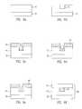
- FIGS. 4 a and 4 bare cross section views illustrating a process of fabricating a surface ridge planar optical device, in which processes according to embodiments of the present invention, are used.
- FIGS. 5 a - 5 eare cross section views illustrating a process of fabricating a buried ridge planar optical device, in which processes according to embodiments of the present invention, are used.
- FIGS. 6 a - 6 fare cross section views illustrating the process of fabricating a buried trench planar optical device, in which processes according to embodiments of the present invention, are used.
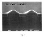
- FIG. 7is a scanning electron micrograph (SEM) of a layer deposited over a substrate patterned with trenches by a RF sputtering process including substrate bias, according to an embodiment of the present invention.
- a physical vapor deposition processprovides optical materials with controlled and uniform refractive index that meet the requirements for active and passive planar optical devices.
- the processuses radio frequency (RF) sputtering with a wide area target and a condition of uniform target erosion and includes multiple approaches for controlling refractive index.
- RFradio frequency
- FIG. 1 aAn apparatus 10 for RF sputtering of controlled refractive index material for planar optical devices is illustrated schematically in FIG. 1 a .
- the apparatusincludes a wide area sputter source target 12 which provides material to be deposited on substrate 16 .
- Substrate 16is positioned parallel to and opposite target 12 .
- Target 12functions as a cathode when RF power is applied to it and is equivalently termed the cathode.
- Target 12is a uniform source of material having a uniform index of refraction.
- Target 12is typically composed of pure materials such as quartz, alumina, or sapphire, (the crystalline form of alumina), or mixtures of compounds of optically useful materials.
- target 12is chemically uniform, flat, and of uniform thickness over an extended area.
- target 12is a composite target fabricated from individual tiles, precisely bonded together on a backing plate with minimal separation.
- a method of making chemically uniform tiles of mixed materials and attaching them to a backing plate 25 , forming target 12comprises another aspect of the present invention that is described in detail below.
- the complete target assemblyalso includes structures for cooling the target as described in U. S. Pat. No. 5,565,071 to Demaray et al, and incorporated herein by reference.
- substrate 16is a solid, smooth surface.
- substrate 16is a silicon wafer or a silicon wafer coated with a layer of silicon oxide formed by a chemical vapor deposition process or by a thermal oxidation process.
- substrate 16is a glass, such as Corning 1737 (Corning Inc., Elmira, N.Y.), a glass-like material, quartz, a metal, a metal oxide, or a plastic material.
- Substrate 16typically is supported on a holder or carrier sheet 17 that may be larger than substrate 16 .
- An essential feature of the present methodis that the area of wide area target 12 is greater than the area on the carrier sheet on which physically and chemically uniform deposition is accomplished. Secondly, it is also essential that a central region on target 12 , overlying the substrate 16 , be provided with a very uniform condition of sputter erosion of the target material. Uniform target erosion is a consequence of a uniform plasma condition. In the following discussion, all mention of uniform condition of target erosion is taken to be equivalent to uniform plasma condition. Uniform target erosion is evidenced by the persistence of film uniformity throughout an extended target life. A uniform deposited film is defined as a film having a nonuniformity in thickness, when measured at representative points on the entire surface of a substrate wafer, of less than about 5%.
- Thickness nonuniformityis defined, by convention, as the difference between the minimum and maximum thickness divided by twice the average thickness. If films deposited from a target from which more than about 20% of the weight of the target has been removed continue to exhibit thickness uniformity, then the sputtering process is judged to be in a condition of uniform target erosion for all films deposited during the target life.
- a uniform plasma conditionbe created in the region between the target and the substrate overlying the substrate.
- the region of uniform plasma conditionis indicated in the exploded view of FIG. 1 b .
- a plasmais created in the region denoted 51 , which extends under the entire target 12 .
- the central region of the target 52experiences the condition of uniform sputter erosion.
- a layer deposited on a substrate placed anywhere below central region 52will have uniform film thickness.
- the region in which deposition provides uniform film thicknessis larger than the area in which deposition provides a film with uniform physical or optical properties such as chemical composition or index of refraction.
- the targetit is essential that the target be planar or approximately planar for the formation of a film on a planar substrate which is to be coated with the material of the target.
- planarity of the targetmeans that all portions of the target surface in region 52 are within a few millimeters of a planar surface, typically within 0.5 mm.
- a first approachis to sputter without magnetic enhancement. Such operation is referred to as diode sputtering.
- a dielectric materialcan be deposited so as to provide suitably uniform film thickness over a central portion of an adjacent substrate area. Within that area, an area of highly uniform film may be formed with suitable optical uniformity.
- the rate of formation of films of many microns of thickness by diode sputteringcan be slow for small targets.
- a disadvantage in speed of diode sputteringcan be compensated by batch processing in which multiple substrates are processed at once.
- apparatus 10also includes a scanning magnet magnetron source 20 positioned above target 12 .
- a scanning magnetron source used for dc sputtering of metallic filmsis described in U.S. Pat. No. 5,855,744 to Halsey, et. al., (hereafter '744), which is incorporated herein by reference, and in references therein.
- the '744 patentdemonstrates the improvement in thickness uniformity that is achieved by reducing local target erosion due to magnetic effects in the sputtering of a wide area rectangular target. By reducing the magnetic field intensity at these positions, the local target erosion was decreased and the resulting film thickness nonuniformity was improved from 8%, to 4%, over a rectangular substrate of 400 ⁇ 500 mm.
- FIG. 2A top down view of magnet 20 and wide area target 12 is shown in FIG. 2.
- a film deposited on a substrate positioned on carrier sheet 17 directly opposed to the region of the target indicated by reference numeral 22has good thickness uniformity.
- Area 22is the same size as region 52 of the target, FIG. 1 b , that is exposed to a uniform plasma condition.
- carrier 17is coextensive with region 22 .
- Reference 24indicates the area below which both physically and chemically uniform deposition is achieved, where physical and chemical uniformity provide refractive index uniformity.
- FIG. 2indicates that the region 22 of the target providing thickness uniformity is, in general, larger than the region 24 of the target providing thickness and chemical uniformity. In optimized processes, however, regions 22 and 24 may be coextensive.
- Magnet 20extends beyond area 22 in one direction, the Y direction in FIG. 2, so that scanning is necessary in only one direction, the X direction, to provide a time averaged uniform magnetic field. As shown in FIGS. 1 a and 1 b , magnet 20 is scanned over the entire extent of target 12 which is larger than the region 52 of uniform sputter erosion. Magnet 20 is moved in a plane parallel to the plane of the target.
- a film with thickness nonuniformity of ⁇ 5%has been obtained on a substrate placed opposite a region of the target of dimension 300 ⁇ 400 mm.
- the thickness nonuniformity of a 300 mm diameter circular substrate at the center of this regioncan be less than ⁇ 3%.
- Refractive index nonuniformity at the 150 mm center of the region of less than one part in a thousandhas been obtained. The results reported here have been obtained, however, without extensive optimization.
- a useful general criterion for the present method of RF sputter depositionis that the wide area target be at least 1.5 times the area of the region on the carrier sheet on which physically uniform deposition is obtained. Since the carrier sheet can accommodate a single large substrate or multiple smaller substrates, the criterion can be expressed as the requirement that the area of the target be at least 1.5 times the area of the substrate.
- the present method using a wide area target with uniform sputter erosionoffers significant advantages over previous deposition approaches. It is possible to form a film with uniform thickness using a target that is smaller in plane area than the substrate. One way to do so is to move the substrate with respect to the source or cathode in such a fashion that the film formed is uniform in thickness. However, such a film will not have been formed under uniform process conditions, such as plasma density, the rate and angle of arrival of the vapor at the substrate, etc. Thus such films will not be uniform in physical properties such as density, refractive index, or resistivity, resulting in nonuniform optical and electrical performance.
- the conditions of sputtering at the target surfacesuch as the uniformity of erosion, the average temperature of the plasma at the target surface and the equilibration of the target surface with the gas phase ambient of the process are uniform over a region which is greater than or equal to the region to be coated with a uniform film thickness.
- the region of uniform film thicknessis greater than or equal to the region of the film which is to have highly uniform optical properties such as index of refraction, density, transmission or absorptivity.
- apparatus 10includes RF generator 14 for applying RF power to target 12 to generate a plasma in a background gas.
- RF generator 14is a high frequency source, conventionally operated at 13.56 MHz.
- Typical process conditions for RF sputter depositioninclude applying high frequency RF power in the range of about 500 to 5000 watts.
- An inert gas, typically argon,is used as the background sputtering gas.
- the deposition chamberis operated at low pressure, between about 0.5 millitorr and 8-10 millitorr. Typical process pressure is below about 2 millitorr where there are very few collisions in the gas phase, resulting in a condition of uniform “free molecular” flow. This ensures that the gas phase concentration of a gaseous component is uniform throughout the process chamber.
- background gas flow ratesin the range of about 30 to about 100 sccm, used with a pump operated at a fixed pumping speed of about 50 liters/second, result in free molecular flow conditions.
- the distance d, in FIG. 1 abetween the target and the substrate is varied between about 4 cm and 9 cm.
- a typical source to substrate distance dis 6 cm.
- the source to substrate distanceis chosen to optimize the thickness uniformity of the film. At large source to substrate distances the film thickness distribution is dome shaped with the thickest region of the film at the center of the substrate. At close source to substrate distance the film thickness is dish shaped with the thickest film formed at the edge of the substrate.
- the substrate temperatureis held constant in the range of about ⁇ 40° C. to about 550° C. and can be maintained at a chosen temperature to within about 10° C. by means of preheating the substrate and the substrate holder prior to deposition.
- the heat energy impressed upon the substrate by the processmust be conducted away from the substrate by cooling the table on which the substrate is positioned during the process, as known to those skilled in the art.
- the processis performed under conditions of uniform gas introduction, uniform pumping speed, and uniform application of RF power to the periphery of the target as known to skilled practitioners.
- the speed at which a scanning magnet 20 is swept over the entire targetis determined such that a layer thickness less than about 5 to 10 ⁇ , corresponding roughly to two to four monolayers of material, is deposited on each scan.
- the rate at which material is depositeddepends on the applied RF power and on the distance d, in FIG. 1 a , between the target 12 and the substrate 16 .
- scanning speeds between about 2 sec/one-way scan across the target to 20-30 sec/scanprovide a beneficial layer thickness. Limiting the amount of material deposited in each pass promotes chemical and physical uniformity.
- the rate of deposition of pure silicais approximately 0.8 ⁇ /kW-sec.
- the rate of depositionis 0.8 ⁇ /sec.
- a magnet scan speed that provides a scan of 2 secondsa film of 1.8 ⁇ nominal thickness is deposited.
- a thickness of 2.4 ⁇can be associated with one monolayer of amorphous silica film.
- the impingement rate of process gas equivalent to a monolayer per secondoccurs at approximately 1 ⁇ 10 ⁇ 6 torr.
- the process gasmay contain oxygen atoms ejected from the silica during sputtering in addition to the background inert gas.
- 4 ⁇ 10 3 monolayers of process gasimpinge on the film during the 4 second period of deposition.
- apparatus 10includes RF generator 15 , in addition to RF generator 14 described previously.
- RF generator 14is a high frequency source, typically 13.56 MHz, while RF generator 15 provides power at a much lower frequency, typically from about 100 to 400 kHz.
- Typical process conditions for dual frequency RF depositioninclude high frequency RF power in the range of about 500 to 5000 watts and low frequency RF power in the range of about 500 to 2500 watts where, for any given deposition, the low frequency power is from about a tenth to about three quarters of the high frequency power.
- the high frequency RF poweris chiefly responsible for sputtering the material of target 12 .
- the high frequencyaccelerates electrons in the plasma but is not as efficient at accelerating the much slower heavy ions in the plasma.
- Adding the low frequency RF powercauses ions in the plasma to bombard the film being deposited on the substrate, resulting in sputtering and densification of the film.
- the dual frequency RF deposition processgenerally results in films with a reduced surface roughness as compared with single frequency deposition.
- films with average surface roughness in the range of between about 1.5 and 2.6 nmhave been obtained with the dual frequency RF process.
- Experimental results for single and dual frequency depositionare further described in Example 4 below.
- reducing surface roughness of core and cladding materialsis key to reducing scattering loss in planar optical devices.
- the dual frequency RF processcan be used to tune the refractive index of the deposited film. Keeping the total RF power the same, the refractive index of the deposited film tends to increase with the ratio of low frequency to high frequency RF power.
- a core layer of a planar waveguidecan be deposited by a dual frequency RF process, and the same target 12 can be used to deposit a cladding layer using a single frequency RF process. Introducing low frequency RF power in the core layer deposition process can therefore be used to provide the difference in refractive index between core and cladding layer materials.
- RF power applied to the substratecan be either at the 13.56 MHz high frequency or at a frequency in the range of the low frequency RF.
- Substrate bias power similar to the high frequency RF powercan be used.
- Substrate biashas been used previously to planarize sputter deposited quartz films.
- a theoretical model of the mechanism by which substrate bias operateshas been put forward by Ting et al. (J. Vac. Sci. Technol. 15, 1105 (1978)).
- a so-called plasma sheathis formed about the substrate and ions are coupled from the plasma.
- the sheathserves to accelerate ions from the plasma so that they bombard the film as it is deposited, sputtering the film, and forward scattering surface atoms, densifying the film and eliminating columnar structure.
- the effects of adding substrate biasare akin to, but more dramatic than, the effects of adding the low frequency RF component to the sputter source.
- the filmis simultaneously deposited and etched.
- the net accumulation of film at any point on a surfacedepends on the relative rates of deposition and etching, which depend respectively, on the power applied to the target and to the substrate, and to the angle that the surface makes with the horizontal.
- the rate of etchingis greatest for intermediate angles, on the order of 45 degrees, that is between about 30 and 60 degrees.
- the target and substrate powerscan be adjusted such that the rates of deposition and etching are approximately the same for a range of intermediate angles.
- films deposited with bias sputteringhave the following characteristics. At a step where a horizontal surface meets a vertical surface, the deposited film makes an intermediate angle with the horizontal. On a surface at an intermediate angle, there will be no net deposition since the deposition rate and etch rate are approximately equal. There is net deposition on a vertical surface.
- a bias sputtering process without magnetic enhancementhas been observed to provide deposited films with exceptionally low surface roughness and exceptional refractive index uniformity.
- a silica film with an average surface roughness of 0.14 nm and a refractive index uniformity of less than 4 ⁇ 10 ⁇ 5 %has been obtained.
- diode bias sputteringproduces structures with the characteristic intermediate angle of the external surface of the film portion covering a raised ridge. Diode bias sputtering therefore, offers particular advantages for forming the core layer of certain waveguide structures, as further discussed in the '081 application.
- Dual frequency RF sputter deposition processes or single or dual frequency RF sputtering including substrate biasprovide dense films with excellent physical structure for use in planar optical devices.
- the present processesovercome problems that have been observed in the past in some conventionally deposited, particularly CVD deposited films, which can display so-called “columnar”, through thickness structure. In cross section, under magnification, the structure appears like a close packed group of columns or grains. Between the columns, there is often a diffusion path, referred to as “leader” defects.
- the columnar morphologycontributes to the roughness of the surfaces and sidewalls of conventional films after etching during fabrication into devices.
- the through thickness defects as well as the surface roughnessscatters guided light, resulting in insertion and transmission losses.
- the transparency of materials produced by dual frequency and substrate bias depositionis advantageous for building low loss optical devices.
- substrate biascan also influence the refractive index of the deposited film.
- an argon gas processit can be expected that substrate bias will result in densification and etching of the film.
- An argon bias processcan be expected to rise the index of a film deposited from a pure SiO 2 target.
- the rate of etchingis proportional to the local plasma density and that density is proportional to the local plasma density at the target cathode.
- the uniformity of the target plasmaas demonstrated by the uniformity of the nearby target erosion is very important for the uniformity of the effect of the substrate bias.
- use of substrate biasreinforces the benefits of the wide area target used under condition of uniform target erosion, of the present invention, to provide films with highly uniform optical properties.
- the refractive index of the material deposited using an RF sputtering processcan be deliberately tuned by modifying other plasma processing conditions, provided that such process conditions influence a substantially uniform region of a wide area cathode in a uniform way.
- raising the deposition temperatureincreases the refractive index of the resulting material.
- increasing the RF power applied to the targetincreases the refractive index of the deposited material.
- a reactive process gascan be added to the sputtering chamber which effectively modifies the chemical composition of the deposited material with a corresponding change in refractive index.
- adding a reducing gas, such as hydrogenincreases the refractive index and adding an oxidizer, such as oxygen, decreases the refractive index.
- Nitrogenis also a useful process gas. The direction of the effect on refractive index of replacing some of the argon with nitrogen depends on the chemical composition of the target.
- Example 1For example, as reported in detail in Example 1, for a pure silica, that is SiO 2 , target, increasing the process temperature from 40° C. to 400° C. results in an over 0.7% increase in refractive index, from 1.438 to 1.449.
- the process temperatureis the temperature at which the substrate carrier 17 is uniformly maintained. All refractive indices reported here are measured at 1550 nm. Increasing the process power from 800 W to 1200 W increases the refractive index of the deposited material by about 0.5%. Larger changes can be effected by using higher process power or by using reactive process gases in the sputtering chamber.
- Replacing a third of the argon with nitrogen at 150° C.provides an increase in refractive index of about 7%.
- Replacing argon as the sputtering gas with a mixture of 2% H 2 in Arresults in an increase in refractive index of over 2% at 150° C.
- target 12can be composed of silicon monoxide, SiO, which in the bulk state has a refractive index on the order of 1.8.
- RF sputtered SiO using argon as the sputtering gashas a refractive index slightly above 2, while SiO that was sputtered using a mixture of argon and nitrogen can have a refractive index lowered by over 15% to below 1.75, depending on the process conditions.
- the inventorsexplain the observed process gas effects on refractive index in the silicon/oxygen system in terms of free electron density on the silicon atoms in the material.
- Metallic silicon with a high electron densityhas a high refractive index, about 3.4.
- some of the oxygenis removed by collision with argon ions in the plasma, resulting in sputtered material with a higher refractive index than the SiO target.
- Nitrogen atomsare electronegative, but not as strongly electronegative as oxygen.
- the specific examples discussed to this pointhave focused on deposition from targets composed of oxides of silicon.
- the wide area target RF sputtering processis likewise advantageous for deposition of rare earth doped materials used for the core region of planar optical amplifiers.
- a target that is a mixture or compound of the rare earthtypically an oxide, fluoride, sulfide, or nitride, and a suitable oxide host is used.
- Er doped SiOpowdered SiO and Er 2 O 3 is thoroughly mixed, and formed into tiles by low temperature isostatic pressure.
- the present methodcan be applied to provide rare earth compounds doped in any of the combinations of oxides, including silica and alumina, or silica and alumina augmented by such other host material as yittria, zirconia, titania, or other materials that have been proposed for optical amplifier applications.
- a mixture of rare earth dopantscan be provided, as desired.
- Doping oxides of silicon with erbiumraises the refractive index of the doped material with respect to the refractive index of the host material.
- a film with an Er concentration of approximately 2 ⁇ 10 20 atoms/cm 3 in SiO, deposited by RF sputteringhas a refractive index that is 2.3% above that of RF sputtered SiO.
- the difference in refractive index between the doped core region and the cladding regionhas an important effect on the performance of planar optical amplifiers. For amplifiers, An values between about 0.25% and 15% are typically required.
- the index control methods described hereare beneficially used to provide cladding region materials with a suitable An with respect to the doped core region.
- tertiary, speciessuch as alkali, phosphorous, boron, and ceria have been introduced into optical layers for refractive index control, raising the index of the core or bringing the refractive index of the cladding up to a desired An from the refractive index of the doped core.
- tertiary speciescan diffuse into the core region and detrimentally interfere with rare earth ion luminescence.
- tertiary speciescan raise the coefficient of thermal expansion of the material causing stress and birefringence problems.
- the present method of wide area target RF sputtering with index controlavoids the disadvantages of index modification by tertiary additives.
- the wide area alloy targetbe completely uniform in chemical composition, at least to the level of the powder metallurgy utilized to form the powder mixture. Typical powder sizes are between tens and hundreds of microns. In the case of refractory oxide additions, it may be useful to pre-alloy these with the rare earth additions.
- Plasma spray, transient melting or induction meltingmay be utilized to form a powder which is a solution or alloy of such materials.
- the low sputter yield of pure aluminacan lead to segregation of the target material during sputtering. This causes the film to be low in aluminum with respect to the alloy target composition.
- the high solubility of the rare earth material in alumina and the high sputter efficiency of the rare earth doped aluminasuggest that practical formation of a sputter target material proceed through a first step of alloying the rare earth dopant and one or more of the host oxide additions to form a first powder material. The remainder of the host materials can be added prior to consolidation of the alloy target material. With this understanding the practitioner can fabricate alloy tiles of uniform composition.
- a method of forming targets 12 composed of individual tilesis provided.
- the consolidated materialIn order to form a wide area target of an alloy target material, the consolidated material must first be uniform to the grain size of the powder from which it is formed. It also must be formed into a structural material capable of forming and finishing to a tile shape having a surface roughness on the order of the powder size from which it is consolidated.
- the manufacture of indium tin oxide targets for wide area depositionhas shown that it is impractical to attempt to form a single piece, wide area target of fragile or brittle oxide material.
- the wide area sputter cathodeis therefore formed from a close packed array of smaller tiles.
- a target of a size used in the Examples hereinmay have from 2 to 20 individual tiles.
- the tilesare finished to a size so as to provide a margin of non-contact, tile to tile, 29 in FIG. 3, less than. 0.010′′ to 0.020′′ or less than half a millimeter so as to eliminate plasma process between the tiles.
- the distance of the target tile assembly comprising target 12 to the dark space anode or ground shield 19 , in FIGS. 1 a and 1 bcan be somewhat larger so as to provide non contact assembly or provide for thermal expansion tolerance during process chamber conditioning or operation.
- the low thermal expansion and fragile condition of ideal optical dielectric tile materialcan be a cause of great difficulty in bonding and processing a wide area array of such tiles.
- the bonding process according to the present inventionthat overcomes these difficulties is illustrated in FIG. 3 .
- Sputter coating a side of such a tile in region 26 prior to bonding with backing plate 25can be accomplished with a layer of a material such as chrome or nickel as a diffusion layer.
- Such a metallurgical layeracts as a wetting layer to be tinned with a suitable solder material such as indium or an indium alloy.
- the backing plate 25should be made of titanium or molybdenum or other low expansion metal so as to provide a good match with the thermal expansion of the tile material.
- a very important aspect of the formation of a tiled targetis the finishing and coating of the backing plate prior to the solder bonding of the array of tiles.
- the portion 27 of the backing plate to be exposed to vacuum, either between the tiles or about the periphery or dark space region of the tile assemblyshould be bead blasted and plasma spray coated with a material such as alumina or silica to prevent contamination of the process by the target backing plate material.
- the portion 26 of the backing plate beneath the tileshould be sputter coated with a material such as nickel or chrome to enable solder bonding. Pure indium solder, although it has a higher melting point than alloys such as indium-tin, is much more ductile.
- solderThis allows the solder to yield during cooling of the solder bonded assembly relieving stress on the bonded tiles. It is useful to provide an outer frame fixture which is located precisely for the location of the outer tiles. It is also useful to provide shim location, tile to tile, while the assembly is at temperature. The actual solder application and lay up procedure can be devised by those versed in solder assembly. It is essential for reasons of heat transfer that the solder forms a full fill of the volume between the tile and the backing plate. It is also essential that the solder not be exposed to the plasma. There should not be any visible solder in the region between the tiles or on the backing plate. To enable this condition it is useful to sputter coat the wetting layer area with an offset 28 of several millimeters on both the tile and the backing plate.
- solder materialwill not wet region 28 upon assembly.
- a mask for the sputter deposition of the diffusion barrier/wetting layer filmis useful.
- cleaning of the bonded target tile assemblyshould utilize anhydrous cleaning rather than aqueous based cleaning methods.
- RF sputtering methods for material depositionare combined with processes commonly used in semiconductor fabrication, such as photo-lithographic patterning and etching, to produce planar optical devices.
- a process to produce a surface ridge deviceis illustrated schematically in the device cross sections of FIGS. 4 a and 4 b .
- RF sputteringis used to deposit a layer of cladding material 34 on a substrate 32 .
- a layer of core material 36having a higher index of refraction than the cladding layer is then deposited by RF sputtering on the cladding layer 34 , followed by another layer 34 of the cladding material, as shown in FIG. 4 a .
- a ridge structure 31is then formed in the upper cladding layer and a portion of the core material, as required by the design of the waveguide, by means of lithography and etching, FIG. 4 b .
- the ridge 31serves to guide the light in the core material.
- the core materialis doped with a photoluminescent active material and the conditions for amplification are met, such a structure may be used as a planar waveguide amplifier device.
- FIGS. 5 a - 5 eillustrate the steps of forming a buried ridge planar wave-guide.
- FIG. 5 ashows the same sequence of films as FIG. 4 a without the upper cladding layer.
- FIG. 5 bshows a ridge 37 that has been formed by lithography and etching from the core layer 36 . The ridge is shown as unity aspect ratio but might have another aspect in cross section.
- FIG. 5 cillustrates the conformity or ridge coverage shape 38 of an overlayer of the cladding material formed by means of standard RF sputtering. The line of sight arrival of the sputtered cladding material results in poor step coverage of those portions of the ridge having low solid angle exposure to the sputter cathode source.
- the filmgrows in a lateral direction from the upper comers of the ridge resulting in a ‘bread loaf’ shape.
- the overhang of the lateral growthcauses the rate of deposition to decrease at the lower comer of the ridge.
- a ‘bird's beak’ shaped defect in the coverageis formed in the covering film.
- defectis the cause of electrical breakdown of an insulating dielectric layer.
- a buried ridge wave-guide having an upper cladding as shown in FIG. 5 cwould demonstrate poor single mode confinement and substantial polarization dependence for the guided light due to the ‘bird's beak’ defect. Substantial insertion loss would result from the roughness introduced by the defect in the longitudinal direction of the wave-guide.
- FIG. 5 dillustrates the effect of dual frequency RF deposition on the formation of the coverage of the ridge.
- a small amount of ion bombardment of the cladding layer 39can be achieved during deposition, providing a small etch rate to reduce the lateral growth of the deposition on the top comers of the ridge.
- the small etch rate during depositionreduces the shadowing at the lower comer of the ridge and increases the step coverage.
- the low amount of ion bombardmentalso acts to densify the film by forward scattering of the adsorbed, sputtered material and provides for increased mobility of the sputtered material on the surface of the film. Both effects act to reduce the leader defect shown in FIG. 5 c .
- 5 dshows the improved step coverage 39 that can result from the application of dual frequency power for the sputter deposition of the upper cladding. Due to the fact that the lower frequency, of the dual frequency process, is applied to the cathode, the deposition rate will increase with the addition of the second frequency power. Thus, the positive effect of the second frequency can not be isolated from the deposition rate.
- the structure, shown in FIG. 5 dis not an ideal structure for the formation of a light wave guiding device because the step coverage defect has not been eliminated.
- FIG. 5 eshows the effect of the addition of substrate bias during the sputter deposition of the upper cladding layer.
- the substrate bias poweris independent of the source power.
- the addition of further bias power to the substratewill increase the etch rate. In practice it may be equal to the source power.
- the rate of deposition of the filmwill be significantly greater on the horizontal features of the substrate then the rate of etching. However, due to the efficiency of ion etching of a feature of the film inclined near 45 degrees from the horizontal surface, the net accumulation at that angle may be very low.
- an angle of constant reposecan be impressed upon the accumulation shape of the deposited cladding layer.
- FIG. 5 eshows schematically the step coverage that can be obtained in the cladding layer 40 by bias sputtering.
- FIG. 7demonstrates that the smooth, straight sidewalls and characteristic 45 degree angles depicted schematically in FIG. 5 e are achieved in practice. In particular, the leader defect and the shadowing effect of unbiased deposition can be completely eliminated.
- the step coveragecan be increased by increasing the thickness of layer 40 . While the discussion above has emphasized the beneficial geometrical effects of bias sputtering deposition of cladding layer 40 , it is also useful to use bias sputtering to deposit all the layers of planar optical devices because of the increased transparency of bias sputtered materials. Also, since bias sputtering affects refractive index, it is desirable to use bias sputtering for both lower and upper cladding layers in order for the cladding layers to have the same refractive index.
- a wave guide device 30as shown in FIG. 5 e , with very low polarization dependence and high quality mode containment can be obtained in a material such as pure silica. If such a device is realized in pure silica without the use of dopants, substantial improvement in thermal stability over present devices can be achieved.
- Device 30may be used as a wave-guide or splitter. When the core is rare earth doped, it may be utilized to form an active device such as an optical amplifier. When formed by thin film methods, arrays of such devices may be created. Exemplary dimensions of the cross section of ridge 31 or 37 or core 46 , discussed below, are from about 2 ⁇ 2 ⁇ m to about 9 ⁇ 9 ⁇ m. Exemplary dimensions for cladding layer 34 is between about 10 and 25 ⁇ m thick.
- FIGS. 6 a - 6 fThe process of forming a trench device 50 is shown schematically in FIGS. 6 a - 6 f .
- a thick layer 41 of cladding materialis deposited by RF sputtering on substrate 32 , FIG. 6 a .
- a trench 42is formed by photo-lithographic patterning and etching in cladding layer 41 , FIG. 6 b .
- Core material 43may be RF sputtered into the trench, FIG. 6 c .
- the maximum thickness of the bottom fill of an aspect one trench with a film of unity thicknessmay be less than 10 to 20%.
- the core layercan close off, leaving a void in the trench.
- the best prior artteaches that the film 43 should be etched back.
- An etch back processremoves the surface layer, opens the void if one has formed and leaves the partial fill in the trench, (see H. Ohkubo, et. al. “Polarization-Insensitive Arrayed-Waveguide Grating Using Pure SiO 2 Cladding, Proc. OECC 2000, Technical Digest, July 2000, Makuhari Messe, Japan.).
- a second depositioncan fill the partially filled trench.
- FIG. 6 dshows the cladding layer applied by means of a dual frequency process. Using dual frequency, layer 44 remains open due to the etching influence of the second lower frequency. The bottom fill can increase to as much as 60 to 80%. While dual RF deposition is more successful at filling the trench than single frequency deposition, the process is not ideal for fabrication of buried trench waveguides.
- a trenchcan be filled in a single process step using bias sputtering.
- FIG. 6 eschematically shows core material deposited by means of RF bias sputtering of layer 45 .
- FIG. 7demonstrates complete trench fill has been achieved in practice with bias sputtering.
- the structure of FIG. 6 ecan be etched back by means of a bias process with the net rate of bias etching greater than the rate of deposition on the horizontal surface. It can also be mechanically polished or etched back.
- Deposition of a cladding layer by means of RF sputteringresults in device 50 shown in FIG. 6 f .
- Device 50can be used as a polarization independent wave guide.
- the core materialwas doped with germania to raise the index of refraction.
- the control of the index of deposited pure silicacan be used to provide the higher index material of the core as a uniform layer.
- the wide area magnetron RF sourcewill also provide a uniform plasma condition for the application of the uniform bias sputtering.
- Ohkubo, et. al.utilize a three step process of deposition, etch back and deposition to fill a trench between two ridge waveguide structures.
- two core waveguide structuresformed either by etching a ridge or filling a trench, are brought together either to merge, thus forming a so called ‘3 dB’ junction, or into close proximity so as to form a coupler.
- 3 dBso called ‘3 dB’ junction
- couplernarrow, deep structures are formed.
- the trench fill, the ridge coverage and the adjacent structure fillcan be accomplished uniformly in the subject wide area RF bias sputtering process.
- ⁇ nmay be chosen from 0.1 to 0.8 percent for the purpose of weak mode confinement at a wavelength or for control of the numerical aperture of a waveguide device.
- the index differencemay need to be uniform to ⁇ 5% of the difference for each film.
- the overall nonuniformity of each film, 1 percent of 5 percentis 5 ⁇ 10 ⁇ 4 . Evaluated at a nominal index of 1.50, such a nonuniformity corresponds to a variance of 0.00075 for each film.
- the nonuniformity of index reported here and achieved by means of wide area RF sputteringis, on first result, very close to the estimated value required for each film.
- An AKT 1600 series PVD production reactor(Applied Komatsu Technology, Santa Clara, Calif.) modified for RF application with custom ceramic tile targets was used for RF sputter deposition of SiO 2 .
- a wide area target of dimension 550 ⁇ 650 mmwas fabricated from four quartz tiles, each 4 mm thick, Corning code 9780 glass (Coming Inc. Elmira, N.Y.).
- the tileswere finished to a smooth surface, chemically cleaned, rinsed with hot deionized water, dried, and sputter coated with several microns of chrome.
- the chrome coated sideswere bonded to a thin plate of titanium as described above.
- the titanium backing platewas prepared for bonding by bead blasting, chemical cleaning, and plasma coating with silicon.
- the tiles and the backing platewere heated to approximately 180° C. and regions were coated with a layer of liquid indium.
- the tileswere precisely placed on the backing plate such that they were separated by no more than 0.02 inches from each other and from the edges of the region exposed to the plasma.
- a 150 mm p-type silicon wafer substratewas placed in the center of a 400 ⁇ 500 mm glass carrier sheet. 800 watts of power was applied to the target at 13.56 MHz. A race-track shaped magnet of approximate dimension 150 mm ⁇ 600 mm was swept over the face of the target at a rate of 4 seconds per one-way scan (8 seconds per complete cycle.) Substrate temperature was uniformly held at 40° C. and the sputter gas was 99.99999% pure argon at a flow rate of 60 sccm. The target to substrate distance was 6.5 cm. Deposition efficiency was approximately 0.8 ⁇ kW-sec. Film thickness and index of refraction were measured at five equally spaced points over the full face of the wafer using a FilmTek 4000 interferometer. Refractive index at 1550 nm was 1.437998 ⁇ 0.001297 (0.09%); film thickness was 9227.66 nm with a nonuniformity of 6.8%. Results are included as Sample A in Table 1 below.
- SiO 2 filmswere deposited by processes analogous to that described in Example 1, varying deposition temperature, applied power, and process gas. Results are tabulated in Table 1 below.
- Target tiles of SiOwere prepared from a powder of SiO by low temperature isostatic pressure. The tiles were cut and bonded to a backing plate as described above.
- Mixed oxide tiles used to deposit erbium doped SiOwere prepared by mixing powdered Er 2 O 3 and SiO in a ratio of 2 molar cation percent erbia.
- SiO and Er doped SiO filmswere deposited as in Examples 1 and 2 above. Refractive index and thickness are tabulated for SiO in Table 2 and for Er doped SiO (SiO:Er) with an Er concentration of approximately 2 ⁇ 10 20 Er atoms/ cm 3 , in Table 3.
- AKT 1600 series PVD production reactor and wide area target as described in Example 1was used.
- High frequency (13.56 MHz) and low frequency (about 350 kHz) process powersare listed along with surface roughness and refractive index (RI) of the deposited films in Table 4 below.
- Depositionswere all conducted at Ar flow rates of 40 standard cubic centimeters per minute (sccm) and at or near room temperature, except as noted below.
- Refractive index at 1.5 ⁇ mwas measured using a Film Tek 4000 normal incidence interferometer (SCI, Encinitas, Calif.).
- Average surface roughness, R awas determined from Atomic Force Microscopy (AFM) measurements using a NanoScope III 5000 instrument (Digital Instruments, Veeco Metrology Group, Santa Barbara, Calif.)
- Films deposited with a single frequency RF processhad average surface roughness values in the range of 2.8 to 3.4 nm while the dual frequency process produced films with systematically lower average surface roughness of between 1.4 and 2.6 nm. Keeping other process conditions the same, increasing the ratio of low frequency to high frequency power is seen to result in decreasing surface roughness. Refractive index is observed to have the opposite proportional dependence on power ratio; increasing the low frequency power contribution results in films with higher refractive index. Beneficially, the higher refractive index material has the lower average surface roughness.
- core layer materialcan be obtained by using dual frequency deposition without use of dopants to modify the index of either layer, while using only the high frequency component produces a material of lower refractive index suitable for the cladding layer.
- An AKT 4300 series PVD production reactor(Applied Komatsu Technology, Santa Clara, Calif.) modified to accept custom ceramic tile targets and modified to induce a voltage on the substrate was used to deposit silica on planar and patterned 100 mm silicon wafers.
- a wide area target of dimension 750 ⁇ 870 mmwas fabricated as described in Example 1.
- the waferswere placed in the center of a Corning code 1739 glass carrier sheet opposite the target.
- the reactorwas operated in the diode sputtering mode, without magnetic enhancement, at a high frequency RF power of 2500 W and an induced voltage of ⁇ 400V.
- a bias voltage of ⁇ 125 V at 2 MHz and 250 Wwas induced on the substrate.
- An argon gas flow rate of 160 sccmwas used.
- FIG. 7shows an SEM image of a silica film deposited over a patterned substrate.
- the trenches in the patterned substrateare seen to be completely and uniformly filled and the ridges are uniformly covered.
- the top surface of the layer overlying the ridgesis flat and the sloping sides of the layer overlying the ridges are nominally at 45 degree angles. All of the foregoing geometric features are characteristic of bias sputtering deposition. As reported above, for trench features with unit aspect ratio, the maximum thickness at the bottom of the trench of films deposited by conventional RF sputtering is less than about 10-20%.
Landscapes
- Chemical & Material Sciences (AREA)
- Physics & Mathematics (AREA)
- Engineering & Computer Science (AREA)
- Organic Chemistry (AREA)
- Mechanical Engineering (AREA)
- Metallurgy (AREA)
- Materials Engineering (AREA)
- Microelectronics & Electronic Packaging (AREA)
- Chemical Kinetics & Catalysis (AREA)
- General Physics & Mathematics (AREA)
- Optics & Photonics (AREA)
- Physical Vapour Deposition (AREA)
- Optical Integrated Circuits (AREA)
Abstract
Description
| TABLE 1 |
| SiO2Thickness and Refractive Index as Function of Deposition Conditions |
| Power | Temperature | Sputtering gas/ | Refractive index* at | ||
| (watts) | (° C.) | Flow rate (sccm) | 1550 nm | Thickness (nm)# | |
| A | 800 | 40 | Ar/60 | 1.437998 (0.001297) | 9227.66 (6.8%) |
| B | 800 | 150 | Ar/60 | 1.440923 (0.001979) | 3133.25 |
| C | 800 | 400 | Ar/60 | 1.450126 (0.000726) | 9295.86 (4.8%) |
| D | 1200 | 150 | Ar/60 | 1.448610 (0.000976) | 9.2 × 10³ |
| E | 800 | 150 | 2% H2in Ar/60 | 1.462198 (0.001809) | 1287.15 |
| F | 800 | 150 | N2/20, Ar/40 | 1.580249 (0.008346) | 608.87 |
| G | 1400 | 150 | N2/20, Ar/40 | 1.548439 (0.006499) | 2354.80 |
| H | 800 | 400 | Ar/60 | 1.450036 (0.000702) | 9295.84 (4.8%) |
| *Standard deviation (1σ) in parentheses | |||||
| #Thickness nonuniformity | |||||
| TABLE 2 |
| SiO Thickness and Refractive Index as Function of Deposition Conditions |
| Refractive | |||||
| Power | Temperature | Sputtering gas/ | index* at | Thickness | |
| (watts) | (° C.) | Flow rate (sccm) | 1550 nm | (nm) | |
| J | 1000 | 150 | Ar/60 | 2.084500 | 691.78 |
| K | 1000 | 150 | N2/10, Ar/50 | 1.736693 | 1000.96 |
| (0.010250) | |||||
| L | 1000 | 150 | N2/25, Ar/50 | 1.740680 | 770.08 |
| *Standard deviation (1σ) in parentheses | |||||
| TABLE 3 |
| SiO:Er Thickness and Refractive Index as Function of Deposition |
| Conditions |
| Refractive | |||||
| Power | Temperature | Sputtering gas/ | index* at | Thickness | |
| (watts) | (° C.) | Flow rate (sccm) | 1550 nm | (nm) | |
| M | 1000 | 150 | Ar/60 | 2.132870 | 791.35 |
| N | 1000 | 150 | N2/10, Ar/50 | 1.740480 | 1501.04 |
| (0.017838) | |||||
| O | 1000 | 150 | N2/25, Ar/50 | 1.750910 | 1400.11 |
| P | 1000 | 150 | N2/50, Ar/25 | 1.792790 | 786.78 |
| Q | 800 | 400 | O2/3, Ar/57 | 1.454825 | 1159.50 |
| (0.005425) | |||||
| *Standard deviation (1σ) in parentheses | |||||
| TABLE 4 |
| Average Surface Roughness and Refractive Index of RF Sputtered Silica |
| HF | LF | LF/HF | ||||
| Power | Power | Total | Power | |||
| EXAMPLE | (kW) | (kW) | Ra(nm) | RI | Power | Ratio |
| A | 2.3 | — | 2.988 | 1.4492 | 2.300 | 0 |
| B | 2.3 | — | 2.804 | 1.4494 | 2.300 | 0 |
| C | 2.3 | — | 3.412 | 1.4473 | 2.300 | 0 |
| D | 2.0 | 0.350 | 1.818 | 1.4538 | 2.350 | 0.175 |
| E | 2.0 | 0.350 | 1.939 | 1.4533 | 2.350 | 0.175 |
| F | 2.0 | 0.350 | 2.007 | 1.4547 | 2.350 | 0.175 |
| G | 2.0 | 0.350 | 2.571 | 1.4520 | 2.350 | 0.175 |
| H | 1.7 | 0.600 | 1.729 | 1.4560 | 2.300 | 0.353 |
| I | 1.7 | 1.000 | 1.445 | 1.4617 | 2.700 | 0.588 |
| J | 3.0 | 0.525 | 2.359 | 1.4542 | 3.525 | 0.175 |
| K* | 2.0 | 0.350 | 3.419 | 1.4523 | 2.350 | 0.175 |
| L# | 3.0 | 0.525 | 4.489 | 1.4449 | 3.525 | 0.175 |
| *Deposition temperature 225° C. | ||||||
| #Ar flow rate 120 sccm | ||||||
Claims (32)
Priority Applications (5)
| Application Number | Priority Date | Filing Date | Title |
|---|---|---|---|
| US09/903,050US6506289B2 (en) | 2000-08-07 | 2001-07-10 | Planar optical devices and methods for their manufacture |
| PCT/US2001/022750WO2002012932A2 (en) | 2000-08-07 | 2001-07-18 | Methods for manufacturing planar optical devices |
| AU2001277002AAU2001277002A1 (en) | 2000-08-07 | 2001-07-18 | Methods for manufacturing planar optical devices |
| TW090119173ATW520450B (en) | 2000-08-07 | 2001-08-06 | Planar optical devices and methods for their manufacture |
| US10/288,278US6827826B2 (en) | 2000-08-07 | 2002-11-04 | Planar optical devices and methods for their manufacture |
Applications Claiming Priority (2)
| Application Number | Priority Date | Filing Date | Title |
|---|---|---|---|
| US63330700A | 2000-08-07 | 2000-08-07 | |
| US09/903,050US6506289B2 (en) | 2000-08-07 | 2001-07-10 | Planar optical devices and methods for their manufacture |
Related Parent Applications (1)
| Application Number | Title | Priority Date | Filing Date |
|---|---|---|---|
| US63330700AContinuation-In-Part | 2000-08-07 | 2000-08-07 |
Related Child Applications (1)
| Application Number | Title | Priority Date | Filing Date |
|---|---|---|---|
| US10/288,278DivisionUS6827826B2 (en) | 2000-08-07 | 2002-11-04 | Planar optical devices and methods for their manufacture |
Publications (2)
| Publication Number | Publication Date |
|---|---|
| US20020033330A1 US20020033330A1 (en) | 2002-03-21 |
| US6506289B2true US6506289B2 (en) | 2003-01-14 |
Family
ID=27091844
Family Applications (2)
| Application Number | Title | Priority Date | Filing Date |
|---|---|---|---|
| US09/903,050Expired - LifetimeUS6506289B2 (en) | 2000-08-07 | 2001-07-10 | Planar optical devices and methods for their manufacture |
| US10/288,278Expired - LifetimeUS6827826B2 (en) | 2000-08-07 | 2002-11-04 | Planar optical devices and methods for their manufacture |
Family Applications After (1)
| Application Number | Title | Priority Date | Filing Date |
|---|---|---|---|
| US10/288,278Expired - LifetimeUS6827826B2 (en) | 2000-08-07 | 2002-11-04 | Planar optical devices and methods for their manufacture |
Country Status (4)
| Country | Link |
|---|---|
| US (2) | US6506289B2 (en) |
| AU (1) | AU2001277002A1 (en) |
| TW (1) | TW520450B (en) |
| WO (1) | WO2002012932A2 (en) |
Cited By (49)
| Publication number | Priority date | Publication date | Assignee | Title |
|---|---|---|---|---|
| US20020136518A1 (en)* | 2001-03-21 | 2002-09-26 | Wang Everett X. | Fabrication of optical waveguides for reduction of minimum waveguide spacing |
| US20030063883A1 (en)* | 2001-07-10 | 2003-04-03 | Demaray Richard E. | As-deposited planar optical waveguides with low scattering loss and methods for their manufacture |
| US20030134054A1 (en)* | 2001-11-09 | 2003-07-17 | Demaray Richard E. | Low temperature zirconia based thermal barrier layer by PVD |
| US20030175142A1 (en)* | 2002-03-16 | 2003-09-18 | Vassiliki Milonopoulou | Rare-earth pre-alloyed PVD targets for dielectric planar applications |
| US20030173207A1 (en)* | 2002-03-16 | 2003-09-18 | Symmorphix, Inc. | Biased pulse DC reactive sputtering of oxide films |
| US20040099817A1 (en)* | 2002-11-21 | 2004-05-27 | Demos Alexandros T. | Large area source for uniform electron beam generation |
| US20040105644A1 (en)* | 2002-08-27 | 2004-06-03 | David Dawes | Optically coupling into highly uniform waveguides |
| US20040259305A1 (en)* | 2003-05-23 | 2004-12-23 | Demaray Richard E. | Energy conversion and storage films and devices by physical vapor deposition of titanium and titanium oxides and sub-oxides |
| US20050000794A1 (en)* | 2003-05-23 | 2005-01-06 | Demaray Richard E. | Transparent conductive oxides |
| US20050013972A1 (en)* | 2003-07-18 | 2005-01-20 | Daisuke Kusabiraki | Large-size substrate |
| US20060112730A1 (en)* | 2004-11-26 | 2006-06-01 | Hon Hai Precision Industry Co., Ltd. | Core insert for a glass molding machine, and an apparatus for making the same |
| US20060134522A1 (en)* | 2004-12-08 | 2006-06-22 | Hongmei Zhang | Deposition of LiCoO2 |
| US20060286448A1 (en)* | 2002-08-09 | 2006-12-21 | Snyder Shawn W | Electrochemical apparatus with barrier layer protected substrate |
| US20070053139A1 (en)* | 2005-09-02 | 2007-03-08 | Hongmei Zhang | Deposition of perovskite and other compound ceramic films for dielectric applications |
| US7205662B2 (en) | 2003-02-27 | 2007-04-17 | Symmorphix, Inc. | Dielectric barrier layer films |
| US20070125638A1 (en)* | 2004-12-08 | 2007-06-07 | Infinite Power Solutions, Inc. | DEPOSITION OF LiCoO2 |
| US20070184345A1 (en)* | 2002-08-09 | 2007-08-09 | Infinite Power Solutions, Inc. | Hybrid Thin-Film Battery |
| US20070202395A1 (en)* | 2002-08-09 | 2007-08-30 | Infinite Power Solutions | Metal film encapsulation |
| US20070289869A1 (en)* | 2006-06-15 | 2007-12-20 | Zhifei Ye | Large Area Sputtering Target |
| US20080078496A1 (en)* | 2006-09-29 | 2008-04-03 | Snyder Shawn W | Masking of and material constraint for depositing battery layers on flexible substrates |
| US20080173542A1 (en)* | 2006-11-07 | 2008-07-24 | Neudecker Bernd J | SPUTTERING TARGET OF Li3PO4 AND METHOD FOR PRODUCING SAME |
| US20080200002A1 (en)* | 2004-10-19 | 2008-08-21 | Tokyo Electron Limited | Plasma Sputtering Film Deposition Method and Equipment |
| EP1970465A2 (en) | 2007-03-13 | 2008-09-17 | JDS Uniphase Corporation | Method and sputter-deposition system for depositing a layer composed of a mixture of materials and having a predetermined refractive index |
| US20080261107A1 (en)* | 2002-08-09 | 2008-10-23 | Snyder Shawn W | Robust metal film encapsulation |
| US20080286651A1 (en)* | 2002-08-09 | 2008-11-20 | Neudecker Bernd J | Hybrid Thin-Film Battery |
| US20090159433A1 (en)* | 2007-12-21 | 2009-06-25 | Neudecker Bernd J | Method for Sputter Targets for Electrolyte Films |
| US7565084B1 (en) | 2004-09-15 | 2009-07-21 | Wach Michael L | Robustly stabilizing laser systems |
| US20090251099A1 (en)* | 2008-04-02 | 2009-10-08 | Brantner Paul C | Passive over/under voltage control and protection for energy storage devices associated with energy harvesting |
| US20090288943A1 (en)* | 2008-05-21 | 2009-11-26 | Byung Sung Kwak | Thin film batteries and methods for manufacturing same |
| US20090307896A1 (en)* | 2002-08-09 | 2009-12-17 | Snyder Shawn W | Electrochemical Apparatus With Barrier Layer Protected Substrate |
| US20100068995A1 (en)* | 2008-09-12 | 2010-03-18 | Brantner Paul C | Energy Device With Integral Conductive Surface For Data Communication Via Electromagnetic Energy And Method Thereof |
| US20100090655A1 (en)* | 2008-10-08 | 2010-04-15 | Keating Joseph A | Environmentally-Powered Wireless Sensor Module |
| US20100294428A1 (en)* | 2009-05-20 | 2010-11-25 | Snyder Shawn W | Method of Integrating Electrochemical Devices Into and Onto Fixtures |
| US20110048781A1 (en)* | 2009-09-01 | 2011-03-03 | Neudecker Bernd J | Printed circuit board with integrated thin film battery |
| US7901870B1 (en) | 2004-05-12 | 2011-03-08 | Cirrex Systems Llc | Adjusting optical properties of optical thin films |
| US8045832B2 (en) | 2002-03-16 | 2011-10-25 | Springworks, Llc | Mode size converter for a planar waveguide |
| US8268488B2 (en) | 2007-12-21 | 2012-09-18 | Infinite Power Solutions, Inc. | Thin film electrolyte for thin film batteries |
| US8404376B2 (en) | 2002-08-09 | 2013-03-26 | Infinite Power Solutions, Inc. | Metal film encapsulation |
| US8518581B2 (en) | 2008-01-11 | 2013-08-27 | Inifinite Power Solutions, Inc. | Thin film encapsulation for thin film batteries and other devices |
| US8736947B2 (en) | 2009-10-23 | 2014-05-27 | Applied Materials, Inc. | Materials and device stack for market viable electrochromic devices |
| US8906523B2 (en) | 2008-08-11 | 2014-12-09 | Infinite Power Solutions, Inc. | Energy device with integral collector surface for electromagnetic energy harvesting and method thereof |
| US9136569B2 (en) | 2008-05-21 | 2015-09-15 | Applied Materials, Inc. | Microwave rapid thermal processing of electrochemical devices |
| US9356316B2 (en) | 2012-04-18 | 2016-05-31 | Applied Materials, Inc. | Pinhole-free solid state electrolytes with high ionic conductivity |
| US9366816B2 (en) | 2012-11-12 | 2016-06-14 | Demaray, Llc | Adiabatic planar waveguide coupler transformer |
| US9593405B2 (en) | 2011-06-17 | 2017-03-14 | Applied Materials, Inc. | Pinhole-free dielectric thin film fabrication |
| US9634296B2 (en) | 2002-08-09 | 2017-04-25 | Sapurast Research Llc | Thin film battery on an integrated circuit or circuit board and method thereof |
| US20200018900A1 (en)* | 2018-07-13 | 2020-01-16 | United States Of America, As Represented By The Secretary Of The Navy | Optical Waveguide |
| US10680277B2 (en) | 2010-06-07 | 2020-06-09 | Sapurast Research Llc | Rechargeable, high-density electrochemical device |
| US10818909B2 (en) | 2016-05-09 | 2020-10-27 | Demaray, Llc | Energy storage device with a first metal layer formed from a precursor layer upon charge and diffused into a cathode during discharge |
Families Citing this family (40)
| Publication number | Priority date | Publication date | Assignee | Title |
|---|---|---|---|---|
| US6705124B2 (en)* | 2001-06-04 | 2004-03-16 | Lightwave Microsystems Corporation | High-density plasma deposition process for fabricating a top clad for planar lightwave circuit devices |
| US20030033834A1 (en)* | 2001-08-17 | 2003-02-20 | Michael Bazylenko | Method of depositing a cladding layer |
| JP4139605B2 (en) | 2002-03-01 | 2008-08-27 | 大日本印刷株式会社 | Method for determining mask cross-sectional structure in single-sided-type substrate excavation type phase shift mask |
| DE10222909A1 (en)* | 2002-05-22 | 2003-12-04 | Unaxis Balzers Ag | Sputtering process or device for the production of coatings optimized for residual stress |
| US7297247B2 (en)* | 2003-05-06 | 2007-11-20 | Applied Materials, Inc. | Electroformed sputtering target |
| US7431857B2 (en)* | 2003-08-15 | 2008-10-07 | Applied Materials, Inc. | Plasma generation and control using a dual frequency RF source |
| US7510665B2 (en)* | 2003-08-15 | 2009-03-31 | Applied Materials, Inc. | Plasma generation and control using dual frequency RF signals |
| US20050106873A1 (en)* | 2003-08-15 | 2005-05-19 | Hoffman Daniel J. | Plasma chamber having multiple RF source frequencies |
| US7910218B2 (en) | 2003-10-22 | 2011-03-22 | Applied Materials, Inc. | Cleaning and refurbishing chamber components having metal coatings |
| US7838430B2 (en)* | 2003-10-28 | 2010-11-23 | Applied Materials, Inc. | Plasma control using dual cathode frequency mixing |
| US20060027329A1 (en)* | 2004-08-09 | 2006-02-09 | Sinha Ashok K | Multi-frequency plasma enhanced process chamber having a torroidal plasma source |
| US7601246B2 (en)* | 2004-09-29 | 2009-10-13 | Lam Research Corporation | Methods of sputtering a protective coating on a semiconductor substrate |
| US7670436B2 (en) | 2004-11-03 | 2010-03-02 | Applied Materials, Inc. | Support ring assembly |
| US20060278521A1 (en)* | 2005-06-14 | 2006-12-14 | Stowell Michael W | System and method for controlling ion density and energy using modulated power signals |
| US8617672B2 (en) | 2005-07-13 | 2013-12-31 | Applied Materials, Inc. | Localized surface annealing of components for substrate processing chambers |
| US7762114B2 (en)* | 2005-09-09 | 2010-07-27 | Applied Materials, Inc. | Flow-formed chamber component having a textured surface |
| US9127362B2 (en)* | 2005-10-31 | 2015-09-08 | Applied Materials, Inc. | Process kit and target for substrate processing chamber |
| US8647484B2 (en) | 2005-11-25 | 2014-02-11 | Applied Materials, Inc. | Target for sputtering chamber |
| US20070283884A1 (en)* | 2006-05-30 | 2007-12-13 | Applied Materials, Inc. | Ring assembly for substrate processing chamber |
| US7981262B2 (en)* | 2007-01-29 | 2011-07-19 | Applied Materials, Inc. | Process kit for substrate processing chamber |
| US8435379B2 (en)* | 2007-05-08 | 2013-05-07 | Applied Materials, Inc. | Substrate cleaning chamber and cleaning and conditioning methods |
| US7942969B2 (en)* | 2007-05-30 | 2011-05-17 | Applied Materials, Inc. | Substrate cleaning chamber and components |
| US8968536B2 (en)* | 2007-06-18 | 2015-03-03 | Applied Materials, Inc. | Sputtering target having increased life and sputtering uniformity |
| US20090084317A1 (en)* | 2007-09-28 | 2009-04-02 | Applied Materials, Inc. | Atomic layer deposition chamber and components |
| US7901552B2 (en)* | 2007-10-05 | 2011-03-08 | Applied Materials, Inc. | Sputtering target with grooves and intersecting channels |
| US7736914B2 (en)* | 2007-11-29 | 2010-06-15 | Applied Materials, Inc. | Plasma control using dual cathode frequency mixing and controlling the level of polymer formation |
| US8500962B2 (en)* | 2008-07-21 | 2013-08-06 | Ascentool Inc | Deposition system and methods having improved material utilization |
| US20100095707A1 (en)* | 2008-10-21 | 2010-04-22 | Qualcomm Mems Technologies,Inc. | Fabricating optical waveguides |
| US20100303414A1 (en)* | 2009-04-22 | 2010-12-02 | Atwater Jr Harry A | Chip-based slot waveguide spontaneous emission light sources |
| US20100314244A1 (en)* | 2009-06-12 | 2010-12-16 | Applied Materials, Inc. | Ionized Physical Vapor Deposition for Microstructure Controlled Thin Film Deposition |
| US20120152727A1 (en)* | 2010-11-24 | 2012-06-21 | Applied Materials, Inc. | Alkali Metal Deposition System |
| JP5922352B2 (en)* | 2011-08-11 | 2016-05-24 | Sppテクノロジーズ株式会社 | NITRIDE FILM MANUFACTURING DEVICE, ITS MANUFACTURING METHOD, AND ITS MANUFACTURING PROGRAM |
| KR20140063781A (en)* | 2011-09-09 | 2014-05-27 | 어플라이드 머티어리얼스, 인코포레이티드 | Multiple frequency sputtering for enhancement in deposition rate and growth kinetics dielectric materials |
| US9087542B1 (en)* | 2012-12-10 | 2015-07-21 | Western Digital (Fremont), Llc | Method for providing a structure having reduced voids in a magnetic recording transducer |
| WO2014134524A1 (en)* | 2013-03-01 | 2014-09-04 | Massachusetts Institute Of Technology | Synthesis of transition metal disulfide layers |
| US9746678B2 (en)* | 2014-04-11 | 2017-08-29 | Applied Materials | Light wave separation lattices and methods of forming light wave separation lattices |
| CN108957628A (en)* | 2018-09-20 | 2018-12-07 | 广西师范大学 | A kind of mixing plasma waveguide of the long-range coated by dielectric based on molybdenum disulfide |
| US20210238733A1 (en)* | 2020-01-30 | 2021-08-05 | Viavi Solutions Inc. | Photonic integrated circuit with sputtered semiconductor material |
| CN114941129A (en)* | 2022-06-23 | 2022-08-26 | 中国科学院宁波材料技术与工程研究所 | A kind of infrared selective absorption composite film with adjustable refractive index and preparation method thereof |
| CN116334535A (en)* | 2023-03-20 | 2023-06-27 | 中国科学院宁波材料技术与工程研究所 | Variable refractive index anti-reflection film with excellent thermal stability and oxygen inhibition capability and preparation method thereof |
Citations (27)
| Publication number | Priority date | Publication date | Assignee | Title |
|---|---|---|---|---|
| US4437966A (en) | 1982-09-30 | 1984-03-20 | Gte Products Corporation | Sputtering cathode apparatus |
| US5107538A (en) | 1991-06-06 | 1992-04-21 | At&T Bell Laboratories | Optical waveguide system comprising a rare-earth Si-based optical device |
| US5119460A (en) | 1991-04-25 | 1992-06-02 | At&T Bell Laboratories | Erbium-doped planar optical device |
| US5206925A (en) | 1990-06-29 | 1993-04-27 | Hitachi Cable Limited | Rare earth element-doped optical waveguide and process for producing the same |
| US5252194A (en) | 1990-01-26 | 1993-10-12 | Varian Associates, Inc. | Rotating sputtering apparatus for selected erosion |
| JPH0610127A (en) | 1992-06-28 | 1994-01-18 | Ulvac Japan Ltd | Magnetron sputtering device |
| US5303319A (en) | 1992-12-28 | 1994-04-12 | Honeywell Inc. | Ion-beam deposited multilayer waveguides and resonators |
| US5381262A (en) | 1992-08-18 | 1995-01-10 | Fujitsu Limited | Planar wave guide type optical amplifier |
| US5475528A (en) | 1994-03-25 | 1995-12-12 | Corning Incorporated | Optical signal amplifier glasses |
| US5483613A (en) | 1994-08-16 | 1996-01-09 | At&T Corp. | Optical device with substrate and waveguide structure having thermal matching interfaces |
| US5555127A (en) | 1994-06-30 | 1996-09-10 | The Whitaker Corporation | Planar hybrid optical amplifier |
| US5563979A (en) | 1995-08-31 | 1996-10-08 | Lucent Technologies Inc. | Erbium-doped planar optical device |
| US5565071A (en) | 1993-11-24 | 1996-10-15 | Applied Materials, Inc. | Integrated sputtering target assembly |
| US5603816A (en) | 1993-11-24 | 1997-02-18 | Applied Materials, Inc. | Sputtering device and target with cover to hold cooling fluid |
| US5613995A (en) | 1993-04-23 | 1997-03-25 | Lucent Technologies Inc. | Method for making planar optical waveguides |
| WO1997035044A1 (en) | 1996-03-22 | 1997-09-25 | Materials Research Corporation | Method and apparatus for rf diode sputtering |
| EP0820088A2 (en) | 1996-07-19 | 1998-01-21 | Applied Komatsu Technology, Inc. | Non-planar magnet tracking device for magnetron sputtering apparatus |
| US5719976A (en) | 1995-10-24 | 1998-02-17 | Lucent Technologies, Inc. | Optimized waveguide structure |
| EP0867985A1 (en) | 1997-03-27 | 1998-09-30 | Nederlandse Organisatie Voor Toegepast-Natuurwetenschappelijk Onderzoek Tno | Erbium-doped planar waveguide |
| US5831262A (en) | 1997-06-27 | 1998-11-03 | Lucent Technologies Inc. | Article comprising an optical fiber attached to a micromechanical device |
| US5841931A (en) | 1996-11-26 | 1998-11-24 | Massachusetts Institute Of Technology | Methods of forming polycrystalline semiconductor waveguides for optoelectronic integrated circuits, and devices formed thereby |
| US5847865A (en) | 1997-02-18 | 1998-12-08 | Regents Of The University Of Minnesota | Waveguide optical amplifier |
| US5900057A (en) | 1995-01-17 | 1999-05-04 | Lucent Technologies Inc. | Planar waveguide and a process for its fabrication |
| US5966491A (en) | 1995-11-22 | 1999-10-12 | Lucent Technologies Incorporated | Cladding-pumped fiber structure |
| WO2000022742A2 (en) | 1998-09-25 | 2000-04-20 | Fiver Laboratories | All fiber gain flattening optical filter |
| WO2000021898A1 (en) | 1998-10-13 | 2000-04-20 | Samsung Electronics Co., Ltd. | Optical fiber for light amplifier |
| US6157765A (en) | 1998-11-03 | 2000-12-05 | Lucent Technologies | Planar waveguide optical amplifier |
Family Cites Families (16)
| Publication number | Priority date | Publication date | Assignee | Title |
|---|---|---|---|---|
| US4915810A (en)* | 1988-04-25 | 1990-04-10 | Unisys Corporation | Target source for ion beam sputter deposition |
| US5306569A (en) | 1990-06-15 | 1994-04-26 | Hitachi Metals, Ltd. | Titanium-tungsten target material and manufacturing method thereof |
| JP3804974B2 (en)* | 1995-01-25 | 2006-08-02 | アプライド コマツ テクノロジー株式会社 | Autoclave bonding of sputtering target assemblies |
| WO1996036746A1 (en) | 1995-05-18 | 1996-11-21 | Asahi Glass Company Ltd. | Process for producing sputtering target |
| EP0761838B1 (en) | 1995-08-18 | 2001-08-08 | W.C. Heraeus GmbH & Co. KG | Sputtering target and method for its manufacturing |
| JP3346167B2 (en) | 1996-05-27 | 2002-11-18 | 三菱マテリアル株式会社 | High-strength dielectric sputtering target, method for producing the same, and film |
| JP3098204B2 (en) | 1997-03-07 | 2000-10-16 | ティーディーケイ株式会社 | Alloy target for magneto-optical recording, its manufacturing method and its reproducing method |
| US6302939B1 (en) | 1999-02-01 | 2001-10-16 | Magnequench International, Inc. | Rare earth permanent magnet and method for making same |
| US6210544B1 (en) | 1999-03-08 | 2001-04-03 | Alps Electric Co., Ltd. | Magnetic film forming method |
| US6416598B1 (en) | 1999-04-20 | 2002-07-09 | Reynolds Metals Company | Free machining aluminum alloy with high melting point machining constituent and method of use |
| JP2001020065A (en) | 1999-07-07 | 2001-01-23 | Hitachi Metals Ltd | Target for sputtering, its production and high melting point metal powder material |
| JP4240679B2 (en) | 1999-09-21 | 2009-03-18 | ソニー株式会社 | Method for producing sputtering target |
| US6410471B2 (en) | 2000-03-07 | 2002-06-25 | Shin-Etsu Chemical Co., Ltd. | Method for preparation of sintered body of rare earth oxide |
| US20020106297A1 (en) | 2000-12-01 | 2002-08-08 | Hitachi Metals, Ltd. | Co-base target and method of producing the same |
| US6797137B2 (en) | 2001-04-11 | 2004-09-28 | Heraeus, Inc. | Mechanically alloyed precious metal magnetic sputtering targets fabricated using rapidly solidfied alloy powders and elemental Pt metal |
| US20030175142A1 (en) | 2002-03-16 | 2003-09-18 | Vassiliki Milonopoulou | Rare-earth pre-alloyed PVD targets for dielectric planar applications |
- 2001
- 2001-07-10USUS09/903,050patent/US6506289B2/ennot_activeExpired - Lifetime
- 2001-07-18AUAU2001277002Apatent/AU2001277002A1/ennot_activeAbandoned
- 2001-07-18WOPCT/US2001/022750patent/WO2002012932A2/enactiveApplication Filing
- 2001-08-06TWTW090119173Apatent/TW520450B/enactive
- 2002
- 2002-11-04USUS10/288,278patent/US6827826B2/ennot_activeExpired - Lifetime
Patent Citations (29)
| Publication number | Priority date | Publication date | Assignee | Title |
|---|---|---|---|---|
| US4437966A (en) | 1982-09-30 | 1984-03-20 | Gte Products Corporation | Sputtering cathode apparatus |
| US5252194A (en) | 1990-01-26 | 1993-10-12 | Varian Associates, Inc. | Rotating sputtering apparatus for selected erosion |
| US5206925A (en) | 1990-06-29 | 1993-04-27 | Hitachi Cable Limited | Rare earth element-doped optical waveguide and process for producing the same |
| US5119460A (en) | 1991-04-25 | 1992-06-02 | At&T Bell Laboratories | Erbium-doped planar optical device |
| EP0510883A2 (en) | 1991-04-25 | 1992-10-28 | AT&T Corp. | Planar optical device |
| US5107538A (en) | 1991-06-06 | 1992-04-21 | At&T Bell Laboratories | Optical waveguide system comprising a rare-earth Si-based optical device |
| JPH0610127A (en) | 1992-06-28 | 1994-01-18 | Ulvac Japan Ltd | Magnetron sputtering device |
| US5381262A (en) | 1992-08-18 | 1995-01-10 | Fujitsu Limited | Planar wave guide type optical amplifier |
| US5303319A (en) | 1992-12-28 | 1994-04-12 | Honeywell Inc. | Ion-beam deposited multilayer waveguides and resonators |
| US5613995A (en) | 1993-04-23 | 1997-03-25 | Lucent Technologies Inc. | Method for making planar optical waveguides |
| US5603816A (en) | 1993-11-24 | 1997-02-18 | Applied Materials, Inc. | Sputtering device and target with cover to hold cooling fluid |
| US5565071A (en) | 1993-11-24 | 1996-10-15 | Applied Materials, Inc. | Integrated sputtering target assembly |
| US5475528A (en) | 1994-03-25 | 1995-12-12 | Corning Incorporated | Optical signal amplifier glasses |
| US5555127A (en) | 1994-06-30 | 1996-09-10 | The Whitaker Corporation | Planar hybrid optical amplifier |
| US5483613A (en) | 1994-08-16 | 1996-01-09 | At&T Corp. | Optical device with substrate and waveguide structure having thermal matching interfaces |
| US5900057A (en) | 1995-01-17 | 1999-05-04 | Lucent Technologies Inc. | Planar waveguide and a process for its fabrication |
| US5563979A (en) | 1995-08-31 | 1996-10-08 | Lucent Technologies Inc. | Erbium-doped planar optical device |
| US5719976A (en) | 1995-10-24 | 1998-02-17 | Lucent Technologies, Inc. | Optimized waveguide structure |
| US5966491A (en) | 1995-11-22 | 1999-10-12 | Lucent Technologies Incorporated | Cladding-pumped fiber structure |
| WO1997035044A1 (en) | 1996-03-22 | 1997-09-25 | Materials Research Corporation | Method and apparatus for rf diode sputtering |
| US5855744A (en) | 1996-07-19 | 1999-01-05 | Applied Komatsu Technology, Inc. | Non-planar magnet tracking during magnetron sputtering |
| EP0820088A2 (en) | 1996-07-19 | 1998-01-21 | Applied Komatsu Technology, Inc. | Non-planar magnet tracking device for magnetron sputtering apparatus |
| US5841931A (en) | 1996-11-26 | 1998-11-24 | Massachusetts Institute Of Technology | Methods of forming polycrystalline semiconductor waveguides for optoelectronic integrated circuits, and devices formed thereby |
| US5847865A (en) | 1997-02-18 | 1998-12-08 | Regents Of The University Of Minnesota | Waveguide optical amplifier |
| EP0867985A1 (en) | 1997-03-27 | 1998-09-30 | Nederlandse Organisatie Voor Toegepast-Natuurwetenschappelijk Onderzoek Tno | Erbium-doped planar waveguide |
| US5831262A (en) | 1997-06-27 | 1998-11-03 | Lucent Technologies Inc. | Article comprising an optical fiber attached to a micromechanical device |
| WO2000022742A2 (en) | 1998-09-25 | 2000-04-20 | Fiver Laboratories | All fiber gain flattening optical filter |
| WO2000021898A1 (en) | 1998-10-13 | 2000-04-20 | Samsung Electronics Co., Ltd. | Optical fiber for light amplifier |
| US6157765A (en) | 1998-11-03 | 2000-12-05 | Lucent Technologies | Planar waveguide optical amplifier |
Non-Patent Citations (19)
| Title |
|---|
| Asghari et al., "ASOC-A Manufacturing Integrated Optics Technology," Part of the SPIE Conference on Integrated Optics Devices III, SPIE vol. 3620, pp. 252-262 (Jan. 1999). |
| Bestwick, T., "ASOC silicon integrated optics technology," Part of the SPIE Conferences on Photonics Packaging and Integration, SPIE vol. 3631, pp. 182-190 (Jan. 1999). |
| Choi et al., "Er-Al-codoped silicate planar light waveguide-type amplifier fabricated by radio-frequency sputtering," Optics Letters, vol. 25, No. 4, pp. 263-265 (Feb. 15, 2000). |
| English translation of JP 6-10127.** |
| Horst et al., "Compact, Tunable Optical Devices in Silicon-Oxynitride Wave Guide Technology," IBM Research Division, 3 pages (1999). |
| Hübner, J. and Guldberg-Kjaer, S., "Planar Er- and Yb-Doped Amplifiers and Lasers," COM Technical Univeristy of Denmark, 10th European Conf. On Integrated Optics, Session WeB2, pp. 71-74 (2001). |
| Kato et al., "Recent progress on PLC hybrid integration" Part of the SPIE Conference on Optoelectric Integrated Circuits III, SPIE. vol. 3631, pp. 28-36 (Jan. 1999). |
| Ladouceur, F. et al., "Effect of side wall roughness in buried channel waveguides," IEEE Proc., vol. 141, pp. 242-248 (Aug. 1994). |
| Laurent-Lund, C. et al., "PECVD Grown Multiple Core Planar Waveguides with Extremely Low Interface Reflections and Losses," IEEE Photonics Technology Letters vol. 10, No. 10, pp. 1431-1433 (Oct. 1998). |
| Lee, Kevin K. et al., "Effect of size and roughness on light transmission in a Si/SiO2 waveguide: Experiments and model," American Institute of Physics, pp. 1617-1619 (2000). |
| Marques, P.V.S. et al., "Planar Silica-on-Silicon Waveguide Lasers Based in Two Layer Core Devices," 10th European Conference on Integrated Optics, Session WeB2, pp. 79-82 (2001). |
| Ohkubo et al., "Polarization-Insensitive Arrayed-Waveguide Grating Using Pure Si)2 Cladding," Fifth Optoelectronics and Communication Conference (OECC 2000) Technical Digest, 2 pages (Jul. 2000). |
| Ono et al., "Design of a Low-Loss Y-branch Optical Waveguide," Fifth Optoelectronic and Communications Conference (OECC 2000) Technical Digest, 2 pages (Jul. 2000). |
| Patent Abstracts of Japan, vol. 018, No. 215 (C-1191), Apr. 18, 1994, & JP 06 010127 A (ULVAC Japan Ltd), Jan. 18, 1994, abstract (1 page). |
| Roberts et al., "The Photoluminescence of Erbium-doped Silicon Monoxide," Department of Electronics and Computer Science, 7 pages (Jun. 1996). |
| Schermer, R. et al., "Investigation of Mesa Dielectric Waveguides,", Proceedings of the OSA Integrated Photonics Research Topical Meeting and Exhibit, Paper No. IWB3 (Jun. 11, 2001). |
| Shmulovich et al., "Recent progress in Erbium-doped waveguide amplifiers," Bell Laboratories, 3 pages (1999). |
| Tervonen, A., "Challenges and opportunities for integrated optics in optical networks," Part of the SPIE Conference in Integrated Optics Devices III, SPIE vol. 3620, pp. 2-11 (Jan. 1999). |
| Ting et al., "Study of planarized sputter-deposited SiO2," J. Vac. Sci. Technol., 15(3) pp. 1105-1112 (May/Jun. 1978). |
Cited By (101)
| Publication number | Priority date | Publication date | Assignee | Title |
|---|---|---|---|---|
| US7039288B2 (en)* | 2001-03-21 | 2006-05-02 | Intel Corporation | Fabrication of optical waveguides for reduction of minimum waveguide spacing |
| US20020136518A1 (en)* | 2001-03-21 | 2002-09-26 | Wang Everett X. | Fabrication of optical waveguides for reduction of minimum waveguide spacing |
| US20030063883A1 (en)* | 2001-07-10 | 2003-04-03 | Demaray Richard E. | As-deposited planar optical waveguides with low scattering loss and methods for their manufacture |
| US7469558B2 (en) | 2001-07-10 | 2008-12-30 | Springworks, Llc | As-deposited planar optical waveguides with low scattering loss and methods for their manufacture |
| US20030134054A1 (en)* | 2001-11-09 | 2003-07-17 | Demaray Richard E. | Low temperature zirconia based thermal barrier layer by PVD |
| US7404877B2 (en)* | 2001-11-09 | 2008-07-29 | Springworks, Llc | Low temperature zirconia based thermal barrier layer by PVD |
| US7381657B2 (en) | 2002-03-16 | 2008-06-03 | Springworks, Llc | Biased pulse DC reactive sputtering of oxide films |
| US7544276B2 (en) | 2002-03-16 | 2009-06-09 | Springworks, Llc | Biased pulse DC reactive sputtering of oxide films |
| US7378356B2 (en) | 2002-03-16 | 2008-05-27 | Springworks, Llc | Biased pulse DC reactive sputtering of oxide films |
| US8045832B2 (en) | 2002-03-16 | 2011-10-25 | Springworks, Llc | Mode size converter for a planar waveguide |
| US20030175142A1 (en)* | 2002-03-16 | 2003-09-18 | Vassiliki Milonopoulou | Rare-earth pre-alloyed PVD targets for dielectric planar applications |
| US20050048802A1 (en)* | 2002-03-16 | 2005-03-03 | Symmorphix, Inc. | Biased pulse DC reactive sputtering of oxide films |
| US20060054496A1 (en)* | 2002-03-16 | 2006-03-16 | Symmorphix, Inc. | Biased pulse DC reactive sputtering of oxide films |
| US20060057283A1 (en)* | 2002-03-16 | 2006-03-16 | Symmorphix, Inc. | Biased pulse DC reactive sputtering of oxide films |
| US7413998B2 (en) | 2002-03-16 | 2008-08-19 | Springworks, Llc | Biased pulse DC reactive sputtering of oxide films |
| US20030173207A1 (en)* | 2002-03-16 | 2003-09-18 | Symmorphix, Inc. | Biased pulse DC reactive sputtering of oxide films |
| US8105466B2 (en) | 2002-03-16 | 2012-01-31 | Springworks, Llc | Biased pulse DC reactive sputtering of oxide films |
| US8445130B2 (en) | 2002-08-09 | 2013-05-21 | Infinite Power Solutions, Inc. | Hybrid thin-film battery |
| US9793523B2 (en) | 2002-08-09 | 2017-10-17 | Sapurast Research Llc | Electrochemical apparatus with barrier layer protected substrate |
| US8431264B2 (en) | 2002-08-09 | 2013-04-30 | Infinite Power Solutions, Inc. | Hybrid thin-film battery |
| US8236443B2 (en) | 2002-08-09 | 2012-08-07 | Infinite Power Solutions, Inc. | Metal film encapsulation |
| US20080261107A1 (en)* | 2002-08-09 | 2008-10-23 | Snyder Shawn W | Robust metal film encapsulation |
| US20070184345A1 (en)* | 2002-08-09 | 2007-08-09 | Infinite Power Solutions, Inc. | Hybrid Thin-Film Battery |
| US20090307896A1 (en)* | 2002-08-09 | 2009-12-17 | Snyder Shawn W | Electrochemical Apparatus With Barrier Layer Protected Substrate |
| US20070202395A1 (en)* | 2002-08-09 | 2007-08-30 | Infinite Power Solutions | Metal film encapsulation |
| US8535396B2 (en) | 2002-08-09 | 2013-09-17 | Infinite Power Solutions, Inc. | Electrochemical apparatus with barrier layer protected substrate |
| US8404376B2 (en) | 2002-08-09 | 2013-03-26 | Infinite Power Solutions, Inc. | Metal film encapsulation |
| US20060286448A1 (en)* | 2002-08-09 | 2006-12-21 | Snyder Shawn W | Electrochemical apparatus with barrier layer protected substrate |
| US8394522B2 (en) | 2002-08-09 | 2013-03-12 | Infinite Power Solutions, Inc. | Robust metal film encapsulation |
| US9634296B2 (en) | 2002-08-09 | 2017-04-25 | Sapurast Research Llc | Thin film battery on an integrated circuit or circuit board and method thereof |
| US7993773B2 (en) | 2002-08-09 | 2011-08-09 | Infinite Power Solutions, Inc. | Electrochemical apparatus with barrier layer protected substrate |
| US20080286651A1 (en)* | 2002-08-09 | 2008-11-20 | Neudecker Bernd J | Hybrid Thin-Film Battery |
| US8021778B2 (en) | 2002-08-09 | 2011-09-20 | Infinite Power Solutions, Inc. | Electrochemical apparatus with barrier layer protected substrate |
| US20040105644A1 (en)* | 2002-08-27 | 2004-06-03 | David Dawes | Optically coupling into highly uniform waveguides |
| US7826702B2 (en) | 2002-08-27 | 2010-11-02 | Springworks, Llc | Optically coupling into highly uniform waveguides |
| US6831284B2 (en)* | 2002-11-21 | 2004-12-14 | Applied Materials, Inc. | Large area source for uniform electron beam generation |
| US20040099817A1 (en)* | 2002-11-21 | 2004-05-27 | Demos Alexandros T. | Large area source for uniform electron beam generation |
| US7262131B2 (en) | 2003-02-27 | 2007-08-28 | Symmorphix, Inc. | Dielectric barrier layer films |
| US7205662B2 (en) | 2003-02-27 | 2007-04-17 | Symmorphix, Inc. | Dielectric barrier layer films |
| US20050000794A1 (en)* | 2003-05-23 | 2005-01-06 | Demaray Richard E. | Transparent conductive oxides |
| US8728285B2 (en) | 2003-05-23 | 2014-05-20 | Demaray, Llc | Transparent conductive oxides |
| US20040259305A1 (en)* | 2003-05-23 | 2004-12-23 | Demaray Richard E. | Energy conversion and storage films and devices by physical vapor deposition of titanium and titanium oxides and sub-oxides |
| US7238628B2 (en) | 2003-05-23 | 2007-07-03 | Symmorphix, Inc. | Energy conversion and storage films and devices by physical vapor deposition of titanium and titanium oxides and sub-oxides |
| US8012563B2 (en)* | 2003-07-18 | 2011-09-06 | Shin-Etsu Chemical Co., Ltd. | Large-size substrate |
| US20050013972A1 (en)* | 2003-07-18 | 2005-01-20 | Daisuke Kusabiraki | Large-size substrate |
| US8986922B1 (en) | 2004-05-12 | 2015-03-24 | Cirrex Systems, Llc | Adjusting optical properties of optical thin films |
| US7901870B1 (en) | 2004-05-12 | 2011-03-08 | Cirrex Systems Llc | Adjusting optical properties of optical thin films |
| US7565084B1 (en) | 2004-09-15 | 2009-07-21 | Wach Michael L | Robustly stabilizing laser systems |
| US7965949B1 (en) | 2004-09-15 | 2011-06-21 | Cirrex Systems Llc | Robustly stabilizing laser systems |
| US8521038B1 (en) | 2004-09-15 | 2013-08-27 | Cirrex Systems, Llc | Robustly stabilizing laser systems |
| US9065572B1 (en) | 2004-09-15 | 2015-06-23 | Cirrex Systems, Llc | Robustly stabilizing laser systems |
| US20080200002A1 (en)* | 2004-10-19 | 2008-08-21 | Tokyo Electron Limited | Plasma Sputtering Film Deposition Method and Equipment |
| US20060112730A1 (en)* | 2004-11-26 | 2006-06-01 | Hon Hai Precision Industry Co., Ltd. | Core insert for a glass molding machine, and an apparatus for making the same |
| US20070125638A1 (en)* | 2004-12-08 | 2007-06-07 | Infinite Power Solutions, Inc. | DEPOSITION OF LiCoO2 |
| US7959769B2 (en) | 2004-12-08 | 2011-06-14 | Infinite Power Solutions, Inc. | Deposition of LiCoO2 |
| US20060134522A1 (en)* | 2004-12-08 | 2006-06-22 | Hongmei Zhang | Deposition of LiCoO2 |
| US8636876B2 (en) | 2004-12-08 | 2014-01-28 | R. Ernest Demaray | Deposition of LiCoO2 |
| US20070053139A1 (en)* | 2005-09-02 | 2007-03-08 | Hongmei Zhang | Deposition of perovskite and other compound ceramic films for dielectric applications |
| US7838133B2 (en) | 2005-09-02 | 2010-11-23 | Springworks, Llc | Deposition of perovskite and other compound ceramic films for dielectric applications |
| US20070289869A1 (en)* | 2006-06-15 | 2007-12-20 | Zhifei Ye | Large Area Sputtering Target |
| US8062708B2 (en) | 2006-09-29 | 2011-11-22 | Infinite Power Solutions, Inc. | Masking of and material constraint for depositing battery layers on flexible substrates |
| US20080078496A1 (en)* | 2006-09-29 | 2008-04-03 | Snyder Shawn W | Masking of and material constraint for depositing battery layers on flexible substrates |
| US8197781B2 (en) | 2006-11-07 | 2012-06-12 | Infinite Power Solutions, Inc. | Sputtering target of Li3PO4 and method for producing same |
| US20080173542A1 (en)* | 2006-11-07 | 2008-07-24 | Neudecker Bernd J | SPUTTERING TARGET OF Li3PO4 AND METHOD FOR PRODUCING SAME |
| US20080223714A1 (en)* | 2007-03-13 | 2008-09-18 | Jds Uniphase Corporation | Method And Sputter-Deposition System For Depositing A Layer Composed Of A Mixture Of Materials And Having A Predetermined Refractive Index |
| EP1970465A2 (en) | 2007-03-13 | 2008-09-17 | JDS Uniphase Corporation | Method and sputter-deposition system for depositing a layer composed of a mixture of materials and having a predetermined refractive index |
| US8864958B2 (en) | 2007-03-13 | 2014-10-21 | Jds Uniphase Corporation | Method and sputter-deposition system for depositing a layer composed of a mixture of materials and having a predetermined refractive index |
| US8268488B2 (en) | 2007-12-21 | 2012-09-18 | Infinite Power Solutions, Inc. | Thin film electrolyte for thin film batteries |
| US9334557B2 (en) | 2007-12-21 | 2016-05-10 | Sapurast Research Llc | Method for sputter targets for electrolyte films |
| US20090159433A1 (en)* | 2007-12-21 | 2009-06-25 | Neudecker Bernd J | Method for Sputter Targets for Electrolyte Films |
| US9786873B2 (en) | 2008-01-11 | 2017-10-10 | Sapurast Research Llc | Thin film encapsulation for thin film batteries and other devices |
| US8518581B2 (en) | 2008-01-11 | 2013-08-27 | Inifinite Power Solutions, Inc. | Thin film encapsulation for thin film batteries and other devices |
| US20090251099A1 (en)* | 2008-04-02 | 2009-10-08 | Brantner Paul C | Passive over/under voltage control and protection for energy storage devices associated with energy harvesting |
| US8350519B2 (en) | 2008-04-02 | 2013-01-08 | Infinite Power Solutions, Inc | Passive over/under voltage control and protection for energy storage devices associated with energy harvesting |
| US9828669B2 (en) | 2008-05-21 | 2017-11-28 | Applied Materials, Inc. | Microwave rapid thermal processing of electrochemical devices |
| CN102037586A (en)* | 2008-05-21 | 2011-04-27 | 应用材料股份有限公司 | Thin film batteries and methods for manufacturing same |
| US8568571B2 (en)* | 2008-05-21 | 2013-10-29 | Applied Materials, Inc. | Thin film batteries and methods for manufacturing same |
| US20090288943A1 (en)* | 2008-05-21 | 2009-11-26 | Byung Sung Kwak | Thin film batteries and methods for manufacturing same |
| US9136569B2 (en) | 2008-05-21 | 2015-09-15 | Applied Materials, Inc. | Microwave rapid thermal processing of electrochemical devices |
| US8906523B2 (en) | 2008-08-11 | 2014-12-09 | Infinite Power Solutions, Inc. | Energy device with integral collector surface for electromagnetic energy harvesting and method thereof |
| US8260203B2 (en) | 2008-09-12 | 2012-09-04 | Infinite Power Solutions, Inc. | Energy device with integral conductive surface for data communication via electromagnetic energy and method thereof |
| US20100068995A1 (en)* | 2008-09-12 | 2010-03-18 | Brantner Paul C | Energy Device With Integral Conductive Surface For Data Communication Via Electromagnetic Energy And Method Thereof |
| US20100090655A1 (en)* | 2008-10-08 | 2010-04-15 | Keating Joseph A | Environmentally-Powered Wireless Sensor Module |
| US8508193B2 (en) | 2008-10-08 | 2013-08-13 | Infinite Power Solutions, Inc. | Environmentally-powered wireless sensor module |
| US20100294428A1 (en)* | 2009-05-20 | 2010-11-25 | Snyder Shawn W | Method of Integrating Electrochemical Devices Into and Onto Fixtures |
| US8599572B2 (en) | 2009-09-01 | 2013-12-03 | Infinite Power Solutions, Inc. | Printed circuit board with integrated thin film battery |
| US9532453B2 (en) | 2009-09-01 | 2016-12-27 | Sapurast Research Llc | Printed circuit board with integrated thin film battery |
| US20110048781A1 (en)* | 2009-09-01 | 2011-03-03 | Neudecker Bernd J | Printed circuit board with integrated thin film battery |
| US8736947B2 (en) | 2009-10-23 | 2014-05-27 | Applied Materials, Inc. | Materials and device stack for market viable electrochromic devices |
| US10680277B2 (en) | 2010-06-07 | 2020-06-09 | Sapurast Research Llc | Rechargeable, high-density electrochemical device |
| US9593405B2 (en) | 2011-06-17 | 2017-03-14 | Applied Materials, Inc. | Pinhole-free dielectric thin film fabrication |
| US9356316B2 (en) | 2012-04-18 | 2016-05-31 | Applied Materials, Inc. | Pinhole-free solid state electrolytes with high ionic conductivity |
| US9798082B2 (en) | 2012-11-12 | 2017-10-24 | Demaray, Llc | Adiabatic planar waveguide coupler transformer |
| US9989701B2 (en) | 2012-11-12 | 2018-06-05 | Demaray, Llc | Adiabatic planar waveguide coupler transformer |
| US10120130B2 (en) | 2012-11-12 | 2018-11-06 | Demaray, Llc | Adiabatic planar waveguide coupler transformer |
| US9366816B2 (en) | 2012-11-12 | 2016-06-14 | Demaray, Llc | Adiabatic planar waveguide coupler transformer |
| US10818909B2 (en) | 2016-05-09 | 2020-10-27 | Demaray, Llc | Energy storage device with a first metal layer formed from a precursor layer upon charge and diffused into a cathode during discharge |
| US11824183B2 (en) | 2016-05-09 | 2023-11-21 | Demaray, Llc | Energy storage device with a first metal layer formed from a precursor layer upon charge and diffused into a cathode during discharge |
| US12381197B2 (en) | 2016-05-09 | 2025-08-05 | Demaray, Llc | Energy storage device with a first metal layer formed from a precursor layer upon charge and diffused into a cathode during discharge |
| US20200018900A1 (en)* | 2018-07-13 | 2020-01-16 | United States Of America, As Represented By The Secretary Of The Navy | Optical Waveguide |
| US10571632B2 (en)* | 2018-07-13 | 2020-02-25 | United States Of America As Represented By Secretary Of The Navy | Optical waveguide |
Also Published As
| Publication number | Publication date |
|---|---|
| WO2002012932A3 (en) | 2002-10-03 |
| TW520450B (en) | 2003-02-11 |
| AU2001277002A1 (en) | 2002-02-18 |
| US20020033330A1 (en) | 2002-03-21 |
| US6827826B2 (en) | 2004-12-07 |
| US20030127319A1 (en) | 2003-07-10 |
| WO2002012932A2 (en) | 2002-02-14 |
Similar Documents
| Publication | Publication Date | Title |
|---|---|---|
| US6506289B2 (en) | Planar optical devices and methods for their manufacture | |
| US7469558B2 (en) | As-deposited planar optical waveguides with low scattering loss and methods for their manufacture | |
| US7544276B2 (en) | Biased pulse DC reactive sputtering of oxide films | |
| US6533907B2 (en) | Method of producing amorphous silicon for hard mask and waveguide applications | |
| US6884327B2 (en) | Mode size converter for a planar waveguide | |
| US20030175142A1 (en) | Rare-earth pre-alloyed PVD targets for dielectric planar applications | |
| US5200029A (en) | Method of making a planar optical amplifier | |
| US6677549B2 (en) | Plasma processing apparatus having permeable window covered with light shielding film | |
| EP1067410A2 (en) | Method for preparing optical waveguide substrate | |
| JPH09105965A (en) | Optical device | |
| US6650816B2 (en) | Planar waveguide amplifier | |
| US20030033975A1 (en) | Method of forming a planar waveguide core | |
| Hines et al. | Patterning of wave guides in LiNbO 3 using ion beam etching and reactive ion beam etching | |
| AU744883B2 (en) | Method of forming a silicon layer on a surface | |
| WO2004023612A1 (en) | Waveguide type light amplifier and method for manufacure thereof | |
| US20030033834A1 (en) | Method of depositing a cladding layer | |
| US6007685A (en) | Deposition of highly doped silicon dioxide films | |
| JP2018077500A (en) | Fine structure, and fine structure manufacturing method | |
| KR20250115994A (en) | Method for manufacturing an aluminum nitride optical waveguide, and an aluminum nitride optical waveguide | |
| KR20250115993A (en) | Method for manufacturing an aluminum oxide optical waveguide, and an aluminum oxide optical waveguide | |
| Wörhoff et al. | Low-loss Al2O3 waveguides for active integrated optics | |
| Arjavalingam et al. | Mixed‐metal‐oxide planar optical waveguides | |
| Toyoda et al. | Surface Smoothing of Polycrystalline Si Waveguides With Gas-Cluster Ion Beams | |
| Boswell | Fabrication of planar waveguides using PECVD/RIE | |
| JP2003149440A (en) | Photonic crystal and manufacturing method thereof |
Legal Events
| Date | Code | Title | Description |
|---|---|---|---|
| AS | Assignment | Owner name:SYMMORPHIX, INC., CALIFORNIA Free format text:ASSIGNMENT OF ASSIGNORS INTEREST;ASSIGNORS:DEMARAY, RICHARD E.;WANG, KAI-AN;MULLAPUDI, RAVI B.;AND OTHERS;REEL/FRAME:012010/0318 Effective date:20010710 | |
| AS | Assignment | Owner name:ORLANDO, JIM, CALIFORNIA Free format text:GRANT OF SECURITY INTEREST PATENTS;ASSIGNOR:SYMMORPHIX, INC.;REEL/FRAME:012560/0576 Effective date:20020208 | |
| AS | Assignment | Owner name:CRESCENDO VENTURE MANAGEMENT, LLC, AS COLLATERAL A Free format text:INTELLECTUAL PROPERTY SECURITY AGREEMENT;ASSIGNOR:SYMMORPHIX, INC.;REEL/FRAME:013395/0379 Effective date:20021016 | |
| STCF | Information on status: patent grant | Free format text:PATENTED CASE | |
| AS | Assignment | Owner name:SYMMORPHIX, INC., CALIFORNIA Free format text:FULL RELEASE OF SECURITY INTEREST;ASSIGNOR:CRESCENDO VENTURE MANAGEMENT, LLC, AS COLLATERAL AGENT;REEL/FRAME:013569/0279 Effective date:20030206 | |
| FPAY | Fee payment | Year of fee payment:4 | |
| AS | Assignment | Owner name:INFINITE POWER SOLUTIONS, INC., COLORADO Free format text:AMENDED AND RESTATED LICENSE AGREEMENT;ASSIGNOR:SYMMORPHIX, INC.;REEL/FRAME:019781/0636 Effective date:20060731 | |
| AS | Assignment | Owner name:SPRINGWORKS, LLC., MINNESOTA Free format text:ASSIGNMENT OF ASSIGNORS INTEREST;ASSIGNOR:SYMMORPHIX, INC.;REEL/FRAME:020134/0102 Effective date:20071026 | |
| AS | Assignment | Owner name:LAMINAR DIRECT CAPITAL, L.L.C., AS COLLATERAL AGEN Free format text:GRANT OF PATENT SECURITY INTEREST;ASSIGNOR:INFINITE POWER SOLUTIONS, INC.;REEL/FRAME:023870/0904 Effective date:20100129 | |
| FPAY | Fee payment | Year of fee payment:8 | |
| AS | Assignment | Owner name:INFINITE POWER SOLUTIONS, INC., COLORADO Free format text:RELEASE OF SECURITY INTEREST IN PATENTS;ASSIGNOR:LAMINAR DIRECT CAPITAL, L.L.C., AS COLLATERAL AGENT;REEL/FRAME:024804/0064 Effective date:20100804 | |
| AS | Assignment | Owner name:DEMARAY, R. ERNEST, MR., CALIFORNIA Free format text:ASSIGNMENT OF ASSIGNORS INTEREST;ASSIGNOR:SPRINGWORKS, LLC;REEL/FRAME:027601/0473 Effective date:20120124 Owner name:SPRINGWORKS, LLC, MINNESOTA Free format text:SECURITY AGREEMENT;ASSIGNOR:DEMARAY, R. ERNEST, MR.;REEL/FRAME:027606/0439 Effective date:20120124 | |
| AS | Assignment | Owner name:DEMARAY, R. ERNEST, CALIFORNIA Free format text:RELEASE BY SECURED PARTY;ASSIGNOR:SPRINGWORKS, LLC;REEL/FRAME:030412/0625 Effective date:20130509 | |
| FEPP | Fee payment procedure | Free format text:PAT HOLDER CLAIMS SMALL ENTITY STATUS, ENTITY STATUS SET TO SMALL (ORIGINAL EVENT CODE: LTOS); ENTITY STATUS OF PATENT OWNER: SMALL ENTITY | |
| AS | Assignment | Owner name:DEMARAY, LLC, CALIFORNIA Free format text:ASSIGNMENT OF ASSIGNORS INTEREST;ASSIGNOR:DEMARAY, R. ERNEST;REEL/FRAME:032055/0001 Effective date:20130228 | |
| FPAY | Fee payment | Year of fee payment:12 |