US6506009B1 - Apparatus for storing and moving a cassette - Google Patents
Apparatus for storing and moving a cassetteDownload PDFInfo
- Publication number
- US6506009B1 US6506009B1US09/527,092US52709200AUS6506009B1US 6506009 B1US6506009 B1US 6506009B1US 52709200 AUS52709200 AUS 52709200AUS 6506009 B1US6506009 B1US 6506009B1
- Authority
- US
- United States
- Prior art keywords
- cassette
- docking stations
- shelves
- support
- mover
- Prior art date
- Legal status (The legal status is an assumption and is not a legal conclusion. Google has not performed a legal analysis and makes no representation as to the accuracy of the status listed.)
- Expired - Lifetime
Links
Images


Classifications
- H—ELECTRICITY
- H01—ELECTRIC ELEMENTS
- H01L—SEMICONDUCTOR DEVICES NOT COVERED BY CLASS H10
- H01L21/00—Processes or apparatus adapted for the manufacture or treatment of semiconductor or solid state devices or of parts thereof
- H01L21/67—Apparatus specially adapted for handling semiconductor or electric solid state devices during manufacture or treatment thereof; Apparatus specially adapted for handling wafers during manufacture or treatment of semiconductor or electric solid state devices or components ; Apparatus not specifically provided for elsewhere
- H01L21/68—Apparatus specially adapted for handling semiconductor or electric solid state devices during manufacture or treatment thereof; Apparatus specially adapted for handling wafers during manufacture or treatment of semiconductor or electric solid state devices or components ; Apparatus not specifically provided for elsewhere for positioning, orientation or alignment
- H—ELECTRICITY
- H01—ELECTRIC ELEMENTS
- H01L—SEMICONDUCTOR DEVICES NOT COVERED BY CLASS H10
- H01L21/00—Processes or apparatus adapted for the manufacture or treatment of semiconductor or solid state devices or of parts thereof
- H01L21/67—Apparatus specially adapted for handling semiconductor or electric solid state devices during manufacture or treatment thereof; Apparatus specially adapted for handling wafers during manufacture or treatment of semiconductor or electric solid state devices or components ; Apparatus not specifically provided for elsewhere
- H01L21/677—Apparatus specially adapted for handling semiconductor or electric solid state devices during manufacture or treatment thereof; Apparatus specially adapted for handling wafers during manufacture or treatment of semiconductor or electric solid state devices or components ; Apparatus not specifically provided for elsewhere for conveying, e.g. between different workstations
- H01L21/67763—Apparatus specially adapted for handling semiconductor or electric solid state devices during manufacture or treatment thereof; Apparatus specially adapted for handling wafers during manufacture or treatment of semiconductor or electric solid state devices or components ; Apparatus not specifically provided for elsewhere for conveying, e.g. between different workstations the wafers being stored in a carrier, involving loading and unloading
- H01L21/67769—Storage means
- H—ELECTRICITY
- H01—ELECTRIC ELEMENTS
- H01L—SEMICONDUCTOR DEVICES NOT COVERED BY CLASS H10
- H01L21/00—Processes or apparatus adapted for the manufacture or treatment of semiconductor or solid state devices or of parts thereof
- H01L21/67—Apparatus specially adapted for handling semiconductor or electric solid state devices during manufacture or treatment thereof; Apparatus specially adapted for handling wafers during manufacture or treatment of semiconductor or electric solid state devices or components ; Apparatus not specifically provided for elsewhere
- H01L21/67005—Apparatus not specifically provided for elsewhere
- H01L21/67011—Apparatus for manufacture or treatment
- H01L21/67017—Apparatus for fluid treatment
- H01L21/67028—Apparatus for fluid treatment for cleaning followed by drying, rinsing, stripping, blasting or the like
- H—ELECTRICITY
- H01—ELECTRIC ELEMENTS
- H01L—SEMICONDUCTOR DEVICES NOT COVERED BY CLASS H10
- H01L21/00—Processes or apparatus adapted for the manufacture or treatment of semiconductor or solid state devices or of parts thereof
- H01L21/67—Apparatus specially adapted for handling semiconductor or electric solid state devices during manufacture or treatment thereof; Apparatus specially adapted for handling wafers during manufacture or treatment of semiconductor or electric solid state devices or components ; Apparatus not specifically provided for elsewhere
- H01L21/67005—Apparatus not specifically provided for elsewhere
- H01L21/67242—Apparatus for monitoring, sorting or marking
- H01L21/67271—Sorting devices
- H—ELECTRICITY
- H01—ELECTRIC ELEMENTS
- H01L—SEMICONDUCTOR DEVICES NOT COVERED BY CLASS H10
- H01L21/00—Processes or apparatus adapted for the manufacture or treatment of semiconductor or solid state devices or of parts thereof
- H01L21/67—Apparatus specially adapted for handling semiconductor or electric solid state devices during manufacture or treatment thereof; Apparatus specially adapted for handling wafers during manufacture or treatment of semiconductor or electric solid state devices or components ; Apparatus not specifically provided for elsewhere
- H01L21/683—Apparatus specially adapted for handling semiconductor or electric solid state devices during manufacture or treatment thereof; Apparatus specially adapted for handling wafers during manufacture or treatment of semiconductor or electric solid state devices or components ; Apparatus not specifically provided for elsewhere for supporting or gripping
- H01L21/687—Apparatus specially adapted for handling semiconductor or electric solid state devices during manufacture or treatment thereof; Apparatus specially adapted for handling wafers during manufacture or treatment of semiconductor or electric solid state devices or components ; Apparatus not specifically provided for elsewhere for supporting or gripping using mechanical means, e.g. chucks, clamps or pinches
- H01L21/68707—Apparatus specially adapted for handling semiconductor or electric solid state devices during manufacture or treatment thereof; Apparatus specially adapted for handling wafers during manufacture or treatment of semiconductor or electric solid state devices or components ; Apparatus not specifically provided for elsewhere for supporting or gripping using mechanical means, e.g. chucks, clamps or pinches the wafers being placed on a robot blade, or gripped by a gripper for conveyance
- Y—GENERAL TAGGING OF NEW TECHNOLOGICAL DEVELOPMENTS; GENERAL TAGGING OF CROSS-SECTIONAL TECHNOLOGIES SPANNING OVER SEVERAL SECTIONS OF THE IPC; TECHNICAL SUBJECTS COVERED BY FORMER USPC CROSS-REFERENCE ART COLLECTIONS [XRACs] AND DIGESTS
- Y10—TECHNICAL SUBJECTS COVERED BY FORMER USPC
- Y10S—TECHNICAL SUBJECTS COVERED BY FORMER USPC CROSS-REFERENCE ART COLLECTIONS [XRACs] AND DIGESTS
- Y10S414/00—Material or article handling
- Y10S414/135—Associated with semiconductor wafer handling
- Y10S414/139—Associated with semiconductor wafer handling including wafer charging or discharging means for vacuum chamber
- Y—GENERAL TAGGING OF NEW TECHNOLOGICAL DEVELOPMENTS; GENERAL TAGGING OF CROSS-SECTIONAL TECHNOLOGIES SPANNING OVER SEVERAL SECTIONS OF THE IPC; TECHNICAL SUBJECTS COVERED BY FORMER USPC CROSS-REFERENCE ART COLLECTIONS [XRACs] AND DIGESTS
- Y10—TECHNICAL SUBJECTS COVERED BY FORMER USPC
- Y10S—TECHNICAL SUBJECTS COVERED BY FORMER USPC CROSS-REFERENCE ART COLLECTIONS [XRACs] AND DIGESTS
- Y10S414/00—Material or article handling
- Y10S414/135—Associated with semiconductor wafer handling
- Y10S414/14—Wafer cassette transporting
Definitions
- the present inventionrelates generally to substrate processing, and more particularly to an apparatus for storing and moving substrate cassettes.
- Semiconductor devicesare made on substrates, such as silicon wafers or glass plates, for use in computers, monitors, and the like. These devices are made by a sequence of fabrication steps, such as thin film deposition, oxidation or nitration, etching, polishing, and thermal and lithographic processing. Although multiple fabrication steps may be performed in a single processing station, substrates must be transported between different processing stations for at least some of the fabrication steps. In addition, random substrates in a particular batch may be tested using metrology devices which require additional stations. Substrates are stored in cassettes for transfer between processing stations, metrology stations and other locations. Although cassettes may be carried manually between processing stations, the transfer of cassettes is typically automated.
- a cassettemay be transported to a processing station in an automatic guided vehicle (AGV), and then loaded from the AGV onto a loading platform in the processing station by a robot.
- AGVautomatic guided vehicle
- Another robotmay extract a substrate from the cassette and transport it into a processing chamber at the processing station.
- the substrateis loaded back into the cassette.
- the cassetteis removed from the loading platform and transported to another location by the AGV.
- the present inventionprovides a method and apparatus for storing multiple cassettes at a processing station, ensuring that a nearly continuous supply of unprocessed substrates is available for processing and that the processing equipment does not idle.
- Multiple cassettescan be stored at a processing station in a front end support frame and a cassette can be moved to one of a plurality of vertically disposed docking stations where substrates are extracted and transferred to the processing equipment.
- An automation systemis mounted or otherwise disposed on the frame to transfer cassettes between docking stations or between processing stations.
- cassettescan be transported between different processing stations without the use of an AGV.
- an apparatuswhich includes a front end frame having a plurality of vertically disposed docking stations and multiple cassette storage stations.
- An automated transfer assemblyis preferably disposed adjacent the docking stations and the storage stations to move cassettes between the storage stations and the docking stations. Additionally, an automated transfer assembly can be located between processing stations to transfer cassettes between processing stations without the need for manual or AGV assistance.
- a methodis provided for delivering a continuous supply of cassettes to a processing system. The method preferably includes providing a plurality of vertically disposed docking stations and multiple storage stations and moving cassettes between the storage stations and the transfer stations to ensure that substrates are continually supplied to the processing system. Additionally, a method is provided for transferring cassettes between processing stations to continue the processing sequence without the need for manual or AGV assistance.
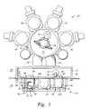
- FIG. 1is a schematic top view of a processing station according to the present invention
- FIG. 2is a schematic perspective view of a cassette for holding substrates
- FIG. 3is a schematic perspective view of a cassette stocker according to the present invention.
- FIG. 4Ais a schematic front view of the cassette stocker of FIG. 3;
- FIG. 4Bis a schematic front view of the cassette stocker of FIG. 4A with a plurality of cassettes
- FIG. 5Ais a schematic side view of the cassette stocker of FIG. 3;
- FIG. 5Bis a schematic side view of the cassette stocker of FIG. 3 with a plurality of cassettes
- FIG. 6is a schematic top view of an end effector located over a docking station
- FIGS. 7A, 7 B and 7 Care schematic perspective views illustrating the end effector of FIG. 6 lifting and moving a cassette
- FIGS. 8A and 8Bare schematic front views of the cassette stocker of FIG. 3 illustrating the path the end effector of FIG. 6 takes in moving a cassette between a loading platform and a cassette docking platform;
- FIG. 9is a schematic perspective view of another embodiment of a cassette stocker having a plurality of vertically disposed docking stations
- FIG. 10is a schematic side view of the cassette stocker of FIG. 9;
- FIG. 11is a schematic side view of the cassette stocker of FIG. 9 with a plurality of cassettes
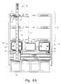
- FIG. 12is a schematic front view of two loading and storage stations connected by an interstation transfer mechanism
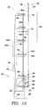
- FIG. 13is a schematic front view of a cassette stocker having a single pair of vertically disposed docking stations.
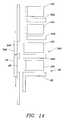
- FIG. 14is a simplified side schematic view of a cassette stocker having a single pair of vertically disposed docking stations, the doors of which open in opposite directions.
- substratebroadly covers any object that is being processed in a semiconductor device processing system.
- substrateincludes, for example, semiconductor wafers, flat panel displays, glass plates or disks, and plastic workpieces.
- FIG. 1is a top view of a processing station 20 of the present invention in which one or more substrates 10 are processed.
- the processing station 20has a front-end staging area 22 which is separated from a loading and storage area 24 by a cleanroom wall 26 .
- Cleanroom wall 26separates a cleanroom 28 , where loading and storage area 24 is located, from a gray area 30 , where a processing system 32 is housed.
- the loading and storage area 24is where cassettes of substrates are delivered and loaded/unloaded into/from the processing station 20 .
- Processing system 32may include one or more load lock chambers 34 , a central transfer chamber 36 , and a plurality of processing chambers 38 .
- processing system and staging area illustrated in FIG. 1are merely representative.
- the processing systemcould have just a single processing chamber, or it could be a device, such as a chemical mechanical polisher, that does not include any processing chambers.
- the processing systemcould include metrology devices instead of or in addition to processing devices.
- one or more substrates 10are brought to the loading and storage area 24 of the processing station in a cassette 100 .
- Substrates 10are supported in cassette 100 in a generally parallel horizontal configuration by slot ridges 102 .
- Substratesmay be loaded and unloaded from cassette 100 through an entry port 103 located in a generally flat front face 106 of the cassette.
- a removable cassette door 104may be secured to entry port 103 to prevent the substrates from being exposed to contaminants when the cassette is moved between processing stations or stored outside a processing station.
- Each cassette 100also includes three cylindrical indentations 108 (shown in phantom and only two of which are visible in FIG. 2) formed in an underside 110 of the cassette.
- cassette 100When cassette 100 is stored at the processing station, three support pins will fit into indentations 108 to support the cassette.
- Two handles 112(only one is shown in this perspective view) which project from sidewalls 114 may be used to manually carry the cassette.
- a generally rectangular flange 116 having an L-shaped cross-sectionprojects from a top surface 118 of the cassette.
- a robotic cassette mover at the processing stationmay manipulate the cassette by means of flange 116 .
- loading and storage area 24 of processing station 20includes a cassette loading platform 52 , two cassette substrate transfer or docking stations 40 located on either side of loading platform 52 , and a cassette stocker or storage stations 50 (only partially illustrated in FIG. 1 so that docking stations 40 may be seen) for storing cassettes at the processing station and moving the cassettes to and from loading platform 52 and docking stations 40 .
- a cassette 100may be placed on or removed from loading platform 52 either manually or by an AGV. From the loading platform 52 , the cassette 100 may be moved to one of docking stations 40 or into cassette stocker 50 .
- Loading platform 52has generally the same perimeter shape as a cassette.
- Three support pins 64project vertically from the loading platform 52 to mate with the indentations in the underside of the cassette 100 and thus to secure the cassette on the loading platform 52 .
- cassettes 100may be positioned at one or both docking stations 40 .
- Each docking station 40includes a docking platform 42 to support a cassette, an opening 46 formed through cleanroom wall 26 , a movable door 44 which seals opening 46 when a substrate is not to be transferred through opening 46 or when a cassette is not positioned on docking platform 42 , and a mechanism to unlock cassette door 104 and retract the door 104 into front-end staging area 22 to provide horizontal access to the substrates stored within the cassette.
- the moveable door 44may behave as a “receiver” and receive the cassette door 104 of a cassette, and then move below the opening 46 (carrying the cassette door 104 ) so as to allow horizontal access through the opening 46 to substrates stored within the cassette.
- a description of the preferred configuration and operation of docking station 40may be found in U.S. patent application Ser. No. 09/012,323, entitled “A Wafer Cassette Load Station”, filed Jan. 23, 1998, by Eric A. Nering, et al., assigned to the assignee of the present invention, the entire disclosure of which is incorporated herein by reference.
- Cassette stocker 50includes a frame 60 that supports one or more storage racks 58 (shown in FIG. 4 A and not illustrated in FIG. 1 so that the docking stations may be shown), and a robotic cassette mover 56 to move the cassettes between the storage rack 58 , the loading platform 52 , and the docking platforms 42 .
- Frame 60may be bolted to the floor of cleanroom 28 and/or secured to the cleanroom wall 26 .
- the frame 60is at least partially disposed below the docking platforms 42 and loading platform 52 so that the footprint of processing station 20 is minimally increased if increased at all.
- Storage rack 58may include a vertical column of support shelves 62 above each of the two docking stations 40 . Each column may include, for example, one, two, three or more individual support shelves 62 .
- storage rack 58 shown in FIGS. 3-5Bprovides storage space for six cassettes 100 in support shelves 62 a - 62 f (see FIG. 4 B).
- Each support shelf, such as support shelf 62 amay be a horizontally oriented plate having substantially the same perimeter shape as the cassette 100 .
- Three support pins 64project vertically from the support shelf 62 and are positioned to mate with receiving indentations 108 in the underside of the cassette 100 .
- Two vertical posts 66may be used to secure the outer edge of each support shelf 62 a - 62 f to frame 60 . Additionally, the support shelves 62 could be secured to the cleanroom wall for additional support.
- Robotic cassette mover 56is used to move cassettes 100 between the storage shelves 62 , the loading platform 52 and the docking platforms 42 .
- the robotic cassette mover 56includes a vertically movable end effector 72 which is attached to a horizontally movable support strut 74 .
- the support strut 74permits arbitrary horizontal movement of end effector 72 in a plane parallel to cleanroom wall 26 .
- the bottom of support strut 74may be secured to a lateral slider 76 which can move horizontally along a horizontal guide 78 that is attached to or formed as part of frame 60 .
- the lateral slider 76may be driven from side-to-side by a horizontal lead screw 80 , which is rotated by a horizontal drive motor 82 .
- the horizontal drive motor 82may be secured to frame 60 .
- end effector 72may be attached to a vertical slider 84 (FIG. 4B) which can slide vertically along a vertical guide 86 (FIG. 5B) attached to or formed as part of support strut 74 .
- the vertical slider 84may be driven up and down by a vertical lead screw 87 (shown in phantom in FIGS. 4A-5B) which may be rotated by a vertical drive motor 88 .
- the vertical drive motormay be supported by lateral slider 76 .
- Horizontal drive motor 82 and vertical drive motor 88may be connected to a control system (not shown), such as a programmable digital computer, to control the vertical and horizontal motion of end effector 72 .
- the actuators which drive the movement of the end effector 72may include stepper motors, pneumatic actuators and other devices known to impart movement in a controllable manner.
- a belt drive assembly or other known mechanismcan be utilized to drive the sliders both vertically and horizontally.
- end effector 72projects horizontally from support strut 74 toward cleanroom wall 26 .
- the end effector 72includes a generally flat, hook-shaped finger 90 that defines a rectangular gap 92 which is open on one side of the end effector 72 .
- the end effector 72is adapted to engage a portion of a cassette 100 through the use of the open end of the end effector 72 .
- end effector 72is vertically positioned between flange 116 and top surface 118 of cassette 100 .
- FIG. 7Bthe end effector 72 is moved laterally so that a base 117 of flange 116 fits into gap 92 .
- end effector 72is moved vertically upward so that an inner rim 94 of the end effector 72 contacts an underside 119 of flange 116 to lift the cassette 100 .
- the end effector 72may then be moved laterally to carry cassette 100 to another support shelf 62 or to the loading platform 52 or to a docking platform 42 .
- a cassette 100may be transported from loading platform 52 to a support shelf, such as support shelf 62 c.
- a cassette 100is loaded onto the loading platform 52 , either manually or by an AGV.
- end effector 72is positioned to the left of the cassette at a vertical height between upper surface 118 of the cassette 100 and the lower surface of flange 116 .
- the support strut 74moves rightwardly until end effector 72 engages the support flange (phantom line A). Then, the end effector 72 moves upwardly to raise the cassette 100 off of the loading platform 52 (phantom line B).
- end effector 72raises the cassette 100 until the cassette 100 is generally aligned above the support shelf 62 c, with sufficient vertical clearance to permit the underside of the cassette 100 to move horizontally over support pins 64 (phantom line C). Then support strut 74 is moved leftwardly to position the cassette 100 over the support shelf 62 c, and the end effector 72 moves downwardly until the cassette 100 rests on support pins 64 (phantom line D).
- the end effector 72may be withdrawn by moving it leftwardly until it clears the flange 116 , and then moving it upwardly and rightwardly between the top of the flange 116 and the bottom of support shelf 62 b (phantom line E).
- end effector 72moves leftwardly between the top of flange 116 and the bottom of support shelf 62 b (phantom line F), downwardly until the end effector 72 is located at a vertical position between the top surface of the cassette 100 and the underside of the flange 116 (phantom line G), and rightwardly until it engages the flange 116 (phantom line H). Then the end effector 72 moves upwardly to lift the cassette 100 off the support plate 62 b and then rightwardly to carry the cassette 100 into the vertical channel between the storage racks 58 (phantom line I). From this position, the cassette 100 may be moved up or down and then left or right to a new storage shelf, to one of the docking platforms 42 , or to the loading platform 52 .
- hook-shaped finger 90 of end effector 72curves to the right so that rectangular gap 92 is open on the right.
- hook-shaped finger 90 curved to the left so that rectangular gap 92 was open on the leftthen the relative lateral motion of the end effector to engage and disengage the cassette 100 would be reversed.
- the end effector 72would be positioned on the right side of the cassette 100 and moved leftwardly to engage the flange 116 .
- a cassette 100is transported to processing station 20 and placed on loading platform 52 , e.g., manually or by an AGV.
- the robotic cassette mover 56transports the cassette from the loading platform 52 to one of the docking stations 40 , which aligns the front face of the cassette 100 with docking station door 44 .
- Docking station door 44then retracts, opening cassette door 104 so that entry port 102 mates with opening 46 in cleanroom wall 26 .
- a wafer handling robot 48 in front-end staging area 22extracts the substrates from the cassette 100 through opening 46 in the cleanroom wall 26 and inserts the substrates into one of the load lock chambers 34 .
- a robot 39 in transfer chamber 36moves substrates between the load lock 34 and the processing chambers 38 .
- wafer handling robot 48extracts the substrate from one of the lock load chambers 34 , and returns the substrate to cassette 100 through opening 46 in cleanroom wall 26 .
- cassette door 104is closed, the cassette 100 is moved to storage rack 58 or loading platform 52 , and a new cassette 100 containing unprocessed substrates is loaded onto the docking station 40 .
- Metrology stationstypically sample and test processed and/or unprocessed wafers stored within the wafer cassettes 100 .
- a metrology stationmay test as few as one wafer within each wafer cassette 100 selected for metrology, the cassette 100 being selected randomly or based on some pre-determined selection criteria according to standard metrology principles. Accordingly, each wafer cassette 100 presented for metrology may have significantly less resident time at a particular docking station 40 operated in connection with a metrology station than if the wafer cassette 100 were presented for processing in a processing station.
- the time required to open and close the doors and the time required to move a first cassette 100 from the docking station 40 and replace the first cassette 100 with a second cassette 100may result in undesirable downtime of the metrology station if only one or two docking stations 40 are employed. Further, certain processing stations, particularly those with short processing times, may also have unnecessary downtime as a result of using only one or two docking stations 40 .
- FIGS. 9-11illustrate a stacked docking station embodiment of a loading and storage area 24 of processing station 20 having two lower substrate docking stations 40 and two upper substrate docking stations 540 .
- the loading and storage area 24 of processing station 20includes a cassette loading platform 52 , two lower cassette docking or substrate transfer stations 40 located on either side of loading platform 52 , and cassette stocker or storage stations 50 for storing cassettes 100 at the processing station and moving the cassettes 100 to and from loading platform 52 and docking stations 40 .
- This embodimentalso includes two upper cassette docking or substrate transfer stations 540 each of which is located above one of the docking stations 40 .
- the docking stationsthus at least partially overlap, and preferably completely overlap, in footprint.
- the vertically disposed docking stationsare also vertically disposed relative to one or (preferably) more of the support shelves 62 .
- a cassette 100may be placed onto or removed from loading platform 52 either manually or by an AGV.
- cassettes 100may be positioned at one of the lower docking stations 40 or also at one of the upper docking stations 540 .
- Each lower docking station 40includes a lower docking platform 42 to support a cassette 100 , a lower opening 46 formed through cleanroom wall 26 , a lower movable door 44 which seals lower opening 46 when a substrate is not to be transferred through lower opening 46 or when a cassette 100 is not positioned on lower docking platform 42 , and a mechanism to unlock cassette door 104 and retract the door 104 into front-end staging area 22 so as to provide horizontal access to the substrate.
- Each upper docking station 540likewise includes an upper docking platform 542 to support a cassette, an opening 546 formed through cleanroom wall 26 , an upper movable door 544 which seals upper opening 546 when a substrate is not to be transferred through upper opening 546 or when a cassette 100 is not positioned on upper docking platform 542 , and a mechanism to unlock cassette door 104 and retract the door 104 into front-end staging area 22 to provide horizontal access to the substrate.
- Upper docking station 540is of similar construction and operation as lower docking station 40 .
- upper movable door 544is of similar construction and operation as lower movable door 44 . Suitable space is provided between upper opening 546 and lower opening 46 so that downward movement of the upper movable door 544 does not interfere with the operation of lower movable door 44 as will be readily appreciated by one of ordinary skill in the art.
- upper movable door 544could be arranged to open upwardly allowing the two doors 44 , 544 and the two docking stations 540 , 40 to be located closer together (as shown in FIG. 14 ).
- the embodiment described hereinhas an upper and lower docking station 40 , 540 associated with each of the storage racks 58 .
- a plurality of upper docking stations 540may be used limited only by available vertical space.
- the upper docking station 540 and the lower docking station 40may be separated by one or more of the support shelves 62 , or both the upper and lower docking stations may be positioned above one or more of the plurality of storage shelves 62 .
- the embodiment described abovealso includes two storage racks 58 disposed above two pairs of docking stations 40 , 540 and a loading station 52 disposed between the two docking stations.
- FIG. 9is a perspective view of one embodiment of the invention having two pairs of docking stations 40 , 540 and three storage shelves 62 a-c or 62 d-f disposed above each of the pair of docking stations 40 , 540 . While three support shelves 62 a-c or 62 d-f are shown, only one support shelf 62 a or 62 d could also be used advantageously. Components which form a part of the earlier described embodiments are identified using the same reference numerals.
- FIGS. 10 and 11further depict docking stations 40 , 540 and storage shelves 62 a-c in a side view, shown with and without cassettes, respectively. Referring to FIG.
- an interstation transfer apparatus 120may be used to move cassettes 100 between adjacent processing stations 20 ′ and 20 ′′, thereby eliminating the need for AGVs or manual transport.
- Interstation transfer apparatus 120includes an overhead support beam 122 which may be secured to posts 66 ′ and 66 ′′ of adjacent cassette stockers 50 ′ and 50 ′′.
- a transfer arm 124may be attached to a slider 126 that moves horizontally along a guide 127 that is attached to or formed as part of support beam 122 .
- the slider 126may be moved horizontally by a lead screw 130 which may be rotated by a horizontal drive motor 132 .
- An end effector 128may be connected to transfer arm 124 by a pneumatic actuator 134 to provide end effector 128 with a short vertical stroke.
- the cassette 100is moved by robotic cassette mover 56 ′ to the upper right-hand support shelf, i.e., support shelf 62 d ′, of cassette stocker 50 ′.
- End effector 128moves horizontally over flange 116 , then down to a vertical position between the bottom of the flange and the top of the cassette. Then the end effector 128 moves to the right until it engages the cassette flange 116 .
- End effector 128lifts the cassette 100 off support plate 62 d ′, and horizontal drive motor 132 drives the transfer arm 124 rightwardly until the cassette 100 is located over the upper left-hand support shelf 62 a ′′ of cassette stocker 50 ′′. Finally, the end effector 128 lowers the cassette 100 onto support shelf 62 a ′′ and withdraws.
- Interstation transfer apparatus 120provides an extremely simple method of transferring cassettes 100 between adjacent processing stations 20 ′, 20 ′′. This may be particularly useful where one of the processing stations is a metrology station (which could be located entirely inside the cleanroom 28 ), since it permits the metrology measurements to be made without building a metrology apparatus into the processing equipment 20 ′, 20 ′′ and without using a factory automation system 22 .
- cassette stockers 50 ′ and 50 ′′are illustrated as positioned against the same cleanroom wall 26
- the interstation transfer apparatus 120could include rotary mechanisms to allow handoff between end effectors 128 on different support beams. This would permit processing stations 20 ′ and 20 ′′ to be positioned around the corners or at opposite walls of the cleanroom.
- the embodiments described aboveinclude two storage racks 58 , each disposed above docking stations 40 , 540 and a loading station 52 disposed between the two storage racks 58 .
- FIGS. 13 and 14are front views of cassette stockers having a single pair of docking stations 40 , 540 and two storage shelves 62 a-b disposed above the docking stations 40 , 540 .
- the upper moveable door 544opens downwardly in FIG. 13, and upwardly in FIG. 14 .
- the two docking stations 540 , 40can be located closer together so as to reduce the overall height of the cassette stocker.
- support shelf 62 ais shown in phantom to indicate that only one support shelf 62 b could be advantageously used.
- An enclosure 550is disposed about the docking stations 40 , 540 , the loading station 52 and the cassette support shelves 62 . Components which form a part of the earlier described embodiments are identified using the same numbers.
- Substratesmay be loaded into the system 20 at either a docking station 40 , 540 position, at any one of the storage shelf positions 62 or at a loading station 52 .
- the loading station 52could be disposed adjacent either a support shelf 62 or a docking station 40 , 540 .
- the substrate mover system described above with reference to the other embodimentsis utilized with the single stack embodiment of FIG. 13 and operates in the same manner except that support shelves 62 disposed in a single stack eliminate the transfer sequence from the additional stack.
- Each of the embodiments described hereinutilizes available space above or below docking stations, thereby increasing the storage capability of the system without increasing the footprint (area occupied by the system measured in terms of floor space) of the system.
- the storage shelves shown hereinare located above the pair of docking stations, it will be understood that one or more storage shelves could be located below, or between the plurality of vertically disposed docking stations.
- a processing systemcould utilize any configuration of the storage device of the present invention including cassette support shelves disposed adjacent a docking station.
- a vertically arranged pair of docking stationsis preferably associated with each stack of one or more support shelves, a pair of horizontally disposed docking stations may be associated with each stack of support shelves.
- each docking stationis coupled to a separate tool.
- the separate toolsare preferably high throughput tools (metrology tools, etc.).
- a cassette moveris also disposed in proximity to the support shelves and the docking station to effect transfer of cassettes between the support shelves and the docking stations.
Landscapes
- Engineering & Computer Science (AREA)
- Physics & Mathematics (AREA)
- Condensed Matter Physics & Semiconductors (AREA)
- General Physics & Mathematics (AREA)
- Manufacturing & Machinery (AREA)
- Computer Hardware Design (AREA)
- Microelectronics & Electronic Packaging (AREA)
- Power Engineering (AREA)
- Robotics (AREA)
- Container, Conveyance, Adherence, Positioning, Of Wafer (AREA)
- Warehouses Or Storage Devices (AREA)
Abstract
Description
The present invention relates generally to substrate processing, and more particularly to an apparatus for storing and moving substrate cassettes.
Semiconductor devices are made on substrates, such as silicon wafers or glass plates, for use in computers, monitors, and the like. These devices are made by a sequence of fabrication steps, such as thin film deposition, oxidation or nitration, etching, polishing, and thermal and lithographic processing. Although multiple fabrication steps may be performed in a single processing station, substrates must be transported between different processing stations for at least some of the fabrication steps. In addition, random substrates in a particular batch may be tested using metrology devices which require additional stations. Substrates are stored in cassettes for transfer between processing stations, metrology stations and other locations. Although cassettes may be carried manually between processing stations, the transfer of cassettes is typically automated. For example, a cassette may be transported to a processing station in an automatic guided vehicle (AGV), and then loaded from the AGV onto a loading platform in the processing station by a robot. Another robot may extract a substrate from the cassette and transport it into a processing chamber at the processing station. When the fabrication steps are complete, the substrate is loaded back into the cassette. Once all of the substrates have been processed and returned to the cassette, the cassette is removed from the loading platform and transported to another location by the AGV.
In order to ensure that the processing equipment does not sit idle, a nearly continuous supply of unprocessed substrates should be available at the processing station. Unfortunately, many processing stations can hold only a single cassette at the loading platform. Therefore, once all of the substrates in the cassette have been processed, the cassette must be quickly replaced, either manually or by an AGV, with a new cassette containing unprocessed substrates. Running such a just-in-time cassette inventory system requires either significant operator oversight or a large number of AGVs, thereby increasing the costs of the fabrication facility.
Therefore, there is a need for a method and apparatus which continuously supplies substrate cassettes to a processing system so that system down time is reduced or eliminated.
The present invention provides a method and apparatus for storing multiple cassettes at a processing station, ensuring that a nearly continuous supply of unprocessed substrates is available for processing and that the processing equipment does not idle. Multiple cassettes can be stored at a processing station in a front end support frame and a cassette can be moved to one of a plurality of vertically disposed docking stations where substrates are extracted and transferred to the processing equipment. An automation system is mounted or otherwise disposed on the frame to transfer cassettes between docking stations or between processing stations. In another aspect of the invention, cassettes can be transported between different processing stations without the use of an AGV.
In one aspect of the invention, an apparatus is provided which includes a front end frame having a plurality of vertically disposed docking stations and multiple cassette storage stations. An automated transfer assembly is preferably disposed adjacent the docking stations and the storage stations to move cassettes between the storage stations and the docking stations. Additionally, an automated transfer assembly can be located between processing stations to transfer cassettes between processing stations without the need for manual or AGV assistance. In another aspect of the invention, a method is provided for delivering a continuous supply of cassettes to a processing system. The method preferably includes providing a plurality of vertically disposed docking stations and multiple storage stations and moving cassettes between the storage stations and the transfer stations to ensure that substrates are continually supplied to the processing system. Additionally, a method is provided for transferring cassettes between processing stations to continue the processing sequence without the need for manual or AGV assistance.
Other objects, features and advantages of the present invention will become more fully apparent from the following detailed description of the preferred embodiments, the appended claims and the accompanying drawings.
FIG. 1 is a schematic top view of a processing station according to the present invention;
FIG. 2 is a schematic perspective view of a cassette for holding substrates;
FIG. 3 is a schematic perspective view of a cassette stocker according to the present invention;
FIG. 4A is a schematic front view of the cassette stocker of FIG. 3;
FIG. 4B is a schematic front view of the cassette stocker of FIG. 4A with a plurality of cassettes;
FIG. 5A is a schematic side view of the cassette stocker of FIG. 3;
FIG. 5B is a schematic side view of the cassette stocker of FIG. 3 with a plurality of cassettes;
FIG. 6 is a schematic top view of an end effector located over a docking station;
FIGS. 7A,7B and7C are schematic perspective views illustrating the end effector of FIG. 6 lifting and moving a cassette;
FIGS. 8A and 8B are schematic front views of the cassette stocker of FIG. 3 illustrating the path the end effector of FIG. 6 takes in moving a cassette between a loading platform and a cassette docking platform;
FIG. 9 is a schematic perspective view of another embodiment of a cassette stocker having a plurality of vertically disposed docking stations;
FIG. 10 is a schematic side view of the cassette stocker of FIG. 9;
FIG. 11 is a schematic side view of the cassette stocker of FIG. 9 with a plurality of cassettes;
FIG. 12 is a schematic front view of two loading and storage stations connected by an interstation transfer mechanism;
FIG. 13 is a schematic front view of a cassette stocker having a single pair of vertically disposed docking stations; and
FIG. 14 is a simplified side schematic view of a cassette stocker having a single pair of vertically disposed docking stations, the doors of which open in opposite directions.
In the following description, the term “substrate” broadly covers any object that is being processed in a semiconductor device processing system. The term “substrate” includes, for example, semiconductor wafers, flat panel displays, glass plates or disks, and plastic workpieces.
FIG. 1 is a top view of aprocessing station 20 of the present invention in which one ormore substrates 10 are processed. Theprocessing station 20 has a front-end staging area 22 which is separated from a loading andstorage area 24 by acleanroom wall 26.Cleanroom wall 26 separates acleanroom 28, where loading andstorage area 24 is located, from agray area 30, where aprocessing system 32 is housed. The loading andstorage area 24 is where cassettes of substrates are delivered and loaded/unloaded into/from theprocessing station 20.Processing system 32 may include one or moreload lock chambers 34, acentral transfer chamber 36, and a plurality ofprocessing chambers 38. Insideprocessing chambers 38 the substrate may be subjected to a variety of fabrication steps, such as thin film deposition, oxidation, nitration, etching, thermal processing or lithographic processing. The processing system and staging area illustrated in FIG. 1 are merely representative. The processing system could have just a single processing chamber, or it could be a device, such as a chemical mechanical polisher, that does not include any processing chambers. In addition, the processing system could include metrology devices instead of or in addition to processing devices.
Referring to FIGS. 1 and 2, one ormore substrates 10 are brought to the loading andstorage area 24 of the processing station in acassette 100.Substrates 10 are supported incassette 100 in a generally parallel horizontal configuration byslot ridges 102. Substrates may be loaded and unloaded fromcassette 100 through anentry port 103 located in a generally flatfront face 106 of the cassette. Aremovable cassette door 104 may be secured toentry port 103 to prevent the substrates from being exposed to contaminants when the cassette is moved between processing stations or stored outside a processing station. Eachcassette 100 also includes three cylindrical indentations108 (shown in phantom and only two of which are visible in FIG. 2) formed in anunderside 110 of the cassette. Whencassette 100 is stored at the processing station, three support pins will fit intoindentations 108 to support the cassette. Two handles112 (only one is shown in this perspective view) which project fromsidewalls 114 may be used to manually carry the cassette. A generallyrectangular flange 116 having an L-shaped cross-section projects from atop surface 118 of the cassette. As discussed below, a robotic cassette mover at the processing station may manipulate the cassette by means offlange 116.
Referring to FIGS. 1-5B, loading andstorage area 24 ofprocessing station 20 includes acassette loading platform 52, two cassette substrate transfer ordocking stations 40 located on either side ofloading platform 52, and a cassette stocker or storage stations50 (only partially illustrated in FIG. 1 so thatdocking stations 40 may be seen) for storing cassettes at the processing station and moving the cassettes to and fromloading platform 52 anddocking stations 40.
Acassette 100 may be placed on or removed fromloading platform 52 either manually or by an AGV. From theloading platform 52, thecassette 100 may be moved to one ofdocking stations 40 or intocassette stocker 50.Loading platform 52 has generally the same perimeter shape as a cassette. Three support pins64 (only two are shown in the side view of FIG. 5A) project vertically from theloading platform 52 to mate with the indentations in the underside of thecassette 100 and thus to secure the cassette on theloading platform 52.
To transfer substrates through thecleanroom wall 26, cassettes100 (shown in phantom in FIG. 1) may be positioned at one or bothdocking stations 40. Eachdocking station 40 includes adocking platform 42 to support a cassette, anopening 46 formed throughcleanroom wall 26, amovable door 44 which sealsopening 46 when a substrate is not to be transferred throughopening 46 or when a cassette is not positioned on dockingplatform 42, and a mechanism to unlockcassette door 104 and retract thedoor 104 into front-end staging area 22 to provide horizontal access to the substrates stored within the cassette. For example, themoveable door 44 may behave as a “receiver” and receive thecassette door 104 of a cassette, and then move below the opening46 (carrying the cassette door104) so as to allow horizontal access through theopening 46 to substrates stored within the cassette. A description of the preferred configuration and operation ofdocking station 40 may be found in U.S. patent application Ser. No. 09/012,323, entitled “A Wafer Cassette Load Station”, filed Jan. 23, 1998, by Eric A. Nering, et al., assigned to the assignee of the present invention, the entire disclosure of which is incorporated herein by reference.
Referring to FIGS. 6-7A,end effector 72 projects horizontally fromsupport strut 74 towardcleanroom wall 26. Theend effector 72 includes a generally flat, hook-shapedfinger 90 that defines arectangular gap 92 which is open on one side of theend effector 72. Theend effector 72 is adapted to engage a portion of acassette 100 through the use of the open end of theend effector 72. In order to transportcassette 100,end effector 72 is vertically positioned betweenflange 116 andtop surface 118 ofcassette 100. Referring to FIG. 7B, theend effector 72 is moved laterally so that abase 117 offlange 116 fits intogap 92. Finally, referring to FIG. 7C,end effector 72 is moved vertically upward so that aninner rim 94 of theend effector 72 contacts anunderside 119 offlange 116 to lift thecassette 100. Theend effector 72 may then be moved laterally to carrycassette 100 to another support shelf62 or to theloading platform 52 or to adocking platform 42.
Referring to FIGS. 7A-8A, acassette 100 may be transported fromloading platform 52 to a support shelf, such assupport shelf 62c. Withsupport strut 74 positioned to the side ofloading platform 52, acassette 100 is loaded onto theloading platform 52, either manually or by an AGV. To lift thecassette 100 offloading platform 52,end effector 72 is positioned to the left of the cassette at a vertical height betweenupper surface 118 of thecassette 100 and the lower surface offlange 116. Thesupport strut 74 moves rightwardly untilend effector 72 engages the support flange (phantom line A). Then, theend effector 72 moves upwardly to raise thecassette 100 off of the loading platform52 (phantom line B). To move thecassette 100 to one of the support shelves, e.g.,support shelf 62c,end effector 72 raises thecassette 100 until thecassette 100 is generally aligned above thesupport shelf 62c,with sufficient vertical clearance to permit the underside of thecassette 100 to move horizontally over support pins64 (phantom line C). Then supportstrut 74 is moved leftwardly to position thecassette 100 over thesupport shelf 62c,and theend effector 72 moves downwardly until thecassette 100 rests on support pins64 (phantom line D). Theend effector 72 may be withdrawn by moving it leftwardly until it clears theflange 116, and then moving it upwardly and rightwardly between the top of theflange 116 and the bottom ofsupport shelf 62b(phantom line E).
Referring to FIG. 8B, in order to remove thecassette 100 fromsupport shelf 62c,these steps are generally repeated in reverse order. Specifically,end effector 72 moves leftwardly between the top offlange 116 and the bottom ofsupport shelf 62b(phantom line F), downwardly until theend effector 72 is located at a vertical position between the top surface of thecassette 100 and the underside of the flange116 (phantom line G), and rightwardly until it engages the flange116 (phantom line H). Then theend effector 72 moves upwardly to lift thecassette 100 off thesupport plate 62band then rightwardly to carry thecassette 100 into the vertical channel between the storage racks58 (phantom line I). From this position, thecassette 100 may be moved up or down and then left or right to a new storage shelf, to one of thedocking platforms 42, or to theloading platform 52.
In the embodiments described in FIGS. 7A-8B, hook-shapedfinger 90 ofend effector 72 curves to the right so thatrectangular gap 92 is open on the right. Of course, if hook-shapedfinger 90 curved to the left so thatrectangular gap 92 was open on the left, then the relative lateral motion of the end effector to engage and disengage thecassette 100 would be reversed. For example, to lift thecassette 100 from asupport shelf 62b,theend effector 72 would be positioned on the right side of thecassette 100 and moved leftwardly to engage theflange 116.
Referring to FIGS. 1-3, in operation acassette 100 is transported toprocessing station 20 and placed onloading platform 52, e.g., manually or by an AGV. Therobotic cassette mover 56 transports the cassette from theloading platform 52 to one of thedocking stations 40, which aligns the front face of thecassette 100 withdocking station door 44.Docking station door 44 then retracts, openingcassette door 104 so thatentry port 102 mates with opening46 incleanroom wall 26. Awafer handling robot 48 in front-end staging area 22 extracts the substrates from thecassette 100 through opening46 in thecleanroom wall 26 and inserts the substrates into one of theload lock chambers 34. Arobot 39 intransfer chamber 36 moves substrates between theload lock 34 and theprocessing chambers 38. When the fabrication steps are complete,wafer handling robot 48 extracts the substrate from one of thelock load chambers 34, and returns the substrate tocassette 100 through opening46 incleanroom wall 26. Once all of the substrates have been processed,cassette door 104 is closed, thecassette 100 is moved tostorage rack 58 orloading platform 52, and anew cassette 100 containing unprocessed substrates is loaded onto thedocking station 40.
As stated above, the processing system could perform inspection processes using metrology devices instead of or in addition to fabrication steps. Metrology stations typically sample and test processed and/or unprocessed wafers stored within thewafer cassettes 100. Typically, a metrology station may test as few as one wafer within eachwafer cassette 100 selected for metrology, thecassette 100 being selected randomly or based on some pre-determined selection criteria according to standard metrology principles. Accordingly, eachwafer cassette 100 presented for metrology may have significantly less resident time at aparticular docking station 40 operated in connection with a metrology station than if thewafer cassette 100 were presented for processing in a processing station. As a result, the time required to open and close the doors and the time required to move afirst cassette 100 from thedocking station 40 and replace thefirst cassette 100 with asecond cassette 100 may result in undesirable downtime of the metrology station if only one or twodocking stations 40 are employed. Further, certain processing stations, particularly those with short processing times, may also have unnecessary downtime as a result of using only one or twodocking stations 40.
Therefore, it may be desirable to incorporate a plurality of vertically stacked docking stations in connection with eachstorage rack 58. FIGS. 9-11 illustrate a stacked docking station embodiment of a loading andstorage area 24 ofprocessing station 20 having two lowersubstrate docking stations 40 and two uppersubstrate docking stations 540. As in the previous embodiments, the loading andstorage area 24 ofprocessing station 20 includes acassette loading platform 52, two lower cassette docking orsubstrate transfer stations 40 located on either side ofloading platform 52, and cassette stocker orstorage stations 50 for storingcassettes 100 at the processing station and moving thecassettes 100 to and fromloading platform 52 anddocking stations 40. This embodiment, however, also includes two upper cassette docking orsubstrate transfer stations 540 each of which is located above one of thedocking stations 40. The docking stations thus at least partially overlap, and preferably completely overlap, in footprint. The vertically disposed docking stations are also vertically disposed relative to one or (preferably) more of the support shelves62.
According to this embodiment, acassette 100 may be placed onto or removed fromloading platform 52 either manually or by an AGV. To transfer substrates through thecleanroom wall 26,cassettes 100 may be positioned at one of thelower docking stations 40 or also at one of theupper docking stations 540. Eachlower docking station 40 includes alower docking platform 42 to support acassette 100, alower opening 46 formed throughcleanroom wall 26, a lowermovable door 44 which sealslower opening 46 when a substrate is not to be transferred throughlower opening 46 or when acassette 100 is not positioned onlower docking platform 42, and a mechanism to unlockcassette door 104 and retract thedoor 104 into front-end staging area 22 so as to provide horizontal access to the substrate. Eachupper docking station 540 likewise includes anupper docking platform 542 to support a cassette, anopening 546 formed throughcleanroom wall 26, an uppermovable door 544 which sealsupper opening 546 when a substrate is not to be transferred throughupper opening 546 or when acassette 100 is not positioned onupper docking platform 542, and a mechanism to unlockcassette door 104 and retract thedoor 104 into front-end staging area 22 to provide horizontal access to the substrate.
The embodiment described above also includes twostorage racks 58 disposed above two pairs ofdocking stations loading station 52 disposed between the two docking stations. Preferably, six cassette support shelves62a-fare disposed above thedocking stations docking stations docking stations
FIG. 9 is a perspective view of one embodiment of the invention having two pairs ofdocking stations docking stations support shelf docking stations interstation transfer apparatus 120 may be used to movecassettes 100 betweenadjacent processing stations 20′ and20″, thereby eliminating the need for AGVs or manual transport.Interstation transfer apparatus 120 includes anoverhead support beam 122 which may be secured toposts 66′ and66″ ofadjacent cassette stockers 50′ and50″. Atransfer arm 124 may be attached to aslider 126 that moves horizontally along aguide 127 that is attached to or formed as part ofsupport beam 122. Theslider 126 may be moved horizontally by alead screw 130 which may be rotated by ahorizontal drive motor 132. Anend effector 128 may be connected to transferarm 124 by apneumatic actuator 134 to provideend effector 128 with a short vertical stroke.
In order to transport thecassettes 100 betweenadjacent processing stations 20′,20″, thecassette 100 is moved byrobotic cassette mover 56′ to the upper right-hand support shelf, i.e.,support shelf 62d′, ofcassette stocker 50′.End effector 128 moves horizontally overflange 116, then down to a vertical position between the bottom of the flange and the top of the cassette. Then theend effector 128 moves to the right until it engages thecassette flange 116.End effector 128 lifts thecassette 100 offsupport plate 62d′, andhorizontal drive motor 132 drives thetransfer arm 124 rightwardly until thecassette 100 is located over the upper left-hand support shelf 62a″ ofcassette stocker 50″. Finally, theend effector 128 lowers thecassette 100 ontosupport shelf 62a″ and withdraws.
Althoughcassette stockers 50′ and50″ are illustrated as positioned against thesame cleanroom wall 26, theinterstation transfer apparatus 120 could include rotary mechanisms to allow handoff betweenend effectors 128 on different support beams. This would permitprocessing stations 20′ and20″ to be positioned around the corners or at opposite walls of the cleanroom.
The embodiments described above include twostorage racks 58, each disposed abovedocking stations loading station 52 disposed between the two storage racks58. Preferably, six cassette support shelves62a-fare disposed above each of the one or more docking stations. While this configuration is believed to provide the highest throughput of substrates in the available space, the invention also includes a single pair ofdocking stations docking stations docking stations docking stations moveable door 544 opens downwardly in FIG. 13, and upwardly in FIG.14. When theupper door 544 opens upwardly as shown in FIG. 14, the twodocking stations support shelf 62ais shown in phantom to indicate that only onesupport shelf 62bcould be advantageously used. Anenclosure 550 is disposed about thedocking stations loading station 52 and the cassette support shelves62. Components which form a part of the earlier described embodiments are identified using the same numbers.
Substrates may be loaded into thesystem 20 at either adocking station loading station 52. Theloading station 52 could be disposed adjacent either a support shelf62 or adocking station
Each of the embodiments described herein utilizes available space above or below docking stations, thereby increasing the storage capability of the system without increasing the footprint (area occupied by the system measured in terms of floor space) of the system. Although the storage shelves shown herein are located above the pair of docking stations, it will be understood that one or more storage shelves could be located below, or between the plurality of vertically disposed docking stations. Accordingly, a processing system could utilize any configuration of the storage device of the present invention including cassette support shelves disposed adjacent a docking station. Further, although a vertically arranged pair of docking stations is preferably associated with each stack of one or more support shelves, a pair of horizontally disposed docking stations may be associated with each stack of support shelves. In such a horizontal configuration each docking station is coupled to a separate tool. The separate tools are preferably high throughput tools (metrology tools, etc.). Preferably, a cassette mover is also disposed in proximity to the support shelves and the docking station to effect transfer of cassettes between the support shelves and the docking stations. Accordingly, while the present invention has been disclosed in connection with the preferred embodiments thereof, it should be understood that other embodiments may fall within the spirit and scope of the invention, as defined by the following claims.
Claims (20)
1. An apparatus for storing cassettes, comprising:
two or more vertically disposed docking stations, each docking station including structure adapted to support a cassette;
a first plurality of cassette storage shelves arranged in a vertical column positioned vertically relative to the docking stations;
a second plurality of cassette storage shelves arranged in a vertical column and separated by a vertical channel from the first plurality of cassette storage shelves, the vertical channel being sized to permit movement of a cassette therethrough in a vertical direction;
structure adapted to support the first and second pluralities of cassette storage shelves;
a loading platform positioned vertically below the vertical channel;
a cassette mover having a support member positioned adjacent the shelves and movable in a path generally parallel to the shelves to carry a cassette between the shelves and the two or more docking stations, the cassette mover including a mechanism adapted to impart movement to the cassette mover; and
an end effector movably connected to the support member and configured to engage a cassette by moving in at least one of a horizontal direction and a vertical direction.
2. The apparatus ofclaim 1 , wherein the shelves are configured to be positioned adjacent a cleanroom wall.
3. The apparatus ofclaim 2 , wherein one or more of the shelves are positioned above the two or more docking stations.
4. The apparatus ofclaim 1 , further comprising a frame supporting the cassette storage shelves and the support member.
5. The apparatus ofclaim 4 , wherein the frame substantially fits below the two or more docking stations.
6. The apparatus ofclaim 1 , further comprising a frame positioned substantially below the two or more docking stations wherein a lower end of the support member is slidably connected to the frame.
7. The apparatus ofclaim 6 , further comprising a vertical guide joined to the support member and a first slider which slidably engages the vertical guide, wherein the end effector is joined to the first slider.
8. The apparatus ofclaim 7 , further comprising a horizontal guide joined to the frame and a second slider which slidably engages the horizontal guide, wherein the support member is joined to the second slider.
9. The apparatus ofclaim 8 , further comprising a first lead screw engaging the first slider and a first drive motor adapted to rotate the first lead screw so as to drive the first slider along the first guide to move the end effector vertically.
10. The apparatus ofclaim 9 , further comprising a second lead screw engaging the second slider and a second drive motor adapted to rotate the second lead screw and drive the second slider along the second guide to move the support member and the end effector horizontally.
11. The apparatus ofclaim 1 , wherein the end effector includes a hook-shaped finger adapted to engage a bottom surface of a flange on a top of a cassette.
12. The apparatus ofclaim 1 , wherein each shelf includes a plurality of pins that project vertically from the shelf to engage corresponding indentations in the underside of a cassette positioned on the shelf.
13. An apparatus for storing cassettes, comprising:
a first plurality of cassette storage shelves positioned adjacent a wall and arranged in a vertical column positioned vertically above a plurality of vertically disposed cassette docking stations, each docking station including structure adapted to support a cassette;
a second plurality of cassette storage shelves arranged in a vertical column and separated by a vertical channel from the first plurality of cassette storage shelves, the vertical channel being sized to permit movement of a cassette therethrough in a vertical direction;
structure adapted to support the first and second pluralities of cassette storage shelves;
a loading platform positioned vertically below the vertical channel; and
a cassette mover adapted to carry a cassette between the shelves and the docking stations, the cassette mover including a support member positioned adjacent the shelves and movable in a plane parallel to the wall, a mechanism adapted to impart movement to the cassette mover, and an end effector configured to engage a cassette by moving in at least one of a horizontal direction and a vertical direction, the end effector slidably connected to the support member.
14. The apparatus ofclaim 13 , wherein the cassette mover is configured to transport a cassette to a selected support shelf by moving the cassette vertically through the channel to position the cassette substantially adjacent and at a higher elevation than the selected support shelf, and then horizontally to position the cassette over the selected support shelf.
15. The apparatus ofclaim 1 wherein an upper one of the vertically disposed docking stations comprises a door adapted to open upwardly, and
a lower one of the vertically disposed docking stations comprises a door adapted to open downwardly.
16. An apparatus for storing cassettes, comprising:
a first plurality of vertically disposed docking stations, the docking stations of the first plurality each including structure adapted to support a cassette;
a second plurality of vertically disposed docking stations, the docking stations of the second plurality each including structure adapted to support a cassette;
a first plurality of cassette storage shelves arranged in a vertical column positioned vertically relative to the first plurality of docking stations;
a second plurality of cassette storage shelves arranged in a vertical column positioned vertically relative to the second plurality of docking stations;
structure adapted to support the first and second pluralities of cassette storage shelves;
a cassette mover to carry a cassette between the shelves and the docking stations, the cassette mover having
a support member disposed adjacent the shelves and movable in a path generally parallel to the shelves, the cassette mover including a mechanism adapted to impart movement to the cassette mover; and
an end effector movably connected to the support member and configured to engage a cassette by moving in at least one of a horizontal direction and a vertical direction.
17. The apparatus ofclaim 16 , wherein the first and second pluralities of docking stations are separated by a vertical channel that is sized to permit movement of a cassette therethrough in a vertical direction.
18. The apparatus ofclaim 17 , further comprising a loading platform positioned vertically below the vertical channel.
19. An apparatus for storing cassettes, comprising:
a plurality of vertically disposed cassette docking stations, each docking station including structure adapted to support a cassette;
a plurality of cassette storage shelves positioned adjacent a wall and arranged in a vertical column positioned vertically above the docking stations;
structure adapted to support the plurality of cassette storage shelves; and
a cassette mover adapted to carry a cassette between the shelves and the docking stations, the cassette mover including a support member positioned adjacent the shelves and movable in a plane parallel to the wall, a mechanism adapted to impart movement to the cassette mover, and an end effector configured to engage a cassette by moving in at least one of a horizontal direction and a vertical direction, the end effector slidably connected to the support member;
wherein an upper one of the vertically disposed docking stations comprises a door adapted to open upwardly, and a lower one of the vertically disposed docking stations comprises a door adapted to open downwardly.
20. An apparatus for storing cassettes, comprising:
a first plurality of vertically disposed docking stations, the docking stations of the first plurality each including structure adapted to support a cassette;
a second plurality of vertically disposed docking stations, the docking stations of the second plurality each including structure adapted to support a cassette;
a first cassette storage shelf positioned vertically above the first plurality of docking stations;
a second cassette storage shelf positioned vertically above the second plurality of docking stations;
structure adapted to support the first and second pluralities of cassette storage shelves;
a cassette mover to carry a cassette between the shelves and the docking stations, the cassette mover having a support member disposed adjacent the shelves and movable in a path generally parallel to the shelves, the cassette mover including a mechanism adapted to impart movement to the cassette mover; and
an end effector movably connected to the support member and configured to engage a cassette by moving in at least one of a horizontal direction and a vertical direction.
Priority Applications (9)
| Application Number | Priority Date | Filing Date | Title |
|---|---|---|---|
| US09/527,092US6506009B1 (en) | 2000-03-16 | 2000-03-16 | Apparatus for storing and moving a cassette |
| TW090100799ATW504732B (en) | 2000-03-16 | 2001-01-12 | Apparatus for storing and moving a cassette |
| EP01104511AEP1134641B1 (en) | 2000-03-16 | 2001-03-02 | Apparatus for storing and moving a cassette |
| DE60100575TDE60100575T2 (en) | 2000-03-16 | 2001-03-02 | Device for storing and moving a cassette |
| KR1020010013692AKR100905565B1 (en) | 2000-03-16 | 2001-03-16 | Apparatus for storing and moving a cassette |
| JP2001076334AJP4919539B2 (en) | 2000-03-16 | 2001-03-16 | Cassette storage apparatus, semiconductor processing station, and operation method thereof |
| US10/263,163US6955517B2 (en) | 2000-03-16 | 2002-10-02 | Apparatus for storing and moving a cassette |
| US11/248,375US7234908B2 (en) | 2000-03-16 | 2005-10-11 | Apparatus for storing and moving a cassette |
| US11/766,093US20070237609A1 (en) | 2000-03-16 | 2007-06-20 | Apparatus for storing and moving a cassette |
Applications Claiming Priority (1)
| Application Number | Priority Date | Filing Date | Title |
|---|---|---|---|
| US09/527,092US6506009B1 (en) | 2000-03-16 | 2000-03-16 | Apparatus for storing and moving a cassette |
Related Child Applications (1)
| Application Number | Title | Priority Date | Filing Date |
|---|---|---|---|
| US10/263,163DivisionUS6955517B2 (en) | 2000-03-16 | 2002-10-02 | Apparatus for storing and moving a cassette |
Publications (1)
| Publication Number | Publication Date |
|---|---|
| US6506009B1true US6506009B1 (en) | 2003-01-14 |
Family
ID=24100060
Family Applications (4)
| Application Number | Title | Priority Date | Filing Date |
|---|---|---|---|
| US09/527,092Expired - LifetimeUS6506009B1 (en) | 2000-03-16 | 2000-03-16 | Apparatus for storing and moving a cassette |
| US10/263,163Expired - Fee RelatedUS6955517B2 (en) | 2000-03-16 | 2002-10-02 | Apparatus for storing and moving a cassette |
| US11/248,375Expired - Fee RelatedUS7234908B2 (en) | 2000-03-16 | 2005-10-11 | Apparatus for storing and moving a cassette |
| US11/766,093AbandonedUS20070237609A1 (en) | 2000-03-16 | 2007-06-20 | Apparatus for storing and moving a cassette |
Family Applications After (3)
| Application Number | Title | Priority Date | Filing Date |
|---|---|---|---|
| US10/263,163Expired - Fee RelatedUS6955517B2 (en) | 2000-03-16 | 2002-10-02 | Apparatus for storing and moving a cassette |
| US11/248,375Expired - Fee RelatedUS7234908B2 (en) | 2000-03-16 | 2005-10-11 | Apparatus for storing and moving a cassette |
| US11/766,093AbandonedUS20070237609A1 (en) | 2000-03-16 | 2007-06-20 | Apparatus for storing and moving a cassette |
Country Status (6)
| Country | Link |
|---|---|
| US (4) | US6506009B1 (en) |
| EP (1) | EP1134641B1 (en) |
| JP (1) | JP4919539B2 (en) |
| KR (1) | KR100905565B1 (en) |
| DE (1) | DE60100575T2 (en) |
| TW (1) | TW504732B (en) |
Cited By (367)
| Publication number | Priority date | Publication date | Assignee | Title |
|---|---|---|---|---|
| US20040081546A1 (en)* | 2002-08-31 | 2004-04-29 | Applied Materials, Inc. | Method and apparatus for supplying substrates to a processing tool |
| US6773220B1 (en)* | 2001-04-30 | 2004-08-10 | Intrabay Automation, Inc. | Semi-conductor wafer cassettes modular stocker |
| US20050111938A1 (en)* | 2003-11-10 | 2005-05-26 | Blueshift Technologies, Inc. | Mid-entry load lock for semiconductor handling system |
| US20050145464A1 (en)* | 2003-11-13 | 2005-07-07 | Applied Materials, Inc. | Stabilizing substrate carriers during overhead transport |
| US20060029489A1 (en)* | 2000-03-16 | 2006-02-09 | Applied Materials, Inc. | Apparatus for storing and moving a cassette |
| US20060099054A1 (en)* | 2004-08-23 | 2006-05-11 | Friedman Gerald M | Elevator-based tool loading and buffering system |
| US20060263177A1 (en)* | 2003-11-10 | 2006-11-23 | Meulen Peter V D | Linear semiconductor processing facilities |
| KR100739632B1 (en) | 2005-12-21 | 2007-07-13 | 삼성전자주식회사 | Semiconductor Module Test Facility |
| US20070258796A1 (en)* | 2006-04-26 | 2007-11-08 | Englhardt Eric A | Methods and apparatus for transporting substrate carriers |
| US20070274813A1 (en)* | 2002-08-31 | 2007-11-29 | Applied Materials, Inc. | Substrate carrier handler that unloads substrate carriers directly from a moving conveyor |
| US20080050217A1 (en)* | 2003-11-13 | 2008-02-28 | Applied Materials, Inc. | Kinematic pin with shear member and substrate carrier for use therewith |
| US20080056860A1 (en)* | 2006-08-28 | 2008-03-06 | Shinko Electric Co., Ltd. | Load port device |
| US20080071417A1 (en)* | 2002-08-31 | 2008-03-20 | Applied Materials, Inc. | Methods and apparatus for loading and unloading substrate carriers on moving conveyors using feedback |
| US20080118334A1 (en)* | 2006-11-22 | 2008-05-22 | Bonora Anthony C | Variable pitch storage shelves |
| US20080152466A1 (en)* | 2006-12-22 | 2008-06-26 | Bonora Anthony C | Loader and buffer for reduced lot size |
| US20080187418A1 (en)* | 2003-11-10 | 2008-08-07 | Van Der Meulen Peter | Semiconductor wafer handling and transport |
| US20080213068A1 (en)* | 2001-06-30 | 2008-09-04 | Applied Materials, Inc. | Datum plate for use in installations of substrate handling systems |
| US20080286076A1 (en)* | 2004-07-14 | 2008-11-20 | Applied Materials, Inc. | Methods and apparatus for repositioning support for a substrate carrier |
| US20090030547A1 (en)* | 2003-11-13 | 2009-01-29 | Applied Materials, Inc. | Calibration of high speed loader to substrate transport system |
| US20090045922A1 (en)* | 2007-08-16 | 2009-02-19 | James Kosecki | Data collection system having EIR terminal interface node |
| US20090050644A1 (en)* | 2005-02-25 | 2009-02-26 | Yuyama Mfg. Co., Ltd. | Tablet filling device |
| US20090104006A1 (en)* | 2007-10-18 | 2009-04-23 | Asyst Technologies Japan, Inc. | Storage, storage set and transporting system |
| US20090142170A1 (en)* | 2007-11-29 | 2009-06-04 | Shinko Electric., Ltd. | Loadport |
| US20090188103A1 (en)* | 2008-01-25 | 2009-07-30 | Applied Materials, Inc. | Methods and apparatus for moving a substrate carrier |
| US20090252583A1 (en)* | 2001-01-05 | 2009-10-08 | Applied Materials, Inc. | Actuatable loadport system |
| US7637707B2 (en) | 1998-12-01 | 2009-12-29 | Applied Materials, Inc. | Apparatus for storing and moving a cassette |
| US7684895B2 (en) | 2002-08-31 | 2010-03-23 | Applied Materials, Inc. | Wafer loading station that automatically retracts from a moving conveyor in response to an unscheduled event |
| US20100172721A1 (en)* | 2002-07-22 | 2010-07-08 | Brooks Automation, Inc. | Substrate loading and unloading station with buffer |
| US20100179683A1 (en)* | 2009-01-11 | 2010-07-15 | Applied Materials, Inc. | Methods, systems and apparatus for rapid exchange of work material |
| US20100228378A1 (en)* | 2009-01-26 | 2010-09-09 | Yoshiteru Fukutomi | Stocker apparatus and substrate treating apparatus |
| US20100310351A1 (en)* | 2006-03-30 | 2010-12-09 | Tokyo Electron Limited | Method for handling and transferring a wafer case, and holding part used therefor |
| CN101920834A (en)* | 2009-06-15 | 2010-12-22 | 村田机械株式会社 | Automated warehouse |
| US20110232844A1 (en)* | 2002-07-22 | 2011-09-29 | Brooks Automation, Inc. | Substrate processing apparatus |
| US20110268983A1 (en)* | 2007-12-21 | 2011-11-03 | Takeshi Shirato | Film-forming treatment jig, plasma cvd apparatus, metal plate and osmium film forming method |
| CN102893385A (en)* | 2010-05-13 | 2013-01-23 | 村田机械株式会社 | Transfer device |
| US8539123B2 (en) | 2011-10-06 | 2013-09-17 | Honeywell International, Inc. | Device management using a dedicated management interface |
| US8602706B2 (en) | 2009-08-17 | 2013-12-10 | Brooks Automation, Inc. | Substrate processing apparatus |
| US8621123B2 (en) | 2011-10-06 | 2013-12-31 | Honeywell International Inc. | Device management using virtual interfaces |
| US20140056671A1 (en)* | 2011-05-02 | 2014-02-27 | Murata Machinery, Ltd. | Automated warehouse |
| TWI481539B (en)* | 2007-12-25 | 2015-04-21 | Murata Machinery Ltd | Storage and method for loading and unloading |
| US9497092B2 (en) | 2009-12-08 | 2016-11-15 | Hand Held Products, Inc. | Remote device management interface |
| TWI588073B (en)* | 2015-03-16 | 2017-06-21 | 大福股份有限公司 | Apparatus for storing and handling article at ceiling |
| US10086511B2 (en) | 2003-11-10 | 2018-10-02 | Brooks Automation, Inc. | Semiconductor manufacturing systems |
| DE102006059152B4 (en) | 2006-05-17 | 2020-01-09 | Taiwan Semiconductor Mfg. Co., Ltd. | Substrate carrier and device interface and device containing the same |
| US10559458B1 (en) | 2018-11-26 | 2020-02-11 | Asm Ip Holding B.V. | Method of forming oxynitride film |
| US10561975B2 (en) | 2014-10-07 | 2020-02-18 | Asm Ip Holdings B.V. | Variable conductance gas distribution apparatus and method |
| USD876504S1 (en) | 2017-04-03 | 2020-02-25 | Asm Ip Holding B.V. | Exhaust flow control ring for semiconductor deposition apparatus |
| US10590535B2 (en) | 2017-07-26 | 2020-03-17 | Asm Ip Holdings B.V. | Chemical treatment, deposition and/or infiltration apparatus and method for using the same |
| US10600673B2 (en) | 2015-07-07 | 2020-03-24 | Asm Ip Holding B.V. | Magnetic susceptor to baseplate seal |
| US10604847B2 (en) | 2014-03-18 | 2020-03-31 | Asm Ip Holding B.V. | Gas distribution system, reactor including the system, and methods of using the same |
| US10612136B2 (en) | 2018-06-29 | 2020-04-07 | ASM IP Holding, B.V. | Temperature-controlled flange and reactor system including same |
| US10622375B2 (en) | 2016-11-07 | 2020-04-14 | Asm Ip Holding B.V. | Method of processing a substrate and a device manufactured by using the method |
| US10643826B2 (en) | 2016-10-26 | 2020-05-05 | Asm Ip Holdings B.V. | Methods for thermally calibrating reaction chambers |
| US10643904B2 (en) | 2016-11-01 | 2020-05-05 | Asm Ip Holdings B.V. | Methods for forming a semiconductor device and related semiconductor device structures |
| US10655221B2 (en) | 2017-02-09 | 2020-05-19 | Asm Ip Holding B.V. | Method for depositing oxide film by thermal ALD and PEALD |
| US10658181B2 (en) | 2018-02-20 | 2020-05-19 | Asm Ip Holding B.V. | Method of spacer-defined direct patterning in semiconductor fabrication |
| US10658205B2 (en) | 2017-09-28 | 2020-05-19 | Asm Ip Holdings B.V. | Chemical dispensing apparatus and methods for dispensing a chemical to a reaction chamber |
| US10665452B2 (en) | 2016-05-02 | 2020-05-26 | Asm Ip Holdings B.V. | Source/drain performance through conformal solid state doping |
| US10672636B2 (en) | 2017-08-09 | 2020-06-02 | Asm Ip Holding B.V. | Cassette holder assembly for a substrate cassette and holding member for use in such assembly |
| US10685834B2 (en) | 2017-07-05 | 2020-06-16 | Asm Ip Holdings B.V. | Methods for forming a silicon germanium tin layer and related semiconductor device structures |
| US10683571B2 (en) | 2014-02-25 | 2020-06-16 | Asm Ip Holding B.V. | Gas supply manifold and method of supplying gases to chamber using same |
| US10692741B2 (en) | 2017-08-08 | 2020-06-23 | Asm Ip Holdings B.V. | Radiation shield |
| US10707106B2 (en) | 2011-06-06 | 2020-07-07 | Asm Ip Holding B.V. | High-throughput semiconductor-processing apparatus equipped with multiple dual-chamber modules |
| US10714385B2 (en) | 2016-07-19 | 2020-07-14 | Asm Ip Holding B.V. | Selective deposition of tungsten |
| US10714315B2 (en) | 2012-10-12 | 2020-07-14 | Asm Ip Holdings B.V. | Semiconductor reaction chamber showerhead |
| US10714335B2 (en) | 2017-04-25 | 2020-07-14 | Asm Ip Holding B.V. | Method of depositing thin film and method of manufacturing semiconductor device |
| US10714350B2 (en) | 2016-11-01 | 2020-07-14 | ASM IP Holdings, B.V. | Methods for forming a transition metal niobium nitride film on a substrate by atomic layer deposition and related semiconductor device structures |
| US10720322B2 (en) | 2016-02-19 | 2020-07-21 | Asm Ip Holding B.V. | Method for forming silicon nitride film selectively on top surface |
| US10720331B2 (en) | 2016-11-01 | 2020-07-21 | ASM IP Holdings, B.V. | Methods for forming a transition metal nitride film on a substrate by atomic layer deposition and related semiconductor device structures |
| US10734223B2 (en) | 2017-10-10 | 2020-08-04 | Asm Ip Holding B.V. | Method for depositing a metal chalcogenide on a substrate by cyclical deposition |
| US10731249B2 (en) | 2018-02-15 | 2020-08-04 | Asm Ip Holding B.V. | Method of forming a transition metal containing film on a substrate by a cyclical deposition process, a method for supplying a transition metal halide compound to a reaction chamber, and related vapor deposition apparatus |
| US10734244B2 (en) | 2017-11-16 | 2020-08-04 | Asm Ip Holding B.V. | Method of processing a substrate and a device manufactured by the same |
| US10734497B2 (en) | 2017-07-18 | 2020-08-04 | Asm Ip Holding B.V. | Methods for forming a semiconductor device structure and related semiconductor device structures |
| US10741385B2 (en) | 2016-07-28 | 2020-08-11 | Asm Ip Holding B.V. | Method and apparatus for filling a gap |
| US10755922B2 (en) | 2018-07-03 | 2020-08-25 | Asm Ip Holding B.V. | Method for depositing silicon-free carbon-containing film as gap-fill layer by pulse plasma-assisted deposition |
| US10755923B2 (en) | 2018-07-03 | 2020-08-25 | Asm Ip Holding B.V. | Method for depositing silicon-free carbon-containing film as gap-fill layer by pulse plasma-assisted deposition |
| US10770336B2 (en) | 2017-08-08 | 2020-09-08 | Asm Ip Holding B.V. | Substrate lift mechanism and reactor including same |
| US10767789B2 (en) | 2018-07-16 | 2020-09-08 | Asm Ip Holding B.V. | Diaphragm valves, valve components, and methods for forming valve components |
| US10770286B2 (en) | 2017-05-08 | 2020-09-08 | Asm Ip Holdings B.V. | Methods for selectively forming a silicon nitride film on a substrate and related semiconductor device structures |
| US10784102B2 (en) | 2016-12-22 | 2020-09-22 | Asm Ip Holding B.V. | Method of forming a structure on a substrate |
| US10787741B2 (en) | 2014-08-21 | 2020-09-29 | Asm Ip Holding B.V. | Method and system for in situ formation of gas-phase compounds |
| US10797133B2 (en) | 2018-06-21 | 2020-10-06 | Asm Ip Holding B.V. | Method for depositing a phosphorus doped silicon arsenide film and related semiconductor device structures |
| US10804098B2 (en) | 2009-08-14 | 2020-10-13 | Asm Ip Holding B.V. | Systems and methods for thin-film deposition of metal oxides using excited nitrogen-oxygen species |
| US10811256B2 (en) | 2018-10-16 | 2020-10-20 | Asm Ip Holding B.V. | Method for etching a carbon-containing feature |
| US10818758B2 (en) | 2018-11-16 | 2020-10-27 | Asm Ip Holding B.V. | Methods for forming a metal silicate film on a substrate in a reaction chamber and related semiconductor device structures |
| USD900036S1 (en) | 2017-08-24 | 2020-10-27 | Asm Ip Holding B.V. | Heater electrical connector and adapter |
| US10832903B2 (en) | 2011-10-28 | 2020-11-10 | Asm Ip Holding B.V. | Process feed management for semiconductor substrate processing |
| US10829852B2 (en) | 2018-08-16 | 2020-11-10 | Asm Ip Holding B.V. | Gas distribution device for a wafer processing apparatus |
| US10847371B2 (en) | 2018-03-27 | 2020-11-24 | Asm Ip Holding B.V. | Method of forming an electrode on a substrate and a semiconductor device structure including an electrode |
| US10847366B2 (en) | 2018-11-16 | 2020-11-24 | Asm Ip Holding B.V. | Methods for depositing a transition metal chalcogenide film on a substrate by a cyclical deposition process |
| US10847365B2 (en) | 2018-10-11 | 2020-11-24 | Asm Ip Holding B.V. | Method of forming conformal silicon carbide film by cyclic CVD |
| US10844486B2 (en) | 2009-04-06 | 2020-11-24 | Asm Ip Holding B.V. | Semiconductor processing reactor and components thereof |
| US10844484B2 (en) | 2017-09-22 | 2020-11-24 | Asm Ip Holding B.V. | Apparatus for dispensing a vapor phase reactant to a reaction chamber and related methods |
| US10851456B2 (en) | 2016-04-21 | 2020-12-01 | Asm Ip Holding B.V. | Deposition of metal borides |
| US10854498B2 (en) | 2011-07-15 | 2020-12-01 | Asm Ip Holding B.V. | Wafer-supporting device and method for producing same |
| USD903477S1 (en) | 2018-01-24 | 2020-12-01 | Asm Ip Holdings B.V. | Metal clamp |
| US10858737B2 (en) | 2014-07-28 | 2020-12-08 | Asm Ip Holding B.V. | Showerhead assembly and components thereof |
| US10867786B2 (en) | 2018-03-30 | 2020-12-15 | Asm Ip Holding B.V. | Substrate processing method |
| US10867788B2 (en) | 2016-12-28 | 2020-12-15 | Asm Ip Holding B.V. | Method of forming a structure on a substrate |
| US10865475B2 (en) | 2016-04-21 | 2020-12-15 | Asm Ip Holding B.V. | Deposition of metal borides and silicides |
| US10872771B2 (en) | 2018-01-16 | 2020-12-22 | Asm Ip Holding B. V. | Method for depositing a material film on a substrate within a reaction chamber by a cyclical deposition process and related device structures |
| US10883175B2 (en) | 2018-08-09 | 2021-01-05 | Asm Ip Holding B.V. | Vertical furnace for processing substrates and a liner for use therein |
| US10892156B2 (en) | 2017-05-08 | 2021-01-12 | Asm Ip Holding B.V. | Methods for forming a silicon nitride film on a substrate and related semiconductor device structures |
| US10896820B2 (en) | 2018-02-14 | 2021-01-19 | Asm Ip Holding B.V. | Method for depositing a ruthenium-containing film on a substrate by a cyclical deposition process |
| US10910262B2 (en) | 2017-11-16 | 2021-02-02 | Asm Ip Holding B.V. | Method of selectively depositing a capping layer structure on a semiconductor device structure |
| US10914004B2 (en) | 2018-06-29 | 2021-02-09 | Asm Ip Holding B.V. | Thin-film deposition method and manufacturing method of semiconductor device |
| US10923344B2 (en) | 2017-10-30 | 2021-02-16 | Asm Ip Holding B.V. | Methods for forming a semiconductor structure and related semiconductor structures |
| US10928731B2 (en) | 2017-09-21 | 2021-02-23 | Asm Ip Holding B.V. | Method of sequential infiltration synthesis treatment of infiltrateable material and structures and devices formed using same |
| US10934619B2 (en) | 2016-11-15 | 2021-03-02 | Asm Ip Holding B.V. | Gas supply unit and substrate processing apparatus including the gas supply unit |
| US10941490B2 (en) | 2014-10-07 | 2021-03-09 | Asm Ip Holding B.V. | Multiple temperature range susceptor, assembly, reactor and system including the susceptor, and methods of using the same |
| USD913980S1 (en) | 2018-02-01 | 2021-03-23 | Asm Ip Holding B.V. | Gas supply plate for semiconductor manufacturing apparatus |
| US10964556B2 (en) | 2015-02-12 | 2021-03-30 | SCREEN Holdings Co., Ltd. | Substrate processing apparatus, substrate processing system, and substrate processing method |
| US10975470B2 (en) | 2018-02-23 | 2021-04-13 | Asm Ip Holding B.V. | Apparatus for detecting or monitoring for a chemical precursor in a high temperature environment |
| US11001925B2 (en) | 2016-12-19 | 2021-05-11 | Asm Ip Holding B.V. | Substrate processing apparatus |
| US11004977B2 (en) | 2017-07-19 | 2021-05-11 | Asm Ip Holding B.V. | Method for depositing a group IV semiconductor and related semiconductor device structures |
| US11015245B2 (en) | 2014-03-19 | 2021-05-25 | Asm Ip Holding B.V. | Gas-phase reactor and system having exhaust plenum and components thereof |
| US11018002B2 (en) | 2017-07-19 | 2021-05-25 | Asm Ip Holding B.V. | Method for selectively depositing a Group IV semiconductor and related semiconductor device structures |
| US11018047B2 (en) | 2018-01-25 | 2021-05-25 | Asm Ip Holding B.V. | Hybrid lift pin |
| US11024523B2 (en) | 2018-09-11 | 2021-06-01 | Asm Ip Holding B.V. | Substrate processing apparatus and method |
| US11022879B2 (en) | 2017-11-24 | 2021-06-01 | Asm Ip Holding B.V. | Method of forming an enhanced unexposed photoresist layer |
| US11031242B2 (en) | 2018-11-07 | 2021-06-08 | Asm Ip Holding B.V. | Methods for depositing a boron doped silicon germanium film |
| USD922229S1 (en) | 2019-06-05 | 2021-06-15 | Asm Ip Holding B.V. | Device for controlling a temperature of a gas supply unit |
| US11049751B2 (en) | 2018-09-14 | 2021-06-29 | Asm Ip Holding B.V. | Cassette supply system to store and handle cassettes and processing apparatus equipped therewith |
| US11056567B2 (en) | 2018-05-11 | 2021-07-06 | Asm Ip Holding B.V. | Method of forming a doped metal carbide film on a substrate and related semiconductor device structures |
| US11056344B2 (en) | 2017-08-30 | 2021-07-06 | Asm Ip Holding B.V. | Layer forming method |
| US11053591B2 (en) | 2018-08-06 | 2021-07-06 | Asm Ip Holding B.V. | Multi-port gas injection system and reactor system including same |
| US11069510B2 (en) | 2017-08-30 | 2021-07-20 | Asm Ip Holding B.V. | Substrate processing apparatus |
| US11081345B2 (en) | 2018-02-06 | 2021-08-03 | Asm Ip Holding B.V. | Method of post-deposition treatment for silicon oxide film |
| US11087997B2 (en) | 2018-10-31 | 2021-08-10 | Asm Ip Holding B.V. | Substrate processing apparatus for processing substrates |
| US11088002B2 (en) | 2018-03-29 | 2021-08-10 | Asm Ip Holding B.V. | Substrate rack and a substrate processing system and method |
| US11094582B2 (en) | 2016-07-08 | 2021-08-17 | Asm Ip Holding B.V. | Selective deposition method to form air gaps |
| US11094546B2 (en) | 2017-10-05 | 2021-08-17 | Asm Ip Holding B.V. | Method for selectively depositing a metallic film on a substrate |
| US11101370B2 (en) | 2016-05-02 | 2021-08-24 | Asm Ip Holding B.V. | Method of forming a germanium oxynitride film |
| US11114283B2 (en) | 2018-03-16 | 2021-09-07 | Asm Ip Holding B.V. | Reactor, system including the reactor, and methods of manufacturing and using same |
| US11114294B2 (en) | 2019-03-08 | 2021-09-07 | Asm Ip Holding B.V. | Structure including SiOC layer and method of forming same |
| USD930782S1 (en) | 2019-08-22 | 2021-09-14 | Asm Ip Holding B.V. | Gas distributor |
| US11127617B2 (en) | 2017-11-27 | 2021-09-21 | Asm Ip Holding B.V. | Storage device for storing wafer cassettes for use with a batch furnace |
| US11127589B2 (en) | 2019-02-01 | 2021-09-21 | Asm Ip Holding B.V. | Method of topology-selective film formation of silicon oxide |
| USD931978S1 (en) | 2019-06-27 | 2021-09-28 | Asm Ip Holding B.V. | Showerhead vacuum transport |
| US11139308B2 (en) | 2015-12-29 | 2021-10-05 | Asm Ip Holding B.V. | Atomic layer deposition of III-V compounds to form V-NAND devices |
| US11139191B2 (en) | 2017-08-09 | 2021-10-05 | Asm Ip Holding B.V. | Storage apparatus for storing cassettes for substrates and processing apparatus equipped therewith |
| US11158513B2 (en) | 2018-12-13 | 2021-10-26 | Asm Ip Holding B.V. | Methods for forming a rhenium-containing film on a substrate by a cyclical deposition process and related semiconductor device structures |
| USD935572S1 (en) | 2019-05-24 | 2021-11-09 | Asm Ip Holding B.V. | Gas channel plate |
| US11171025B2 (en) | 2019-01-22 | 2021-11-09 | Asm Ip Holding B.V. | Substrate processing device |
| US11205585B2 (en) | 2016-07-28 | 2021-12-21 | Asm Ip Holding B.V. | Substrate processing apparatus and method of operating the same |
| US11217444B2 (en) | 2018-11-30 | 2022-01-04 | Asm Ip Holding B.V. | Method for forming an ultraviolet radiation responsive metal oxide-containing film |
| US11222772B2 (en) | 2016-12-14 | 2022-01-11 | Asm Ip Holding B.V. | Substrate processing apparatus |
| USD940837S1 (en) | 2019-08-22 | 2022-01-11 | Asm Ip Holding B.V. | Electrode |
| US11227782B2 (en) | 2019-07-31 | 2022-01-18 | Asm Ip Holding B.V. | Vertical batch furnace assembly |
| US11227789B2 (en) | 2019-02-20 | 2022-01-18 | Asm Ip Holding B.V. | Method and apparatus for filling a recess formed within a substrate surface |
| US11230766B2 (en) | 2018-03-29 | 2022-01-25 | Asm Ip Holding B.V. | Substrate processing apparatus and method |
| US11232963B2 (en) | 2018-10-03 | 2022-01-25 | Asm Ip Holding B.V. | Substrate processing apparatus and method |
| US11233133B2 (en) | 2015-10-21 | 2022-01-25 | Asm Ip Holding B.V. | NbMC layers |
| US11242598B2 (en) | 2015-06-26 | 2022-02-08 | Asm Ip Holding B.V. | Structures including metal carbide material, devices including the structures, and methods of forming same |
| US11251068B2 (en) | 2018-10-19 | 2022-02-15 | Asm Ip Holding B.V. | Substrate processing apparatus and substrate processing method |
| US11251040B2 (en) | 2019-02-20 | 2022-02-15 | Asm Ip Holding B.V. | Cyclical deposition method including treatment step and apparatus for same |
| USD944946S1 (en) | 2019-06-14 | 2022-03-01 | Asm Ip Holding B.V. | Shower plate |
| US11270899B2 (en) | 2018-06-04 | 2022-03-08 | Asm Ip Holding B.V. | Wafer handling chamber with moisture reduction |
| US11274369B2 (en) | 2018-09-11 | 2022-03-15 | Asm Ip Holding B.V. | Thin film deposition method |
| US11282698B2 (en) | 2019-07-19 | 2022-03-22 | Asm Ip Holding B.V. | Method of forming topology-controlled amorphous carbon polymer film |
| US11286562B2 (en) | 2018-06-08 | 2022-03-29 | Asm Ip Holding B.V. | Gas-phase chemical reactor and method of using same |
| US11286558B2 (en) | 2019-08-23 | 2022-03-29 | Asm Ip Holding B.V. | Methods for depositing a molybdenum nitride film on a surface of a substrate by a cyclical deposition process and related semiconductor device structures including a molybdenum nitride film |
| US11289326B2 (en) | 2019-05-07 | 2022-03-29 | Asm Ip Holding B.V. | Method for reforming amorphous carbon polymer film |
| USD947913S1 (en) | 2019-05-17 | 2022-04-05 | Asm Ip Holding B.V. | Susceptor shaft |
| US11295980B2 (en) | 2017-08-30 | 2022-04-05 | Asm Ip Holding B.V. | Methods for depositing a molybdenum metal film over a dielectric surface of a substrate by a cyclical deposition process and related semiconductor device structures |
| USD948463S1 (en) | 2018-10-24 | 2022-04-12 | Asm Ip Holding B.V. | Susceptor for semiconductor substrate supporting apparatus |
| US11306395B2 (en) | 2017-06-28 | 2022-04-19 | Asm Ip Holding B.V. | Methods for depositing a transition metal nitride film on a substrate by atomic layer deposition and related deposition apparatus |
| USD949319S1 (en) | 2019-08-22 | 2022-04-19 | Asm Ip Holding B.V. | Exhaust duct |
| US11315794B2 (en) | 2019-10-21 | 2022-04-26 | Asm Ip Holding B.V. | Apparatus and methods for selectively etching films |
| US11339476B2 (en) | 2019-10-08 | 2022-05-24 | Asm Ip Holding B.V. | Substrate processing device having connection plates, substrate processing method |
| US11342216B2 (en) | 2019-02-20 | 2022-05-24 | Asm Ip Holding B.V. | Cyclical deposition method and apparatus for filling a recess formed within a substrate surface |
| US11345999B2 (en) | 2019-06-06 | 2022-05-31 | Asm Ip Holding B.V. | Method of using a gas-phase reactor system including analyzing exhausted gas |
| US11355338B2 (en) | 2019-05-10 | 2022-06-07 | Asm Ip Holding B.V. | Method of depositing material onto a surface and structure formed according to the method |
| US11361990B2 (en) | 2018-05-28 | 2022-06-14 | Asm Ip Holding B.V. | Substrate processing method and device manufactured by using the same |
| US11374112B2 (en) | 2017-07-19 | 2022-06-28 | Asm Ip Holding B.V. | Method for depositing a group IV semiconductor and related semiconductor device structures |
| US11378337B2 (en) | 2019-03-28 | 2022-07-05 | Asm Ip Holding B.V. | Door opener and substrate processing apparatus provided therewith |
| US11390946B2 (en) | 2019-01-17 | 2022-07-19 | Asm Ip Holding B.V. | Methods of forming a transition metal containing film on a substrate by a cyclical deposition process |
| US11390945B2 (en) | 2019-07-03 | 2022-07-19 | Asm Ip Holding B.V. | Temperature control assembly for substrate processing apparatus and method of using same |
| US11393690B2 (en) | 2018-01-19 | 2022-07-19 | Asm Ip Holding B.V. | Deposition method |
| US11390950B2 (en) | 2017-01-10 | 2022-07-19 | Asm Ip Holding B.V. | Reactor system and method to reduce residue buildup during a film deposition process |
| US11401605B2 (en) | 2019-11-26 | 2022-08-02 | Asm Ip Holding B.V. | Substrate processing apparatus |
| US11410851B2 (en) | 2017-02-15 | 2022-08-09 | Asm Ip Holding B.V. | Methods for forming a metallic film on a substrate by cyclical deposition and related semiconductor device structures |
| US11414760B2 (en) | 2018-10-08 | 2022-08-16 | Asm Ip Holding B.V. | Substrate support unit, thin film deposition apparatus including the same, and substrate processing apparatus including the same |
| US11424119B2 (en) | 2019-03-08 | 2022-08-23 | Asm Ip Holding B.V. | Method for selective deposition of silicon nitride layer and structure including selectively-deposited silicon nitride layer |
| US11430640B2 (en) | 2019-07-30 | 2022-08-30 | Asm Ip Holding B.V. | Substrate processing apparatus |
| US11430674B2 (en) | 2018-08-22 | 2022-08-30 | Asm Ip Holding B.V. | Sensor array, apparatus for dispensing a vapor phase reactant to a reaction chamber and related methods |
| TWI776125B (en)* | 2019-10-29 | 2022-09-01 | 台灣積體電路製造股份有限公司 | System and method for automated wafer carrier handling |
| US11437241B2 (en) | 2020-04-08 | 2022-09-06 | Asm Ip Holding B.V. | Apparatus and methods for selectively etching silicon oxide films |
| US11443926B2 (en) | 2019-07-30 | 2022-09-13 | Asm Ip Holding B.V. | Substrate processing apparatus |
| US11447861B2 (en) | 2016-12-15 | 2022-09-20 | Asm Ip Holding B.V. | Sequential infiltration synthesis apparatus and a method of forming a patterned structure |
| US11447864B2 (en) | 2019-04-19 | 2022-09-20 | Asm Ip Holding B.V. | Layer forming method and apparatus |
| US11453943B2 (en) | 2016-05-25 | 2022-09-27 | Asm Ip Holding B.V. | Method for forming carbon-containing silicon/metal oxide or nitride film by ALD using silicon precursor and hydrocarbon precursor |
| USD965044S1 (en) | 2019-08-19 | 2022-09-27 | Asm Ip Holding B.V. | Susceptor shaft |
| USD965524S1 (en) | 2019-08-19 | 2022-10-04 | Asm Ip Holding B.V. | Susceptor support |
| US11469098B2 (en) | 2018-05-08 | 2022-10-11 | Asm Ip Holding B.V. | Methods for depositing an oxide film on a substrate by a cyclical deposition process and related device structures |
| CN115175867A (en)* | 2020-03-05 | 2022-10-11 | 村田机械株式会社 | Storage rack |
| US11476109B2 (en) | 2019-06-11 | 2022-10-18 | Asm Ip Holding B.V. | Method of forming an electronic structure using reforming gas, system for performing the method, and structure formed using the method |
| US11473195B2 (en) | 2018-03-01 | 2022-10-18 | Asm Ip Holding B.V. | Semiconductor processing apparatus and a method for processing a substrate |
| US11482412B2 (en) | 2018-01-19 | 2022-10-25 | Asm Ip Holding B.V. | Method for depositing a gap-fill layer by plasma-assisted deposition |
| US11482533B2 (en) | 2019-02-20 | 2022-10-25 | Asm Ip Holding B.V. | Apparatus and methods for plug fill deposition in 3-D NAND applications |
| US11482418B2 (en) | 2018-02-20 | 2022-10-25 | Asm Ip Holding B.V. | Substrate processing method and apparatus |
| US11488854B2 (en) | 2020-03-11 | 2022-11-01 | Asm Ip Holding B.V. | Substrate handling device with adjustable joints |
| US11488819B2 (en) | 2018-12-04 | 2022-11-01 | Asm Ip Holding B.V. | Method of cleaning substrate processing apparatus |
| US11492703B2 (en) | 2018-06-27 | 2022-11-08 | Asm Ip Holding B.V. | Cyclic deposition methods for forming metal-containing material and films and structures including the metal-containing material |
| US11495459B2 (en) | 2019-09-04 | 2022-11-08 | Asm Ip Holding B.V. | Methods for selective deposition using a sacrificial capping layer |
| US11501968B2 (en) | 2019-11-15 | 2022-11-15 | Asm Ip Holding B.V. | Method for providing a semiconductor device with silicon filled gaps |
| US11499226B2 (en) | 2018-11-02 | 2022-11-15 | Asm Ip Holding B.V. | Substrate supporting unit and a substrate processing device including the same |
| US11499222B2 (en) | 2018-06-27 | 2022-11-15 | Asm Ip Holding B.V. | Cyclic deposition methods for forming metal-containing material and films and structures including the metal-containing material |
| US11515187B2 (en) | 2020-05-01 | 2022-11-29 | Asm Ip Holding B.V. | Fast FOUP swapping with a FOUP handler |
| US11515188B2 (en) | 2019-05-16 | 2022-11-29 | Asm Ip Holding B.V. | Wafer boat handling device, vertical batch furnace and method |
| US11521851B2 (en) | 2020-02-03 | 2022-12-06 | Asm Ip Holding B.V. | Method of forming structures including a vanadium or indium layer |
| US11527403B2 (en) | 2019-12-19 | 2022-12-13 | Asm Ip Holding B.V. | Methods for filling a gap feature on a substrate surface and related semiconductor structures |
| US11527400B2 (en) | 2019-08-23 | 2022-12-13 | Asm Ip Holding B.V. | Method for depositing silicon oxide film having improved quality by peald using bis(diethylamino)silane |
| US11530483B2 (en) | 2018-06-21 | 2022-12-20 | Asm Ip Holding B.V. | Substrate processing system |
| US11532757B2 (en) | 2016-10-27 | 2022-12-20 | Asm Ip Holding B.V. | Deposition of charge trapping layers |
| US11530876B2 (en) | 2020-04-24 | 2022-12-20 | Asm Ip Holding B.V. | Vertical batch furnace assembly comprising a cooling gas supply |
| US11551925B2 (en) | 2019-04-01 | 2023-01-10 | Asm Ip Holding B.V. | Method for manufacturing a semiconductor device |
| US11551912B2 (en) | 2020-01-20 | 2023-01-10 | Asm Ip Holding B.V. | Method of forming thin film and method of modifying surface of thin film |
| USD975665S1 (en) | 2019-05-17 | 2023-01-17 | Asm Ip Holding B.V. | Susceptor shaft |
| US11557474B2 (en) | 2019-07-29 | 2023-01-17 | Asm Ip Holding B.V. | Methods for selective deposition utilizing n-type dopants and/or alternative dopants to achieve high dopant incorporation |
| US11562901B2 (en) | 2019-09-25 | 2023-01-24 | Asm Ip Holding B.V. | Substrate processing method |
| US11572620B2 (en) | 2018-11-06 | 2023-02-07 | Asm Ip Holding B.V. | Methods for selectively depositing an amorphous silicon film on a substrate |
| US11581186B2 (en) | 2016-12-15 | 2023-02-14 | Asm Ip Holding B.V. | Sequential infiltration synthesis apparatus |
| US11587814B2 (en) | 2019-07-31 | 2023-02-21 | Asm Ip Holding B.V. | Vertical batch furnace assembly |
| US11587815B2 (en) | 2019-07-31 | 2023-02-21 | Asm Ip Holding B.V. | Vertical batch furnace assembly |
| US11594600B2 (en) | 2019-11-05 | 2023-02-28 | Asm Ip Holding B.V. | Structures with doped semiconductor layers and methods and systems for forming same |
| USD979506S1 (en) | 2019-08-22 | 2023-02-28 | Asm Ip Holding B.V. | Insulator |
| US11594450B2 (en) | 2019-08-22 | 2023-02-28 | Asm Ip Holding B.V. | Method for forming a structure with a hole |
| USD980814S1 (en) | 2021-05-11 | 2023-03-14 | Asm Ip Holding B.V. | Gas distributor for substrate processing apparatus |
| USD980813S1 (en) | 2021-05-11 | 2023-03-14 | Asm Ip Holding B.V. | Gas flow control plate for substrate processing apparatus |
| US11605528B2 (en) | 2019-07-09 | 2023-03-14 | Asm Ip Holding B.V. | Plasma device using coaxial waveguide, and substrate treatment method |
| US11610775B2 (en) | 2016-07-28 | 2023-03-21 | Asm Ip Holding B.V. | Method and apparatus for filling a gap |
| US11610774B2 (en) | 2019-10-02 | 2023-03-21 | Asm Ip Holding B.V. | Methods for forming a topographically selective silicon oxide film by a cyclical plasma-enhanced deposition process |
| US11615970B2 (en) | 2019-07-17 | 2023-03-28 | Asm Ip Holding B.V. | Radical assist ignition plasma system and method |
| USD981973S1 (en) | 2021-05-11 | 2023-03-28 | Asm Ip Holding B.V. | Reactor wall for substrate processing apparatus |
| US11626308B2 (en) | 2020-05-13 | 2023-04-11 | Asm Ip Holding B.V. | Laser alignment fixture for a reactor system |
| US11626316B2 (en) | 2019-11-20 | 2023-04-11 | Asm Ip Holding B.V. | Method of depositing carbon-containing material on a surface of a substrate, structure formed using the method, and system for forming the structure |
| US11629406B2 (en) | 2018-03-09 | 2023-04-18 | Asm Ip Holding B.V. | Semiconductor processing apparatus comprising one or more pyrometers for measuring a temperature of a substrate during transfer of the substrate |
| US11629407B2 (en) | 2019-02-22 | 2023-04-18 | Asm Ip Holding B.V. | Substrate processing apparatus and method for processing substrates |
| US11637011B2 (en) | 2019-10-16 | 2023-04-25 | Asm Ip Holding B.V. | Method of topology-selective film formation of silicon oxide |
| US11637014B2 (en) | 2019-10-17 | 2023-04-25 | Asm Ip Holding B.V. | Methods for selective deposition of doped semiconductor material |
| US11639811B2 (en) | 2017-11-27 | 2023-05-02 | Asm Ip Holding B.V. | Apparatus including a clean mini environment |
| US11639548B2 (en) | 2019-08-21 | 2023-05-02 | Asm Ip Holding B.V. | Film-forming material mixed-gas forming device and film forming device |
| US11646205B2 (en) | 2019-10-29 | 2023-05-09 | Asm Ip Holding B.V. | Methods of selectively forming n-type doped material on a surface, systems for selectively forming n-type doped material, and structures formed using same |
| US11643724B2 (en) | 2019-07-18 | 2023-05-09 | Asm Ip Holding B.V. | Method of forming structures using a neutral beam |
| US11644758B2 (en) | 2020-07-17 | 2023-05-09 | Asm Ip Holding B.V. | Structures and methods for use in photolithography |
| US11646204B2 (en) | 2020-06-24 | 2023-05-09 | Asm Ip Holding B.V. | Method for forming a layer provided with silicon |
| US11646184B2 (en) | 2019-11-29 | 2023-05-09 | Asm Ip Holding B.V. | Substrate processing apparatus |
| US11649546B2 (en) | 2016-07-08 | 2023-05-16 | Asm Ip Holding B.V. | Organic reactants for atomic layer deposition |
| US11658030B2 (en) | 2017-03-29 | 2023-05-23 | Asm Ip Holding B.V. | Method for forming doped metal oxide films on a substrate by cyclical deposition and related semiconductor device structures |
| US11658029B2 (en) | 2018-12-14 | 2023-05-23 | Asm Ip Holding B.V. | Method of forming a device structure using selective deposition of gallium nitride and system for same |
| US11658035B2 (en) | 2020-06-30 | 2023-05-23 | Asm Ip Holding B.V. | Substrate processing method |
| US11664245B2 (en) | 2019-07-16 | 2023-05-30 | Asm Ip Holding B.V. | Substrate processing device |
| US11664199B2 (en) | 2018-10-19 | 2023-05-30 | Asm Ip Holding B.V. | Substrate processing apparatus and substrate processing method |
| US11664267B2 (en) | 2019-07-10 | 2023-05-30 | Asm Ip Holding B.V. | Substrate support assembly and substrate processing device including the same |
| US11674220B2 (en) | 2020-07-20 | 2023-06-13 | Asm Ip Holding B.V. | Method for depositing molybdenum layers using an underlayer |
| US11680839B2 (en) | 2019-08-05 | 2023-06-20 | Asm Ip Holding B.V. | Liquid level sensor for a chemical source vessel |
| US11688603B2 (en) | 2019-07-17 | 2023-06-27 | Asm Ip Holding B.V. | Methods of forming silicon germanium structures |
| USD990534S1 (en) | 2020-09-11 | 2023-06-27 | Asm Ip Holding B.V. | Weighted lift pin |
| USD990441S1 (en) | 2021-09-07 | 2023-06-27 | Asm Ip Holding B.V. | Gas flow control plate |
| US11685991B2 (en) | 2018-02-14 | 2023-06-27 | Asm Ip Holding B.V. | Method for depositing a ruthenium-containing film on a substrate by a cyclical deposition process |
| US11705333B2 (en) | 2020-05-21 | 2023-07-18 | Asm Ip Holding B.V. | Structures including multiple carbon layers and methods of forming and using same |
| US11718913B2 (en) | 2018-06-04 | 2023-08-08 | Asm Ip Holding B.V. | Gas distribution system and reactor system including same |
| US11725277B2 (en) | 2011-07-20 | 2023-08-15 | Asm Ip Holding B.V. | Pressure transmitter for a semiconductor processing environment |
| US11725280B2 (en) | 2020-08-26 | 2023-08-15 | Asm Ip Holding B.V. | Method for forming metal silicon oxide and metal silicon oxynitride layers |
| US11735422B2 (en) | 2019-10-10 | 2023-08-22 | Asm Ip Holding B.V. | Method of forming a photoresist underlayer and structure including same |
| US11742198B2 (en) | 2019-03-08 | 2023-08-29 | Asm Ip Holding B.V. | Structure including SiOCN layer and method of forming same |
| US11742189B2 (en) | 2015-03-12 | 2023-08-29 | Asm Ip Holding B.V. | Multi-zone reactor, system including the reactor, and method of using the same |
| US11769682B2 (en) | 2017-08-09 | 2023-09-26 | Asm Ip Holding B.V. | Storage apparatus for storing cassettes for substrates and processing apparatus equipped therewith |
| US11767589B2 (en) | 2020-05-29 | 2023-09-26 | Asm Ip Holding B.V. | Substrate processing device |
| US11776846B2 (en) | 2020-02-07 | 2023-10-03 | Asm Ip Holding B.V. | Methods for depositing gap filling fluids and related systems and devices |
| US11781243B2 (en) | 2020-02-17 | 2023-10-10 | Asm Ip Holding B.V. | Method for depositing low temperature phosphorous-doped silicon |
| US11781221B2 (en) | 2019-05-07 | 2023-10-10 | Asm Ip Holding B.V. | Chemical source vessel with dip tube |
| US11804364B2 (en) | 2020-05-19 | 2023-10-31 | Asm Ip Holding B.V. | Substrate processing apparatus |
| US11814747B2 (en) | 2019-04-24 | 2023-11-14 | Asm Ip Holding B.V. | Gas-phase reactor system-with a reaction chamber, a solid precursor source vessel, a gas distribution system, and a flange assembly |
| US11823866B2 (en) | 2020-04-02 | 2023-11-21 | Asm Ip Holding B.V. | Thin film forming method |
| US11821078B2 (en) | 2020-04-15 | 2023-11-21 | Asm Ip Holding B.V. | Method for forming precoat film and method for forming silicon-containing film |
| US11823876B2 (en) | 2019-09-05 | 2023-11-21 | Asm Ip Holding B.V. | Substrate processing apparatus |
| US11830730B2 (en) | 2017-08-29 | 2023-11-28 | Asm Ip Holding B.V. | Layer forming method and apparatus |
| US11830738B2 (en) | 2020-04-03 | 2023-11-28 | Asm Ip Holding B.V. | Method for forming barrier layer and method for manufacturing semiconductor device |
| US11827981B2 (en) | 2020-10-14 | 2023-11-28 | Asm Ip Holding B.V. | Method of depositing material on stepped structure |
| US11828707B2 (en) | 2020-02-04 | 2023-11-28 | Asm Ip Holding B.V. | Method and apparatus for transmittance measurements of large articles |
| US11840761B2 (en) | 2019-12-04 | 2023-12-12 | Asm Ip Holding B.V. | Substrate processing apparatus |
| US11873557B2 (en) | 2020-10-22 | 2024-01-16 | Asm Ip Holding B.V. | Method of depositing vanadium metal |
| US11876356B2 (en) | 2020-03-11 | 2024-01-16 | Asm Ip Holding B.V. | Lockout tagout assembly and system and method of using same |
| US11885013B2 (en) | 2019-12-17 | 2024-01-30 | Asm Ip Holding B.V. | Method of forming vanadium nitride layer and structure including the vanadium nitride layer |
| US11887857B2 (en) | 2020-04-24 | 2024-01-30 | Asm Ip Holding B.V. | Methods and systems for depositing a layer comprising vanadium, nitrogen, and a further element |
| US11885023B2 (en) | 2018-10-01 | 2024-01-30 | Asm Ip Holding B.V. | Substrate retaining apparatus, system including the apparatus, and method of using same |
| US11885020B2 (en) | 2020-12-22 | 2024-01-30 | Asm Ip Holding B.V. | Transition metal deposition method |
| USD1012873S1 (en) | 2020-09-24 | 2024-01-30 | Asm Ip Holding B.V. | Electrode for semiconductor processing apparatus |
| US11891696B2 (en) | 2020-11-30 | 2024-02-06 | Asm Ip Holding B.V. | Injector configured for arrangement within a reaction chamber of a substrate processing apparatus |
| US11898243B2 (en) | 2020-04-24 | 2024-02-13 | Asm Ip Holding B.V. | Method of forming vanadium nitride-containing layer |
| US11901179B2 (en) | 2020-10-28 | 2024-02-13 | Asm Ip Holding B.V. | Method and device for depositing silicon onto substrates |
| US11915929B2 (en) | 2019-11-26 | 2024-02-27 | Asm Ip Holding B.V. | Methods for selectively forming a target film on a substrate comprising a first dielectric surface and a second metallic surface |
| US11923181B2 (en) | 2019-11-29 | 2024-03-05 | Asm Ip Holding B.V. | Substrate processing apparatus for minimizing the effect of a filling gas during substrate processing |
| US11929251B2 (en) | 2019-12-02 | 2024-03-12 | Asm Ip Holding B.V. | Substrate processing apparatus having electrostatic chuck and substrate processing method |
| US11946137B2 (en) | 2020-12-16 | 2024-04-02 | Asm Ip Holding B.V. | Runout and wobble measurement fixtures |
| US11961741B2 (en) | 2020-03-12 | 2024-04-16 | Asm Ip Holding B.V. | Method for fabricating layer structure having target topological profile |
| US11959168B2 (en) | 2020-04-29 | 2024-04-16 | Asm Ip Holding B.V. | Solid source precursor vessel |
| USD1023959S1 (en) | 2021-05-11 | 2024-04-23 | Asm Ip Holding B.V. | Electrode for substrate processing apparatus |
| US11967488B2 (en) | 2013-02-01 | 2024-04-23 | Asm Ip Holding B.V. | Method for treatment of deposition reactor |
| US11976359B2 (en) | 2020-01-06 | 2024-05-07 | Asm Ip Holding B.V. | Gas supply assembly, components thereof, and reactor system including same |
| US11986868B2 (en) | 2020-02-28 | 2024-05-21 | Asm Ip Holding B.V. | System dedicated for parts cleaning |
| US11987881B2 (en) | 2020-05-22 | 2024-05-21 | Asm Ip Holding B.V. | Apparatus for depositing thin films using hydrogen peroxide |
| US11993843B2 (en) | 2017-08-31 | 2024-05-28 | Asm Ip Holding B.V. | Substrate processing apparatus |
| US11996292B2 (en) | 2019-10-25 | 2024-05-28 | Asm Ip Holding B.V. | Methods for filling a gap feature on a substrate surface and related semiconductor structures |
| US11993847B2 (en) | 2020-01-08 | 2024-05-28 | Asm Ip Holding B.V. | Injector |
| US11996289B2 (en) | 2020-04-16 | 2024-05-28 | Asm Ip Holding B.V. | Methods of forming structures including silicon germanium and silicon layers, devices formed using the methods, and systems for performing the methods |
| US11996309B2 (en) | 2019-05-16 | 2024-05-28 | Asm Ip Holding B.V. | Wafer boat handling device, vertical batch furnace and method |
| US12009241B2 (en) | 2019-10-14 | 2024-06-11 | Asm Ip Holding B.V. | Vertical batch furnace assembly with detector to detect cassette |
| US12009224B2 (en) | 2020-09-29 | 2024-06-11 | Asm Ip Holding B.V. | Apparatus and method for etching metal nitrides |
| US12006572B2 (en) | 2019-10-08 | 2024-06-11 | Asm Ip Holding B.V. | Reactor system including a gas distribution assembly for use with activated species and method of using same |
| US12020934B2 (en) | 2020-07-08 | 2024-06-25 | Asm Ip Holding B.V. | Substrate processing method |
| US12025484B2 (en) | 2018-05-08 | 2024-07-02 | Asm Ip Holding B.V. | Thin film forming method |
| US12027365B2 (en) | 2020-11-24 | 2024-07-02 | Asm Ip Holding B.V. | Methods for filling a gap and related systems and devices |
| US12033885B2 (en) | 2020-01-06 | 2024-07-09 | Asm Ip Holding B.V. | Channeled lift pin |
| US12040200B2 (en) | 2017-06-20 | 2024-07-16 | Asm Ip Holding B.V. | Semiconductor processing apparatus and methods for calibrating a semiconductor processing apparatus |
| US12040177B2 (en) | 2020-08-18 | 2024-07-16 | Asm Ip Holding B.V. | Methods for forming a laminate film by cyclical plasma-enhanced deposition processes |
| US12040199B2 (en) | 2018-11-28 | 2024-07-16 | Asm Ip Holding B.V. | Substrate processing apparatus for processing substrates |
| US12051567B2 (en) | 2020-10-07 | 2024-07-30 | Asm Ip Holding B.V. | Gas supply unit and substrate processing apparatus including gas supply unit |
| US12051602B2 (en) | 2020-05-04 | 2024-07-30 | Asm Ip Holding B.V. | Substrate processing system for processing substrates with an electronics module located behind a door in a front wall of the substrate processing system |
| US12057314B2 (en) | 2020-05-15 | 2024-08-06 | Asm Ip Holding B.V. | Methods for silicon germanium uniformity control using multiple precursors |
| US12074022B2 (en) | 2020-08-27 | 2024-08-27 | Asm Ip Holding B.V. | Method and system for forming patterned structures using multiple patterning process |
| US12087586B2 (en) | 2020-04-15 | 2024-09-10 | Asm Ip Holding B.V. | Method of forming chromium nitride layer and structure including the chromium nitride layer |
| US12106944B2 (en) | 2020-06-02 | 2024-10-01 | Asm Ip Holding B.V. | Rotating substrate support |
| US12107005B2 (en) | 2020-10-06 | 2024-10-01 | Asm Ip Holding B.V. | Deposition method and an apparatus for depositing a silicon-containing material |
| US12112940B2 (en) | 2019-07-19 | 2024-10-08 | Asm Ip Holding B.V. | Method of forming topology-controlled amorphous carbon polymer film |
| US12125700B2 (en) | 2020-01-16 | 2024-10-22 | Asm Ip Holding B.V. | Method of forming high aspect ratio features |
| US12129545B2 (en) | 2020-12-22 | 2024-10-29 | Asm Ip Holding B.V. | Precursor capsule, a vessel and a method |
| US12131885B2 (en) | 2020-12-22 | 2024-10-29 | Asm Ip Holding B.V. | Plasma treatment device having matching box |
| US12148609B2 (en) | 2020-09-16 | 2024-11-19 | Asm Ip Holding B.V. | Silicon oxide deposition method |
| US12154824B2 (en) | 2020-08-14 | 2024-11-26 | Asm Ip Holding B.V. | Substrate processing method |
| US12159788B2 (en) | 2020-12-14 | 2024-12-03 | Asm Ip Holding B.V. | Method of forming structures for threshold voltage control |
| US12169361B2 (en) | 2019-07-30 | 2024-12-17 | Asm Ip Holding B.V. | Substrate processing apparatus and method |
| US12173404B2 (en) | 2020-03-17 | 2024-12-24 | Asm Ip Holding B.V. | Method of depositing epitaxial material, structure formed using the method, and system for performing the method |
| US12195852B2 (en) | 2020-11-23 | 2025-01-14 | Asm Ip Holding B.V. | Substrate processing apparatus with an injector |
| US12203166B2 (en) | 2020-05-07 | 2025-01-21 | Asm Ip Holding B.V. | Apparatus and methods for performing an in-situ etch of reaction chambers with fluorine-based radicals |
| US12211742B2 (en) | 2020-09-10 | 2025-01-28 | Asm Ip Holding B.V. | Methods for depositing gap filling fluid |
| US12209308B2 (en) | 2020-11-12 | 2025-01-28 | Asm Ip Holding B.V. | Reactor and related methods |
| US12217954B2 (en) | 2020-08-25 | 2025-02-04 | Asm Ip Holding B.V. | Method of cleaning a surface |
| US12218000B2 (en) | 2020-09-25 | 2025-02-04 | Asm Ip Holding B.V. | Semiconductor processing method |
| USD1060598S1 (en) | 2021-12-03 | 2025-02-04 | Asm Ip Holding B.V. | Split showerhead cover |
| US12217946B2 (en) | 2020-10-15 | 2025-02-04 | Asm Ip Holding B.V. | Method of manufacturing semiconductor device, and substrate treatment apparatus using ether-CAT |
| US12218269B2 (en) | 2020-02-13 | 2025-02-04 | Asm Ip Holding B.V. | Substrate processing apparatus including light receiving device and calibration method of light receiving device |
| US12221357B2 (en) | 2020-04-24 | 2025-02-11 | Asm Ip Holding B.V. | Methods and apparatus for stabilizing vanadium compounds |
| US12230531B2 (en) | 2018-04-09 | 2025-02-18 | Asm Ip Holding B.V. | Substrate supporting apparatus, substrate processing apparatus including the same, and substrate processing method |
| US12241158B2 (en) | 2020-07-20 | 2025-03-04 | Asm Ip Holding B.V. | Method for forming structures including transition metal layers |
| US12240760B2 (en) | 2016-03-18 | 2025-03-04 | Asm Ip Holding B.V. | Aligned carbon nanotubes |
| US12243747B2 (en) | 2020-04-24 | 2025-03-04 | Asm Ip Holding B.V. | Methods of forming structures including vanadium boride and vanadium phosphide layers |
| US12243757B2 (en) | 2020-05-21 | 2025-03-04 | Asm Ip Holding B.V. | Flange and apparatus for processing substrates |
| US12243742B2 (en) | 2020-04-21 | 2025-03-04 | Asm Ip Holding B.V. | Method for processing a substrate |
| US12247286B2 (en) | 2019-08-09 | 2025-03-11 | Asm Ip Holding B.V. | Heater assembly including cooling apparatus and method of using same |
| US12255053B2 (en) | 2020-12-10 | 2025-03-18 | Asm Ip Holding B.V. | Methods and systems for depositing a layer |
| US12252785B2 (en) | 2019-06-10 | 2025-03-18 | Asm Ip Holding B.V. | Method for cleaning quartz epitaxial chambers |
| US12266524B2 (en) | 2020-06-16 | 2025-04-01 | Asm Ip Holding B.V. | Method for depositing boron containing silicon germanium layers |
| US12272527B2 (en) | 2018-05-09 | 2025-04-08 | Asm Ip Holding B.V. | Apparatus for use with hydrogen radicals and method of using same |
| US12278129B2 (en) | 2020-03-04 | 2025-04-15 | Asm Ip Holding B.V. | Alignment fixture for a reactor system |
| US12276023B2 (en) | 2017-08-04 | 2025-04-15 | Asm Ip Holding B.V. | Showerhead assembly for distributing a gas within a reaction chamber |
| US12288710B2 (en) | 2020-12-18 | 2025-04-29 | Asm Ip Holding B.V. | Wafer processing apparatus with a rotatable table |
| US12322591B2 (en) | 2020-07-27 | 2025-06-03 | Asm Ip Holding B.V. | Thin film deposition process |
| US12378665B2 (en) | 2018-10-26 | 2025-08-05 | Asm Ip Holding B.V. | High temperature coatings for a preclean and etch apparatus and related methods |
| US12406846B2 (en) | 2020-05-26 | 2025-09-02 | Asm Ip Holding B.V. | Method for depositing boron and gallium containing silicon germanium layers |
| US12410515B2 (en) | 2020-01-29 | 2025-09-09 | Asm Ip Holding B.V. | Contaminant trap system for a reactor system |
| US12431334B2 (en) | 2020-02-13 | 2025-09-30 | Asm Ip Holding B.V. | Gas distribution assembly |
| US12428726B2 (en) | 2019-10-08 | 2025-09-30 | Asm Ip Holding B.V. | Gas injection system and reactor system including same |
| US12431354B2 (en) | 2020-07-01 | 2025-09-30 | Asm Ip Holding B.V. | Silicon nitride and silicon oxide deposition methods using fluorine inhibitor |
| US12444599B2 (en) | 2021-12-08 | 2025-10-14 | Asm Ip Holding B.V. | Method for forming an ultraviolet radiation responsive metal oxide-containing film |
Families Citing this family (45)
| Publication number | Priority date | Publication date | Assignee | Title |
|---|---|---|---|---|
| JPH0936198A (en)* | 1995-07-19 | 1997-02-07 | Hitachi Ltd | Vacuum processing apparatus and semiconductor manufacturing line using the same |
| US6540466B2 (en)* | 1996-12-11 | 2003-04-01 | Applied Materials, Inc. | Compact apparatus and method for storing and loading semiconductor wafer carriers |
| DE10157192A1 (en)* | 2001-11-23 | 2003-06-12 | Ortner C L S Gmbh | Storage facility |
| KR100577622B1 (en)* | 2001-12-04 | 2006-05-10 | 로제 가부시키가이샤 | Device for temporarily loading, keeping and unloading a container |
| US7506746B2 (en) | 2002-08-31 | 2009-03-24 | Applied Materials, Inc. | System for transporting substrate carriers |
| US7234584B2 (en) | 2002-08-31 | 2007-06-26 | Applied Materials, Inc. | System for transporting substrate carriers |
| US6955197B2 (en) | 2002-08-31 | 2005-10-18 | Applied Materials, Inc. | Substrate carrier having door latching and substrate clamping mechanisms |
| US7258520B2 (en) | 2002-08-31 | 2007-08-21 | Applied Materials, Inc. | Methods and apparatus for using substrate carrier movement to actuate substrate carrier door opening/closing |
| US7611318B2 (en) | 2003-01-27 | 2009-11-03 | Applied Materials, Inc. | Overhead transfer flange and support for suspending a substrate carrier |
| US7578647B2 (en) | 2003-01-27 | 2009-08-25 | Applied Materials, Inc. | Load port configurations for small lot size substrate carriers |
| US7221993B2 (en) | 2003-01-27 | 2007-05-22 | Applied Materials, Inc. | Systems and methods for transferring small lot size substrate carriers between processing tools |
| US7077264B2 (en) | 2003-01-27 | 2006-07-18 | Applied Material, Inc. | Methods and apparatus for transporting substrate carriers |
| US7778721B2 (en) | 2003-01-27 | 2010-08-17 | Applied Materials, Inc. | Small lot size lithography bays |
| CH696829A5 (en)* | 2003-07-11 | 2007-12-14 | Tec Sem Ag | Feeder for wafer processing. |
| US7784164B2 (en) | 2004-06-02 | 2010-08-31 | Applied Materials, Inc. | Electronic device manufacturing chamber method |
| JP4266197B2 (en)* | 2004-10-19 | 2009-05-20 | 東京エレクトロン株式会社 | Vertical heat treatment equipment |
| US8303233B2 (en)* | 2005-08-01 | 2012-11-06 | Worthwhile Products | Storage and retrieval system |
| US8776841B2 (en)* | 2006-06-19 | 2014-07-15 | Entegris, Inc. | System for purging reticle storage |
| JP2009062153A (en)* | 2007-09-06 | 2009-03-26 | Asyst Technologies Japan Inc | Storage |
| TW200911654A (en) | 2007-09-06 | 2009-03-16 | Asyst Technologies Japan Inc | Storage, transporting system and storage set |
| KR101528186B1 (en) | 2007-10-22 | 2015-06-16 | 어플라이드 머티어리얼스, 인코포레이티드 | Methods and apparatus for transporting substrate carriers |
| US8992153B2 (en)* | 2008-06-30 | 2015-03-31 | Intevac, Inc. | System and method for substrate transport |
| WO2010014761A1 (en) | 2008-07-29 | 2010-02-04 | Intevac, Inc. | Processing tool with combined sputter and evaporation deposition sources |
| JP5463758B2 (en)* | 2009-06-26 | 2014-04-09 | 村田機械株式会社 | Storehouse |
| TWI496732B (en)* | 2009-07-31 | 2015-08-21 | Murata Machinery Ltd | Buffered storage and transport device for tool utilization |
| JP5318005B2 (en)* | 2010-03-10 | 2013-10-16 | 株式会社Sokudo | Substrate processing apparatus, stocker apparatus, and substrate container transport method |
| US9165811B2 (en) | 2010-04-02 | 2015-10-20 | Murata Machinery, Ltd. | Automated warehouse |
| WO2011141960A1 (en)* | 2010-05-12 | 2011-11-17 | ムラテックオートメーション株式会社 | Automatic warehouse and transfer method |
| CN102933472A (en)* | 2010-06-10 | 2013-02-13 | 村田机械株式会社 | Conveyance system and method of communication in conveyance system |
| JP2012146870A (en)* | 2011-01-13 | 2012-08-02 | Disco Abrasive Syst Ltd | Cassette storage device |
| KR101231968B1 (en) | 2011-03-17 | 2013-02-15 | 노바테크인더스트리 주식회사 | Substrate Transfer System |
| US9190304B2 (en)* | 2011-05-19 | 2015-11-17 | Brooks Automation, Inc. | Dynamic storage and transfer system integrated with autonomous guided/roving vehicle |
| US8887367B2 (en)* | 2011-07-12 | 2014-11-18 | The Boeing Company | Cell including clean and dirty sections for fabricating composite parts |
| TW201320230A (en)* | 2011-11-09 | 2013-05-16 | Sinfonia Technology Co Ltd | Load port and efem |
| KR20130063131A (en)* | 2011-12-06 | 2013-06-14 | 삼성전자주식회사 | Method and apparatus for configuring touch sensing parameter |
| WO2014030421A1 (en)* | 2012-08-21 | 2014-02-27 | 村田機械株式会社 | Stocker provided with purging functionality, stocker unit, and method for supplying cleaning gas |
| US9287150B2 (en) | 2012-10-09 | 2016-03-15 | Taiwan Semiconductor Manufacturing Company, Ltd. | Reticle transfer system and method |
| US9600634B2 (en) | 2013-06-28 | 2017-03-21 | Carefusion 303, Inc. | Secure medication transport |
| JP6235294B2 (en)* | 2013-10-07 | 2017-11-22 | 東京エレクトロン株式会社 | Substrate transfer chamber and container connection mechanism |
| US9530678B2 (en)* | 2014-07-28 | 2016-12-27 | Infineon Technologies Ag | Substrate carrier system for moving substrates in a vertical oven and method for processing substrates |
| JP6329880B2 (en)* | 2014-10-31 | 2018-05-23 | 富士フイルム株式会社 | Optical film, optical film manufacturing method, polarizing plate, and image display device |
| JP6405259B2 (en)* | 2015-02-12 | 2018-10-17 | 株式会社Screenホールディングス | Substrate processing apparatus and substrate processing method |
| US20160236865A1 (en)* | 2015-02-16 | 2016-08-18 | David Altemir | Automated Warehouse Storage and Retrieval System |
| CN107324041B (en)* | 2016-04-29 | 2019-11-26 | 上海微电子装备(集团)股份有限公司 | Manipulator and automatic film magazine handling device for film magazine clamping |
| JP7349240B2 (en)* | 2018-10-05 | 2023-09-22 | 東京エレクトロン株式会社 | Board warehouse and board inspection method |
Citations (13)
| Publication number | Priority date | Publication date | Assignee | Title |
|---|---|---|---|---|
| US4964776A (en)* | 1987-12-01 | 1990-10-23 | Tsubakimoto Chain Co. | Article transfer and storage system |
| US5064337A (en)* | 1988-07-19 | 1991-11-12 | Tokyo Electron Limited | Handling apparatus for transferring carriers and a method of transferring carriers |
| US5246218A (en)* | 1992-09-25 | 1993-09-21 | Intel Corporation | Apparatus for securing an automatically loaded wafer cassette on a wafer processing equipment |
| US5387264A (en) | 1993-04-07 | 1995-02-07 | Nippon Kayaku Kabushiki Kaisha | Method for dyeing or coloring organic macromolecular substance by using coumarin compound or coloring material |
| US5628604A (en) | 1994-05-17 | 1997-05-13 | Shinko Electric Co., Ltd. | Conveying system |
| WO1998046503A1 (en) | 1997-04-14 | 1998-10-22 | Asyst Technologies, Inc. | Integrated intrabay buffer, delivery, and stocker system |
| WO1999002436A1 (en) | 1997-07-11 | 1999-01-21 | Asyst Technologies, Inc. | Smif pod storage, delivery and retrieval system |
| WO1999054912A1 (en) | 1998-04-16 | 1999-10-28 | Intel Corporation | Active pixel cmos sensor with multiple storage capacitors |
| US5980182A (en) | 1998-06-23 | 1999-11-09 | Duplo Usa Corporation | Case-in device of adhesive bookbinder |
| WO1999060614A1 (en) | 1998-05-18 | 1999-11-25 | Applied Materials, Inc. | A wafer buffer station and a method for a per-wafer transfer between work stations |
| US6027992A (en)* | 1997-12-18 | 2000-02-22 | Advanced Micro Devices | Semiconductor device having a gallium and nitrogen containing barrier layer and method of manufacturing thereof |
| US6042324A (en) | 1999-03-26 | 2000-03-28 | Asm America, Inc. | Multi-stage single-drive FOUP door system |
| US6283692B1 (en)* | 1998-12-01 | 2001-09-04 | Applied Materials, Inc. | Apparatus for storing and moving a cassette |
Family Cites Families (37)
| Publication number | Priority date | Publication date | Assignee | Title |
|---|---|---|---|---|
| US4884572A (en)* | 1986-05-20 | 1989-12-05 | Concept, Inc. | Tack and applicator for treating torn bodily material in vivo |
| US4775281A (en) | 1986-12-02 | 1988-10-04 | Teradyne, Inc. | Apparatus and method for loading and unloading wafers |
| US4951601A (en) | 1986-12-19 | 1990-08-28 | Applied Materials, Inc. | Multi-chamber integrated process system |
| JPS6467932A (en) | 1987-09-08 | 1989-03-14 | Mitsubishi Electric Corp | Semiconductor wafer cassette conveyor |
| US4986715A (en) | 1988-07-13 | 1991-01-22 | Tokyo Electron Limited | Stock unit for storing carriers |
| JPH0797564B2 (en) | 1990-02-21 | 1995-10-18 | 国際電気株式会社 | Vertical semiconductor manufacturing equipment |
| JP2565786B2 (en) | 1990-03-09 | 1996-12-18 | 三菱電機株式会社 | Automatic transport device and method |
| JPH04158508A (en) | 1990-10-22 | 1992-06-01 | Mitsubishi Electric Corp | Semiconductor wafer transfer system |
| US5387265A (en) | 1991-10-29 | 1995-02-07 | Kokusai Electric Co., Ltd. | Semiconductor wafer reaction furnace with wafer transfer means |
| US5363867A (en) | 1992-01-21 | 1994-11-15 | Shinko Electric Co., Ltd. | Article storage house in a clean room |
| ES2078718T3 (en) | 1992-08-04 | 1995-12-16 | Ibm | MANUFACTURING CHAIN STRUCTURES BASED ON FULLY AUTOMATED AND COMPUTERIZED CONVEYORS ADAPTED TO PRESSURE SEALABLE TRANSPORTABLE CONTAINERS. |
| JP3258748B2 (en) | 1993-02-08 | 2002-02-18 | 東京エレクトロン株式会社 | Heat treatment equipment |
| KR100221983B1 (en) | 1993-04-13 | 1999-09-15 | 히가시 데쓰로 | A treating apparatus for semiconductor process |
| JPH077218A (en)* | 1993-06-15 | 1995-01-10 | Sony Corp | Semiconductor laser |
| JP3163884B2 (en) | 1994-02-18 | 2001-05-08 | 株式会社ダイフク | Load storage equipment |
| JP3543996B2 (en)* | 1994-04-22 | 2004-07-21 | 東京エレクトロン株式会社 | Processing equipment |
| KR0167881B1 (en) | 1994-11-28 | 1999-02-01 | 김주용 | Wafer Transfer System and Control Method |
| US5586585A (en) | 1995-02-27 | 1996-12-24 | Asyst Technologies, Inc. | Direct loadlock interface |
| EP0735573B1 (en)* | 1995-03-28 | 2004-09-08 | BROOKS Automation GmbH | Loading and unloading station for semiconductor treatment installations |
| JP3319916B2 (en) | 1995-07-04 | 2002-09-03 | 株式会社アサカ | Automatic storage medium exchange device |
| US5957648A (en) | 1996-12-11 | 1999-09-28 | Applied Materials, Inc. | Factory automation apparatus and method for handling, moving and storing semiconductor wafer carriers |
| US5964561A (en) | 1996-12-11 | 1999-10-12 | Applied Materials, Inc. | Compact apparatus and method for storing and loading semiconductor wafer carriers |
| JP2968742B2 (en) | 1997-01-24 | 1999-11-02 | 山形日本電気株式会社 | Automatic storage shelf and automatic storage method |
| JPH10256346A (en)* | 1997-03-13 | 1998-09-25 | Tokyo Electron Ltd | Cassette transferring mechanism and semiconductor manufacturing apparatus |
| US6224313B1 (en) | 1997-04-01 | 2001-05-01 | Murata Kikai Kabushiki Kaisha | Automatic warehouse |
| US6390754B2 (en) | 1997-05-21 | 2002-05-21 | Tokyo Electron Limited | Wafer processing apparatus, method of operating the same and wafer detecting system |
| JPH1159829A (en) | 1997-08-08 | 1999-03-02 | Mitsubishi Electric Corp | Semiconductor wafer cassette transfer device, stocker used in semiconductor wafer cassette transfer device, stocker entry work control method, stocker exit work control method, automatic transfer vehicle control method, and stocker stock collation method used in semiconductor wafer cassette transfer device |
| US6183186B1 (en) | 1997-08-29 | 2001-02-06 | Daitron, Inc. | Wafer handling system and method |
| JP3656701B2 (en)* | 1998-03-23 | 2005-06-08 | 東京エレクトロン株式会社 | Processing equipment |
| US6079927A (en) | 1998-04-22 | 2000-06-27 | Varian Semiconductor Equipment Associates, Inc. | Automated wafer buffer for use with wafer processing equipment |
| US6142722A (en)* | 1998-06-17 | 2000-11-07 | Genmark Automation, Inc. | Automated opening and closing of ultra clean storage containers |
| US6435330B1 (en)* | 1998-12-18 | 2002-08-20 | Asyai Technologies, Inc. | In/out load port transfer mechanism |
| US6379096B1 (en)* | 1999-02-22 | 2002-04-30 | Scp Global Technologies, Inc. | Buffer storage system |
| US6304051B1 (en)* | 1999-03-15 | 2001-10-16 | Berkeley Process Control, Inc. | Self teaching robotic carrier handling system |
| JP2000286319A (en)* | 1999-03-31 | 2000-10-13 | Canon Inc | Substrate transfer method and semiconductor manufacturing apparatus |
| WO2001006560A1 (en)* | 1999-07-14 | 2001-01-25 | Tokyo Electron Limited | Open/close device for open/close lid of untreated object storing box and treating system for untreated object |
| US6506009B1 (en) | 2000-03-16 | 2003-01-14 | Applied Materials, Inc. | Apparatus for storing and moving a cassette |
- 2000
- 2000-03-16USUS09/527,092patent/US6506009B1/ennot_activeExpired - Lifetime
- 2001
- 2001-01-12TWTW090100799Apatent/TW504732B/ennot_activeIP Right Cessation
- 2001-03-02DEDE60100575Tpatent/DE60100575T2/ennot_activeExpired - Lifetime
- 2001-03-02EPEP01104511Apatent/EP1134641B1/ennot_activeExpired - Lifetime
- 2001-03-16JPJP2001076334Apatent/JP4919539B2/ennot_activeExpired - Fee Related
- 2001-03-16KRKR1020010013692Apatent/KR100905565B1/ennot_activeExpired - Fee Related
- 2002
- 2002-10-02USUS10/263,163patent/US6955517B2/ennot_activeExpired - Fee Related
- 2005
- 2005-10-11USUS11/248,375patent/US7234908B2/ennot_activeExpired - Fee Related
- 2007
- 2007-06-20USUS11/766,093patent/US20070237609A1/ennot_activeAbandoned
Patent Citations (13)
| Publication number | Priority date | Publication date | Assignee | Title |
|---|---|---|---|---|
| US4964776A (en)* | 1987-12-01 | 1990-10-23 | Tsubakimoto Chain Co. | Article transfer and storage system |
| US5064337A (en)* | 1988-07-19 | 1991-11-12 | Tokyo Electron Limited | Handling apparatus for transferring carriers and a method of transferring carriers |
| US5246218A (en)* | 1992-09-25 | 1993-09-21 | Intel Corporation | Apparatus for securing an automatically loaded wafer cassette on a wafer processing equipment |
| US5387264A (en) | 1993-04-07 | 1995-02-07 | Nippon Kayaku Kabushiki Kaisha | Method for dyeing or coloring organic macromolecular substance by using coumarin compound or coloring material |
| US5628604A (en) | 1994-05-17 | 1997-05-13 | Shinko Electric Co., Ltd. | Conveying system |
| WO1998046503A1 (en) | 1997-04-14 | 1998-10-22 | Asyst Technologies, Inc. | Integrated intrabay buffer, delivery, and stocker system |
| WO1999002436A1 (en) | 1997-07-11 | 1999-01-21 | Asyst Technologies, Inc. | Smif pod storage, delivery and retrieval system |
| US6027992A (en)* | 1997-12-18 | 2000-02-22 | Advanced Micro Devices | Semiconductor device having a gallium and nitrogen containing barrier layer and method of manufacturing thereof |
| WO1999054912A1 (en) | 1998-04-16 | 1999-10-28 | Intel Corporation | Active pixel cmos sensor with multiple storage capacitors |
| WO1999060614A1 (en) | 1998-05-18 | 1999-11-25 | Applied Materials, Inc. | A wafer buffer station and a method for a per-wafer transfer between work stations |
| US5980182A (en) | 1998-06-23 | 1999-11-09 | Duplo Usa Corporation | Case-in device of adhesive bookbinder |
| US6283692B1 (en)* | 1998-12-01 | 2001-09-04 | Applied Materials, Inc. | Apparatus for storing and moving a cassette |
| US6042324A (en) | 1999-03-26 | 2000-03-28 | Asm America, Inc. | Multi-stage single-drive FOUP door system |
Cited By (513)
| Publication number | Priority date | Publication date | Assignee | Title |
|---|---|---|---|---|
| US7637707B2 (en) | 1998-12-01 | 2009-12-29 | Applied Materials, Inc. | Apparatus for storing and moving a cassette |
| US20070237609A1 (en)* | 2000-03-16 | 2007-10-11 | Applied Materials, Inc. | Apparatus for storing and moving a cassette |
| US20060029489A1 (en)* | 2000-03-16 | 2006-02-09 | Applied Materials, Inc. | Apparatus for storing and moving a cassette |
| US7234908B2 (en) | 2000-03-16 | 2007-06-26 | Applied Materials, Inc. | Apparatus for storing and moving a cassette |
| US20090252583A1 (en)* | 2001-01-05 | 2009-10-08 | Applied Materials, Inc. | Actuatable loadport system |
| US7914246B2 (en) | 2001-01-05 | 2011-03-29 | Applied Materials, Inc. | Actuatable loadport system |
| US6773220B1 (en)* | 2001-04-30 | 2004-08-10 | Intrabay Automation, Inc. | Semi-conductor wafer cassettes modular stocker |
| US20080213068A1 (en)* | 2001-06-30 | 2008-09-04 | Applied Materials, Inc. | Datum plate for use in installations of substrate handling systems |
| US7794195B2 (en) | 2001-06-30 | 2010-09-14 | Applied Materials, Inc. | Datum plate for use in installations of substrate handling systems |
| US9570330B2 (en) | 2002-07-22 | 2017-02-14 | Brooks Automation, Inc. | Substrate processing apparatus |
| US20110232844A1 (en)* | 2002-07-22 | 2011-09-29 | Brooks Automation, Inc. | Substrate processing apparatus |
| US8454293B2 (en)* | 2002-07-22 | 2013-06-04 | Brooks Automation, Inc. | Substrate loading and unloading station with buffer |
| US20100172721A1 (en)* | 2002-07-22 | 2010-07-08 | Brooks Automation, Inc. | Substrate loading and unloading station with buffer |
| US8651789B2 (en)* | 2002-07-22 | 2014-02-18 | Brooks Automation, Inc. | Substrate processing apparatus |
| US9670010B2 (en) | 2002-07-22 | 2017-06-06 | Brooks Automation, Inc. | Substrate loading and unloading station with buffer |
| US7684895B2 (en) | 2002-08-31 | 2010-03-23 | Applied Materials, Inc. | Wafer loading station that automatically retracts from a moving conveyor in response to an unscheduled event |
| US20040081546A1 (en)* | 2002-08-31 | 2004-04-29 | Applied Materials, Inc. | Method and apparatus for supplying substrates to a processing tool |
| US7930061B2 (en) | 2002-08-31 | 2011-04-19 | Applied Materials, Inc. | Methods and apparatus for loading and unloading substrate carriers on moving conveyors using feedback |
| US20070274813A1 (en)* | 2002-08-31 | 2007-11-29 | Applied Materials, Inc. | Substrate carrier handler that unloads substrate carriers directly from a moving conveyor |
| US7792608B2 (en) | 2002-08-31 | 2010-09-07 | Applied Materials, Inc. | Substrate carrier handler that unloads substrate carriers directly from a moving conveyor |
| US20080071417A1 (en)* | 2002-08-31 | 2008-03-20 | Applied Materials, Inc. | Methods and apparatus for loading and unloading substrate carriers on moving conveyors using feedback |
| US7857570B2 (en) | 2003-08-28 | 2010-12-28 | Applied Materials, Inc. | Method and apparatus for supplying substrates to a processing tool |
| US20080187414A1 (en)* | 2003-08-28 | 2008-08-07 | Applied Materials, Inc. | Method and apparatus for supplying substrates to a processing tool |
| US20050111938A1 (en)* | 2003-11-10 | 2005-05-26 | Blueshift Technologies, Inc. | Mid-entry load lock for semiconductor handling system |
| US7988399B2 (en) | 2003-11-10 | 2011-08-02 | Brooks Automation, Inc. | Mid-entry load lock for semiconductor handling system |
| US7959403B2 (en) | 2003-11-10 | 2011-06-14 | Van Der Meulen Peter | Linear semiconductor processing facilities |
| US20060263177A1 (en)* | 2003-11-10 | 2006-11-23 | Meulen Peter V D | Linear semiconductor processing facilities |
| US7458763B2 (en)* | 2003-11-10 | 2008-12-02 | Blueshift Technologies, Inc. | Mid-entry load lock for semiconductor handling system |
| US8439623B2 (en) | 2003-11-10 | 2013-05-14 | Brooks Automation, Inc. | Linear semiconductor processing facilities |
| US10086511B2 (en) | 2003-11-10 | 2018-10-02 | Brooks Automation, Inc. | Semiconductor manufacturing systems |
| US8944738B2 (en) | 2003-11-10 | 2015-02-03 | Brooks Automation, Inc. | Stacked process modules for a semiconductor handling system |
| US8672605B2 (en) | 2003-11-10 | 2014-03-18 | Brooks Automation, Inc. | Semiconductor wafer handling and transport |
| US9884726B2 (en) | 2003-11-10 | 2018-02-06 | Brooks Automation, Inc. | Semiconductor wafer handling transport |
| US20080187418A1 (en)* | 2003-11-10 | 2008-08-07 | Van Der Meulen Peter | Semiconductor wafer handling and transport |
| US8500388B2 (en)* | 2003-11-10 | 2013-08-06 | Brooks Automation, Inc. | Semiconductor wafer handling and transport |
| US20080085173A1 (en)* | 2003-11-10 | 2008-04-10 | Van Der Meulen Peter | Linear semiconductor processing facilities |
| US8807905B2 (en) | 2003-11-10 | 2014-08-19 | Brooks Automation, Inc. | Linear semiconductor processing facilities |
| US20050145464A1 (en)* | 2003-11-13 | 2005-07-07 | Applied Materials, Inc. | Stabilizing substrate carriers during overhead transport |
| US20090030547A1 (en)* | 2003-11-13 | 2009-01-29 | Applied Materials, Inc. | Calibration of high speed loader to substrate transport system |
| US7798309B2 (en) | 2003-11-13 | 2010-09-21 | Applied Materials, Inc. | Stabilizing substrate carriers during overhead transport |
| US20080050217A1 (en)* | 2003-11-13 | 2008-02-28 | Applied Materials, Inc. | Kinematic pin with shear member and substrate carrier for use therewith |
| US7912576B2 (en) | 2003-11-13 | 2011-03-22 | Applied Materials, Inc. | Calibration of high speed loader to substrate transport system |
| US20080286076A1 (en)* | 2004-07-14 | 2008-11-20 | Applied Materials, Inc. | Methods and apparatus for repositioning support for a substrate carrier |
| US7914248B2 (en) | 2004-07-14 | 2011-03-29 | Applied Materials, Inc. | Methods and apparatus for repositioning support for a substrate carrier |
| CN101048861B (en)* | 2004-08-23 | 2010-05-26 | 布鲁克斯自动化公司 | Elevator-based tool loading and buffering system |
| US7806643B2 (en)* | 2004-08-23 | 2010-10-05 | Brooks Automation, Inc. | Elevator-based tool loading and buffering system |
| US20060099054A1 (en)* | 2004-08-23 | 2006-05-11 | Friedman Gerald M | Elevator-based tool loading and buffering system |
| US9368382B2 (en) | 2004-08-23 | 2016-06-14 | Brooks Automation, Inc. | Elevator-based tool loading and buffering system |
| US20110142575A1 (en)* | 2004-08-23 | 2011-06-16 | Brooks Automation, Inc. | Elevator-based tool loading and buffering system |
| US8678734B2 (en) | 2004-08-23 | 2014-03-25 | Brooks Automation, Inc. | Elevator-based tool loading and buffering system |
| US7721508B2 (en)* | 2005-02-25 | 2010-05-25 | Yuyama Mfg. Co., Ltd. | Tablet filling device |
| US20090050644A1 (en)* | 2005-02-25 | 2009-02-26 | Yuyama Mfg. Co., Ltd. | Tablet filling device |
| KR100739632B1 (en) | 2005-12-21 | 2007-07-13 | 삼성전자주식회사 | Semiconductor Module Test Facility |
| US20100310351A1 (en)* | 2006-03-30 | 2010-12-09 | Tokyo Electron Limited | Method for handling and transferring a wafer case, and holding part used therefor |
| US20070258796A1 (en)* | 2006-04-26 | 2007-11-08 | Englhardt Eric A | Methods and apparatus for transporting substrate carriers |
| DE102006059152B4 (en) | 2006-05-17 | 2020-01-09 | Taiwan Semiconductor Mfg. Co., Ltd. | Substrate carrier and device interface and device containing the same |
| US7887276B2 (en)* | 2006-08-28 | 2011-02-15 | Shinko Electric Co., Ltd. | Load port device |
| US20080056860A1 (en)* | 2006-08-28 | 2008-03-06 | Shinko Electric Co., Ltd. | Load port device |
| US20080118334A1 (en)* | 2006-11-22 | 2008-05-22 | Bonora Anthony C | Variable pitch storage shelves |
| US20080152466A1 (en)* | 2006-12-22 | 2008-06-26 | Bonora Anthony C | Loader and buffer for reduced lot size |
| WO2008085233A1 (en)* | 2006-12-22 | 2008-07-17 | Asyst Technologies, Inc. | Loader and buffer for reduced lot size |
| US9834378B2 (en) | 2006-12-22 | 2017-12-05 | Brooks Automation, Inc. | Loader and buffer for reduced lot size |
| JP2013157644A (en)* | 2006-12-22 | 2013-08-15 | Crossing Automation Inc | Loader with buffer for lot size reduction |
| US7857222B2 (en) | 2007-08-16 | 2010-12-28 | Hand Held Products, Inc. | Data collection system having EIR terminal interface node |
| US9929906B2 (en) | 2007-08-16 | 2018-03-27 | Hand Held Products, Inc. | Data collection system having EIR terminal interface node |
| US20110090057A1 (en)* | 2007-08-16 | 2011-04-21 | Hand Held Products, Inc. | Data collection system having eir terminal interface node |
| US8556174B2 (en) | 2007-08-16 | 2013-10-15 | Hand Held Products, Inc. | Data collection system having EIR terminal interface node |
| US20090045922A1 (en)* | 2007-08-16 | 2009-02-19 | James Kosecki | Data collection system having EIR terminal interface node |
| US9509801B2 (en) | 2007-08-16 | 2016-11-29 | Hand Held Products, Inc. | Data collection system having EIR terminal interface node |
| US8925818B2 (en) | 2007-08-16 | 2015-01-06 | Hand Held Products, Inc. | Data collection system having EIR terminal interface node |
| US8297508B2 (en) | 2007-08-16 | 2012-10-30 | Hand Held Products, Inc. | Data collection system having EIR terminal interface node |
| US9258188B2 (en) | 2007-08-16 | 2016-02-09 | Hand Held Products, Inc. | Data collection system having EIR terminal interface node |
| US8025233B2 (en) | 2007-08-16 | 2011-09-27 | Hand Held Products, Inc. | Data collection system having EIR terminal interface node |
| US8622682B2 (en)* | 2007-10-18 | 2014-01-07 | Murata Machinery, Ltd. | Storage, storage set and transporting system |
| US20090104006A1 (en)* | 2007-10-18 | 2009-04-23 | Asyst Technologies Japan, Inc. | Storage, storage set and transporting system |
| TWI450850B (en)* | 2007-10-18 | 2014-09-01 | Murata Machinery Ltd | Storage, storage set and transporting system |
| KR101517623B1 (en) | 2007-11-29 | 2015-05-15 | 신포니아 테크놀로지 가부시끼가이샤 | Load port |
| TWI458038B (en)* | 2007-11-29 | 2014-10-21 | Sinfonia Technology Co Ltd | Load port |
| US20090142170A1 (en)* | 2007-11-29 | 2009-06-04 | Shinko Electric., Ltd. | Loadport |
| US20110268983A1 (en)* | 2007-12-21 | 2011-11-03 | Takeshi Shirato | Film-forming treatment jig, plasma cvd apparatus, metal plate and osmium film forming method |
| US9714468B2 (en) | 2007-12-21 | 2017-07-25 | Daiwa Techno Systems Co., Ltd. | Film-forming method of an osmium film |
| TWI481539B (en)* | 2007-12-25 | 2015-04-21 | Murata Machinery Ltd | Storage and method for loading and unloading |
| US7984543B2 (en) | 2008-01-25 | 2011-07-26 | Applied Materials, Inc. | Methods for moving a substrate carrier |
| US20090188103A1 (en)* | 2008-01-25 | 2009-07-30 | Applied Materials, Inc. | Methods and apparatus for moving a substrate carrier |
| US8886354B2 (en) | 2009-01-11 | 2014-11-11 | Applied Materials, Inc. | Methods, systems and apparatus for rapid exchange of work material |
| US20100179683A1 (en)* | 2009-01-11 | 2010-07-15 | Applied Materials, Inc. | Methods, systems and apparatus for rapid exchange of work material |
| US8985937B2 (en) | 2009-01-26 | 2015-03-24 | Screen Semiconductor Solutions Co., Ltd. | Stocker apparatus and substrate treating apparatus |
| US20100228378A1 (en)* | 2009-01-26 | 2010-09-09 | Yoshiteru Fukutomi | Stocker apparatus and substrate treating apparatus |
| US10844486B2 (en) | 2009-04-06 | 2020-11-24 | Asm Ip Holding B.V. | Semiconductor processing reactor and components thereof |
| CN101920834A (en)* | 2009-06-15 | 2010-12-22 | 村田机械株式会社 | Automated warehouse |
| CN101920834B (en)* | 2009-06-15 | 2015-09-16 | 村田机械株式会社 | Automated warehouse |
| US10804098B2 (en) | 2009-08-14 | 2020-10-13 | Asm Ip Holding B.V. | Systems and methods for thin-film deposition of metal oxides using excited nitrogen-oxygen species |
| US8602706B2 (en) | 2009-08-17 | 2013-12-10 | Brooks Automation, Inc. | Substrate processing apparatus |
| US9497092B2 (en) | 2009-12-08 | 2016-11-15 | Hand Held Products, Inc. | Remote device management interface |
| US10976891B2 (en) | 2009-12-08 | 2021-04-13 | Hand Held Products, Inc. | Remote device management interface |
| CN102893385B (en)* | 2010-05-13 | 2016-01-20 | 村田机械株式会社 | Shifting apparatus |
| US9056718B2 (en) | 2010-05-13 | 2015-06-16 | Murata Machinery, Ltd. | Transfer device |
| CN102893385A (en)* | 2010-05-13 | 2013-01-23 | 村田机械株式会社 | Transfer device |
| US8956098B2 (en)* | 2011-05-02 | 2015-02-17 | Murata Machinery, Ltd. | Automated warehouse |
| US20140056671A1 (en)* | 2011-05-02 | 2014-02-27 | Murata Machinery, Ltd. | Automated warehouse |
| US10707106B2 (en) | 2011-06-06 | 2020-07-07 | Asm Ip Holding B.V. | High-throughput semiconductor-processing apparatus equipped with multiple dual-chamber modules |
| US10854498B2 (en) | 2011-07-15 | 2020-12-01 | Asm Ip Holding B.V. | Wafer-supporting device and method for producing same |
| US11725277B2 (en) | 2011-07-20 | 2023-08-15 | Asm Ip Holding B.V. | Pressure transmitter for a semiconductor processing environment |
| US8539123B2 (en) | 2011-10-06 | 2013-09-17 | Honeywell International, Inc. | Device management using a dedicated management interface |
| US8868803B2 (en) | 2011-10-06 | 2014-10-21 | Honeywell Internation Inc. | Managing data communication between a peripheral device and a host |
| US10049075B2 (en) | 2011-10-06 | 2018-08-14 | Honeywell International, Inc. | Device management using virtual interfaces |
| US9053055B2 (en) | 2011-10-06 | 2015-06-09 | Honeywell International | Device management using virtual interfaces cross-reference to related applications |
| US9298667B2 (en) | 2011-10-06 | 2016-03-29 | Honeywell International, Inc | Device management using virtual interfaces cross-reference to related applications |
| US8621123B2 (en) | 2011-10-06 | 2013-12-31 | Honeywell International Inc. | Device management using virtual interfaces |
| US8918564B2 (en) | 2011-10-06 | 2014-12-23 | Honeywell International Inc. | Device management using virtual interfaces |
| US10832903B2 (en) | 2011-10-28 | 2020-11-10 | Asm Ip Holding B.V. | Process feed management for semiconductor substrate processing |
| US11501956B2 (en) | 2012-10-12 | 2022-11-15 | Asm Ip Holding B.V. | Semiconductor reaction chamber showerhead |
| US10714315B2 (en) | 2012-10-12 | 2020-07-14 | Asm Ip Holdings B.V. | Semiconductor reaction chamber showerhead |
| US11967488B2 (en) | 2013-02-01 | 2024-04-23 | Asm Ip Holding B.V. | Method for treatment of deposition reactor |
| US10683571B2 (en) | 2014-02-25 | 2020-06-16 | Asm Ip Holding B.V. | Gas supply manifold and method of supplying gases to chamber using same |
| US10604847B2 (en) | 2014-03-18 | 2020-03-31 | Asm Ip Holding B.V. | Gas distribution system, reactor including the system, and methods of using the same |
| US11015245B2 (en) | 2014-03-19 | 2021-05-25 | Asm Ip Holding B.V. | Gas-phase reactor and system having exhaust plenum and components thereof |
| US10858737B2 (en) | 2014-07-28 | 2020-12-08 | Asm Ip Holding B.V. | Showerhead assembly and components thereof |
| US10787741B2 (en) | 2014-08-21 | 2020-09-29 | Asm Ip Holding B.V. | Method and system for in situ formation of gas-phase compounds |
| US10561975B2 (en) | 2014-10-07 | 2020-02-18 | Asm Ip Holdings B.V. | Variable conductance gas distribution apparatus and method |
| US11795545B2 (en) | 2014-10-07 | 2023-10-24 | Asm Ip Holding B.V. | Multiple temperature range susceptor, assembly, reactor and system including the susceptor, and methods of using the same |
| US10941490B2 (en) | 2014-10-07 | 2021-03-09 | Asm Ip Holding B.V. | Multiple temperature range susceptor, assembly, reactor and system including the susceptor, and methods of using the same |
| US10964556B2 (en) | 2015-02-12 | 2021-03-30 | SCREEN Holdings Co., Ltd. | Substrate processing apparatus, substrate processing system, and substrate processing method |
| US11742189B2 (en) | 2015-03-12 | 2023-08-29 | Asm Ip Holding B.V. | Multi-zone reactor, system including the reactor, and method of using the same |
| US10453724B2 (en) | 2015-03-16 | 2019-10-22 | Daifuku Co., Ltd. | Apparatus for storing and handling article at ceiling |
| US10141213B2 (en) | 2015-03-16 | 2018-11-27 | Daifuku Co., Ltd. | Apparatus for storing and handling article at ceiling |
| TWI588073B (en)* | 2015-03-16 | 2017-06-21 | 大福股份有限公司 | Apparatus for storing and handling article at ceiling |
| US11242598B2 (en) | 2015-06-26 | 2022-02-08 | Asm Ip Holding B.V. | Structures including metal carbide material, devices including the structures, and methods of forming same |
| US10600673B2 (en) | 2015-07-07 | 2020-03-24 | Asm Ip Holding B.V. | Magnetic susceptor to baseplate seal |
| US11233133B2 (en) | 2015-10-21 | 2022-01-25 | Asm Ip Holding B.V. | NbMC layers |
| US11956977B2 (en) | 2015-12-29 | 2024-04-09 | Asm Ip Holding B.V. | Atomic layer deposition of III-V compounds to form V-NAND devices |
| US11139308B2 (en) | 2015-12-29 | 2021-10-05 | Asm Ip Holding B.V. | Atomic layer deposition of III-V compounds to form V-NAND devices |
| US10720322B2 (en) | 2016-02-19 | 2020-07-21 | Asm Ip Holding B.V. | Method for forming silicon nitride film selectively on top surface |
| US11676812B2 (en) | 2016-02-19 | 2023-06-13 | Asm Ip Holding B.V. | Method for forming silicon nitride film selectively on top/bottom portions |
| US12240760B2 (en) | 2016-03-18 | 2025-03-04 | Asm Ip Holding B.V. | Aligned carbon nanotubes |
| US10851456B2 (en) | 2016-04-21 | 2020-12-01 | Asm Ip Holding B.V. | Deposition of metal borides |
| US10865475B2 (en) | 2016-04-21 | 2020-12-15 | Asm Ip Holding B.V. | Deposition of metal borides and silicides |
| US11101370B2 (en) | 2016-05-02 | 2021-08-24 | Asm Ip Holding B.V. | Method of forming a germanium oxynitride film |
| US10665452B2 (en) | 2016-05-02 | 2020-05-26 | Asm Ip Holdings B.V. | Source/drain performance through conformal solid state doping |
| US11453943B2 (en) | 2016-05-25 | 2022-09-27 | Asm Ip Holding B.V. | Method for forming carbon-containing silicon/metal oxide or nitride film by ALD using silicon precursor and hydrocarbon precursor |
| US11094582B2 (en) | 2016-07-08 | 2021-08-17 | Asm Ip Holding B.V. | Selective deposition method to form air gaps |
| US11749562B2 (en) | 2016-07-08 | 2023-09-05 | Asm Ip Holding B.V. | Selective deposition method to form air gaps |
| US11649546B2 (en) | 2016-07-08 | 2023-05-16 | Asm Ip Holding B.V. | Organic reactants for atomic layer deposition |
| US10714385B2 (en) | 2016-07-19 | 2020-07-14 | Asm Ip Holding B.V. | Selective deposition of tungsten |
| US11610775B2 (en) | 2016-07-28 | 2023-03-21 | Asm Ip Holding B.V. | Method and apparatus for filling a gap |
| US11205585B2 (en) | 2016-07-28 | 2021-12-21 | Asm Ip Holding B.V. | Substrate processing apparatus and method of operating the same |
| US11107676B2 (en) | 2016-07-28 | 2021-08-31 | Asm Ip Holding B.V. | Method and apparatus for filling a gap |
| US11694892B2 (en) | 2016-07-28 | 2023-07-04 | Asm Ip Holding B.V. | Method and apparatus for filling a gap |
| US10741385B2 (en) | 2016-07-28 | 2020-08-11 | Asm Ip Holding B.V. | Method and apparatus for filling a gap |
| US10943771B2 (en) | 2016-10-26 | 2021-03-09 | Asm Ip Holding B.V. | Methods for thermally calibrating reaction chambers |
| US10643826B2 (en) | 2016-10-26 | 2020-05-05 | Asm Ip Holdings B.V. | Methods for thermally calibrating reaction chambers |
| US11532757B2 (en) | 2016-10-27 | 2022-12-20 | Asm Ip Holding B.V. | Deposition of charge trapping layers |
| US11810788B2 (en) | 2016-11-01 | 2023-11-07 | Asm Ip Holding B.V. | Methods for forming a transition metal niobium nitride film on a substrate by atomic layer deposition and related semiconductor device structures |
| US10643904B2 (en) | 2016-11-01 | 2020-05-05 | Asm Ip Holdings B.V. | Methods for forming a semiconductor device and related semiconductor device structures |
| US10720331B2 (en) | 2016-11-01 | 2020-07-21 | ASM IP Holdings, B.V. | Methods for forming a transition metal nitride film on a substrate by atomic layer deposition and related semiconductor device structures |
| US10714350B2 (en) | 2016-11-01 | 2020-07-14 | ASM IP Holdings, B.V. | Methods for forming a transition metal niobium nitride film on a substrate by atomic layer deposition and related semiconductor device structures |
| US10644025B2 (en) | 2016-11-07 | 2020-05-05 | Asm Ip Holding B.V. | Method of processing a substrate and a device manufactured by using the method |
| US10622375B2 (en) | 2016-11-07 | 2020-04-14 | Asm Ip Holding B.V. | Method of processing a substrate and a device manufactured by using the method |
| US11396702B2 (en) | 2016-11-15 | 2022-07-26 | Asm Ip Holding B.V. | Gas supply unit and substrate processing apparatus including the gas supply unit |
| US10934619B2 (en) | 2016-11-15 | 2021-03-02 | Asm Ip Holding B.V. | Gas supply unit and substrate processing apparatus including the gas supply unit |
| US11222772B2 (en) | 2016-12-14 | 2022-01-11 | Asm Ip Holding B.V. | Substrate processing apparatus |
| US11447861B2 (en) | 2016-12-15 | 2022-09-20 | Asm Ip Holding B.V. | Sequential infiltration synthesis apparatus and a method of forming a patterned structure |
| US11581186B2 (en) | 2016-12-15 | 2023-02-14 | Asm Ip Holding B.V. | Sequential infiltration synthesis apparatus |
| US12000042B2 (en) | 2016-12-15 | 2024-06-04 | Asm Ip Holding B.V. | Sequential infiltration synthesis apparatus and a method of forming a patterned structure |
| US11851755B2 (en) | 2016-12-15 | 2023-12-26 | Asm Ip Holding B.V. | Sequential infiltration synthesis apparatus and a method of forming a patterned structure |
| US11970766B2 (en) | 2016-12-15 | 2024-04-30 | Asm Ip Holding B.V. | Sequential infiltration synthesis apparatus |
| US11001925B2 (en) | 2016-12-19 | 2021-05-11 | Asm Ip Holding B.V. | Substrate processing apparatus |
| US11251035B2 (en) | 2016-12-22 | 2022-02-15 | Asm Ip Holding B.V. | Method of forming a structure on a substrate |
| US10784102B2 (en) | 2016-12-22 | 2020-09-22 | Asm Ip Holding B.V. | Method of forming a structure on a substrate |
| US10867788B2 (en) | 2016-12-28 | 2020-12-15 | Asm Ip Holding B.V. | Method of forming a structure on a substrate |
| US12043899B2 (en) | 2017-01-10 | 2024-07-23 | Asm Ip Holding B.V. | Reactor system and method to reduce residue buildup during a film deposition process |
| US11390950B2 (en) | 2017-01-10 | 2022-07-19 | Asm Ip Holding B.V. | Reactor system and method to reduce residue buildup during a film deposition process |
| US10655221B2 (en) | 2017-02-09 | 2020-05-19 | Asm Ip Holding B.V. | Method for depositing oxide film by thermal ALD and PEALD |
| US12106965B2 (en) | 2017-02-15 | 2024-10-01 | Asm Ip Holding B.V. | Methods for forming a metallic film on a substrate by cyclical deposition and related semiconductor device structures |
| US11410851B2 (en) | 2017-02-15 | 2022-08-09 | Asm Ip Holding B.V. | Methods for forming a metallic film on a substrate by cyclical deposition and related semiconductor device structures |
| US11658030B2 (en) | 2017-03-29 | 2023-05-23 | Asm Ip Holding B.V. | Method for forming doped metal oxide films on a substrate by cyclical deposition and related semiconductor device structures |
| USD876504S1 (en) | 2017-04-03 | 2020-02-25 | Asm Ip Holding B.V. | Exhaust flow control ring for semiconductor deposition apparatus |
| US10714335B2 (en) | 2017-04-25 | 2020-07-14 | Asm Ip Holding B.V. | Method of depositing thin film and method of manufacturing semiconductor device |
| US10950432B2 (en) | 2017-04-25 | 2021-03-16 | Asm Ip Holding B.V. | Method of depositing thin film and method of manufacturing semiconductor device |
| US11848200B2 (en) | 2017-05-08 | 2023-12-19 | Asm Ip Holding B.V. | Methods for selectively forming a silicon nitride film on a substrate and related semiconductor device structures |
| US10892156B2 (en) | 2017-05-08 | 2021-01-12 | Asm Ip Holding B.V. | Methods for forming a silicon nitride film on a substrate and related semiconductor device structures |
| US10770286B2 (en) | 2017-05-08 | 2020-09-08 | Asm Ip Holdings B.V. | Methods for selectively forming a silicon nitride film on a substrate and related semiconductor device structures |
| US12040200B2 (en) | 2017-06-20 | 2024-07-16 | Asm Ip Holding B.V. | Semiconductor processing apparatus and methods for calibrating a semiconductor processing apparatus |
| US11976361B2 (en) | 2017-06-28 | 2024-05-07 | Asm Ip Holding B.V. | Methods for depositing a transition metal nitride film on a substrate by atomic layer deposition and related deposition apparatus |
| US11306395B2 (en) | 2017-06-28 | 2022-04-19 | Asm Ip Holding B.V. | Methods for depositing a transition metal nitride film on a substrate by atomic layer deposition and related deposition apparatus |
| US10685834B2 (en) | 2017-07-05 | 2020-06-16 | Asm Ip Holdings B.V. | Methods for forming a silicon germanium tin layer and related semiconductor device structures |
| US10734497B2 (en) | 2017-07-18 | 2020-08-04 | Asm Ip Holding B.V. | Methods for forming a semiconductor device structure and related semiconductor device structures |
| US11164955B2 (en) | 2017-07-18 | 2021-11-02 | Asm Ip Holding B.V. | Methods for forming a semiconductor device structure and related semiconductor device structures |
| US11695054B2 (en) | 2017-07-18 | 2023-07-04 | Asm Ip Holding B.V. | Methods for forming a semiconductor device structure and related semiconductor device structures |
| US12363960B2 (en) | 2017-07-19 | 2025-07-15 | Asm Ip Holding B.V. | Method for depositing a Group IV semiconductor and related semiconductor device structures |
| US11018002B2 (en) | 2017-07-19 | 2021-05-25 | Asm Ip Holding B.V. | Method for selectively depositing a Group IV semiconductor and related semiconductor device structures |
| US11374112B2 (en) | 2017-07-19 | 2022-06-28 | Asm Ip Holding B.V. | Method for depositing a group IV semiconductor and related semiconductor device structures |
| US11004977B2 (en) | 2017-07-19 | 2021-05-11 | Asm Ip Holding B.V. | Method for depositing a group IV semiconductor and related semiconductor device structures |
| US11802338B2 (en) | 2017-07-26 | 2023-10-31 | Asm Ip Holding B.V. | Chemical treatment, deposition and/or infiltration apparatus and method for using the same |
| US10590535B2 (en) | 2017-07-26 | 2020-03-17 | Asm Ip Holdings B.V. | Chemical treatment, deposition and/or infiltration apparatus and method for using the same |
| US12276023B2 (en) | 2017-08-04 | 2025-04-15 | Asm Ip Holding B.V. | Showerhead assembly for distributing a gas within a reaction chamber |
| US11587821B2 (en) | 2017-08-08 | 2023-02-21 | Asm Ip Holding B.V. | Substrate lift mechanism and reactor including same |
| US11417545B2 (en) | 2017-08-08 | 2022-08-16 | Asm Ip Holding B.V. | Radiation shield |
| US10692741B2 (en) | 2017-08-08 | 2020-06-23 | Asm Ip Holdings B.V. | Radiation shield |
| US10770336B2 (en) | 2017-08-08 | 2020-09-08 | Asm Ip Holding B.V. | Substrate lift mechanism and reactor including same |
| US10672636B2 (en) | 2017-08-09 | 2020-06-02 | Asm Ip Holding B.V. | Cassette holder assembly for a substrate cassette and holding member for use in such assembly |
| US11139191B2 (en) | 2017-08-09 | 2021-10-05 | Asm Ip Holding B.V. | Storage apparatus for storing cassettes for substrates and processing apparatus equipped therewith |
| US11769682B2 (en) | 2017-08-09 | 2023-09-26 | Asm Ip Holding B.V. | Storage apparatus for storing cassettes for substrates and processing apparatus equipped therewith |
| USD900036S1 (en) | 2017-08-24 | 2020-10-27 | Asm Ip Holding B.V. | Heater electrical connector and adapter |
| US11830730B2 (en) | 2017-08-29 | 2023-11-28 | Asm Ip Holding B.V. | Layer forming method and apparatus |
| US11056344B2 (en) | 2017-08-30 | 2021-07-06 | Asm Ip Holding B.V. | Layer forming method |
| US11581220B2 (en) | 2017-08-30 | 2023-02-14 | Asm Ip Holding B.V. | Methods for depositing a molybdenum metal film over a dielectric surface of a substrate by a cyclical deposition process and related semiconductor device structures |
| US11295980B2 (en) | 2017-08-30 | 2022-04-05 | Asm Ip Holding B.V. | Methods for depositing a molybdenum metal film over a dielectric surface of a substrate by a cyclical deposition process and related semiconductor device structures |
| US11069510B2 (en) | 2017-08-30 | 2021-07-20 | Asm Ip Holding B.V. | Substrate processing apparatus |
| US11993843B2 (en) | 2017-08-31 | 2024-05-28 | Asm Ip Holding B.V. | Substrate processing apparatus |
| US10928731B2 (en) | 2017-09-21 | 2021-02-23 | Asm Ip Holding B.V. | Method of sequential infiltration synthesis treatment of infiltrateable material and structures and devices formed using same |
| US10844484B2 (en) | 2017-09-22 | 2020-11-24 | Asm Ip Holding B.V. | Apparatus for dispensing a vapor phase reactant to a reaction chamber and related methods |
| US11387120B2 (en) | 2017-09-28 | 2022-07-12 | Asm Ip Holding B.V. | Chemical dispensing apparatus and methods for dispensing a chemical to a reaction chamber |
| US10658205B2 (en) | 2017-09-28 | 2020-05-19 | Asm Ip Holdings B.V. | Chemical dispensing apparatus and methods for dispensing a chemical to a reaction chamber |
| US11094546B2 (en) | 2017-10-05 | 2021-08-17 | Asm Ip Holding B.V. | Method for selectively depositing a metallic film on a substrate |
| US12033861B2 (en) | 2017-10-05 | 2024-07-09 | Asm Ip Holding B.V. | Method for selectively depositing a metallic film on a substrate |
| US10734223B2 (en) | 2017-10-10 | 2020-08-04 | Asm Ip Holding B.V. | Method for depositing a metal chalcogenide on a substrate by cyclical deposition |
| US12040184B2 (en) | 2017-10-30 | 2024-07-16 | Asm Ip Holding B.V. | Methods for forming a semiconductor structure and related semiconductor structures |
| US10923344B2 (en) | 2017-10-30 | 2021-02-16 | Asm Ip Holding B.V. | Methods for forming a semiconductor structure and related semiconductor structures |
| US10734244B2 (en) | 2017-11-16 | 2020-08-04 | Asm Ip Holding B.V. | Method of processing a substrate and a device manufactured by the same |
| US10910262B2 (en) | 2017-11-16 | 2021-02-02 | Asm Ip Holding B.V. | Method of selectively depositing a capping layer structure on a semiconductor device structure |
| US11022879B2 (en) | 2017-11-24 | 2021-06-01 | Asm Ip Holding B.V. | Method of forming an enhanced unexposed photoresist layer |
| US11682572B2 (en) | 2017-11-27 | 2023-06-20 | Asm Ip Holdings B.V. | Storage device for storing wafer cassettes for use with a batch furnace |
| US11639811B2 (en) | 2017-11-27 | 2023-05-02 | Asm Ip Holding B.V. | Apparatus including a clean mini environment |
| US11127617B2 (en) | 2017-11-27 | 2021-09-21 | Asm Ip Holding B.V. | Storage device for storing wafer cassettes for use with a batch furnace |
| US10872771B2 (en) | 2018-01-16 | 2020-12-22 | Asm Ip Holding B. V. | Method for depositing a material film on a substrate within a reaction chamber by a cyclical deposition process and related device structures |
| US11501973B2 (en) | 2018-01-16 | 2022-11-15 | Asm Ip Holding B.V. | Method for depositing a material film on a substrate within a reaction chamber by a cyclical deposition process and related device structures |
| US11972944B2 (en) | 2018-01-19 | 2024-04-30 | Asm Ip Holding B.V. | Method for depositing a gap-fill layer by plasma-assisted deposition |
| US12119228B2 (en) | 2018-01-19 | 2024-10-15 | Asm Ip Holding B.V. | Deposition method |
| US11393690B2 (en) | 2018-01-19 | 2022-07-19 | Asm Ip Holding B.V. | Deposition method |
| US11482412B2 (en) | 2018-01-19 | 2022-10-25 | Asm Ip Holding B.V. | Method for depositing a gap-fill layer by plasma-assisted deposition |
| USD903477S1 (en) | 2018-01-24 | 2020-12-01 | Asm Ip Holdings B.V. | Metal clamp |
| US11018047B2 (en) | 2018-01-25 | 2021-05-25 | Asm Ip Holding B.V. | Hybrid lift pin |
| USD913980S1 (en) | 2018-02-01 | 2021-03-23 | Asm Ip Holding B.V. | Gas supply plate for semiconductor manufacturing apparatus |
| US11735414B2 (en) | 2018-02-06 | 2023-08-22 | Asm Ip Holding B.V. | Method of post-deposition treatment for silicon oxide film |
| US11081345B2 (en) | 2018-02-06 | 2021-08-03 | Asm Ip Holding B.V. | Method of post-deposition treatment for silicon oxide film |
| US11685991B2 (en) | 2018-02-14 | 2023-06-27 | Asm Ip Holding B.V. | Method for depositing a ruthenium-containing film on a substrate by a cyclical deposition process |
| US10896820B2 (en) | 2018-02-14 | 2021-01-19 | Asm Ip Holding B.V. | Method for depositing a ruthenium-containing film on a substrate by a cyclical deposition process |
| US11387106B2 (en) | 2018-02-14 | 2022-07-12 | Asm Ip Holding B.V. | Method for depositing a ruthenium-containing film on a substrate by a cyclical deposition process |
| US10731249B2 (en) | 2018-02-15 | 2020-08-04 | Asm Ip Holding B.V. | Method of forming a transition metal containing film on a substrate by a cyclical deposition process, a method for supplying a transition metal halide compound to a reaction chamber, and related vapor deposition apparatus |
| US12173402B2 (en) | 2018-02-15 | 2024-12-24 | Asm Ip Holding B.V. | Method of forming a transition metal containing film on a substrate by a cyclical deposition process, a method for supplying a transition metal halide compound to a reaction chamber, and related vapor deposition apparatus |
| US11482418B2 (en) | 2018-02-20 | 2022-10-25 | Asm Ip Holding B.V. | Substrate processing method and apparatus |
| US10658181B2 (en) | 2018-02-20 | 2020-05-19 | Asm Ip Holding B.V. | Method of spacer-defined direct patterning in semiconductor fabrication |
| US11939673B2 (en) | 2018-02-23 | 2024-03-26 | Asm Ip Holding B.V. | Apparatus for detecting or monitoring for a chemical precursor in a high temperature environment |
| US10975470B2 (en) | 2018-02-23 | 2021-04-13 | Asm Ip Holding B.V. | Apparatus for detecting or monitoring for a chemical precursor in a high temperature environment |
| US11473195B2 (en) | 2018-03-01 | 2022-10-18 | Asm Ip Holding B.V. | Semiconductor processing apparatus and a method for processing a substrate |
| US11629406B2 (en) | 2018-03-09 | 2023-04-18 | Asm Ip Holding B.V. | Semiconductor processing apparatus comprising one or more pyrometers for measuring a temperature of a substrate during transfer of the substrate |
| US11114283B2 (en) | 2018-03-16 | 2021-09-07 | Asm Ip Holding B.V. | Reactor, system including the reactor, and methods of manufacturing and using same |
| US11398382B2 (en) | 2018-03-27 | 2022-07-26 | Asm Ip Holding B.V. | Method of forming an electrode on a substrate and a semiconductor device structure including an electrode |
| US10847371B2 (en) | 2018-03-27 | 2020-11-24 | Asm Ip Holding B.V. | Method of forming an electrode on a substrate and a semiconductor device structure including an electrode |
| US12020938B2 (en) | 2018-03-27 | 2024-06-25 | Asm Ip Holding B.V. | Method of forming an electrode on a substrate and a semiconductor device structure including an electrode |
| US11230766B2 (en) | 2018-03-29 | 2022-01-25 | Asm Ip Holding B.V. | Substrate processing apparatus and method |
| US11088002B2 (en) | 2018-03-29 | 2021-08-10 | Asm Ip Holding B.V. | Substrate rack and a substrate processing system and method |
| US10867786B2 (en) | 2018-03-30 | 2020-12-15 | Asm Ip Holding B.V. | Substrate processing method |
| US12230531B2 (en) | 2018-04-09 | 2025-02-18 | Asm Ip Holding B.V. | Substrate supporting apparatus, substrate processing apparatus including the same, and substrate processing method |
| US12025484B2 (en) | 2018-05-08 | 2024-07-02 | Asm Ip Holding B.V. | Thin film forming method |
| US11469098B2 (en) | 2018-05-08 | 2022-10-11 | Asm Ip Holding B.V. | Methods for depositing an oxide film on a substrate by a cyclical deposition process and related device structures |
| US12272527B2 (en) | 2018-05-09 | 2025-04-08 | Asm Ip Holding B.V. | Apparatus for use with hydrogen radicals and method of using same |
| US11056567B2 (en) | 2018-05-11 | 2021-07-06 | Asm Ip Holding B.V. | Method of forming a doped metal carbide film on a substrate and related semiconductor device structures |
| US11908733B2 (en) | 2018-05-28 | 2024-02-20 | Asm Ip Holding B.V. | Substrate processing method and device manufactured by using the same |
| US11361990B2 (en) | 2018-05-28 | 2022-06-14 | Asm Ip Holding B.V. | Substrate processing method and device manufactured by using the same |
| US11837483B2 (en) | 2018-06-04 | 2023-12-05 | Asm Ip Holding B.V. | Wafer handling chamber with moisture reduction |
| US11270899B2 (en) | 2018-06-04 | 2022-03-08 | Asm Ip Holding B.V. | Wafer handling chamber with moisture reduction |
| US11718913B2 (en) | 2018-06-04 | 2023-08-08 | Asm Ip Holding B.V. | Gas distribution system and reactor system including same |
| US11286562B2 (en) | 2018-06-08 | 2022-03-29 | Asm Ip Holding B.V. | Gas-phase chemical reactor and method of using same |
| US11530483B2 (en) | 2018-06-21 | 2022-12-20 | Asm Ip Holding B.V. | Substrate processing system |
| US10797133B2 (en) | 2018-06-21 | 2020-10-06 | Asm Ip Holding B.V. | Method for depositing a phosphorus doped silicon arsenide film and related semiconductor device structures |
| US11296189B2 (en) | 2018-06-21 | 2022-04-05 | Asm Ip Holding B.V. | Method for depositing a phosphorus doped silicon arsenide film and related semiconductor device structures |
| US11814715B2 (en) | 2018-06-27 | 2023-11-14 | Asm Ip Holding B.V. | Cyclic deposition methods for forming metal-containing material and films and structures including the metal-containing material |
| US11499222B2 (en) | 2018-06-27 | 2022-11-15 | Asm Ip Holding B.V. | Cyclic deposition methods for forming metal-containing material and films and structures including the metal-containing material |
| US11492703B2 (en) | 2018-06-27 | 2022-11-08 | Asm Ip Holding B.V. | Cyclic deposition methods for forming metal-containing material and films and structures including the metal-containing material |
| US11952658B2 (en) | 2018-06-27 | 2024-04-09 | Asm Ip Holding B.V. | Cyclic deposition methods for forming metal-containing material and films and structures including the metal-containing material |
| US10914004B2 (en) | 2018-06-29 | 2021-02-09 | Asm Ip Holding B.V. | Thin-film deposition method and manufacturing method of semiconductor device |
| US10612136B2 (en) | 2018-06-29 | 2020-04-07 | ASM IP Holding, B.V. | Temperature-controlled flange and reactor system including same |
| US11168395B2 (en) | 2018-06-29 | 2021-11-09 | Asm Ip Holding B.V. | Temperature-controlled flange and reactor system including same |
| US10755923B2 (en) | 2018-07-03 | 2020-08-25 | Asm Ip Holding B.V. | Method for depositing silicon-free carbon-containing film as gap-fill layer by pulse plasma-assisted deposition |
| US11923190B2 (en) | 2018-07-03 | 2024-03-05 | Asm Ip Holding B.V. | Method for depositing silicon-free carbon-containing film as gap-fill layer by pulse plasma-assisted deposition |
| US10755922B2 (en) | 2018-07-03 | 2020-08-25 | Asm Ip Holding B.V. | Method for depositing silicon-free carbon-containing film as gap-fill layer by pulse plasma-assisted deposition |
| US11646197B2 (en) | 2018-07-03 | 2023-05-09 | Asm Ip Holding B.V. | Method for depositing silicon-free carbon-containing film as gap-fill layer by pulse plasma-assisted deposition |
| US10767789B2 (en) | 2018-07-16 | 2020-09-08 | Asm Ip Holding B.V. | Diaphragm valves, valve components, and methods for forming valve components |
| US11053591B2 (en) | 2018-08-06 | 2021-07-06 | Asm Ip Holding B.V. | Multi-port gas injection system and reactor system including same |
| US10883175B2 (en) | 2018-08-09 | 2021-01-05 | Asm Ip Holding B.V. | Vertical furnace for processing substrates and a liner for use therein |
| US10829852B2 (en) | 2018-08-16 | 2020-11-10 | Asm Ip Holding B.V. | Gas distribution device for a wafer processing apparatus |
| US11430674B2 (en) | 2018-08-22 | 2022-08-30 | Asm Ip Holding B.V. | Sensor array, apparatus for dispensing a vapor phase reactant to a reaction chamber and related methods |
| US11024523B2 (en) | 2018-09-11 | 2021-06-01 | Asm Ip Holding B.V. | Substrate processing apparatus and method |
| US11274369B2 (en) | 2018-09-11 | 2022-03-15 | Asm Ip Holding B.V. | Thin film deposition method |
| US11804388B2 (en) | 2018-09-11 | 2023-10-31 | Asm Ip Holding B.V. | Substrate processing apparatus and method |
| US11049751B2 (en) | 2018-09-14 | 2021-06-29 | Asm Ip Holding B.V. | Cassette supply system to store and handle cassettes and processing apparatus equipped therewith |
| US11885023B2 (en) | 2018-10-01 | 2024-01-30 | Asm Ip Holding B.V. | Substrate retaining apparatus, system including the apparatus, and method of using same |
| US11232963B2 (en) | 2018-10-03 | 2022-01-25 | Asm Ip Holding B.V. | Substrate processing apparatus and method |
| US11414760B2 (en) | 2018-10-08 | 2022-08-16 | Asm Ip Holding B.V. | Substrate support unit, thin film deposition apparatus including the same, and substrate processing apparatus including the same |
| US10847365B2 (en) | 2018-10-11 | 2020-11-24 | Asm Ip Holding B.V. | Method of forming conformal silicon carbide film by cyclic CVD |
| US10811256B2 (en) | 2018-10-16 | 2020-10-20 | Asm Ip Holding B.V. | Method for etching a carbon-containing feature |
| US11664199B2 (en) | 2018-10-19 | 2023-05-30 | Asm Ip Holding B.V. | Substrate processing apparatus and substrate processing method |
| US11251068B2 (en) | 2018-10-19 | 2022-02-15 | Asm Ip Holding B.V. | Substrate processing apparatus and substrate processing method |
| USD948463S1 (en) | 2018-10-24 | 2022-04-12 | Asm Ip Holding B.V. | Susceptor for semiconductor substrate supporting apparatus |
| US12378665B2 (en) | 2018-10-26 | 2025-08-05 | Asm Ip Holding B.V. | High temperature coatings for a preclean and etch apparatus and related methods |
| US11735445B2 (en) | 2018-10-31 | 2023-08-22 | Asm Ip Holding B.V. | Substrate processing apparatus for processing substrates |
| US11087997B2 (en) | 2018-10-31 | 2021-08-10 | Asm Ip Holding B.V. | Substrate processing apparatus for processing substrates |
| US11499226B2 (en) | 2018-11-02 | 2022-11-15 | Asm Ip Holding B.V. | Substrate supporting unit and a substrate processing device including the same |
| US11866823B2 (en) | 2018-11-02 | 2024-01-09 | Asm Ip Holding B.V. | Substrate supporting unit and a substrate processing device including the same |
| US11572620B2 (en) | 2018-11-06 | 2023-02-07 | Asm Ip Holding B.V. | Methods for selectively depositing an amorphous silicon film on a substrate |
| US11031242B2 (en) | 2018-11-07 | 2021-06-08 | Asm Ip Holding B.V. | Methods for depositing a boron doped silicon germanium film |
| US10847366B2 (en) | 2018-11-16 | 2020-11-24 | Asm Ip Holding B.V. | Methods for depositing a transition metal chalcogenide film on a substrate by a cyclical deposition process |
| US11244825B2 (en) | 2018-11-16 | 2022-02-08 | Asm Ip Holding B.V. | Methods for depositing a transition metal chalcogenide film on a substrate by a cyclical deposition process |
| US11798999B2 (en) | 2018-11-16 | 2023-10-24 | Asm Ip Holding B.V. | Methods for forming a metal silicate film on a substrate in a reaction chamber and related semiconductor device structures |
| US10818758B2 (en) | 2018-11-16 | 2020-10-27 | Asm Ip Holding B.V. | Methods for forming a metal silicate film on a substrate in a reaction chamber and related semiconductor device structures |
| US11411088B2 (en) | 2018-11-16 | 2022-08-09 | Asm Ip Holding B.V. | Methods for forming a metal silicate film on a substrate in a reaction chamber and related semiconductor device structures |
| US10559458B1 (en) | 2018-11-26 | 2020-02-11 | Asm Ip Holding B.V. | Method of forming oxynitride film |
| US12040199B2 (en) | 2018-11-28 | 2024-07-16 | Asm Ip Holding B.V. | Substrate processing apparatus for processing substrates |
| US11217444B2 (en) | 2018-11-30 | 2022-01-04 | Asm Ip Holding B.V. | Method for forming an ultraviolet radiation responsive metal oxide-containing film |
| US11488819B2 (en) | 2018-12-04 | 2022-11-01 | Asm Ip Holding B.V. | Method of cleaning substrate processing apparatus |
| US11158513B2 (en) | 2018-12-13 | 2021-10-26 | Asm Ip Holding B.V. | Methods for forming a rhenium-containing film on a substrate by a cyclical deposition process and related semiconductor device structures |
| US11769670B2 (en) | 2018-12-13 | 2023-09-26 | Asm Ip Holding B.V. | Methods for forming a rhenium-containing film on a substrate by a cyclical deposition process and related semiconductor device structures |
| US11658029B2 (en) | 2018-12-14 | 2023-05-23 | Asm Ip Holding B.V. | Method of forming a device structure using selective deposition of gallium nitride and system for same |
| US11390946B2 (en) | 2019-01-17 | 2022-07-19 | Asm Ip Holding B.V. | Methods of forming a transition metal containing film on a substrate by a cyclical deposition process |
| US11959171B2 (en) | 2019-01-17 | 2024-04-16 | Asm Ip Holding B.V. | Methods of forming a transition metal containing film on a substrate by a cyclical deposition process |
| US11171025B2 (en) | 2019-01-22 | 2021-11-09 | Asm Ip Holding B.V. | Substrate processing device |
| US11127589B2 (en) | 2019-02-01 | 2021-09-21 | Asm Ip Holding B.V. | Method of topology-selective film formation of silicon oxide |
| US11342216B2 (en) | 2019-02-20 | 2022-05-24 | Asm Ip Holding B.V. | Cyclical deposition method and apparatus for filling a recess formed within a substrate surface |
| US11251040B2 (en) | 2019-02-20 | 2022-02-15 | Asm Ip Holding B.V. | Cyclical deposition method including treatment step and apparatus for same |
| US11615980B2 (en) | 2019-02-20 | 2023-03-28 | Asm Ip Holding B.V. | Method and apparatus for filling a recess formed within a substrate surface |
| US11482533B2 (en) | 2019-02-20 | 2022-10-25 | Asm Ip Holding B.V. | Apparatus and methods for plug fill deposition in 3-D NAND applications |
| US12176243B2 (en) | 2019-02-20 | 2024-12-24 | Asm Ip Holding B.V. | Method and apparatus for filling a recess formed within a substrate surface |
| US11798834B2 (en) | 2019-02-20 | 2023-10-24 | Asm Ip Holding B.V. | Cyclical deposition method and apparatus for filling a recess formed within a substrate surface |
| US11227789B2 (en) | 2019-02-20 | 2022-01-18 | Asm Ip Holding B.V. | Method and apparatus for filling a recess formed within a substrate surface |
| US12410522B2 (en) | 2019-02-22 | 2025-09-09 | Asm Ip Holding B.V. | Substrate processing apparatus and method for processing substrates |
| US11629407B2 (en) | 2019-02-22 | 2023-04-18 | Asm Ip Holding B.V. | Substrate processing apparatus and method for processing substrates |
| US11742198B2 (en) | 2019-03-08 | 2023-08-29 | Asm Ip Holding B.V. | Structure including SiOCN layer and method of forming same |
| US11901175B2 (en) | 2019-03-08 | 2024-02-13 | Asm Ip Holding B.V. | Method for selective deposition of silicon nitride layer and structure including selectively-deposited silicon nitride layer |
| US11114294B2 (en) | 2019-03-08 | 2021-09-07 | Asm Ip Holding B.V. | Structure including SiOC layer and method of forming same |
| US11424119B2 (en) | 2019-03-08 | 2022-08-23 | Asm Ip Holding B.V. | Method for selective deposition of silicon nitride layer and structure including selectively-deposited silicon nitride layer |
| US11378337B2 (en) | 2019-03-28 | 2022-07-05 | Asm Ip Holding B.V. | Door opener and substrate processing apparatus provided therewith |
| US11551925B2 (en) | 2019-04-01 | 2023-01-10 | Asm Ip Holding B.V. | Method for manufacturing a semiconductor device |
| US11447864B2 (en) | 2019-04-19 | 2022-09-20 | Asm Ip Holding B.V. | Layer forming method and apparatus |
| US11814747B2 (en) | 2019-04-24 | 2023-11-14 | Asm Ip Holding B.V. | Gas-phase reactor system-with a reaction chamber, a solid precursor source vessel, a gas distribution system, and a flange assembly |
| US11289326B2 (en) | 2019-05-07 | 2022-03-29 | Asm Ip Holding B.V. | Method for reforming amorphous carbon polymer film |
| US11781221B2 (en) | 2019-05-07 | 2023-10-10 | Asm Ip Holding B.V. | Chemical source vessel with dip tube |
| US11355338B2 (en) | 2019-05-10 | 2022-06-07 | Asm Ip Holding B.V. | Method of depositing material onto a surface and structure formed according to the method |
| US11515188B2 (en) | 2019-05-16 | 2022-11-29 | Asm Ip Holding B.V. | Wafer boat handling device, vertical batch furnace and method |
| US11996309B2 (en) | 2019-05-16 | 2024-05-28 | Asm Ip Holding B.V. | Wafer boat handling device, vertical batch furnace and method |
| USD947913S1 (en) | 2019-05-17 | 2022-04-05 | Asm Ip Holding B.V. | Susceptor shaft |
| USD975665S1 (en) | 2019-05-17 | 2023-01-17 | Asm Ip Holding B.V. | Susceptor shaft |
| USD935572S1 (en) | 2019-05-24 | 2021-11-09 | Asm Ip Holding B.V. | Gas channel plate |
| USD922229S1 (en) | 2019-06-05 | 2021-06-15 | Asm Ip Holding B.V. | Device for controlling a temperature of a gas supply unit |
| US12195855B2 (en) | 2019-06-06 | 2025-01-14 | Asm Ip Holding B.V. | Gas-phase reactor system including a gas detector |
| US11453946B2 (en) | 2019-06-06 | 2022-09-27 | Asm Ip Holding B.V. | Gas-phase reactor system including a gas detector |
| US11345999B2 (en) | 2019-06-06 | 2022-05-31 | Asm Ip Holding B.V. | Method of using a gas-phase reactor system including analyzing exhausted gas |
| US12252785B2 (en) | 2019-06-10 | 2025-03-18 | Asm Ip Holding B.V. | Method for cleaning quartz epitaxial chambers |
| US11908684B2 (en) | 2019-06-11 | 2024-02-20 | Asm Ip Holding B.V. | Method of forming an electronic structure using reforming gas, system for performing the method, and structure formed using the method |
| US11476109B2 (en) | 2019-06-11 | 2022-10-18 | Asm Ip Holding B.V. | Method of forming an electronic structure using reforming gas, system for performing the method, and structure formed using the method |
| USD944946S1 (en) | 2019-06-14 | 2022-03-01 | Asm Ip Holding B.V. | Shower plate |
| USD931978S1 (en) | 2019-06-27 | 2021-09-28 | Asm Ip Holding B.V. | Showerhead vacuum transport |
| US11390945B2 (en) | 2019-07-03 | 2022-07-19 | Asm Ip Holding B.V. | Temperature control assembly for substrate processing apparatus and method of using same |
| US11746414B2 (en) | 2019-07-03 | 2023-09-05 | Asm Ip Holding B.V. | Temperature control assembly for substrate processing apparatus and method of using same |
| US11605528B2 (en) | 2019-07-09 | 2023-03-14 | Asm Ip Holding B.V. | Plasma device using coaxial waveguide, and substrate treatment method |
| US12107000B2 (en) | 2019-07-10 | 2024-10-01 | Asm Ip Holding B.V. | Substrate support assembly and substrate processing device including the same |
| US11664267B2 (en) | 2019-07-10 | 2023-05-30 | Asm Ip Holding B.V. | Substrate support assembly and substrate processing device including the same |
| US11996304B2 (en) | 2019-07-16 | 2024-05-28 | Asm Ip Holding B.V. | Substrate processing device |
| US11664245B2 (en) | 2019-07-16 | 2023-05-30 | Asm Ip Holding B.V. | Substrate processing device |
| US11688603B2 (en) | 2019-07-17 | 2023-06-27 | Asm Ip Holding B.V. | Methods of forming silicon germanium structures |
| US11615970B2 (en) | 2019-07-17 | 2023-03-28 | Asm Ip Holding B.V. | Radical assist ignition plasma system and method |
| US11643724B2 (en) | 2019-07-18 | 2023-05-09 | Asm Ip Holding B.V. | Method of forming structures using a neutral beam |
| US12129548B2 (en) | 2019-07-18 | 2024-10-29 | Asm Ip Holding B.V. | Method of forming structures using a neutral beam |
| US11282698B2 (en) | 2019-07-19 | 2022-03-22 | Asm Ip Holding B.V. | Method of forming topology-controlled amorphous carbon polymer film |
| US12112940B2 (en) | 2019-07-19 | 2024-10-08 | Asm Ip Holding B.V. | Method of forming topology-controlled amorphous carbon polymer film |
| US11557474B2 (en) | 2019-07-29 | 2023-01-17 | Asm Ip Holding B.V. | Methods for selective deposition utilizing n-type dopants and/or alternative dopants to achieve high dopant incorporation |
| US11443926B2 (en) | 2019-07-30 | 2022-09-13 | Asm Ip Holding B.V. | Substrate processing apparatus |
| US12169361B2 (en) | 2019-07-30 | 2024-12-17 | Asm Ip Holding B.V. | Substrate processing apparatus and method |
| US11430640B2 (en) | 2019-07-30 | 2022-08-30 | Asm Ip Holding B.V. | Substrate processing apparatus |
| US11876008B2 (en) | 2019-07-31 | 2024-01-16 | Asm Ip Holding B.V. | Vertical batch furnace assembly |
| US11587814B2 (en) | 2019-07-31 | 2023-02-21 | Asm Ip Holding B.V. | Vertical batch furnace assembly |
| US11227782B2 (en) | 2019-07-31 | 2022-01-18 | Asm Ip Holding B.V. | Vertical batch furnace assembly |
| US11587815B2 (en) | 2019-07-31 | 2023-02-21 | Asm Ip Holding B.V. | Vertical batch furnace assembly |
| US11680839B2 (en) | 2019-08-05 | 2023-06-20 | Asm Ip Holding B.V. | Liquid level sensor for a chemical source vessel |
| US12247286B2 (en) | 2019-08-09 | 2025-03-11 | Asm Ip Holding B.V. | Heater assembly including cooling apparatus and method of using same |
| USD965524S1 (en) | 2019-08-19 | 2022-10-04 | Asm Ip Holding B.V. | Susceptor support |
| USD965044S1 (en) | 2019-08-19 | 2022-09-27 | Asm Ip Holding B.V. | Susceptor shaft |
| US11639548B2 (en) | 2019-08-21 | 2023-05-02 | Asm Ip Holding B.V. | Film-forming material mixed-gas forming device and film forming device |
| US12040229B2 (en) | 2019-08-22 | 2024-07-16 | Asm Ip Holding B.V. | Method for forming a structure with a hole |
| USD949319S1 (en) | 2019-08-22 | 2022-04-19 | Asm Ip Holding B.V. | Exhaust duct |
| USD940837S1 (en) | 2019-08-22 | 2022-01-11 | Asm Ip Holding B.V. | Electrode |
| USD930782S1 (en) | 2019-08-22 | 2021-09-14 | Asm Ip Holding B.V. | Gas distributor |
| US11594450B2 (en) | 2019-08-22 | 2023-02-28 | Asm Ip Holding B.V. | Method for forming a structure with a hole |
| USD979506S1 (en) | 2019-08-22 | 2023-02-28 | Asm Ip Holding B.V. | Insulator |
| US11286558B2 (en) | 2019-08-23 | 2022-03-29 | Asm Ip Holding B.V. | Methods for depositing a molybdenum nitride film on a surface of a substrate by a cyclical deposition process and related semiconductor device structures including a molybdenum nitride film |
| US11898242B2 (en) | 2019-08-23 | 2024-02-13 | Asm Ip Holding B.V. | Methods for forming a polycrystalline molybdenum film over a surface of a substrate and related structures including a polycrystalline molybdenum film |
| US11827978B2 (en) | 2019-08-23 | 2023-11-28 | Asm Ip Holding B.V. | Methods for depositing a molybdenum nitride film on a surface of a substrate by a cyclical deposition process and related semiconductor device structures including a molybdenum nitride film |
| US12033849B2 (en) | 2019-08-23 | 2024-07-09 | Asm Ip Holding B.V. | Method for depositing silicon oxide film having improved quality by PEALD using bis(diethylamino)silane |
| US11527400B2 (en) | 2019-08-23 | 2022-12-13 | Asm Ip Holding B.V. | Method for depositing silicon oxide film having improved quality by peald using bis(diethylamino)silane |
| US11495459B2 (en) | 2019-09-04 | 2022-11-08 | Asm Ip Holding B.V. | Methods for selective deposition using a sacrificial capping layer |
| US11823876B2 (en) | 2019-09-05 | 2023-11-21 | Asm Ip Holding B.V. | Substrate processing apparatus |
| US11562901B2 (en) | 2019-09-25 | 2023-01-24 | Asm Ip Holding B.V. | Substrate processing method |
| US11610774B2 (en) | 2019-10-02 | 2023-03-21 | Asm Ip Holding B.V. | Methods for forming a topographically selective silicon oxide film by a cyclical plasma-enhanced deposition process |
| US12230497B2 (en) | 2019-10-02 | 2025-02-18 | Asm Ip Holding B.V. | Methods for forming a topographically selective silicon oxide film by a cyclical plasma-enhanced deposition process |
| US11339476B2 (en) | 2019-10-08 | 2022-05-24 | Asm Ip Holding B.V. | Substrate processing device having connection plates, substrate processing method |
| US12006572B2 (en) | 2019-10-08 | 2024-06-11 | Asm Ip Holding B.V. | Reactor system including a gas distribution assembly for use with activated species and method of using same |
| US12428726B2 (en) | 2019-10-08 | 2025-09-30 | Asm Ip Holding B.V. | Gas injection system and reactor system including same |
| US11735422B2 (en) | 2019-10-10 | 2023-08-22 | Asm Ip Holding B.V. | Method of forming a photoresist underlayer and structure including same |
| US12009241B2 (en) | 2019-10-14 | 2024-06-11 | Asm Ip Holding B.V. | Vertical batch furnace assembly with detector to detect cassette |
| US11637011B2 (en) | 2019-10-16 | 2023-04-25 | Asm Ip Holding B.V. | Method of topology-selective film formation of silicon oxide |
| US11637014B2 (en) | 2019-10-17 | 2023-04-25 | Asm Ip Holding B.V. | Methods for selective deposition of doped semiconductor material |
| US11315794B2 (en) | 2019-10-21 | 2022-04-26 | Asm Ip Holding B.V. | Apparatus and methods for selectively etching films |
| US11996292B2 (en) | 2019-10-25 | 2024-05-28 | Asm Ip Holding B.V. | Methods for filling a gap feature on a substrate surface and related semiconductor structures |
| US11551959B2 (en) | 2019-10-29 | 2023-01-10 | Taiwan Semiconductor Manufacturing Company, Ltd. | System and method for automated wafer carrier handling |
| TWI776125B (en)* | 2019-10-29 | 2022-09-01 | 台灣積體電路製造股份有限公司 | System and method for automated wafer carrier handling |
| US11646205B2 (en) | 2019-10-29 | 2023-05-09 | Asm Ip Holding B.V. | Methods of selectively forming n-type doped material on a surface, systems for selectively forming n-type doped material, and structures formed using same |
| US11594600B2 (en) | 2019-11-05 | 2023-02-28 | Asm Ip Holding B.V. | Structures with doped semiconductor layers and methods and systems for forming same |
| US12266695B2 (en) | 2019-11-05 | 2025-04-01 | Asm Ip Holding B.V. | Structures with doped semiconductor layers and methods and systems for forming same |
| US11501968B2 (en) | 2019-11-15 | 2022-11-15 | Asm Ip Holding B.V. | Method for providing a semiconductor device with silicon filled gaps |
| US11626316B2 (en) | 2019-11-20 | 2023-04-11 | Asm Ip Holding B.V. | Method of depositing carbon-containing material on a surface of a substrate, structure formed using the method, and system for forming the structure |
| US11915929B2 (en) | 2019-11-26 | 2024-02-27 | Asm Ip Holding B.V. | Methods for selectively forming a target film on a substrate comprising a first dielectric surface and a second metallic surface |
| US11401605B2 (en) | 2019-11-26 | 2022-08-02 | Asm Ip Holding B.V. | Substrate processing apparatus |
| US11923181B2 (en) | 2019-11-29 | 2024-03-05 | Asm Ip Holding B.V. | Substrate processing apparatus for minimizing the effect of a filling gas during substrate processing |
| US11646184B2 (en) | 2019-11-29 | 2023-05-09 | Asm Ip Holding B.V. | Substrate processing apparatus |
| US11929251B2 (en) | 2019-12-02 | 2024-03-12 | Asm Ip Holding B.V. | Substrate processing apparatus having electrostatic chuck and substrate processing method |
| US11840761B2 (en) | 2019-12-04 | 2023-12-12 | Asm Ip Holding B.V. | Substrate processing apparatus |
| US11885013B2 (en) | 2019-12-17 | 2024-01-30 | Asm Ip Holding B.V. | Method of forming vanadium nitride layer and structure including the vanadium nitride layer |
| US12119220B2 (en) | 2019-12-19 | 2024-10-15 | Asm Ip Holding B.V. | Methods for filling a gap feature on a substrate surface and related semiconductor structures |
| US11527403B2 (en) | 2019-12-19 | 2022-12-13 | Asm Ip Holding B.V. | Methods for filling a gap feature on a substrate surface and related semiconductor structures |
| US12033885B2 (en) | 2020-01-06 | 2024-07-09 | Asm Ip Holding B.V. | Channeled lift pin |
| US11976359B2 (en) | 2020-01-06 | 2024-05-07 | Asm Ip Holding B.V. | Gas supply assembly, components thereof, and reactor system including same |
| US11993847B2 (en) | 2020-01-08 | 2024-05-28 | Asm Ip Holding B.V. | Injector |
| US12125700B2 (en) | 2020-01-16 | 2024-10-22 | Asm Ip Holding B.V. | Method of forming high aspect ratio features |
| US11551912B2 (en) | 2020-01-20 | 2023-01-10 | Asm Ip Holding B.V. | Method of forming thin film and method of modifying surface of thin film |
| US12410515B2 (en) | 2020-01-29 | 2025-09-09 | Asm Ip Holding B.V. | Contaminant trap system for a reactor system |
| US11521851B2 (en) | 2020-02-03 | 2022-12-06 | Asm Ip Holding B.V. | Method of forming structures including a vanadium or indium layer |
| US11828707B2 (en) | 2020-02-04 | 2023-11-28 | Asm Ip Holding B.V. | Method and apparatus for transmittance measurements of large articles |
| US11776846B2 (en) | 2020-02-07 | 2023-10-03 | Asm Ip Holding B.V. | Methods for depositing gap filling fluids and related systems and devices |
| US12431334B2 (en) | 2020-02-13 | 2025-09-30 | Asm Ip Holding B.V. | Gas distribution assembly |
| US12218269B2 (en) | 2020-02-13 | 2025-02-04 | Asm Ip Holding B.V. | Substrate processing apparatus including light receiving device and calibration method of light receiving device |
| US11781243B2 (en) | 2020-02-17 | 2023-10-10 | Asm Ip Holding B.V. | Method for depositing low temperature phosphorous-doped silicon |
| US11986868B2 (en) | 2020-02-28 | 2024-05-21 | Asm Ip Holding B.V. | System dedicated for parts cleaning |
| US12278129B2 (en) | 2020-03-04 | 2025-04-15 | Asm Ip Holding B.V. | Alignment fixture for a reactor system |
| CN115175867A (en)* | 2020-03-05 | 2022-10-11 | 村田机械株式会社 | Storage rack |
| US11837494B2 (en) | 2020-03-11 | 2023-12-05 | Asm Ip Holding B.V. | Substrate handling device with adjustable joints |
| US11876356B2 (en) | 2020-03-11 | 2024-01-16 | Asm Ip Holding B.V. | Lockout tagout assembly and system and method of using same |
| US11488854B2 (en) | 2020-03-11 | 2022-11-01 | Asm Ip Holding B.V. | Substrate handling device with adjustable joints |
| US11961741B2 (en) | 2020-03-12 | 2024-04-16 | Asm Ip Holding B.V. | Method for fabricating layer structure having target topological profile |
| US12173404B2 (en) | 2020-03-17 | 2024-12-24 | Asm Ip Holding B.V. | Method of depositing epitaxial material, structure formed using the method, and system for performing the method |
| US11823866B2 (en) | 2020-04-02 | 2023-11-21 | Asm Ip Holding B.V. | Thin film forming method |
| US11830738B2 (en) | 2020-04-03 | 2023-11-28 | Asm Ip Holding B.V. | Method for forming barrier layer and method for manufacturing semiconductor device |
| US11437241B2 (en) | 2020-04-08 | 2022-09-06 | Asm Ip Holding B.V. | Apparatus and methods for selectively etching silicon oxide films |
| US12087586B2 (en) | 2020-04-15 | 2024-09-10 | Asm Ip Holding B.V. | Method of forming chromium nitride layer and structure including the chromium nitride layer |
| US11821078B2 (en) | 2020-04-15 | 2023-11-21 | Asm Ip Holding B.V. | Method for forming precoat film and method for forming silicon-containing film |
| US11996289B2 (en) | 2020-04-16 | 2024-05-28 | Asm Ip Holding B.V. | Methods of forming structures including silicon germanium and silicon layers, devices formed using the methods, and systems for performing the methods |
| US12243742B2 (en) | 2020-04-21 | 2025-03-04 | Asm Ip Holding B.V. | Method for processing a substrate |
| US11898243B2 (en) | 2020-04-24 | 2024-02-13 | Asm Ip Holding B.V. | Method of forming vanadium nitride-containing layer |
| US12130084B2 (en) | 2020-04-24 | 2024-10-29 | Asm Ip Holding B.V. | Vertical batch furnace assembly comprising a cooling gas supply |
| US12243747B2 (en) | 2020-04-24 | 2025-03-04 | Asm Ip Holding B.V. | Methods of forming structures including vanadium boride and vanadium phosphide layers |
| US11887857B2 (en) | 2020-04-24 | 2024-01-30 | Asm Ip Holding B.V. | Methods and systems for depositing a layer comprising vanadium, nitrogen, and a further element |
| US11530876B2 (en) | 2020-04-24 | 2022-12-20 | Asm Ip Holding B.V. | Vertical batch furnace assembly comprising a cooling gas supply |
| US12221357B2 (en) | 2020-04-24 | 2025-02-11 | Asm Ip Holding B.V. | Methods and apparatus for stabilizing vanadium compounds |
| US11959168B2 (en) | 2020-04-29 | 2024-04-16 | Asm Ip Holding B.V. | Solid source precursor vessel |
| US11798830B2 (en) | 2020-05-01 | 2023-10-24 | Asm Ip Holding B.V. | Fast FOUP swapping with a FOUP handler |
| US11515187B2 (en) | 2020-05-01 | 2022-11-29 | Asm Ip Holding B.V. | Fast FOUP swapping with a FOUP handler |
| US12051602B2 (en) | 2020-05-04 | 2024-07-30 | Asm Ip Holding B.V. | Substrate processing system for processing substrates with an electronics module located behind a door in a front wall of the substrate processing system |
| US12203166B2 (en) | 2020-05-07 | 2025-01-21 | Asm Ip Holding B.V. | Apparatus and methods for performing an in-situ etch of reaction chambers with fluorine-based radicals |
| US11626308B2 (en) | 2020-05-13 | 2023-04-11 | Asm Ip Holding B.V. | Laser alignment fixture for a reactor system |
| US12057314B2 (en) | 2020-05-15 | 2024-08-06 | Asm Ip Holding B.V. | Methods for silicon germanium uniformity control using multiple precursors |
| US11804364B2 (en) | 2020-05-19 | 2023-10-31 | Asm Ip Holding B.V. | Substrate processing apparatus |
| US12243757B2 (en) | 2020-05-21 | 2025-03-04 | Asm Ip Holding B.V. | Flange and apparatus for processing substrates |
| US11705333B2 (en) | 2020-05-21 | 2023-07-18 | Asm Ip Holding B.V. | Structures including multiple carbon layers and methods of forming and using same |
| US11987881B2 (en) | 2020-05-22 | 2024-05-21 | Asm Ip Holding B.V. | Apparatus for depositing thin films using hydrogen peroxide |
| US12406846B2 (en) | 2020-05-26 | 2025-09-02 | Asm Ip Holding B.V. | Method for depositing boron and gallium containing silicon germanium layers |
| US11767589B2 (en) | 2020-05-29 | 2023-09-26 | Asm Ip Holding B.V. | Substrate processing device |
| US12106944B2 (en) | 2020-06-02 | 2024-10-01 | Asm Ip Holding B.V. | Rotating substrate support |
| US12266524B2 (en) | 2020-06-16 | 2025-04-01 | Asm Ip Holding B.V. | Method for depositing boron containing silicon germanium layers |
| US11646204B2 (en) | 2020-06-24 | 2023-05-09 | Asm Ip Holding B.V. | Method for forming a layer provided with silicon |
| US11658035B2 (en) | 2020-06-30 | 2023-05-23 | Asm Ip Holding B.V. | Substrate processing method |
| US12431354B2 (en) | 2020-07-01 | 2025-09-30 | Asm Ip Holding B.V. | Silicon nitride and silicon oxide deposition methods using fluorine inhibitor |
| US12020934B2 (en) | 2020-07-08 | 2024-06-25 | Asm Ip Holding B.V. | Substrate processing method |
| US11644758B2 (en) | 2020-07-17 | 2023-05-09 | Asm Ip Holding B.V. | Structures and methods for use in photolithography |
| US12055863B2 (en) | 2020-07-17 | 2024-08-06 | Asm Ip Holding B.V. | Structures and methods for use in photolithography |
| US11674220B2 (en) | 2020-07-20 | 2023-06-13 | Asm Ip Holding B.V. | Method for depositing molybdenum layers using an underlayer |
| US12241158B2 (en) | 2020-07-20 | 2025-03-04 | Asm Ip Holding B.V. | Method for forming structures including transition metal layers |
| US12322591B2 (en) | 2020-07-27 | 2025-06-03 | Asm Ip Holding B.V. | Thin film deposition process |
| US12154824B2 (en) | 2020-08-14 | 2024-11-26 | Asm Ip Holding B.V. | Substrate processing method |
| US12040177B2 (en) | 2020-08-18 | 2024-07-16 | Asm Ip Holding B.V. | Methods for forming a laminate film by cyclical plasma-enhanced deposition processes |
| US12217954B2 (en) | 2020-08-25 | 2025-02-04 | Asm Ip Holding B.V. | Method of cleaning a surface |
| US11725280B2 (en) | 2020-08-26 | 2023-08-15 | Asm Ip Holding B.V. | Method for forming metal silicon oxide and metal silicon oxynitride layers |
| US12074022B2 (en) | 2020-08-27 | 2024-08-27 | Asm Ip Holding B.V. | Method and system for forming patterned structures using multiple patterning process |
| US12211742B2 (en) | 2020-09-10 | 2025-01-28 | Asm Ip Holding B.V. | Methods for depositing gap filling fluid |
| USD990534S1 (en) | 2020-09-11 | 2023-06-27 | Asm Ip Holding B.V. | Weighted lift pin |
| US12148609B2 (en) | 2020-09-16 | 2024-11-19 | Asm Ip Holding B.V. | Silicon oxide deposition method |
| USD1012873S1 (en) | 2020-09-24 | 2024-01-30 | Asm Ip Holding B.V. | Electrode for semiconductor processing apparatus |
| US12218000B2 (en) | 2020-09-25 | 2025-02-04 | Asm Ip Holding B.V. | Semiconductor processing method |
| US12009224B2 (en) | 2020-09-29 | 2024-06-11 | Asm Ip Holding B.V. | Apparatus and method for etching metal nitrides |
| US12107005B2 (en) | 2020-10-06 | 2024-10-01 | Asm Ip Holding B.V. | Deposition method and an apparatus for depositing a silicon-containing material |
| US12051567B2 (en) | 2020-10-07 | 2024-07-30 | Asm Ip Holding B.V. | Gas supply unit and substrate processing apparatus including gas supply unit |
| US11827981B2 (en) | 2020-10-14 | 2023-11-28 | Asm Ip Holding B.V. | Method of depositing material on stepped structure |
| US12217946B2 (en) | 2020-10-15 | 2025-02-04 | Asm Ip Holding B.V. | Method of manufacturing semiconductor device, and substrate treatment apparatus using ether-CAT |
| US11873557B2 (en) | 2020-10-22 | 2024-01-16 | Asm Ip Holding B.V. | Method of depositing vanadium metal |
| US11901179B2 (en) | 2020-10-28 | 2024-02-13 | Asm Ip Holding B.V. | Method and device for depositing silicon onto substrates |
| US12209308B2 (en) | 2020-11-12 | 2025-01-28 | Asm Ip Holding B.V. | Reactor and related methods |
| US12195852B2 (en) | 2020-11-23 | 2025-01-14 | Asm Ip Holding B.V. | Substrate processing apparatus with an injector |
| US12027365B2 (en) | 2020-11-24 | 2024-07-02 | Asm Ip Holding B.V. | Methods for filling a gap and related systems and devices |
| US11891696B2 (en) | 2020-11-30 | 2024-02-06 | Asm Ip Holding B.V. | Injector configured for arrangement within a reaction chamber of a substrate processing apparatus |
| US12255053B2 (en) | 2020-12-10 | 2025-03-18 | Asm Ip Holding B.V. | Methods and systems for depositing a layer |
| US12159788B2 (en) | 2020-12-14 | 2024-12-03 | Asm Ip Holding B.V. | Method of forming structures for threshold voltage control |
| US11946137B2 (en) | 2020-12-16 | 2024-04-02 | Asm Ip Holding B.V. | Runout and wobble measurement fixtures |
| US12288710B2 (en) | 2020-12-18 | 2025-04-29 | Asm Ip Holding B.V. | Wafer processing apparatus with a rotatable table |
| US12129545B2 (en) | 2020-12-22 | 2024-10-29 | Asm Ip Holding B.V. | Precursor capsule, a vessel and a method |
| US11885020B2 (en) | 2020-12-22 | 2024-01-30 | Asm Ip Holding B.V. | Transition metal deposition method |
| US12131885B2 (en) | 2020-12-22 | 2024-10-29 | Asm Ip Holding B.V. | Plasma treatment device having matching box |
| US12442082B2 (en) | 2021-05-04 | 2025-10-14 | Asm Ip Holding B.V. | Reactor system comprising a tuning circuit |
| USD981973S1 (en) | 2021-05-11 | 2023-03-28 | Asm Ip Holding B.V. | Reactor wall for substrate processing apparatus |
| USD1023959S1 (en) | 2021-05-11 | 2024-04-23 | Asm Ip Holding B.V. | Electrode for substrate processing apparatus |
| USD980814S1 (en) | 2021-05-11 | 2023-03-14 | Asm Ip Holding B.V. | Gas distributor for substrate processing apparatus |
| USD980813S1 (en) | 2021-05-11 | 2023-03-14 | Asm Ip Holding B.V. | Gas flow control plate for substrate processing apparatus |
| USD990441S1 (en) | 2021-09-07 | 2023-06-27 | Asm Ip Holding B.V. | Gas flow control plate |
| USD1060598S1 (en) | 2021-12-03 | 2025-02-04 | Asm Ip Holding B.V. | Split showerhead cover |
| US12444599B2 (en) | 2021-12-08 | 2025-10-14 | Asm Ip Holding B.V. | Method for forming an ultraviolet radiation responsive metal oxide-containing film |
Also Published As
| Publication number | Publication date |
|---|---|
| JP2001298069A (en) | 2001-10-26 |
| US7234908B2 (en) | 2007-06-26 |
| US20070237609A1 (en) | 2007-10-11 |
| KR20010090477A (en) | 2001-10-18 |
| TW504732B (en) | 2002-10-01 |
| US20030031539A1 (en) | 2003-02-13 |
| US20060029489A1 (en) | 2006-02-09 |
| JP4919539B2 (en) | 2012-04-18 |
| US6955517B2 (en) | 2005-10-18 |
| KR100905565B1 (en) | 2009-07-02 |
| EP1134641A1 (en) | 2001-09-19 |
| DE60100575T2 (en) | 2004-06-24 |
| DE60100575D1 (en) | 2003-09-18 |
| EP1134641B1 (en) | 2003-08-13 |
Similar Documents
| Publication | Publication Date | Title |
|---|---|---|
| US6506009B1 (en) | Apparatus for storing and moving a cassette | |
| US6283692B1 (en) | Apparatus for storing and moving a cassette | |
| JP4650831B2 (en) | Method and apparatus for changing the location for supporting a substrate carrier | |
| USRE43023E1 (en) | Dual loading port semiconductor processing equipment | |
| US9834378B2 (en) | Loader and buffer for reduced lot size | |
| US7033126B2 (en) | Method and apparatus for loading a batch of wafers into a wafer boat | |
| US6079927A (en) | Automated wafer buffer for use with wafer processing equipment | |
| US6723174B2 (en) | Automated semiconductor processing system | |
| US6942738B1 (en) | Automated semiconductor processing system | |
| US20030194297A1 (en) | Local store for a wafer processing station | |
| US6030208A (en) | Thermal processor | |
| JPH10256346A (en) | Cassette transferring mechanism and semiconductor manufacturing apparatus | |
| US6736148B2 (en) | Automated semiconductor processing system | |
| JP3446158B2 (en) | Substrate transfer processing equipment | |
| KR101058597B1 (en) | Method and apparatus for feeding substrate to processing tool | |
| GB2415291A (en) | Substrate handling device for a charged particle beam system |
Legal Events
| Date | Code | Title | Description |
|---|---|---|---|
| AS | Assignment | Owner name:APPLIED MATERIALS, INC., CALIFORNIA Free format text:ASSIGNMENT OF ASSIGNORS INTEREST;ASSIGNORS:NULMAN, JAIM;SIDI, NISSIM;REEL/FRAME:010876/0916;SIGNING DATES FROM 20000329 TO 20000410 | |
| STCF | Information on status: patent grant | Free format text:PATENTED CASE | |
| FPAY | Fee payment | Year of fee payment:4 | |
| FPAY | Fee payment | Year of fee payment:8 | |
| FPAY | Fee payment | Year of fee payment:12 |