US6505926B1 - Ink cartridge with memory chip and method of assembling - Google Patents
Ink cartridge with memory chip and method of assemblingDownload PDFInfo
- Publication number
- US6505926B1 US6505926B1US09/931,521US93152101AUS6505926B1US 6505926 B1US6505926 B1US 6505926B1US 93152101 AUS93152101 AUS 93152101AUS 6505926 B1US6505926 B1US 6505926B1
- Authority
- US
- United States
- Prior art keywords
- cartridge
- ink
- substrate
- wall
- Prior art date
- Legal status (The legal status is an assumption and is not a legal conclusion. Google has not performed a legal analysis and makes no representation as to the accuracy of the status listed.)
- Expired - Fee Related
Links
Images


Classifications
- B—PERFORMING OPERATIONS; TRANSPORTING
- B41—PRINTING; LINING MACHINES; TYPEWRITERS; STAMPS
- B41J—TYPEWRITERS; SELECTIVE PRINTING MECHANISMS, i.e. MECHANISMS PRINTING OTHERWISE THAN FROM A FORME; CORRECTION OF TYPOGRAPHICAL ERRORS
- B41J2/00—Typewriters or selective printing mechanisms characterised by the printing or marking process for which they are designed
- B41J2/005—Typewriters or selective printing mechanisms characterised by the printing or marking process for which they are designed characterised by bringing liquid or particles selectively into contact with a printing material
- B41J2/01—Ink jet
- B41J2/17—Ink jet characterised by ink handling
- B41J2/175—Ink supply systems ; Circuit parts therefor
- B41J2/17503—Ink cartridges
- B41J2/17553—Outer structure
- B—PERFORMING OPERATIONS; TRANSPORTING
- B41—PRINTING; LINING MACHINES; TYPEWRITERS; STAMPS
- B41J—TYPEWRITERS; SELECTIVE PRINTING MECHANISMS, i.e. MECHANISMS PRINTING OTHERWISE THAN FROM A FORME; CORRECTION OF TYPOGRAPHICAL ERRORS
- B41J2/00—Typewriters or selective printing mechanisms characterised by the printing or marking process for which they are designed
- B41J2/005—Typewriters or selective printing mechanisms characterised by the printing or marking process for which they are designed characterised by bringing liquid or particles selectively into contact with a printing material
- B41J2/01—Ink jet
- B41J2/17—Ink jet characterised by ink handling
- B41J2/175—Ink supply systems ; Circuit parts therefor
- B41J2/17503—Ink cartridges
- B41J2/17513—Inner structure
- B—PERFORMING OPERATIONS; TRANSPORTING
- B41—PRINTING; LINING MACHINES; TYPEWRITERS; STAMPS
- B41J—TYPEWRITERS; SELECTIVE PRINTING MECHANISMS, i.e. MECHANISMS PRINTING OTHERWISE THAN FROM A FORME; CORRECTION OF TYPOGRAPHICAL ERRORS
- B41J2/00—Typewriters or selective printing mechanisms characterised by the printing or marking process for which they are designed
- B41J2/005—Typewriters or selective printing mechanisms characterised by the printing or marking process for which they are designed characterised by bringing liquid or particles selectively into contact with a printing material
- B41J2/01—Ink jet
- B41J2/17—Ink jet characterised by ink handling
- B41J2/175—Ink supply systems ; Circuit parts therefor
- B41J2/17503—Ink cartridges
- B41J2/1752—Mounting within the printer
- B41J2/17523—Ink connection
- B—PERFORMING OPERATIONS; TRANSPORTING
- B41—PRINTING; LINING MACHINES; TYPEWRITERS; STAMPS
- B41J—TYPEWRITERS; SELECTIVE PRINTING MECHANISMS, i.e. MECHANISMS PRINTING OTHERWISE THAN FROM A FORME; CORRECTION OF TYPOGRAPHICAL ERRORS
- B41J2/00—Typewriters or selective printing mechanisms characterised by the printing or marking process for which they are designed
- B41J2/005—Typewriters or selective printing mechanisms characterised by the printing or marking process for which they are designed characterised by bringing liquid or particles selectively into contact with a printing material
- B41J2/01—Ink jet
- B41J2/17—Ink jet characterised by ink handling
- B41J2/175—Ink supply systems ; Circuit parts therefor
- B41J2/17503—Ink cartridges
- B41J2/17543—Cartridge presence detection or type identification
- B41J2/17546—Cartridge presence detection or type identification electronically
- B—PERFORMING OPERATIONS; TRANSPORTING
- B41—PRINTING; LINING MACHINES; TYPEWRITERS; STAMPS
- B41J—TYPEWRITERS; SELECTIVE PRINTING MECHANISMS, i.e. MECHANISMS PRINTING OTHERWISE THAN FROM A FORME; CORRECTION OF TYPOGRAPHICAL ERRORS
- B41J2/00—Typewriters or selective printing mechanisms characterised by the printing or marking process for which they are designed
- B41J2/005—Typewriters or selective printing mechanisms characterised by the printing or marking process for which they are designed characterised by bringing liquid or particles selectively into contact with a printing material
- B41J2/01—Ink jet
- B41J2/17—Ink jet characterised by ink handling
- B41J2/175—Ink supply systems ; Circuit parts therefor
- B41J2/17503—Ink cartridges
- B41J2/17559—Cartridge manufacturing
Definitions
- the present inventionrelates to ink jet printing systems that make use of replaceable ink cartridges. More particularly, the present invention relates to a replaceable ink cartridge that includes a memory for storing ink specific information such as, for example, ink type, ink color, remaining ink volume within the ink cartridge.
- Ink jet printersfrequently make use of an ink jet print head, either thermal or piezoelectric, mounted to a print head carriage
- the carriagemoves back and forth above the print media and generates ink drops as determined by the image in the printer's memory.
- the ink cartridgecan be mounted on the printhead or integral to the print head. Care should be taken in this case when sizing the volume of ink contained on the print head.
- the inertia of the carriage assemblywill increase with an increased volume of ink requiring a more powerful drive motor to overcome its effect during acceleration.
- the ink cartridgecan also be located remote from the carriage with connecting tubes delivering ink to the print heads.
- the ink tubesgenerally are flexible and run in a track during the printing operation.
- the volume of ink contained in the ink cartridgecan be large.
- the Epson 9000 printeruses a 220 ml ink cartridge allowing the operator to print large, complicated images.
- these printerswill have either four or six black and color ink cartridges each supplying a different print head with ink, This allows for the formation of full color images on sheet or roll media.
- the rollWhen using roll media, the roll is mounted on a feed mechanism, fed across the printer print area and then wound on a take up spool. This process allows the printer to run unattended by the use of a raster image processor (RIP), a local area network (LAN), and a host computer located in a remote location.
- RIPraster image processor
- LANlocal area network
- host computerlocated in a remote location.
- the image RIPuses information from the printer regarding the type of ink and media installed on the printer to optimize the image quality of the print. This information can be supplied by the operator or automatically by the printer. Some media rolls include a bar code, which the operator scans into the printer memory when loaded onto the printer. ink cartridges include memory chip assemblies which are programmed; head data stored within the memory, with ink specific information such as ink type, ink color, date of manufacture, date of installation, temperature data if used with a thermal printer, and ink volume remaining.
- the memory chip assembliesare typically comprised of a flexible circuit and memory chip. Flexible circuits tend to be more expensive than rigid circuit boards adding to the cost of the product but can be mounted in areas not otherwise accessible.
- the memory chipcan be non-volatile thereby maintaining the ink information without the presence of power.
- the memory chip assemblyis typically mounted on the exterior of the ink cartridge using an adhesive. This process of applying the memory chip assembly to the ink cartridge or print head is dependent on the alignment fixturing used or the ability of the assembler to locate it to the ink cartridge or print head.
- the number of contacts connecting the memory chip assembly to the printercan be as few as one and as many as necessary to control the information on the memory chip.
- the information stored on the memory chipcan be used for various reasons such as updating printer parameters each time a new cartridge is installed or for adjusting the printing process based on ink specific information. Some manufacturers write information to the memory chip relating to the number of drops fired from its associated print head thereby estimating the amount of ink remaining in the ink cartridge. For thermal print heads, this information can be used to determine the useful life of the print head.
- the present inventionrelates to a replaceable inkjet ink cartridge that provides ink through a delivery system to print heads on an inkjet printer.
- the print headsmay be of the drop-on-demand type, such as thermal or piezoelectric, or continuous ink jet type.
- the ink cartridge and ink cartridge receiver assemblyincludes components that allow for the storage of ink cartridge specific information and access of that information by the printer.
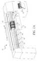
- FIG. 1Ais a perspective view that illustrates an inkjet printer including a print carriage, carriage guide members, timing belt, ink supply tubing, ink cartridges being in accordance with the invention, a recording element, and sheet transport roller;
- FIG. 1Bis a perspective view showing a single color inkjet printhead used in the multicolor printer of FIG. 1A;
- FIG. 1Cis a plan view illustrating the nozzle plate for the printhead of FIG. 1B;
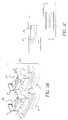
- FIG. 2is a perspective view of an ink cartridge receiver assembly used in the printer of FIG. 1;
- FIG. 3is a top plan view of the ink cartridge receiver assembly including six ink cartridges, the ink cartridges being in accordance with the invention
- FIG. 4is a different perspective view of the ink cartridge receiver assembly used in the printer of FIG. 1;
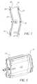
- FIG. 5is a perspective view of the ink cartridge of the invention.
- FIG. 6shows a bottom view of the ink cartridge including the alignment features, memory chip assembly, color identifier, and curvaceous shape
- FIGS. 7 and 8show ink cartridge alignment features engaging with the separators in the ink cartridge receiver assembly
- FIGS. 9A and 9Bshow how the color identifier keyway and color identifier key tab interface when the ink cartridge is placed in the receiver assembly the FIGS. showing respectively and incorrect cartridge being attempted to be placed in the receptacle and a proper ink cartridge being placed in the receptacle;
- FIG. 10shows receipt of an ink withdrawal needle from the receptacle being engaged with an ink bag that is internal to the ink cartridge
- FIG. 11is an exploded view showing the ink bag, fitment and the septum and ink withdrawal needle which needle forms part of a receptacle in the cartridge receiver assembly;
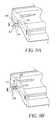
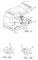
- FIG. 12is an exploded view of the ink cartridge of the invention.
- FIGS. 13A and 13Bis a perspective view illustrating details of the memory chip assembly
- FIG. 14is a perspective view of an ink cartridge housing half and a memory chip assembly being mounted in the housing half;
- FIG. 15is an exploded view illustrating the details of assembly and shows the details of the ink bag fitment, septum, color identifier, memory chip assembly, ink cartridge housing half and the ink withdrawal needle which forms part of the receptacle, the view being taken from the underside of the cartridge half;
- FIG. 16is an exploded view illustrating further details of assembly wherein the color identifier traps the fitment and forms a collar thereabout;
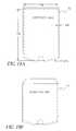
- FIG. 17is a schematic of a cross-section of the ink cartridge illustrating support by the internal surfaces of the ink cartridge of the filled ink bag;
- FIG. 18is a schematic of a front and right side view of the ink cartridge of the invention and illustrating an internal height dimension
- FIG. 19 A and FIG. 19Bare front side elevational views of the ink bag that is to be positioned in the cartridge and showing respectively the ink bag in a fully stretched condition and the ink bag when it is not stretched;
- FIG. 20is a perspective view of the ink bag.
- FIGS. 1A-Cshows an embodiment of a printer 10 that is adapted to accept a plurality of the ink cartridges of the invention as a main ink supply.
- the printerincludes a carriage 11 that supports an ink jet print head for movement during printing.
- the ink jet print headis mounted on a print head module 25 (FIG. 1B) which in turn is mounted to the carriage 11 .
- the carriage 11is coupled through a timing belt 13 with a drive motor (not shown), is reproducibly movable along the width of a recording medium 12 (in the directions of arrows A and B in the FIG. 1 A), while being guided by a guide member 15 .
- the ink jet print head 31receives ink from the ink tank or cartridge 16 through an ink supply tube 17 .
- An intermediate supply of inkmay be provided between the ink cartridge and print head, and thus the ink cartridge may be considered a bulk supply of the ink of a particular color for the printer.
- a sheet transport roller 18when driven by a drive motor (not shown), transports the recording medium 12 in the direction (of arrow C in the FIG. 1A) perpendicular to the moving direction of the carriage 11 .
- a Raster Image Processorcontrols image manipulation and the resultant image file is delivered to the printer via a remotely located computer through a communications port.
- On board memorystores the image file while the printer is in operation.
- FIGS. 1B and 1Cshow an embodiment of a piezoelectric print head module or assembly 25 .
- the ink cartridge of the inventionmay be used with other drop-on-demand print heads such as thermal inkjet print heads and continuous inkjet print heads.
- Reference numeral 36designates a nozzle plate having nozzle openings 37 formed therein.
- Numeral 38indicates an ink supply port through which ink flows from the ink cartridges 16 via the ink supply tube 17 .
- the firing rate of the print head 31can be switched between 7.5 kHz and 15 kHz depending on the selection of image resolution and print quality.
- the carriage velocityis fixed in all print modes.
- a printer main ink supply 19that includes a plurality of different color ink containing ink cartridges 16 and ink cartridge receiver assembly 20 that includes individual cartridge receiving receptacles for receiving each cartridge.
- Six ink cartridges 16are positioned in the assembly housing of the ink cartridge receiver assembly such that they are each separated by a divider wall or spacer wall 23 that forms a part of the receiver assembly.
- the ink cartridge 16is comprised of a housing 50 with a non-symmetrical curvaceous profile 51 , integrated hand hold features or handle 53 , cartridge alignment features 52 , ink cartridge color identifier or color or ink type discrimination structure 60 , and a memory chip assembly 55 .
- An ink bag 70is also supported within the cartridge and contains ink of a particular color.
- the ink color usedmay be cyan, magenta, yellow and black. Different shades of one or more of these colors may also be provided. Thus, for example, there may be provided cartridges with different shades of cyan. A spot color may also be provided, thus providing an option for use of a very particular color.
- the cartridge housingincludes an ink receiving cavity, and the housing is defined by a front side wall 90 , a back side wall 91 opposite the front side wall, a left side wall 94 and a right side wall 93 , the left side wall and the right side wall each respectively establishing a spacing between the front side wall and the back side wall.
- a bottom wall 95is also provided from which ink is removed from the ink cartridge.
- the front side wall and the back side wallare curved so that an outer surface of one has a generally convex curvature and the outer surface of the other has a concave curvature.
- a plurality of alignment recesses or features 52are formed on the surfaces of the cartridge housing.
- a first alignment recess 52is formed on the outer surface of the front side wall and a pair of alignment recesses 52 are formed on the outer surface of the back side wall.
- the three alignment recessesare formed adjacent to the bottom wall and the first alignment recess is located substantially midway between the pair of alignment recesses in the width-wise direction of the ink receiving cavity.
- the recesses 52are each relatively elongated in the direction of the height of the cartridge and this is advantageous since the cartridge is inserted with the bottom of the cartridge moving towards the bottom of the ink cartridge receiving receptacle. Therefore, the elongation of the recesses are in the direction of insertion of the cartridges into a respective receptacle.
- the walls of the ink cartridgeare relatively rigid to provide a rigid cartridge structure.
- a plurality of identical spacer walls spaced equally from each other in the assembly housingalso have cartridge alignment structures 24 thereon (see also FIGS. 6 and 7 ).
- Each spacer wall 23has a curvature to receive a cartridge having a generally complementary curvature to the curvature of the spacer wall.
- Adjacent spacer walls 23define a cartridge receiving receptacle and have facing surfaces wherein the location of alignment structures 24 are not identical since the alignment recesses on the front and back surfaces of the cartridge are not identical.
- the curvaceous profile 51 of the cartridge 16is comprised of various radii and appears in a wave shape. This shape can be other non-rectangular shapes such that when nested with other cartridges the orientation of insertion is unidirectional.
- the provision of a curved shape to the ink cartridgeprovides a visual aid in describing the proper orientation of the ink cartridge before insertion.
- the general shape of the cartridge and that of the cartridge receiving receptacle forming a part of the cartridge receiver assemblyprevents the cartridge from being inserted incorrectly. This permits electrical contacts forming a part of the memory chip assembly to be aligned with electrical contact members 21 (FIG. 4) in the receptacles of the cartridge receiver assembly 20 .
- the curvaceous profile 51also stabilizes the ink cartridge when in storage by providing nesting action as cartridges are stacked one on top of the other.
- the ink cartridge housing(FIGS. 5, 6 ) includes integral alignment features 52 that are molded into the plastic cartridge that mate or cooperate with location structures or features formed in the receptacles of the ink cartridge receiver assembly 19 (FIG. 3 ).
- the opening of each receptacleis significantly larger than the ink cartridge allowing for easy insertion.
- the ink cartridge's alignment features 52engage with mating location features 24 on the divider or spacer walls 23 (FIG. 7) as the ink cartridge 16 is being inserted into the proper receptacle of the ink cartridge receiver assembly 19 . Engagement of these features occurs before the receptacle's ink color identifier key and needle approach the cartridge fitment 71 and septum 72 (FIG. 11 ).
- the cartridge alignment features 52also align the ink cartridge such that the electrical contact members 21 (FIG. 4) of each cartridge receiving receptacle are positioned to engage the counterpart electrical contacts 58 of memory chip assembly 55 (FIGS. 13A and 13B) on the ink cartridge 16 .
- the divider walls 23 , the ink cartridge housing 50 (FIG. 5) and color identifier (color or ink type discrimination structure) 60are the same parts used repeatedly in the ink cartridge assembly 20 .
- the difference from one color cartridge to the nextis the orientation difference of the color identifier 60 in concert with the orientation difference of the color identifier key tab 67 (see FIGS. 9A and 9B) from one cartridge receiving receptacle to another cartridge receiving receptacle.
- This designtherefore minimizes the manufacturing cost of the ink cartridge assembly 20 by using a minimum number of unique components.
- FIG. 12shows an exploded view of the ink cartridge 16 along with the color identifier key assembly 66 .
- the color identifier 60is composed of two plastic molded components 61 and 62 . During assembly of the cartridge with the ink bag therein, the ink bag fitment extends from the cartridge bottom housing.
- the ink bag fitment 71is trapped within the color identifier components 61 and 62 which are mated together and which form a collar thereabout, and thereby secure the fitment for presentation to the needle 74 during ink cartridge insertion into the receiver assembly 20 .
- an octagon shaped member 80 on and molded integral with the color identifier 60mates with an octagonal recess 65 molded in the wall of the bottom surface of the ink cartridge housing 50 .
- the ink cartridge housing 50is formed of housing halves 50 a and 50 b that are ultrasonically welded together to assemble the cartridge with the various parts such as the ink color identifier 60 and memory chip assembly 55 secured thereto.
- Each housing halfincludes a recess 65 a , 65 b that defines four surfaces of the eight surfaces of the octagonal recess 65 .
- the color identifier 60can be oriented in eight unique angular positions each being specific to one of eight different ink colors prior to assembly of the cartridge housing halves. Although eight unique positions are illustrated for this particular ink cartridge this is but an example, and generally speaking the color identifier may be oriented in plural positions to provide for color or ink type discrimination for plural different ink containing cartridges. Although there is shown that an octagonal member rests within a recess formed in the cartridge housing, other positioning structures can be used for positioning purposes to allow support for a member to be changed in orientation so that the same parts can be used for different color ink cartridges.
- the color identifieris a generally cylindrical member and can be rotated about the central axis thereof prior to assembly of the cartridge housing halves and placed in the octagonal recess in a manner appropriate for the color of the ink to be placed in the cartridge.
- the color identifier 60can be broadly referred to as a color or ink type discrimination structure.
- the color identifier 60is positioned in the octagonal recess 65 of the ink cartridge housing halves 50 a , 50 b in a unique orientation for each color or ink type to be placed in the ink cartridge 16 and assembled.
- the color identifier key tab 67is located at the bottom of the ink cartridge receiver assembly and is oriented such that only one color of ink in a specific ink cartridge can be fully inserted. If the color identifier key tab 67 is aligned with the key slot or keyway 68 in the color identifier 60 as shown by configuration 63 (see FIG. 9 B), then full engagement of the needle 74 with the septum 72 will be accomplished (FIG. 10 ).
- the orientation of the color identifier key tab 67will not line up with the keyway 68 in the color identifier 60 as shown by configuration 64 (FIG. 9 A). Engagement of the needle 74 with the septum 72 will be prevented and therefore cross contamination of two different colors of ink will be avoided.
- These color identifier featuresdo not align the cartridge to the cartridge receiving receptacle but only prevent full insertion of the ink cartridge in the cartridge receiving receptacle if the cartridge is filled with a color of ink not intended for that receptacle.
- This color identification methodallows for the same parts to be used for every color cartridge with only a unique orientation change made during the cartridge assembly process. Therefore, the number of manufacturing tools and number of unique parts required in inventory to produce cartridges adapted to contain ink of various colors is minimized and costs to produce them reduced.
- a sealmay be provided over the septum and color identifier 60 after assembly of the cartridge parts.
- a non-volatile memory chip assembly 55constructed using a rigid circuit board 57 , non-volatile memory chip 59 and gold contacts 58 , is located within a pocket 56 integrally molded on the ink cartridge housing.
- the pocket 56includes integral locating features for receiving the memory to assembly.
- the pocket including these integral featuresare molded as part of the ink cartridge housing and retain the memory chip assembly 55 once the housing is assembled.
- Each cartridge housing halfincludes structure for defining the pocket 56 .
- the location of the memory chip assembly relative to the ink cartridge housingis controlled strictly by the integral features and therefore does not require any manual or automated alignment fixturing for assembly purposes.
- each cartridge housing halfincludes a slot formed in the bottom wall of the cartridge and/or on the inside wall of the cartridge to define the pocket structure 56 about an aperture 82 formed in the bottom wall of the cartridge.
- the apertureactually has aperture parts 82 a and 82 b formed in respective housing halves 50 a and 50 b .
- the housing halves of the cartridgecannot come together during assembly of the cartridge unless the chamfer 75 on the circuit board is properly located in the pocket structure and particularly in the pocket portion having the mating filled in area 76 which is generally complementary in shape to the chamfer 75 . This insures proper orientation of the memory chip assembly during the assembly process.
- the location tolerance of the gold contacts relative to the electrical contacts on the ink cartridge receiver assembly, once retained by the housing,is dependent on the capability of the injection molding process.
- the size of the gold electrically conductive electrical contacts 58has been increased to a point allowing for economical tolerances to be applied to all the associated components relating to the alignment of the memory chip gold contacts to the electrical contacts.
- the area of each of the two circular electrical contacts 58is equivalent to a circle having a diameter of about 1 ⁇ 4 of an inch (6.3 millimeters). While a circular area is shown for each electrical contact 58 , other relatively large electrically conductive areas of different configuration may be used.
- the memory chip 59may be of the type sold by Dallas Semiconductor Corp. of Dallas, Tex., U.S.A. such as, for example, chip DS 2502, and feature one line served by one electrical contact of the circuit board 57 for providing data to and from the printer's computer controller.
- the second line and served by the second electrical contact of the circuit board 57may be for a ground reference connection.
- Traces leading from the memory chipconnect with throughways or vias 54 that pass through the circuit board and connect with the electrical contacts 58 formed on the other side of the circuit board.
- the ends of the circuit boardsmay have “mouse bites” which are common in the manufacture of small circuit boards.
- the memory chip assembly 55that is received within a pocket structure 56 formed in the cartridge bottom that includes integral mating features as part of the ink cartridge housing 50 .
- the memory chip assembly 55consists of a circuit board 57 , a memory chip 59 , and electrical contacts 58 (FIGS. 13 A and 13 B).
- the circuit boardis rigid and inserted into the pocket structure 56 .
- the integral features of the pocket structureare molded as part of the ink cartridge housing and retain the memory chip assembly once the housing is assembled with the electrical contacts 58 facing outwardly through an aperture 82 formed in the bottom side of the cartridge.
- a chamfer 75 or other suitable structure for restricting insertion of the circuit board into the pocket in only one-wayis added to one corner of the rigid circuit board.
- a cooperating structure provided in the pocket structuresuch as the filled in area 76 (FIG. 14) is formed as part of the integral locating feature of the pocket structure on the cartridge housing. This insures proper orientation of the memory chip assembly and particularly the respective electrical contacts thereof during the assembly process.
- the location tolerance of the gold contacts relative to the electrical contacts on the ink cartridge receiver assembly, once retained by the housing,is dependent on the capability of the injection molding process.
- Other contributing tolerancesinclude the size of the rigid circuit board, the location tolerance of the gold contacts on the rigid circuit board 57 , and the location tolerances of the components within the ink cartridge receiver assembly 19 including the location tolerance associated with the electrical contacts 54 .
- the size of the gold contacts 58are substantially increased to a point (a circular area of each is about 1 ⁇ 4 of an inch in diameter) allowing for economical tolerances to be applied to all the associated components relating to the alignment of the memory chip gold contacts to the electrical contacts.
- the fitment 71is thermally sealed to the bag material.
- the flexible ink bag materialis composed of three layers with adhesive between each layer. Each layer has a specific purpose by providing either compatibility with the ink, low water vapor and gas permeability, or abrasion resistance.
- the inside layer, in contact with the ink,is either a linear low density or low density polyethylene.
- the fitmentis made front a high-density polyethylene thereby promoting good adhesion of it to the bag during the thermal welding process.
- the middle layeris aluminum foil providing low water vapor and gas permeability
- the outer layeris either nylon or polyethylene terepthalate having high strength and abrasion resistance.
- the septum 72is inserted into the circular opening of the fitment 71 .
- the inside diameter of the circular opening of the fitmentis smaller than the outside diameter of the septum creating a slight compression of the septum once inserted into the fitment.
- the bag, fitment and septummust allow for an efficient filling and evacuation process.
- a feature to the function of the ink bagis the taper angle 73 illustrated in FIG. 11 .
- the bagis evacuated of air before ink is injected into it.
- the remaining airnow near the fitment and septum, is evacuated. If the taper angle is not present the air tends to become trapped in the corners of the bag and can not be evacuated. The angle allows the remaining air to move to the fitment and thereby allows for its removal.
- the taper angle 73which is formed from the area of the bag near the fitment and tapers to a vertical side edge of the bag should be between 5 and 45 degrees. In the preferred embodiment, a taper angle of 15 degrees is provided.
- the ink cartridge housing 50includes a volume V H within it comprising an volume to contain the ink bag 70 .
- An additional volumeis included within the cartridge housing located above V H that provides space for an integral handle 53 having a top wall 53 a .
- the cartridge handleeases transportation by the customer.
- the volume V H of the cartridge housing containing the ink bagis defined having a height H H (see FIG. 18 ), a width W H (see FIG. 17 ), and a thickness T H (see FIG. 17 ).
- the aspect ratio of the thickness T H to width W H , the cartridge height H H and the flexible ink bagdetermine the optimum relationship between the volume of ink in the bag, the remaining ink after use, and residual air remaining in the bag after filling. This relationship is defined as follows:
- T HThickness of the cartridge housing defined as the distance between the inside surfaces of the front and back side surfaces of the housing assembly.
- W HWidth of the cartridge housing defined as the distance between the inside surfaces of the left and right side surfaces of the housing assembly.
- H HHeight of the cartridge as defined as the distance from the inside surface of the bottom side of the cartridge housing to the top of the cavity designed to contain the ink bag. This does not include the additional height of the cartridge required to form the integral handle. This inside surface is molded with a draft so the measurement is taken from an edge where the cartridge housing halves are joined.
- V HInterior volume of the housing assembly containing the ink bag.
- W BOverall width of the ink bag when empty, lying flat and stretched to its full extents regardless of the presence of a gusset.
- H BOverall height of the ink bag when empty, lying flat and stretched to its full extent regardless of the presence of a gusset.
- SWSeal width of the bag, representing a seal width running along the sides of the ink bag and thus provides for a smaller inside volume of the bag.
- H BH H +T H
- the method utilized in the assembly of the ink cartridgeis benefited by the design.
- the advantage of sizing the ink bag and cartridge housing according to the relationships stated aboveallows for the assembly of the ink bag to the cartridge housing before the ink filling process is initiated.
- the process of assemblyincludes evacuating the ink bag of air, laying the first half of the cartridge housing on its side, placing color identification components around the fitment of the ink bag, and inserting the ink bag into the first housing using two sided tape.
- the insertion of the bagis made such that the empty ink bag is conformed to the profile of the first housing half, taped in place using double-sided tape, and then covered with the second housing half.
- the first and second housings halvesare then ultrasonically welded together.
- the ultrasonic welding processproviding a low cost assembly method although other known methods may be used.
- the ink bagis filled with a known amount of ink (for example, 1100 mL) while lying on its side and by placing a needle through the septum and pumping ink through the needle and into the ink bag.
- the cartridge assemblyis then turned vertically such that the fitment and septum are facing up.
- the cartridgemay be bumped to cause air in the ink to rise to the top of the bag.
- the remaining air and about 50 mL of inkare then removed from the bag by applying a vacuum through the needle.
- the ink bagis fully constrained by the housing and the surface of bag is in intimate contact with the four inside surfaces of the housing assembly as illustrated in the horizontal sectional view shown in FIG. 17 . This prevents the bag from shifting during transport.
- the front and backsidesare curved complementary; for example one is generally concave in curvature and the other is generally convex in curvature, but internally they maintain a generally uniform spacing between corresponding points on the internal surfaces at least along a certain section through the cartridge.
- the memory chipis located at the bottom side of the ink cartridge housing to allow for a simple, low cost electrical contact design for engaging the electrical contact members in the ink cartridge receiver assembly. While other places on the ink cartridge housing could be used to support the memory chip assembly 55 it is desirable that the memory chip assembly be positioned so as to avoid close proximity to the ink bag 70 .
- taper of the bag's lower edgeallows for the bag, when filled with ink, to avoid contact with the pocket structure 56 supporting the memory chip assembly. If contact is allowed, then abrasion may result and cause ink to leak from the bag.
- the bag 70 when fullcan rise over the pocket structure within the ink cartridge housing through use of the taper formed on the bag. It is preferred to position the pocket structure 56 relative to the left and right side walls of the cartridge so that the pocket structure is spaced sufficiently therefrom such that cartridge housing wall thickness remains closer to nominal wall thickness and the reliability of the mold tooling for molding these cartridges is better maintained.
- a further advantageis provided in having the mounting location of the memory chip assembly be beneath the finger hole of the handle. This relationship exists due to the way the ink cartridge receiver assembly 20 tips out for easy access to the ink cartridges. In this regard reference is made to FIGS. 1 a , 2 and 4 . Normally the ink cartridge receiver assembly 20 is positioned in the closed position (not shown) when no access to the ink cartridges is required.
- the ink cartridge receiver assemblyWhen the ink cartridge receiver assembly is tipped or pivoted outwardly as shown to provide operator access to the ink cartridges 16 , the memory chip assembly on each cartridge and the electrical contacts 21 in each cartridge receiving receptacle are tipped upwardly. This allows gravity to force any ink that has leaked from an ink cartridge to move away from the memory chip assembly and the electrical contacts as the ink cartridge receiver assembly is pivoted to the open position.
- the structure for supporting the memory chip assemblyis on the bottom wall and desirably about 8 to 9 millimeters from the inside surface of the right side wall 93 .
- the right side wallbeing the wall of the cartridge housing that would be pivoted upwardly as the cartridge receiver assembly is pivoted to the open position.
- the width dimension of the cartridge housingi.e. distance between right side wall and left side wall, limits the distance the memory chip assembly can be located away from the septum. In order to avoid contamination with ink that has leaked, it is preferred that this distance be as great as possible and because of constraints regarding placement close to the side wall an optimum location for a spacing is as noted above about 19 millimeters from the outside surface of the right side wall for the cartridge described.
- the optimum spacing of the centers of the electrical contacts 58 to the center of the septum 72is about 57 millimeters.
Landscapes
- Engineering & Computer Science (AREA)
- Manufacturing & Machinery (AREA)
- Ink Jet (AREA)
Abstract
Description
Claims (24)
Priority Applications (5)
| Application Number | Priority Date | Filing Date | Title |
|---|---|---|---|
| US09/931,521US6505926B1 (en) | 2001-08-16 | 2001-08-16 | Ink cartridge with memory chip and method of assembling |
| EP02078221AEP1285766B1 (en) | 2001-08-16 | 2002-08-05 | Ink cartridge with memory chip and method of assembling |
| DE60200265TDE60200265T2 (en) | 2001-08-16 | 2002-08-05 | Ink cartridge with memory chip and procedure for its assembly |
| JP2002236385AJP2003072103A (en) | 2001-08-16 | 2002-08-14 | Ink cartridge with memory chip and method of assembling |
| US10/263,170US6851799B2 (en) | 2001-08-16 | 2002-10-02 | Ink cartridge with memory chip and method of assembling |
Applications Claiming Priority (1)
| Application Number | Priority Date | Filing Date | Title |
|---|---|---|---|
| US09/931,521US6505926B1 (en) | 2001-08-16 | 2001-08-16 | Ink cartridge with memory chip and method of assembling |
Related Child Applications (1)
| Application Number | Title | Priority Date | Filing Date |
|---|---|---|---|
| US10/263,170ContinuationUS6851799B2 (en) | 2001-08-16 | 2002-10-02 | Ink cartridge with memory chip and method of assembling |
Publications (1)
| Publication Number | Publication Date |
|---|---|
| US6505926B1true US6505926B1 (en) | 2003-01-14 |
Family
ID=25460908
Family Applications (2)
| Application Number | Title | Priority Date | Filing Date |
|---|---|---|---|
| US09/931,521Expired - Fee RelatedUS6505926B1 (en) | 2001-08-16 | 2001-08-16 | Ink cartridge with memory chip and method of assembling |
| US10/263,170Expired - Fee RelatedUS6851799B2 (en) | 2001-08-16 | 2002-10-02 | Ink cartridge with memory chip and method of assembling |
Family Applications After (1)
| Application Number | Title | Priority Date | Filing Date |
|---|---|---|---|
| US10/263,170Expired - Fee RelatedUS6851799B2 (en) | 2001-08-16 | 2002-10-02 | Ink cartridge with memory chip and method of assembling |
Country Status (4)
| Country | Link |
|---|---|
| US (2) | US6505926B1 (en) |
| EP (1) | EP1285766B1 (en) |
| JP (1) | JP2003072103A (en) |
| DE (1) | DE60200265T2 (en) |
Cited By (26)
| Publication number | Priority date | Publication date | Assignee | Title |
|---|---|---|---|---|
| US6712459B2 (en)* | 2002-07-18 | 2004-03-30 | Eastman Kodak Company | Ink cartridge having shielded pocket for memory chip |
| US20040183871A1 (en)* | 2002-01-30 | 2004-09-23 | Childers Winthrop D. | Method and device for filling a printing-fluid container |
| US6796635B2 (en) | 2000-10-11 | 2004-09-28 | Seiko Epson Corporation | Ink cartridge and inkjet printer |
| US20050146581A1 (en)* | 2001-04-03 | 2005-07-07 | Hisashi Miyazawa | Ink cartridge |
| US20050151810A1 (en)* | 2004-01-08 | 2005-07-14 | Eastman Kodak Company | Ink container installation and alignment feature |
| US20050200670A1 (en)* | 2002-11-26 | 2005-09-15 | Kazuhiro Hashii | Ink cartridge and recording apparatus |
| US20060038863A1 (en)* | 2004-08-18 | 2006-02-23 | Eastman Kodak Company | Refillable chemical cartridge for photoprocessing equipment |
| US20060114487A1 (en)* | 2004-11-30 | 2006-06-01 | Caveney Jack E Jr | Market-based labeling system and method |
| US20060146100A1 (en)* | 2005-01-04 | 2006-07-06 | Dull Daniel J | Ink jet supply component including a secure memory serial device |
| US20070070156A1 (en)* | 2002-01-30 | 2007-03-29 | Charlie Steinmetz | Printing-fluid container |
| US20070081842A1 (en)* | 2005-10-06 | 2007-04-12 | Zih Corporation | Memory system and method for consumables of a printer |
| US7488059B1 (en)* | 2004-11-02 | 2009-02-10 | Nu-Kote International, Inc. | Enclosure for ink reservoir bag |
| US20090066768A1 (en)* | 2002-11-26 | 2009-03-12 | Seiko Epson Corporation | Ink cartridge and recording apparatus |
| US20090091779A1 (en)* | 2005-06-01 | 2009-04-09 | Canon Finetech, Inc. | Print module, information processing device, print system, print unit, ink supply unit, print method, and program |
| US20110134197A1 (en)* | 2003-08-08 | 2011-06-09 | Taku Ishizawa | Liquid container |
| CN102173208A (en)* | 2011-01-28 | 2011-09-07 | 珠海艾派克微电子有限公司 | Device and method for resetting memory chip of imaging device |
| US20120105556A1 (en)* | 2010-11-01 | 2012-05-03 | Seiko Epson Corporation | Ink cartridge assembly, cartridge assembly kit, and printer |
| US20130169718A1 (en)* | 2004-03-24 | 2013-07-04 | Seiko Epson Corporation | Attachment and attachment system |
| US20130225748A1 (en)* | 2012-02-29 | 2013-08-29 | Vladimir Jakubek | White ink compositions |
| US20140111583A1 (en)* | 2010-12-23 | 2014-04-24 | Marabu Gmbh & Co. Kg | Ink cartridge for inkjet printers |
| US9233504B2 (en) | 2012-10-29 | 2016-01-12 | Makerbot Industries, Llc | Tagged build material for three-dimensional printing |
| US9296214B2 (en) | 2004-07-02 | 2016-03-29 | Zih Corp. | Thermal print head usage monitor and method for using the monitor |
| US9907633B2 (en)* | 2012-09-28 | 2018-03-06 | Stephen H. Wolpo | Oral care system with mouthpiece |
| WO2020046326A1 (en)* | 2018-08-30 | 2020-03-05 | Hewlett-Packard Development Company, L.P. | Electrical contacts coupled to guide structures |
| US11312138B2 (en)* | 2016-02-02 | 2022-04-26 | Seiko Epson Corporation | Liquid ejecting unit, liquid ejecting head, support body for liquid ejecting head |
| US11865845B2 (en) | 2018-08-30 | 2024-01-09 | Hewlett-Packard Development Company, L.P. | Print material refill device |
Families Citing this family (30)
| Publication number | Priority date | Publication date | Assignee | Title |
|---|---|---|---|---|
| US7431436B1 (en)* | 2002-11-12 | 2008-10-07 | Vutek, Incorporated | Identification system for inks in printing systems |
| JP2004284093A (en)* | 2003-03-20 | 2004-10-14 | Ricoh Co Ltd | Ink bag retaining member, ink cartridge, and inkjet recording device |
| JP2004284094A (en)* | 2003-03-20 | 2004-10-14 | Ricoh Co Ltd | Ink cartridge and ink jet recording apparatus |
| JP4529405B2 (en)* | 2003-09-30 | 2010-08-25 | ブラザー工業株式会社 | Inkjet recording device |
| US7448734B2 (en)* | 2004-01-21 | 2008-11-11 | Silverbrook Research Pty Ltd | Inkjet printer cartridge with pagewidth printhead |
| US7731327B2 (en)* | 2004-01-21 | 2010-06-08 | Silverbrook Research Pty Ltd | Desktop printer with cartridge incorporating printhead integrated circuit |
| US7425050B2 (en)* | 2004-01-21 | 2008-09-16 | Silverbrook Research Pty Ltd | Method for facilitating maintenance of an inkjet printer having a pagewidth printhead |
| US7547092B2 (en)* | 2004-01-21 | 2009-06-16 | Silverbrook Research Pty Ltd | Method for facilitating the upgrade of an inkjet printer |
| US7441865B2 (en) | 2004-01-21 | 2008-10-28 | Silverbrook Research Pty Ltd | Printhead chip having longitudinal ink supply channels |
| US7232208B2 (en)* | 2004-01-21 | 2007-06-19 | Silverbrook Research Pty Ltd | Inkjet printer cartridge refill dispenser with plunge action |
| US7121655B2 (en)* | 2004-01-21 | 2006-10-17 | Silverbrook Research Pty Ltd | Inkjet printer cartridge refill dispenser |
| US7097291B2 (en)* | 2004-01-21 | 2006-08-29 | Silverbrook Research Pty Ltd | Inkjet printer cartridge with ink refill port having multiple ink couplings |
| US7303255B2 (en)* | 2004-01-21 | 2007-12-04 | Silverbrook Research Pty Ltd | Inkjet printer cartridge with a compressed air port |
| US7175266B2 (en)* | 2004-01-30 | 2007-02-13 | Hewlett-Packard Development Company, L.P. | Replaceable memory device for a consumable substance container, and methods |
| JPWO2006019034A1 (en)* | 2004-08-20 | 2008-05-08 | コニカミノルタエムジー株式会社 | Ink cartridge for ink jet recording apparatus |
| US7976138B2 (en)* | 2006-12-21 | 2011-07-12 | Eastman Kodak Company | Data-providing-component securing mechanism for printing apparatus reservoir |
| US7731335B2 (en)* | 2006-12-21 | 2010-06-08 | Eastman Kodak Company | Data storage device mounting arrangement for printing device |
| US8061826B2 (en)* | 2008-07-31 | 2011-11-22 | Static Control Components, Inc. | Methods and devices for remanufacturing an imaging cartridge |
| US8356874B2 (en) | 2009-04-08 | 2013-01-22 | Redwood Technologies, Llc | Apparatus and method for precision application and metering of a two-part (binary) imaging solution in an ink jet printer |
| US8960880B2 (en) | 2009-04-08 | 2015-02-24 | Redwood Technologies, Llc | Binary epoxy ink and enhanced printer systems, structures, and associated methods |
| JP4728421B2 (en)* | 2009-11-16 | 2011-07-20 | エスアイアイ・プリンテック株式会社 | Pressure buffer and droplet jet recording apparatus |
| US8544995B2 (en)* | 2010-12-28 | 2013-10-01 | Brother Kogyo Kabushiki Kaisha | Ink cartridge |
| EP2798497A2 (en)* | 2011-12-30 | 2014-11-05 | ZIH Corp. | Enhanced printer functionality and maintenance with dynamic identifier code |
| EP2817708B1 (en) | 2012-02-21 | 2020-08-26 | Zebra Technologies Corporation | Method and apparatus for implementing near field communications with a printer |
| US8823990B2 (en) | 2012-12-31 | 2014-09-02 | International Business Machines Corporation | Print job distribution within a printing system |
| JP6163890B2 (en)* | 2013-06-06 | 2017-07-19 | セイコーエプソン株式会社 | Liquid supply device, liquid container |
| JP6303349B2 (en)* | 2013-09-17 | 2018-04-04 | 株式会社リコー | Liquid cartridge and image forming apparatus |
| JP6402457B2 (en)* | 2014-03-14 | 2018-10-10 | セイコーエプソン株式会社 | Liquid container |
| JP6337719B2 (en)* | 2014-09-24 | 2018-06-06 | ブラザー工業株式会社 | Printing device |
| CN111051066B (en) | 2017-10-05 | 2021-12-10 | 惠普发展公司,有限责任合伙企业 | Supply container with alignment member |
Citations (24)
| Publication number | Priority date | Publication date | Assignee | Title |
|---|---|---|---|---|
| DE3405164A1 (en) | 1984-02-14 | 1985-08-22 | Olympia Werke Ag, 2940 Wilhelmshaven | Ink supply container for ink jet printers |
| US4961088A (en) | 1989-04-20 | 1990-10-02 | Xerox Corporation | Monitor/warranty system for electrostatographic reproducing machines using replaceable cartridges |
| USD341157S (en) | 1990-12-10 | 1993-11-09 | Seiko Epson Corporation | Ink bag for printer |
| US5266968A (en) | 1992-03-27 | 1993-11-30 | Eastman Kodak Company | Non-volatile memory thermal printer cartridge |
| US5410641A (en) | 1991-10-23 | 1995-04-25 | Seiko Epson Corporation | Intelligent cartridge for attachment to a printer to perform image processing tasks in a combination image processing system and method of image processing |
| US5506611A (en) | 1989-08-05 | 1996-04-09 | Canon Kabushiki Kaisha | Replaceable ink cartridge having surface wiring resistance pattern |
| US5610635A (en) | 1994-08-09 | 1997-03-11 | Encad, Inc. | Printer ink cartridge with memory storage capacity |
| US5666146A (en) | 1991-05-27 | 1997-09-09 | Seiko Epson Corporation | Ink cartridge for ink jet recording apparatus |
| US5788388A (en) | 1997-01-21 | 1998-08-04 | Hewlett-Packard Company | Ink jet cartridge with ink level detection |
| US5835817A (en) | 1994-12-22 | 1998-11-10 | Hewlett Packard Company | Replaceable part with integral memory for usage, calibration and other data |
| US5860363A (en) | 1997-01-21 | 1999-01-19 | Hewlett-Packard Company | Ink jet cartridge with separately replaceable ink reservoir |
| US5956057A (en) | 1996-08-30 | 1999-09-21 | Hewlett-Packard Company | Ink container having electronic and mechanical features enabling plug compatibility between multiple supply sizes |
| US6000773A (en) | 1994-08-09 | 1999-12-14 | Encad, Inc. | Ink jet printer having ink use information stored in a memory mounted on a replaceable printer ink cartridge |
| US6019449A (en) | 1998-06-05 | 2000-02-01 | Hewlett-Packard Company | Apparatus controlled by data from consumable parts with incorporated memory devices |
| US6130695A (en)* | 1995-04-27 | 2000-10-10 | Hewlett-Packard Company | Ink delivery system adapter |
| US6151039A (en) | 1997-06-04 | 2000-11-21 | Hewlett-Packard Company | Ink level estimation using drop count and ink level sense |
| US6164743A (en) | 1996-04-17 | 2000-12-26 | Hewlett-Packard Company | Ink container with an inductive ink level sense |
| US6168262B1 (en) | 1997-01-30 | 2001-01-02 | Hewlett-Packard Company | Electrical interconnect for replaceable ink containers |
| US6183077B1 (en)* | 1995-04-27 | 2001-02-06 | Hewlett-Packard Company | Method and apparatus for keying ink supply containers |
| US6203147B1 (en) | 1994-12-22 | 2001-03-20 | Hewlett-Packard Company | Electrical and fluidic interface for an ink supply |
| US6227638B1 (en) | 1997-01-21 | 2001-05-08 | Hewlett-Packard Company | Electrical refurbishment for ink delivery system |
| US6227643B1 (en) | 1997-05-20 | 2001-05-08 | Encad, Inc. | Intelligent printer components and printing system |
| US6416166B1 (en)* | 2001-08-16 | 2002-07-09 | Eastman Kodak Company | Ink cartridge with alignment features and method of inserting cartridge into a printer receptacle |
| USD462089S1 (en)* | 2001-08-16 | 2002-08-27 | Eastman Kodak Company | Ink cartridge |
Family Cites Families (5)
| Publication number | Priority date | Publication date | Assignee | Title |
|---|---|---|---|---|
| US5710579A (en)* | 1995-05-04 | 1998-01-20 | Calcomp Inc. | Sensor system for printers |
| JPH11297906A (en)* | 1998-03-23 | 1999-10-29 | Motorola Inc | Electronic assembly and its manufacture |
| EP2179848A1 (en)* | 1998-05-18 | 2010-04-28 | Seiko Epson Corporation | Ink-jet printing apparatus and ink cartridge therefor |
| JP2001187457A (en)* | 1998-11-26 | 2001-07-10 | Seiko Epson Corp | Printing devices and cartridges |
| GB2354202B (en)* | 2000-08-07 | 2002-09-18 | Dynamic Cassette Int | A printer cartridge kit and method |
- 2001
- 2001-08-16USUS09/931,521patent/US6505926B1/ennot_activeExpired - Fee Related
- 2002
- 2002-08-05EPEP02078221Apatent/EP1285766B1/ennot_activeExpired - Lifetime
- 2002-08-05DEDE60200265Tpatent/DE60200265T2/ennot_activeWithdrawn - After Issue
- 2002-08-14JPJP2002236385Apatent/JP2003072103A/enactivePending
- 2002-10-02USUS10/263,170patent/US6851799B2/ennot_activeExpired - Fee Related
Patent Citations (24)
| Publication number | Priority date | Publication date | Assignee | Title |
|---|---|---|---|---|
| DE3405164A1 (en) | 1984-02-14 | 1985-08-22 | Olympia Werke Ag, 2940 Wilhelmshaven | Ink supply container for ink jet printers |
| US4961088A (en) | 1989-04-20 | 1990-10-02 | Xerox Corporation | Monitor/warranty system for electrostatographic reproducing machines using replaceable cartridges |
| US5506611A (en) | 1989-08-05 | 1996-04-09 | Canon Kabushiki Kaisha | Replaceable ink cartridge having surface wiring resistance pattern |
| USD341157S (en) | 1990-12-10 | 1993-11-09 | Seiko Epson Corporation | Ink bag for printer |
| US5666146A (en) | 1991-05-27 | 1997-09-09 | Seiko Epson Corporation | Ink cartridge for ink jet recording apparatus |
| US5410641A (en) | 1991-10-23 | 1995-04-25 | Seiko Epson Corporation | Intelligent cartridge for attachment to a printer to perform image processing tasks in a combination image processing system and method of image processing |
| US5266968A (en) | 1992-03-27 | 1993-11-30 | Eastman Kodak Company | Non-volatile memory thermal printer cartridge |
| US6000773A (en) | 1994-08-09 | 1999-12-14 | Encad, Inc. | Ink jet printer having ink use information stored in a memory mounted on a replaceable printer ink cartridge |
| US5610635A (en) | 1994-08-09 | 1997-03-11 | Encad, Inc. | Printer ink cartridge with memory storage capacity |
| US5835817A (en) | 1994-12-22 | 1998-11-10 | Hewlett Packard Company | Replaceable part with integral memory for usage, calibration and other data |
| US6203147B1 (en) | 1994-12-22 | 2001-03-20 | Hewlett-Packard Company | Electrical and fluidic interface for an ink supply |
| US6130695A (en)* | 1995-04-27 | 2000-10-10 | Hewlett-Packard Company | Ink delivery system adapter |
| US6183077B1 (en)* | 1995-04-27 | 2001-02-06 | Hewlett-Packard Company | Method and apparatus for keying ink supply containers |
| US6164743A (en) | 1996-04-17 | 2000-12-26 | Hewlett-Packard Company | Ink container with an inductive ink level sense |
| US5956057A (en) | 1996-08-30 | 1999-09-21 | Hewlett-Packard Company | Ink container having electronic and mechanical features enabling plug compatibility between multiple supply sizes |
| US5788388A (en) | 1997-01-21 | 1998-08-04 | Hewlett-Packard Company | Ink jet cartridge with ink level detection |
| US5860363A (en) | 1997-01-21 | 1999-01-19 | Hewlett-Packard Company | Ink jet cartridge with separately replaceable ink reservoir |
| US6227638B1 (en) | 1997-01-21 | 2001-05-08 | Hewlett-Packard Company | Electrical refurbishment for ink delivery system |
| US6168262B1 (en) | 1997-01-30 | 2001-01-02 | Hewlett-Packard Company | Electrical interconnect for replaceable ink containers |
| US6227643B1 (en) | 1997-05-20 | 2001-05-08 | Encad, Inc. | Intelligent printer components and printing system |
| US6151039A (en) | 1997-06-04 | 2000-11-21 | Hewlett-Packard Company | Ink level estimation using drop count and ink level sense |
| US6019449A (en) | 1998-06-05 | 2000-02-01 | Hewlett-Packard Company | Apparatus controlled by data from consumable parts with incorporated memory devices |
| US6416166B1 (en)* | 2001-08-16 | 2002-07-09 | Eastman Kodak Company | Ink cartridge with alignment features and method of inserting cartridge into a printer receptacle |
| USD462089S1 (en)* | 2001-08-16 | 2002-08-27 | Eastman Kodak Company | Ink cartridge |
Non-Patent Citations (6)
| Title |
|---|
| USSN 09/931,313 filed Aug. 16, 2001, Ink Cartridge with Internal Ink Bag and Method of Filling, R. Winfield Trafton, et al. |
| USSN 09/931,420 filed Aug. 16, 2001, Ink Cartridge with Alignment Features and Method of Inserting Cartridge into a Printer Receptacle, Scott C. Robinson et al. |
| USSN 09/931,523 filed Aug. 16, 2001, Ink Cartridge with Color Discrimination Structure, R. Winfield Trafton, et al. |
| USSN 29/146,819 filed Aug. 16, 2001, Ink Cartridge with Ink Color Discrimination Structure, R. Winfield Trafton, et al. |
| USSN 29/146,820 filed Aug. 16, 2001, Ink Cartridge, R. Winfield Trafton et al. |
| USSN 29/146,821 filed Aug. 16, 2001, Ink Cartridge with Integral Handle, R. Winfield Trafton, et al. |
Cited By (62)
| Publication number | Priority date | Publication date | Assignee | Title |
|---|---|---|---|---|
| US7040744B2 (en) | 2000-10-11 | 2006-05-09 | Seiko Epson Corporation | Ink cartridge and inkjet printer |
| US6796635B2 (en) | 2000-10-11 | 2004-09-28 | Seiko Epson Corporation | Ink cartridge and inkjet printer |
| US20050030340A1 (en)* | 2000-10-11 | 2005-02-10 | Seiko Epson Corporation | Ink cartridge and inkjet printer |
| US7237882B2 (en) | 2001-04-03 | 2007-07-03 | Seiko Epson Corporation | Ink cartridge having retaining structure and recording apparatus for receiving the ink cartridge |
| US20050146581A1 (en)* | 2001-04-03 | 2005-07-07 | Hisashi Miyazawa | Ink cartridge |
| US7325915B2 (en) | 2001-04-03 | 2008-02-05 | Seiko Epson Corporation | Ink cartridge having retaining structure |
| US20050174404A1 (en)* | 2001-04-03 | 2005-08-11 | Hisashi Miyazawa | Ink cartridge |
| US7452061B2 (en)* | 2002-01-30 | 2008-11-18 | Hewlett-Packard Development Company, L.P. | Method and device for filling a printing-fluid container |
| US20070070156A1 (en)* | 2002-01-30 | 2007-03-29 | Charlie Steinmetz | Printing-fluid container |
| US20040183871A1 (en)* | 2002-01-30 | 2004-09-23 | Childers Winthrop D. | Method and device for filling a printing-fluid container |
| US7959271B2 (en)* | 2002-01-30 | 2011-06-14 | Hewlett-Packard Development Company, L.P. | Printing-fluid container |
| US6712459B2 (en)* | 2002-07-18 | 2004-03-30 | Eastman Kodak Company | Ink cartridge having shielded pocket for memory chip |
| US7669993B2 (en) | 2002-11-26 | 2010-03-02 | Seiko Epson Corporation | Ink cartridge and recording apparatus |
| US20090066768A1 (en)* | 2002-11-26 | 2009-03-12 | Seiko Epson Corporation | Ink cartridge and recording apparatus |
| US20060152564A1 (en)* | 2002-11-26 | 2006-07-13 | Kazuhiro Hashii | Ink cartridge and recording apparatus |
| US7686441B2 (en) | 2002-11-26 | 2010-03-30 | Seiko Epson Corporation | Ink cartridge and recording apparatus |
| US20070103522A1 (en)* | 2002-11-26 | 2007-05-10 | Kazuhiro Hashii | Ink cartridge and recording apparatus |
| US20070103515A1 (en)* | 2002-11-26 | 2007-05-10 | Kazuhiro Hashii | Ink cartridge and recording apparatus |
| US7237883B2 (en) | 2002-11-26 | 2007-07-03 | Seiko Epson Corporation | Ink cartridge having positioning structure and recording apparatus for receiving the ink cartridge |
| US20050200670A1 (en)* | 2002-11-26 | 2005-09-15 | Kazuhiro Hashii | Ink cartridge and recording apparatus |
| US7244018B2 (en) | 2002-11-26 | 2007-07-17 | Seiko Epson Corporation | Ink cartridge having retaining structure and memory |
| US20110134197A1 (en)* | 2003-08-08 | 2011-06-09 | Taku Ishizawa | Liquid container |
| US20120249698A1 (en)* | 2003-08-08 | 2012-10-04 | Taku Ishizawa | Liquid container |
| US8210670B2 (en)* | 2003-08-08 | 2012-07-03 | Seiko Epson Corporation | Liquid container |
| US8668317B2 (en)* | 2003-08-08 | 2014-03-11 | Seiko Epson Corporation | Liquid container |
| US20050151810A1 (en)* | 2004-01-08 | 2005-07-14 | Eastman Kodak Company | Ink container installation and alignment feature |
| US7165833B2 (en) | 2004-01-08 | 2007-01-23 | Eastman Kodak Company | Ink container installation and alignment feature |
| US9669635B2 (en) | 2004-03-24 | 2017-06-06 | Seiko Epson Corporation | Attachment and attachment system |
| US20130169718A1 (en)* | 2004-03-24 | 2013-07-04 | Seiko Epson Corporation | Attachment and attachment system |
| US8974043B2 (en)* | 2004-03-24 | 2015-03-10 | Seiko Epson Corporation | Attachment and attachment system |
| US10315438B2 (en) | 2004-07-02 | 2019-06-11 | Zebra Technologies Corporation | Thermal print head usage monitor and method for using the monitor |
| US9296214B2 (en) | 2004-07-02 | 2016-03-29 | Zih Corp. | Thermal print head usage monitor and method for using the monitor |
| US20060038863A1 (en)* | 2004-08-18 | 2006-02-23 | Eastman Kodak Company | Refillable chemical cartridge for photoprocessing equipment |
| US7488059B1 (en)* | 2004-11-02 | 2009-02-10 | Nu-Kote International, Inc. | Enclosure for ink reservoir bag |
| US20060114487A1 (en)* | 2004-11-30 | 2006-06-01 | Caveney Jack E Jr | Market-based labeling system and method |
| US9116641B2 (en) | 2004-11-30 | 2015-08-25 | Panduit Corp. | Market-based labeling system and method |
| US20060146100A1 (en)* | 2005-01-04 | 2006-07-06 | Dull Daniel J | Ink jet supply component including a secure memory serial device |
| US8472064B2 (en) | 2005-06-01 | 2013-06-25 | Canon Finetech Inc. | Print module, information processing device, print system, print unit, ink supply unit, print method, and program |
| US8208158B2 (en) | 2005-06-01 | 2012-06-26 | Canon Finetech Inc | Print module, information processing device, print system, print unit, ink supply unit, print method, and program |
| EP1886815A4 (en)* | 2005-06-01 | 2010-09-08 | Canon Finetech Inc | Print module, information processing device, print system, print unit, ink supply unit, print method, and program |
| US20090091779A1 (en)* | 2005-06-01 | 2009-04-09 | Canon Finetech, Inc. | Print module, information processing device, print system, print unit, ink supply unit, print method, and program |
| US20070081842A1 (en)* | 2005-10-06 | 2007-04-12 | Zih Corporation | Memory system and method for consumables of a printer |
| US8721203B2 (en) | 2005-10-06 | 2014-05-13 | Zih Corp. | Memory system and method for consumables of a printer |
| US20120105556A1 (en)* | 2010-11-01 | 2012-05-03 | Seiko Epson Corporation | Ink cartridge assembly, cartridge assembly kit, and printer |
| US8864291B2 (en)* | 2010-11-01 | 2014-10-21 | Seiko Epson Corporation | Ink cartridge assembly, cartridge assembly kit, and printer |
| US9067426B2 (en) | 2010-11-01 | 2015-06-30 | Seiko Epson Corporation | Ink cartridge assembly, cartridge assembly kit, and printer |
| US20140111583A1 (en)* | 2010-12-23 | 2014-04-24 | Marabu Gmbh & Co. Kg | Ink cartridge for inkjet printers |
| US9162467B2 (en)* | 2010-12-23 | 2015-10-20 | Marabu Gmbh & Co. Kg | Ink cartridge for inkjet printers |
| CN102173208A (en)* | 2011-01-28 | 2011-09-07 | 珠海艾派克微电子有限公司 | Device and method for resetting memory chip of imaging device |
| CN102173208B (en)* | 2011-01-28 | 2013-04-17 | 珠海艾派克微电子有限公司 | Device and method for resetting memory chip of imaging device |
| US20130225748A1 (en)* | 2012-02-29 | 2013-08-29 | Vladimir Jakubek | White ink compositions |
| US9907633B2 (en)* | 2012-09-28 | 2018-03-06 | Stephen H. Wolpo | Oral care system with mouthpiece |
| US10093061B2 (en) | 2012-10-29 | 2018-10-09 | Makerbot Industries, Llc | Tagged build material for three-dimensional printing |
| US9233504B2 (en) | 2012-10-29 | 2016-01-12 | Makerbot Industries, Llc | Tagged build material for three-dimensional printing |
| US10569466B2 (en) | 2012-10-29 | 2020-02-25 | Makerbot Industries, Llc | Tagged build material for three-dimensional printing |
| US11167464B2 (en) | 2012-10-29 | 2021-11-09 | Makerbot Industries, Llc | Tagged build material for three-dimensional printing |
| US11780143B2 (en) | 2012-10-29 | 2023-10-10 | Stratasys, Inc. | Tagged build material for three-dimensional printing |
| US11312138B2 (en)* | 2016-02-02 | 2022-04-26 | Seiko Epson Corporation | Liquid ejecting unit, liquid ejecting head, support body for liquid ejecting head |
| WO2020046326A1 (en)* | 2018-08-30 | 2020-03-05 | Hewlett-Packard Development Company, L.P. | Electrical contacts coupled to guide structures |
| US11305547B2 (en) | 2018-08-30 | 2022-04-19 | Hewlett-Packard Development Company, L.P. | Electrical contacts coupled to guide structures |
| US11865845B2 (en) | 2018-08-30 | 2024-01-09 | Hewlett-Packard Development Company, L.P. | Print material refill device |
| EP3762237B1 (en)* | 2018-08-30 | 2025-04-02 | Hewlett-Packard Development Company, L.P. | Print materials replenishment |
Also Published As
| Publication number | Publication date |
|---|---|
| EP1285766B1 (en) | 2004-03-17 |
| JP2003072103A (en) | 2003-03-12 |
| DE60200265T2 (en) | 2005-03-10 |
| EP1285766A1 (en) | 2003-02-26 |
| US20030043243A1 (en) | 2003-03-06 |
| US6851799B2 (en) | 2005-02-08 |
| DE60200265D1 (en) | 2004-04-22 |
Similar Documents
| Publication | Publication Date | Title |
|---|---|---|
| US6505926B1 (en) | Ink cartridge with memory chip and method of assembling | |
| US6416166B1 (en) | Ink cartridge with alignment features and method of inserting cartridge into a printer receptacle | |
| US6554402B2 (en) | Ink cartridge with color discrimination structure | |
| US6536888B2 (en) | Ink cartridge with internal ink bag and method of filling | |
| US7954931B2 (en) | Container holder, liquid consuming apparatus, and liquid container | |
| CN101535054B (en) | Liquid container | |
| JP3667283B2 (en) | Liquid storage container | |
| TWI429541B (en) | Liquid container | |
| CN101130309B (en) | Ink tank | |
| US6997548B2 (en) | Tank holder, liquid tank and tank attaching and detaching method | |
| US6390601B1 (en) | Ink tank, ink jet head cartridge, and ink jet recording apparatus | |
| CN100448676C (en) | Printing fluid container | |
| US20070070156A1 (en) | Printing-fluid container | |
| US10239315B2 (en) | Liquid ejecting apparatus | |
| US8091972B2 (en) | Installing fluid container in fluid ejection device | |
| NZ280044A (en) | Multi-chambered ink cartridge for ink jet printer | |
| JP2002019135A (en) | Ink cartridge for recording device and ink jet recording device | |
| JP4929917B2 (en) | Assembly structure of cartridge holder and recording apparatus | |
| JP3687517B2 (en) | Ink cartridge connection structure and ink jet recording apparatus using the same | |
| JP2002001979A (en) | Ink cartridge for recording device | |
| US7469992B2 (en) | Ink cartridge | |
| US8152286B2 (en) | Ink supply device and inkjet image recording device | |
| JP2023116942A (en) | printer | |
| JPH02188249A (en) | Liquid jet recording head, scanning support device for the head, and liquid jet recording device using these | |
| WO2005100029A2 (en) | Ink cartridge |
Legal Events
| Date | Code | Title | Description |
|---|---|---|---|
| AS | Assignment | Owner name:EASTMAN KODAK COMPANY, NEW YORK Free format text:ASSIGNMENT OF ASSIGNORS INTEREST;ASSIGNORS:TRAFTON, R. WINFIELD;NEWKIRK, JAMES S.;ROBINSON, SCOTT C.;REEL/FRAME:012105/0091;SIGNING DATES FROM 20010815 TO 20010816 | |
| FEPP | Fee payment procedure | Free format text:PAYOR NUMBER ASSIGNED (ORIGINAL EVENT CODE: ASPN); ENTITY STATUS OF PATENT OWNER: LARGE ENTITY | |
| FPAY | Fee payment | Year of fee payment:4 | |
| FPAY | Fee payment | Year of fee payment:8 | |
| AS | Assignment | Owner name:CITICORP NORTH AMERICA, INC., AS AGENT, NEW YORK Free format text:SECURITY INTEREST;ASSIGNORS:EASTMAN KODAK COMPANY;PAKON, INC.;REEL/FRAME:028201/0420 Effective date:20120215 | |
| AS | Assignment | Owner name:WILMINGTON TRUST, NATIONAL ASSOCIATION, AS AGENT, Free format text:PATENT SECURITY AGREEMENT;ASSIGNORS:EASTMAN KODAK COMPANY;PAKON, INC.;REEL/FRAME:030122/0235 Effective date:20130322 Owner name:WILMINGTON TRUST, NATIONAL ASSOCIATION, AS AGENT, MINNESOTA Free format text:PATENT SECURITY AGREEMENT;ASSIGNORS:EASTMAN KODAK COMPANY;PAKON, INC.;REEL/FRAME:030122/0235 Effective date:20130322 | |
| AS | Assignment | Owner name:BANK OF AMERICA N.A., AS AGENT, MASSACHUSETTS Free format text:INTELLECTUAL PROPERTY SECURITY AGREEMENT (ABL);ASSIGNORS:EASTMAN KODAK COMPANY;FAR EAST DEVELOPMENT LTD.;FPC INC.;AND OTHERS;REEL/FRAME:031162/0117 Effective date:20130903 Owner name:BARCLAYS BANK PLC, AS ADMINISTRATIVE AGENT, NEW YORK Free format text:INTELLECTUAL PROPERTY SECURITY AGREEMENT (SECOND LIEN);ASSIGNORS:EASTMAN KODAK COMPANY;FAR EAST DEVELOPMENT LTD.;FPC INC.;AND OTHERS;REEL/FRAME:031159/0001 Effective date:20130903 Owner name:JPMORGAN CHASE BANK, N.A., AS ADMINISTRATIVE, DELAWARE Free format text:INTELLECTUAL PROPERTY SECURITY AGREEMENT (FIRST LIEN);ASSIGNORS:EASTMAN KODAK COMPANY;FAR EAST DEVELOPMENT LTD.;FPC INC.;AND OTHERS;REEL/FRAME:031158/0001 Effective date:20130903 Owner name:EASTMAN KODAK COMPANY, NEW YORK Free format text:RELEASE OF SECURITY INTEREST IN PATENTS;ASSIGNORS:CITICORP NORTH AMERICA, INC., AS SENIOR DIP AGENT;WILMINGTON TRUST, NATIONAL ASSOCIATION, AS JUNIOR DIP AGENT;REEL/FRAME:031157/0451 Effective date:20130903 Owner name:JPMORGAN CHASE BANK, N.A., AS ADMINISTRATIVE, DELA Free format text:INTELLECTUAL PROPERTY SECURITY AGREEMENT (FIRST LIEN);ASSIGNORS:EASTMAN KODAK COMPANY;FAR EAST DEVELOPMENT LTD.;FPC INC.;AND OTHERS;REEL/FRAME:031158/0001 Effective date:20130903 Owner name:BARCLAYS BANK PLC, AS ADMINISTRATIVE AGENT, NEW YO Free format text:INTELLECTUAL PROPERTY SECURITY AGREEMENT (SECOND LIEN);ASSIGNORS:EASTMAN KODAK COMPANY;FAR EAST DEVELOPMENT LTD.;FPC INC.;AND OTHERS;REEL/FRAME:031159/0001 Effective date:20130903 Owner name:PAKON, INC., NEW YORK Free format text:RELEASE OF SECURITY INTEREST IN PATENTS;ASSIGNORS:CITICORP NORTH AMERICA, INC., AS SENIOR DIP AGENT;WILMINGTON TRUST, NATIONAL ASSOCIATION, AS JUNIOR DIP AGENT;REEL/FRAME:031157/0451 Effective date:20130903 | |
| REMI | Maintenance fee reminder mailed | ||
| LAPS | Lapse for failure to pay maintenance fees | ||
| STCH | Information on status: patent discontinuation | Free format text:PATENT EXPIRED DUE TO NONPAYMENT OF MAINTENANCE FEES UNDER 37 CFR 1.362 | |
| FP | Lapsed due to failure to pay maintenance fee | Effective date:20150114 | |
| AS | Assignment | Owner name:PAKON, INC., NEW YORK Free format text:RELEASE BY SECURED PARTY;ASSIGNOR:JP MORGAN CHASE BANK, N.A., AS ADMINISTRATIVE AGENT;REEL/FRAME:049814/0001 Effective date:20190617 Owner name:FAR EAST DEVELOPMENT LTD., NEW YORK Free format text:RELEASE BY SECURED PARTY;ASSIGNOR:JP MORGAN CHASE BANK, N.A., AS ADMINISTRATIVE AGENT;REEL/FRAME:049814/0001 Effective date:20190617 Owner name:KODAK AVIATION LEASING LLC, NEW YORK Free format text:RELEASE BY SECURED PARTY;ASSIGNOR:JP MORGAN CHASE BANK, N.A., AS ADMINISTRATIVE AGENT;REEL/FRAME:049814/0001 Effective date:20190617 Owner name:KODAK AMERICAS, LTD., NEW YORK Free format text:RELEASE BY SECURED PARTY;ASSIGNOR:JP MORGAN CHASE BANK, N.A., AS ADMINISTRATIVE AGENT;REEL/FRAME:049814/0001 Effective date:20190617 Owner name:KODAK PHILIPPINES, LTD., NEW YORK Free format text:RELEASE BY SECURED PARTY;ASSIGNOR:JP MORGAN CHASE BANK, N.A., AS ADMINISTRATIVE AGENT;REEL/FRAME:049814/0001 Effective date:20190617 Owner name:KODAK (NEAR EAST), INC., NEW YORK Free format text:RELEASE BY SECURED PARTY;ASSIGNOR:JP MORGAN CHASE BANK, N.A., AS ADMINISTRATIVE AGENT;REEL/FRAME:049814/0001 Effective date:20190617 Owner name:KODAK PORTUGUESA LIMITED, NEW YORK Free format text:RELEASE BY SECURED PARTY;ASSIGNOR:JP MORGAN CHASE BANK, N.A., AS ADMINISTRATIVE AGENT;REEL/FRAME:049814/0001 Effective date:20190617 Owner name:FPC, INC., NEW YORK Free format text:RELEASE BY SECURED PARTY;ASSIGNOR:JP MORGAN CHASE BANK, N.A., AS ADMINISTRATIVE AGENT;REEL/FRAME:049814/0001 Effective date:20190617 Owner name:EASTMAN KODAK COMPANY, NEW YORK Free format text:RELEASE BY SECURED PARTY;ASSIGNOR:JP MORGAN CHASE BANK, N.A., AS ADMINISTRATIVE AGENT;REEL/FRAME:049814/0001 Effective date:20190617 Owner name:LASER PACIFIC MEDIA CORPORATION, NEW YORK Free format text:RELEASE BY SECURED PARTY;ASSIGNOR:JP MORGAN CHASE BANK, N.A., AS ADMINISTRATIVE AGENT;REEL/FRAME:049814/0001 Effective date:20190617 Owner name:QUALEX, INC., NEW YORK Free format text:RELEASE BY SECURED PARTY;ASSIGNOR:JP MORGAN CHASE BANK, N.A., AS ADMINISTRATIVE AGENT;REEL/FRAME:049814/0001 Effective date:20190617 Owner name:KODAK IMAGING NETWORK, INC., NEW YORK Free format text:RELEASE BY SECURED PARTY;ASSIGNOR:JP MORGAN CHASE BANK, N.A., AS ADMINISTRATIVE AGENT;REEL/FRAME:049814/0001 Effective date:20190617 Owner name:NPEC, INC., NEW YORK Free format text:RELEASE BY SECURED PARTY;ASSIGNOR:JP MORGAN CHASE BANK, N.A., AS ADMINISTRATIVE AGENT;REEL/FRAME:049814/0001 Effective date:20190617 Owner name:CREO MANUFACTURING AMERICA LLC, NEW YORK Free format text:RELEASE BY SECURED PARTY;ASSIGNOR:JP MORGAN CHASE BANK, N.A., AS ADMINISTRATIVE AGENT;REEL/FRAME:049814/0001 Effective date:20190617 Owner name:KODAK REALTY, INC., NEW YORK Free format text:RELEASE BY SECURED PARTY;ASSIGNOR:JP MORGAN CHASE BANK, N.A., AS ADMINISTRATIVE AGENT;REEL/FRAME:049814/0001 Effective date:20190617 | |
| AS | Assignment | Owner name:FPC INC., NEW YORK Free format text:RELEASE BY SECURED PARTY;ASSIGNOR:BARCLAYS BANK PLC;REEL/FRAME:052773/0001 Effective date:20170202 Owner name:EASTMAN KODAK COMPANY, NEW YORK Free format text:RELEASE BY SECURED PARTY;ASSIGNOR:BARCLAYS BANK PLC;REEL/FRAME:052773/0001 Effective date:20170202 Owner name:KODAK PHILIPPINES LTD., NEW YORK Free format text:RELEASE BY SECURED PARTY;ASSIGNOR:BARCLAYS BANK PLC;REEL/FRAME:052773/0001 Effective date:20170202 Owner name:QUALEX INC., NEW YORK Free format text:RELEASE BY SECURED PARTY;ASSIGNOR:BARCLAYS BANK PLC;REEL/FRAME:052773/0001 Effective date:20170202 Owner name:FAR EAST DEVELOPMENT LTD., NEW YORK Free format text:RELEASE BY SECURED PARTY;ASSIGNOR:BARCLAYS BANK PLC;REEL/FRAME:052773/0001 Effective date:20170202 Owner name:NPEC INC., NEW YORK Free format text:RELEASE BY SECURED PARTY;ASSIGNOR:BARCLAYS BANK PLC;REEL/FRAME:052773/0001 Effective date:20170202 Owner name:KODAK AMERICAS LTD., NEW YORK Free format text:RELEASE BY SECURED PARTY;ASSIGNOR:BARCLAYS BANK PLC;REEL/FRAME:052773/0001 Effective date:20170202 Owner name:KODAK (NEAR EAST) INC., NEW YORK Free format text:RELEASE BY SECURED PARTY;ASSIGNOR:BARCLAYS BANK PLC;REEL/FRAME:052773/0001 Effective date:20170202 Owner name:KODAK REALTY INC., NEW YORK Free format text:RELEASE BY SECURED PARTY;ASSIGNOR:BARCLAYS BANK PLC;REEL/FRAME:052773/0001 Effective date:20170202 Owner name:LASER PACIFIC MEDIA CORPORATION, NEW YORK Free format text:RELEASE BY SECURED PARTY;ASSIGNOR:BARCLAYS BANK PLC;REEL/FRAME:052773/0001 Effective date:20170202 |