US6504243B1 - Removable heat transfer apparatus for a pin grid array (PGA) device, and associated installation and removal methods - Google Patents
Removable heat transfer apparatus for a pin grid array (PGA) device, and associated installation and removal methodsDownload PDFInfo
- Publication number
- US6504243B1 US6504243B1US09/544,749US54474900AUS6504243B1US 6504243 B1US6504243 B1US 6504243B1US 54474900 AUS54474900 AUS 54474900AUS 6504243 B1US6504243 B1US 6504243B1
- Authority
- US
- United States
- Prior art keywords
- transfer apparatus
- heat transfer
- socket
- heat sink
- recited
- Prior art date
- Legal status (The legal status is an assumption and is not a legal conclusion. Google has not performed a legal analysis and makes no representation as to the accuracy of the status listed.)
- Expired - Lifetime
Links
- 238000012546transferMethods0.000titleclaimsabstractdescription68
- 238000000034methodMethods0.000titleabstractdescription8
- 238000009434installationMethods0.000titledescription6
- 230000008878couplingEffects0.000claimsabstractdescription27
- 238000010168coupling processMethods0.000claimsabstractdescription27
- 238000005859coupling reactionMethods0.000claimsabstractdescription27
- 229910052751metalInorganic materials0.000claimsabstractdescription3
- 239000002184metalSubstances0.000claimsabstractdescription3
- 239000000758substrateSubstances0.000claimsdescription56
- 239000012858resilient materialSubstances0.000claimsdescription8
- 229910000639Spring steelInorganic materials0.000claimsdescription5
- 238000003780insertionMethods0.000abstractdescription7
- 230000037431insertionEffects0.000abstractdescription7
- 229910052782aluminiumInorganic materials0.000abstractdescription3
- XAGFODPZIPBFFR-UHFFFAOYSA-NaluminiumChemical compound[Al]XAGFODPZIPBFFR-UHFFFAOYSA-N0.000abstractdescription3
- KTTXLLZIBIDUCR-UHFFFAOYSA-N1,3-dichloro-5-(2,4-dichlorophenyl)benzeneChemical compoundClC1=CC(Cl)=CC=C1C1=CC(Cl)=CC(Cl)=C1KTTXLLZIBIDUCR-UHFFFAOYSA-N0.000description11
- 239000001993waxSubstances0.000description10
- 230000007246mechanismEffects0.000description8
- 239000002245particleSubstances0.000description7
- 239000004020conductorSubstances0.000description6
- 239000000463materialSubstances0.000description5
- 239000004065semiconductorSubstances0.000description5
- 238000012986modificationMethods0.000description4
- 230000004048modificationEffects0.000description4
- 239000000919ceramicSubstances0.000description3
- 239000004215Carbon black (E152)Substances0.000description2
- 238000004891communicationMethods0.000description2
- 230000001419dependent effectEffects0.000description2
- 239000012530fluidSubstances0.000description2
- 239000004519greaseSubstances0.000description2
- 229930195733hydrocarbonNatural products0.000description2
- 150000002430hydrocarbonsChemical class0.000description2
- 229920001296polysiloxanePolymers0.000description2
- 229910000679solderInorganic materials0.000description2
- FXRXQYZZALWWGA-UHFFFAOYSA-N1,2,4-trichloro-3-(4-chlorophenyl)benzeneChemical compoundC1=CC(Cl)=CC=C1C1=C(Cl)C=CC(Cl)=C1ClFXRXQYZZALWWGA-UHFFFAOYSA-N0.000description1
- 239000011230binding agentSubstances0.000description1
- 230000007423decreaseEffects0.000description1
- 239000000428dustSubstances0.000description1
- 229920001971elastomerPolymers0.000description1
- 239000000806elastomerSubstances0.000description1
- 239000000945fillerSubstances0.000description1
- 238000011900installation processMethods0.000description1
- 230000002427irreversible effectEffects0.000description1
- 239000004576sandSubstances0.000description1
- 230000007480spreadingEffects0.000description1
- 239000000126substanceSubstances0.000description1
- 230000001131transforming effectEffects0.000description1
- XLYOFNOQVPJJNP-UHFFFAOYSA-NwaterSubstancesOXLYOFNOQVPJJNP-UHFFFAOYSA-N0.000description1
Images


Classifications
- H—ELECTRICITY
- H01—ELECTRIC ELEMENTS
- H01L—SEMICONDUCTOR DEVICES NOT COVERED BY CLASS H10
- H01L23/00—Details of semiconductor or other solid state devices
- H01L23/34—Arrangements for cooling, heating, ventilating or temperature compensation ; Temperature sensing arrangements
- H01L23/40—Mountings or securing means for detachable cooling or heating arrangements ; fixed by friction, plugs or springs
- H01L23/4093—Snap-on arrangements, e.g. clips
- H—ELECTRICITY
- H01—ELECTRIC ELEMENTS
- H01L—SEMICONDUCTOR DEVICES NOT COVERED BY CLASS H10
- H01L2224/00—Indexing scheme for arrangements for connecting or disconnecting semiconductor or solid-state bodies and methods related thereto as covered by H01L24/00
- H01L2224/01—Means for bonding being attached to, or being formed on, the surface to be connected, e.g. chip-to-package, die-attach, "first-level" interconnects; Manufacturing methods related thereto
- H01L2224/02—Bonding areas; Manufacturing methods related thereto
- H01L2224/04—Structure, shape, material or disposition of the bonding areas prior to the connecting process
- H01L2224/05—Structure, shape, material or disposition of the bonding areas prior to the connecting process of an individual bonding area
- H01L2224/0554—External layer
- H01L2224/0556—Disposition
- H01L2224/05568—Disposition the whole external layer protruding from the surface
- H—ELECTRICITY
- H01—ELECTRIC ELEMENTS
- H01L—SEMICONDUCTOR DEVICES NOT COVERED BY CLASS H10
- H01L2224/00—Indexing scheme for arrangements for connecting or disconnecting semiconductor or solid-state bodies and methods related thereto as covered by H01L24/00
- H01L2224/01—Means for bonding being attached to, or being formed on, the surface to be connected, e.g. chip-to-package, die-attach, "first-level" interconnects; Manufacturing methods related thereto
- H01L2224/02—Bonding areas; Manufacturing methods related thereto
- H01L2224/04—Structure, shape, material or disposition of the bonding areas prior to the connecting process
- H01L2224/05—Structure, shape, material or disposition of the bonding areas prior to the connecting process of an individual bonding area
- H01L2224/0554—External layer
- H01L2224/05573—Single external layer
- H—ELECTRICITY
- H01—ELECTRIC ELEMENTS
- H01L—SEMICONDUCTOR DEVICES NOT COVERED BY CLASS H10
- H01L2224/00—Indexing scheme for arrangements for connecting or disconnecting semiconductor or solid-state bodies and methods related thereto as covered by H01L24/00
- H01L2224/01—Means for bonding being attached to, or being formed on, the surface to be connected, e.g. chip-to-package, die-attach, "first-level" interconnects; Manufacturing methods related thereto
- H01L2224/10—Bump connectors; Manufacturing methods related thereto
- H01L2224/15—Structure, shape, material or disposition of the bump connectors after the connecting process
- H01L2224/16—Structure, shape, material or disposition of the bump connectors after the connecting process of an individual bump connector
- H—ELECTRICITY
- H01—ELECTRIC ELEMENTS
- H01L—SEMICONDUCTOR DEVICES NOT COVERED BY CLASS H10
- H01L2224/00—Indexing scheme for arrangements for connecting or disconnecting semiconductor or solid-state bodies and methods related thereto as covered by H01L24/00
- H01L2224/01—Means for bonding being attached to, or being formed on, the surface to be connected, e.g. chip-to-package, die-attach, "first-level" interconnects; Manufacturing methods related thereto
- H01L2224/26—Layer connectors, e.g. plate connectors, solder or adhesive layers; Manufacturing methods related thereto
- H01L2224/31—Structure, shape, material or disposition of the layer connectors after the connecting process
- H01L2224/32—Structure, shape, material or disposition of the layer connectors after the connecting process of an individual layer connector
- H01L2224/321—Disposition
- H01L2224/32151—Disposition the layer connector connecting between a semiconductor or solid-state body and an item not being a semiconductor or solid-state body, e.g. chip-to-substrate, chip-to-passive
- H01L2224/32221—Disposition the layer connector connecting between a semiconductor or solid-state body and an item not being a semiconductor or solid-state body, e.g. chip-to-substrate, chip-to-passive the body and the item being stacked
- H01L2224/32225—Disposition the layer connector connecting between a semiconductor or solid-state body and an item not being a semiconductor or solid-state body, e.g. chip-to-substrate, chip-to-passive the body and the item being stacked the item being non-metallic, e.g. insulating substrate with or without metallisation
- H—ELECTRICITY
- H01—ELECTRIC ELEMENTS
- H01L—SEMICONDUCTOR DEVICES NOT COVERED BY CLASS H10
- H01L2224/00—Indexing scheme for arrangements for connecting or disconnecting semiconductor or solid-state bodies and methods related thereto as covered by H01L24/00
- H01L2224/73—Means for bonding being of different types provided for in two or more of groups H01L2224/10, H01L2224/18, H01L2224/26, H01L2224/34, H01L2224/42, H01L2224/50, H01L2224/63, H01L2224/71
- H01L2224/732—Location after the connecting process
- H01L2224/73201—Location after the connecting process on the same surface
- H01L2224/73203—Bump and layer connectors
- H01L2224/73204—Bump and layer connectors the bump connector being embedded into the layer connector
- H—ELECTRICITY
- H01—ELECTRIC ELEMENTS
- H01L—SEMICONDUCTOR DEVICES NOT COVERED BY CLASS H10
- H01L2224/00—Indexing scheme for arrangements for connecting or disconnecting semiconductor or solid-state bodies and methods related thereto as covered by H01L24/00
- H01L2224/73—Means for bonding being of different types provided for in two or more of groups H01L2224/10, H01L2224/18, H01L2224/26, H01L2224/34, H01L2224/42, H01L2224/50, H01L2224/63, H01L2224/71
- H01L2224/732—Location after the connecting process
- H01L2224/73251—Location after the connecting process on different surfaces
- H01L2224/73253—Bump and layer connectors
- H—ELECTRICITY
- H01—ELECTRIC ELEMENTS
- H01L—SEMICONDUCTOR DEVICES NOT COVERED BY CLASS H10
- H01L2924/00—Indexing scheme for arrangements or methods for connecting or disconnecting semiconductor or solid-state bodies as covered by H01L24/00
- H01L2924/0001—Technical content checked by a classifier
- H01L2924/00014—Technical content checked by a classifier the subject-matter covered by the group, the symbol of which is combined with the symbol of this group, being disclosed without further technical details
- H—ELECTRICITY
- H01—ELECTRIC ELEMENTS
- H01L—SEMICONDUCTOR DEVICES NOT COVERED BY CLASS H10
- H01L2924/00—Indexing scheme for arrangements or methods for connecting or disconnecting semiconductor or solid-state bodies as covered by H01L24/00
- H01L2924/15—Details of package parts other than the semiconductor or other solid state devices to be connected
- H01L2924/151—Die mounting substrate
- H01L2924/1517—Multilayer substrate
- H01L2924/15172—Fan-out arrangement of the internal vias
- H01L2924/15174—Fan-out arrangement of the internal vias in different layers of the multilayer substrate
- H—ELECTRICITY
- H01—ELECTRIC ELEMENTS
- H01L—SEMICONDUCTOR DEVICES NOT COVERED BY CLASS H10
- H01L2924/00—Indexing scheme for arrangements or methods for connecting or disconnecting semiconductor or solid-state bodies as covered by H01L24/00
- H01L2924/15—Details of package parts other than the semiconductor or other solid state devices to be connected
- H01L2924/151—Die mounting substrate
- H01L2924/153—Connection portion
- H01L2924/1531—Connection portion the connection portion being formed only on the surface of the substrate opposite to the die mounting surface
- H01L2924/15312—Connection portion the connection portion being formed only on the surface of the substrate opposite to the die mounting surface being a pin array, e.g. PGA
Definitions
- This inventionrelates to electronic systems, and more particularly to heat transfer systems and devices used to transfer heat energy produced by a semiconductor device during operation to an ambient.
- Semiconductor devicesdissipate electrical power during operation, transforming electrical energy into heat energy.
- several key operating parameters of a semiconductor devicetypically vary with temperature, and reliable device operation within specifications occurs only within a defined operating temperature range.
- high performance devicessuch as microprocessors
- specified performanceis only achieved when the temperature of the device is below a specified maximum operating temperature.
- Operation of the device at a temperature above an upper limit of the operating temperature rangei.e., a maximum operating temperature
- the reliability of a semiconductor devicedecreases with increasing operating temperature. The heat energy produced by a semiconductor device during operation must thus be removed to an ambient environment at a rate which ensures reliable operation.
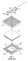
- FIG. 1is an exploded view of a known electronic apparatus 10 including a heat transfer apparatus 12 for coupling to a PGA device 14 positioned within a zero insertion force (ZIF) socket 16 .
- PGA device 14includes a PGA device package housing an integrated circuit (IC), and includes multiple pin terminals arranged across an underside surface providing input/output capability for the IC.
- Heat transfer apparatus 12includes a heat sink 18 and a spring clip 20 .
- An upper surface of heat sink 18includes multiple pins projecting upwardly and arranged in rows.
- ZIF socket 16includes multiple holes in an upper surface for receiving the pins of PGA device 14 , a handle 22 along one side for operating an internal pin coupling mechanism, and multiple pin terminals arranged across an underside surface for coupling the pin terminals of PGA device 14 to electrically conductive traces of a printed circuit board.
- ZIF socket 16also includes two latching projections 24 A and 24 B extending outwardly from opposite side surfaces.
- Spring clip 20has two apertures 26 A and 26 B dimensioned to allow respective latching projections 24 A and 24 B to pass therethrough.
- PGA device 14is mounted upon the upper surface of ZIF socket 16 . With handle 22 in a raised position, the pin terminals of PGA device 14 are inserted into corresponding holes in the upper surface of ZIF socket 16 . Handle 22 is then lowered to actuate the internal pin coupling mechanism of ZIF socket 16 .
- flip chip packagesIt is now common to mount integrated circuits to substrates using the well known controlled collapse chip connection (C 4 ) or “flip chip” techniques. Device packages including integrated circuits mounted to substrates using the flip chip method are commonly known as flip chip packages.
- FIG. 2is a cross-sectional view of a known flip chip embodiment of PGA device 14 of FIG. 1 .
- PGA device 14includes an IC 32 mounted upon an upper surface of a substrate 34 using a flip chip technique, and a cover or lid 36 secured over IC 32 .
- a layer 38 of a thermal interface materialthermally couples an upward facing backside surface of IC 32 to an underside surface of lid 36 .
- Lid 36is attached (e.g., adhesively) to the upper surface of substrate 34 about outer edges of the upper surface of substrate 34 , and at locations 40 A and 40 B in FIG. 2 .
- solder bumpsconnect a set of I/O pads on a frontside surface of IC 32 to corresponding bonding pads on the upper surface of substrate 34 .
- Substrate 34includes multiple electrical conductors connecting pins 42 to bonding pads on the upper surface of substrate 12 .
- the area of the upper surface of lid 36may be, for example, about 4 square inches. In contrast, the area of the backside surface of IC 32 , thermally coupled to lid 36 , may be about 0.3 square inches.
- the underside surface of heat sink 18(FIG. 1) is thermally coupled to the upper surface of lid 36 , the effectiveness of the transfer of heat energy from IC 32 to heat sink 18 is heavily dependent upon the thermal resistance, and the heat spreading ability, of lid 36 . Further, a substantial amount of the heat energy generated within IC 32 is conducted into substrate 34 . For heat energy within substrate 34 to reach heat sink 18 (FIG.
- the heat energymust travel through the attachment points between substrate 34 and lid 36 about the outer edges of the upper surface of substrate 34 , and at locations 40 A and 40 B in FIG. 2 .
- Heat transfer paths between a portion of substrate 34 adjacent to IC 32 and the heat sinkare thus relatively long, and include substantial distances within substrate 34 .
- the effectiveness of the transfer of heat energy from substrate 34 to heat sink 18is heavily dependent upon the thermal resistance of substrate 34 , as well as the rather uncertain thermal resistances at the attachment points between substrate 34 and lid 36 .
- a heat removal apparatus for a flip chip PGA deviceincluding a heat sink in more effective thermal communication with both the IC and the substrate of the flip chip PGA device.
- the desired heat removal apparatuswould more effectively remove heat energy both from the IC and the substrate, thereby increasing the reliability of the PGA device.
- a heat transfer apparatusfor coupling to a pin grid array (PGA) device including an integrated circuit and mounted within a socket (e.g., a zero insertion force or ZIF socket).
- the socketis mounted upon a surface of a printed circuit board (PCB) and includes two latching projections extending from opposite side surfaces.
- the heat transfer apparatusincludes a thermally conductive heat sink and a spring clip for holding the heat sink in position relative to the PGA device.
- the heat sinkmay be made from a metal (e.g., aluminum), and may have multiple structures (e.g., fins or pins) extending from an upper surface.
- the heat sinkhas an opening in an underside surface for housing the PGA device and the socket.
- the heat sinkalso has a lip surrounding the opening for thermally coupling to the PCB about the socket.
- the heat sinkalso has a pair of holes extending through the heat sink from the upper surface of the heat sink into the opening.
- the spring cliphas two side members each adapted for attaching to a different one of the two latching projections of the socket.
- Each of the pair of holes in the heat sinkis positioned to receive a different one of the side members of the spring clip.
- the holes in the heat sinkmay be separated by a distance equal to a distance between the latching projections of the socket.
- the PGA deviceincludes a substrate having a substantially flat upper surface opposite the socket.
- the integrated circuit of the PGA deviceis mounted upon the upper surface of the substrate such that the integrated circuit is elevationally raised above the upper surface of the substrate.
- the opening in the underside of the heat sinkincludes a first cavity dimensioned to receive the socket and the substrate of the PGA device.
- the first cavityhas an upper wall, and the opening also includes a second cavity in the upper wall of the first cavity. The second cavity is dimensioned to receive the integrated circuit.
- the heat transfermay include a first thermal interface layer positioned between the integrated circuit and an upper wall of the second cavity.
- the heat transfer apparatusmay also include a second thermal interface layer positioned between a region of the upper surface of the substrate surrounding the integrated circuit and an adjoining portion of the upper wall of the first cavity.
- the heat transfer apparatusmay also include a third thermal interface layer positioned about the socket between the lip of the heat sink and the surface of the PCB.
- the spring clipmay include a joining member connected between the two side members.
- the joining membermay be made from a resilient material (e.g., spring steel).
- the joining memberhas two ends and a bowed center section between the two ends.
- the two ends of the joining memberare substantially parallel to one another.
- Each side member of the spring cliphas an upper end and a lower end, and a hole in the lower end dimensioned to allow a corresponding one of the latching projections of the socket to pass therethrough.
- One of the two ends of the joining memberis connected to the upper end of one of the side members, and the other end of the joining member is connected to the upper end of the other side member.
- the center section of the joining memberis bowed toward the lower ends of the side members such that the spring clip is substantially “M”-shaped.
- the latching projections of the socketmay be substantially rectangular.
- the holes in the lower ends of the side members of the spring clipmay also be rectangular.
- the spring clipmay be formed from a single piece of resilient material (e.g., spring steel). In this case, the spring clip may have sharp bends at interfaces between the side members and the joining member.
- a method for coupling the heat sink to the PGA deviceincludes positioning the heat sink over the PGA device and the socket such that the PGA device and the socket reside in the opening in the underside surface of the heat sink.
- the lower ends of the two side members of the spring clipare inserted into the holes in the heat sink.
- the side members of the spring clipare pushed downward along the opposite side surfaces of the socket until the latching projections of the socket pass through the corresponding holes in the lower ends of the side members.
- a method for removing the spring clip holding the heat sink in positionincludes exerting a force between upper ends of two side members extending from the holes in the heat sink.
- the forcecauses the upper ends of the two side members to move toward one another, and the lower ends of the side members to move away from one another.
- the moving of the lower ends away from one anotherallows the latching projections of the socket to exit the holes in the lower ends of the side members, thus detaching the spring clip from the socket.
- FIG. 1is an exploded view of a known electronic apparatus including a heat transfer apparatus for coupling to a PGA device positioned within a zero insertion force (ZIF) socket;
- ZIFzero insertion force
- FIG. 2is a cross-sectional view of a known flip chip embodiment of the PGA device of FIG. 1;
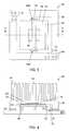
- FIG. 3is a top plan view of a heat transfer apparatus coupled to a flip chip PGA device positioned within a zero insertion force (ZIF) socket, wherein the heat transfer apparatus includes a heat sink held in place by a spring clip;
- ZIFzero insertion force
- FIG. 4is a cross-sectional view of the heat transfer apparatus of FIG. 3;
- FIG. 5is a cross-sectional view of the flip chip PGA device of FIGS. 3 and 4;
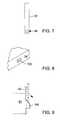
- FIG. 6is a side elevation view of one embodiment of the spring clip of FIGS. 3-4, wherein the spring clip includes two side members connected by a joining member, and wherein each of the two side members has a hole in a lower end for receiving a latching projection of the ZIF socket;
- FIG. 7is a side elevation view of one of the side members of the spring clip of FIG. 6 illustrating one embodiment of the hole in the lower end of the side member, wherein the hole is rectangular and dimensioned to receive a rectangular latching projection;
- FIG. 8is a perspective view of one embodiment of the latching projections of FIG. 6, wherein each latching projection is substantially rectangular and has a downward sloping upper surface which facilitates installation of the spring clip;
- FIG. 9is a side elevation view of a side member of the spring clip of FIG. 6 being attached to a latching projection of the ZIF socket.
- FIGS. 3 and 4will now be used to illustrate one embodiment of a heat transfer apparatus 50 for coupling to a flip chip pin grid array (PGA) device 52 , wherein flip chip PGA device 52 is positioned within a zero insertion force (ZIF) socket 54 .
- FIG. 3is a top plan view of heat transfer apparatus 50 coupled to PGA device 52
- FIG. 4is a cross-sectional view of heat transfer apparatus 50 as indicated in FIG. 3 .
- Flip chip PGA device 52includes an integrated circuit (IC) 60 mounted upon a substantially flat upper surface of a substrate 62 such that IC 60 is elevationally raised above the upper surface of substrate 62 .
- ICintegrated circuit
- Heat transfer apparatus 50includes a heat sink 56 and a spring clip 58 , and is used to transfer heat energy from IC 60 , substrate 62 , and a printed circuit board to which ZIF socket 54 is mounted, to an ambient surrounding heat transfer apparatus 50 .
- Heat sink 56has multiple pins 64 extending upwardly from an upper surface.
- ZIF socket 54includes an internal pin coupling mechanism for coupling pins 66 of PGA device 52 to corresponding pins of ZIF socket 54 .
- the pin coupling mechanismis actuated by a handle 63 along one side of ZIF socket 54 . With handle 63 in a raised position, pins 66 of PGA device 52 are inserted into the corresponding holes in the upper surface of ZIF socket 54 . Handle 63 is then lowered to actuate the internal pin coupling mechanism, thereby coupling pins 66 of PGA device 52 to corresponding pins of ZIF socket 54 , and to corresponding traces of PCB 68 .
- Substrate 62 of PGA device 52has multiple pins 66 extending downwardly from an underside surface. Pins 66 provide input/output capability for IC 60 .
- PGA device 52is positioned within ZIF socket 54 such that pins 66 extend into corresponding holes in an upper surface of ZIF socket 54 .
- ZIF socket 54is mounted upon a surface of a printed circuit board (PCB) 68 .
- PCBprinted circuit board
- ZIF socket 54may have, for example, pins extending from an underside surface and coupled to corresponding electrically conductive traces of PCB 68 .
- the pins of ZIF socket 54may extend into corresponding holes in PCB 68 .
- ZIF socket 54includes an internal pin coupling mechanism for coupling pins 66 of PGA device 52 to corresponding pins of ZIF socket 54 .
- the pin coupling mechanismis actuated by a handle 63 along one side of ZIF socket 54 . With handle 63 in a raised position, pins 66 of PGA device 52 are inserted into the corresponding holes in the upper surface of ZIF socket 54 . Handle 63 is then lowered to actuate the internal pin coupling mechanism, thereby coupling pins 66 of PGA device 52 to corresponding pins of ZIF socket 54 , and to corresponding traces of PCB 64 .
- FIG. 5is a cross-sectional view of flip chip PGA device 52 of FIGS. 3 and 4.
- IC 60is mounted upon a center portion of the upper surface of substrate 62 using the flip chip method.
- Multiple solder bumps 80connect a set of I/O pads on a frontside surface of IC 60 to corresponding bonding pads on the upper surface of substrate 62 .
- a layer 82 of an “underfill” materialseals the flip chip connections and provides other mechanical advantages.
- Substrate 62includes multiple electrical conductors 84 connecting pins 64 to bonding pads on the upper surface of substrate 62 .
- Electrical conductors 84may be disposed in a stacked arrangement within substrate 62 . As evident in FIGS. 4 and 5, an upward facing backside surface of IC 60 is at a higher elevation relative to the upper surface of substrate 62 .
- heat sink 56is positioned between PGA device 52 and the ambient during use, and held in place by spring clip 58 .
- Heat sink 56is made out of a thermally conductive material (e.g., aluminum).
- an underside surface of heat sink 56has a cavity 70 dimensioned to receive ZIF socket 54 with flip ship PGA device 52 mounted thereon.
- Cavity 70includes a substantially flat upper wall 72 .
- Upper wall 72has a cavity dimensioned to receive IC 60 of PGA device 52 .
- ZIF socket 54 and substrate 62 of PGA device 52are positioned within cavity 70 as shown in FIG. 4, and IC 60 of PGA device 52 is positioned within the cavity in upper wall 72 as shown in FIG. 4 .
- the remaining portion of the underside surface of heat sink 56forms a lip surrounding a mouth of cavity 70 .
- heat transfer apparatus 50may also include a first thermal interface layer 74 positioned between the upward facing backside surface of IC 60 and an upper wall of the cavity dimensioned to receive IC 60 .
- Thermal interface layer 74thermally couples IC 60 to heat sink 56 .
- First thermal interface layer 74is preferably made of a material which changes phase (i.e., flows) to fill air pockets between IC 60 and heat sink 56 , and to fill microscopic irregularities in contacted surfaces of IC 60 and heat sink 56 , under a relatively small amount of pressure applied between heat sink 56 and PGA device 52 .
- First thermal interface layer 74thus achieves an acceptably low value of thermal resistance between IC 60 and heat sink 56 under a relatively small amount of pressure applied between heat sink 56 and PGA device 52 .
- First thermal interface layer 74may be, for example, a layer of thermal grease or thermal wax.
- Thermal greasescontain particles of thermally conductive material (e.g., ceramic particles) suspended in a viscous silicone or hydrocarbon fluid base.
- Thermal waxescontain thermally conductive particles suspended in a wax base.
- a suitable thermal waxis the THERMFLOWTM T725 thermal wax (Chomerics Co., Woburn, Mass.).
- first thermal interface layer 74may be a piece of thermal interface tape or a thermal interface pad which changes phase to fill air pockets and microscopic irregularities under a relatively small amount of pressure.
- a suitable thermal interface tapeis the THERMATTACHTM T412 thermal interface tape (Chomerics Co., Woburn, Mass.).
- Heat transfer apparatus 50may also include a second thermal interface layer 76 positioned between a region of the upper surface of substrate 62 surrounding IC 60 and the adjoining portion of upper wall 72 of cavity 70 .
- Thermal interface layer 76thermally couples substrate 62 to heat sink 56 adjacent to IC 60 . Heat transfer paths between a portion of substrate 34 adjacent to IC 60 and heat sink 56 are thus relatively short compared to those of FIG. 2 .
- Second thermal interface layer 76is preferably made of a material which changes phase (i.e., flows) to fill air pockets between the upper surface of substrate 62 and upper wall 72 of cavity 70 , and to fill microscopic irregularities in the upper surface of substrate 62 and the surface of upper wall 72 , under a relatively small amount of pressure applied between heat sink 56 and PGA device 52 . Second thermal interface layer 76 thus achieves an acceptably low value of thermal resistance between the upper surface of substrate 62 and the surface of upper wall 72 under a relatively small amount of pressure applied between heat sink 56 and PGA device 52 .
- Second thermal interface layer 76may be, for example, a layer of thermal grease or thermal wax.
- Thermal greasescontain particles of thermally conductive material (e.g., ceramic particles) suspended in a viscous silicone or hydrocarbon fluid base.
- Thermal waxescontain thermally conductive particles suspended in a wax base.
- a suitable thermal waxis the THERMFLOWTM T725 thermal wax (Chomerics Co., Woburn, Mass.).
- second thermal interface layer 76may be a piece of thermal interface tape or a thermal interface pad which changes phase to fill air pockets and microscopic irregularities under a relatively small amount of pressure.
- a suitable thermal interface tapeis the THERMATTACHTM T412 thermal interface tape (Chomerics Co., Woburn, Mass.).
- Heat transfer apparatus 50may also include a third thermal interface layer 78 positioned between the underside surface of heat sink 56 , forming the lip around the mouth of cavity 70 , and a region of the surface of PCB 68 surrounding ZIF socket 54 .
- Thermal interface layer 78thermally couples PCB 68 to heat sink 56 adjacent to ZIF socket 54 .
- Thermal interface layer 78also forms a seal between the underside surface of heat sink 56 (i.e., the lip surrounding cavity 70 ) and PCB 68 , preventing foreign substances (e.g., water, sand, and dust) from entering cavity 70 .
- Thermal interface layer 78is preferably made of a thermally conductive, complaint material which changes shape in an elastic manner when subjected to mechanical force (i.e., under pressure).
- Thermal interface layer 78may be, for example, a layer of a thermal gap filler including ceramic particles dispersed in an elastomeric binder.
- Thermal interface layer 78may be, for example, a layer of V-THERMTM thermally conductive elastomer (Chomerics Co., Woburn, Mass.).
- heat sink 56 of heat transfer apparatus 50is in more effective thermal communication with both the IC and the substrate of a flip chip PGA device. Heat transfer apparatus 50 thus more effectively removes heat energy from IC 60 and substrate 62 , expectantly increasing the reliability of PGA device 52 over heat transfer system 12 . Further, by thermally coupling PCB 68 to heat sink 56 , heat energy conducted into PCB 68 from substrate 62 and ZIF socket 54 may be removed to the ambient by heat sink 56 , thereby expectantly increasing the reliability of PCB 68 and components mounted thereto.
- FIG. 6is a side elevation view of one embodiment of spring clip 58 of FIGS. 3-4.
- spring clip 58is substantially “M”-shaped, and includes two side members 90 A and 90 B joined by a joining member 92 having two ends and a bowed center section.
- spring clip 58is preferably made from a single piece of resilient material (e.g., spring steel).
- spring clip 58has two sharp bends 94 A and 94 B at junctions between side members 90 A and 90 B and joining member 92 where the resilient material is bent back over itself.
- the two ends of joining member 92are substantially parallel to one another. As illustrated in FIG.
- one upward pointing end of joining member 92is preferably in contact with an upper end of side member 90 A, and the other upward pointing end of joining member 92 is preferably in contact with an upper end of side member 90 B.
- the bowed center section of joining member 92diverges from the side members at points 96 A and 96 B as illustrated in FIG. 6 .
- Side members 90 A and 90 Bhave respective holes 98 A and 98 B in lower ends.
- FIG. 7is a side elevation view of one of the side members 90 of spring clip 58 of FIG. 6 illustrating one embodiment of hole 98 in the lower end of the side member 90 .
- ZIF socket 54includes two latching projections 100 A and 100 B extending outwardly from opposite side surfaces of ZIF socket 54 .
- Holes 98 A and 98 B in respective side members 90 A and 90 Bare dimensioned to allow respective latching projections 100 A and 100 B to pass therethrough.
- hole 98is rectangular and dimensioned to receive a rectangular latching projection 100 .
- heat sink 56has two holes 65 A and 65 B positioned and dimensioned to receive respective side members 90 A and 90 B of spring clip 58 .
- spring clip 58When spring clip 58 is installed such that latching projections 100 A and 100 B of ZIF socket 54 pass through respective holes 98 A and 98 B in respective side members 90 A and 90 B of spring clip 58 , the bowed center section of joining member 92 of spring clip 58 is deformed, and exerts a force between heat sink 56 and ZIF socket 54 .
- PGA device 52is positioned between heat sink 56 and ZIF socket 54 and fixed relative to ZIF socket 54 , the force exerted by spring clip 58 between heat sink 56 and ZIF socket 54 urges heat sink 56 toward PGA device 52 .
- spring clip 58serves hold heat sink 56 in place relative to PGA device 52 and to urge heat sink 56 toward PGA device 52 .
- FIG. 8is a perspective view of one embodiment of the latching projections 100 of FIG. 6 .
- each latching projection 100is substantially rectangular and has a downward sloping upper surface which facilitates installation of spring clip 58 .
- first thermal interface layer 74may be formed upon the upper wall of the cavity of heat sink 56 dimensioned to receive IC 60 of PGA device 52 . Alternately, first thermal interface layer 74 may be formed upon the upper surface of IC 60 . Similarly, second thermal interface layer 76 may be formed upon upper wall 72 of cavity 70 of heat sink 56 in the location expected to adjoin the region of the upper surface of substrate 62 surrounding IC 60 . Alternately, second thermal interface layer 76 may be formed upon the region of the upper surface of substrate 62 surrounding IC 60 . Third thermal interface layer 78 may be positioned between the underside surface of heat sink 56 and PCB 68 .
- Heat sink 56is positioned about PGA device 52 , located within ZIF socket 54 , as shown in FIGS. 3-4 such that holes 65 A and 65 B extending through heat sink 56 are vertically aligned over latching projections 100 A and 100 B of ZIF socket 54 .
- Spring clip 58is then installed to hold heat sink 56 in place relative to PGA device 52 and to urge heat sink 56 toward PGA device 52 .
- the lower ends of side members 90 A and 90 B of spring clip 58are inserted into respective holes 65 A and 65 B.
- side members 90 A and 90 B of spring clip 58are pushed downward along the side surfaces of ZIF socket 54 and the upper surfaces of respective latching projections 100 A and 100 B until latching projections 100 A and 100 B pass through respective holes 98 A and 98 B in respective side members 90 A and 90 B.
- the bowed center section of joining member 92 of spring clip 58is deformed during the installation process as described above, exerting a force between heat sink 56 and ZIF socket 54 which urges heat sink 56 toward PGA device 52 following installation.
- spring clip 58may be removed by exerting a force F between the upper ends of side members 90 A and 90 B. Force F causes the upper ends of side members 90 A and 90 B to move toward each other. Side members 90 A and 90 b pivot about respective points 96 A and 96 B as illustrated in FIG. 6 . The lower ends of side members 90 A and 90 B swing outwardly away from each other, allowing latching projections 100 A and 100 B to exit respective holes 98 A and 98 B in respective side members 90 A and 90 B. Side members 90 A and 90 B of spring clip 58 may then be extracted from corresponding holes 65 A and 65 B in heat sink 56 . Once spring clip 58 is removed, the other components of heat transfer apparatus 50 may be removed.
- heat transfer apparatus 50is not limited to embodiments where PGA device 52 is a flip chip PGA device and socket 54 is a ZIF socket.
- heat transfer apparatus 50may also be useful for removing heat energy from a PGA device having a substantially flat upper surface (e.g., PGA device 14 in FIGS. 1 and 2 ).
- heat sink 56may have a single cavity for receiving the PGA device and socket 54 , and a single thermal interface layer may be used to couple the upper surface of the PGA device to an upper wall of the single cavity of heat sink 56 .
- heat transfer apparatus 50may also be useful for removing heat energy from a PGA device positioned in, for example, a low insertion force (LIF) socket having latching projections extending outwardly from opposite side surfaces.
- LIFlow insertion force
Landscapes
- Physics & Mathematics (AREA)
- Condensed Matter Physics & Semiconductors (AREA)
- General Physics & Mathematics (AREA)
- Engineering & Computer Science (AREA)
- Computer Hardware Design (AREA)
- Microelectronics & Electronic Packaging (AREA)
- Power Engineering (AREA)
- Cooling Or The Like Of Electrical Apparatus (AREA)
- Cooling Or The Like Of Semiconductors Or Solid State Devices (AREA)
Abstract
Description
Claims (27)
Priority Applications (2)
| Application Number | Priority Date | Filing Date | Title |
|---|---|---|---|
| US09/544,749US6504243B1 (en) | 2000-04-07 | 2000-04-07 | Removable heat transfer apparatus for a pin grid array (PGA) device, and associated installation and removal methods |
| PCT/US2000/031962WO2001078143A1 (en) | 2000-04-07 | 2000-11-21 | Removable heat transfer apparatus for a pin grid array (pga) dev ice |
Applications Claiming Priority (1)
| Application Number | Priority Date | Filing Date | Title |
|---|---|---|---|
| US09/544,749US6504243B1 (en) | 2000-04-07 | 2000-04-07 | Removable heat transfer apparatus for a pin grid array (PGA) device, and associated installation and removal methods |
Publications (1)
| Publication Number | Publication Date |
|---|---|
| US6504243B1true US6504243B1 (en) | 2003-01-07 |
Family
ID=24173429
Family Applications (1)
| Application Number | Title | Priority Date | Filing Date |
|---|---|---|---|
| US09/544,749Expired - LifetimeUS6504243B1 (en) | 2000-04-07 | 2000-04-07 | Removable heat transfer apparatus for a pin grid array (PGA) device, and associated installation and removal methods |
Country Status (2)
| Country | Link |
|---|---|
| US (1) | US6504243B1 (en) |
| WO (1) | WO2001078143A1 (en) |
Cited By (33)
| Publication number | Priority date | Publication date | Assignee | Title |
|---|---|---|---|---|
| US20020075640A1 (en)* | 2000-12-18 | 2002-06-20 | Zhang Franklin Zhigang | Expandable computer board with dual shield housing solutions |
| US20020093092A1 (en)* | 2000-12-22 | 2002-07-18 | Konstantinos Kanelis | Power semiconductor module and cooling element for holding the power semiconductor module |
| US20030104652A1 (en)* | 2001-12-03 | 2003-06-05 | Vassoudevane Lebonheur | Semiconductor chip package and method of manufacturing same |
| US20040090745A1 (en)* | 2002-11-08 | 2004-05-13 | Agilent Technologies, Inc. | Cooling a microchip on a circuit board |
| US20040125570A1 (en)* | 2002-12-16 | 2004-07-01 | Amber Glenn M. | System for loading a heat sink mechanism independently of clamping load on electrical device |
| US20040190259A1 (en)* | 2003-03-31 | 2004-09-30 | Nick Labanok | Integrated heat spreader with downset edge, and method of making same |
| US6853068B1 (en)* | 2002-05-22 | 2005-02-08 | Volterra Semiconductor Corporation | Heatsinking and packaging of integrated circuit chips |
| US6870258B1 (en) | 2003-06-16 | 2005-03-22 | Advanced Micro Devices | Fixture suitable for use in coupling a lid to a substrate and method |
| US6936501B1 (en) | 2004-04-05 | 2005-08-30 | Advanced Micro Devices, Inc. | Semiconductor component and method of manufacture |
| US7056143B2 (en) | 2003-03-27 | 2006-06-06 | Hewlett-Packard Development Company, L.P. | Electronic device having removable processor assembly and method of operating same |
| US20060220226A1 (en)* | 2005-03-30 | 2006-10-05 | Intel Corporation | Integrated heat spreader with intermetallic layer and method for making |
| US20070076378A1 (en)* | 2005-09-30 | 2007-04-05 | Blanco Richard L Jr | Thermal contact arrangement |
| US20070177367A1 (en)* | 2006-02-01 | 2007-08-02 | Apple Computer, Inc. | Thermal interface apparatus |
| US7256065B1 (en) | 2004-06-03 | 2007-08-14 | Advanced Micro Devices, Inc. | Methods and fixture for coupling a lid to a support substrate |
| FR2898462A1 (en)* | 2006-03-08 | 2007-09-14 | Thales Sa | THERMAL DRAIN FOR ELECTRONIC BOARD COMPRISING GRAPHITE ELEMENTS |
| US20090034206A1 (en)* | 2006-06-30 | 2009-02-05 | Intel Corporation | Wafer-level assembly of heat spreaders for dual ihs packages |
| US20090284534A1 (en)* | 2008-05-15 | 2009-11-19 | Apple Inc. | Thermal management of graphics processing units |
| US20100103147A1 (en)* | 2008-10-28 | 2010-04-29 | Apple Inc. | Graphics controllers with increased thermal management granularity |
| US20120325454A1 (en)* | 2010-03-12 | 2012-12-27 | Fujitsu Limited | Heat dissipating structure and manufacture thereof |
| US8477490B2 (en) | 2011-05-02 | 2013-07-02 | Apple Inc. | Cooling system for mobile electronic devices |
| US8593821B2 (en)* | 2006-08-18 | 2013-11-26 | Delphi Technologies, Inc. | Lightweight audio system for automotive applications and method |
| US20140110894A1 (en)* | 2012-10-22 | 2014-04-24 | Samsung Electronics Co., Ltd. | Wafer Carrier Having Cavity |
| US20140237815A1 (en)* | 2013-02-25 | 2014-08-28 | Advanced Micro Devices, Inc. | Stiffener frame fixture |
| US9066446B1 (en)* | 2012-02-22 | 2015-06-23 | SeeScan, Inc. | Thermal extraction architecture for camera heads, inspection systems, and other devices and systems |
| US9125299B2 (en) | 2012-12-06 | 2015-09-01 | Apple Inc. | Cooling for electronic components |
| US9223167B2 (en) | 2013-06-26 | 2015-12-29 | Apple Inc. | Liquid crystal switching barrier thermal control |
| US9389029B2 (en) | 2013-09-30 | 2016-07-12 | Apple Inc. | Heat transfer structure |
| US9674986B2 (en) | 2015-08-03 | 2017-06-06 | Apple Inc. | Parallel heat spreader |
| US9818669B2 (en) | 2014-08-06 | 2017-11-14 | Honeywell International Inc. | Printed circuit board assembly including conductive heat transfer |
| US9888602B2 (en) | 2012-09-24 | 2018-02-06 | Coriant Oy | Circuit board system comprising a spring fastened element |
| US20230125822A1 (en)* | 2021-10-27 | 2023-04-27 | Intel Corporation | Immersion cooling for integrated circuit devices |
| US20240422922A1 (en)* | 2023-06-16 | 2024-12-19 | Aptiv Technologies AG | Joining Element For A Housing |
| US12301744B2 (en) | 2022-01-10 | 2025-05-13 | Apple Inc. | Handheld electronic device |
Citations (12)
| Publication number | Priority date | Publication date | Assignee | Title |
|---|---|---|---|---|
| US5357404A (en) | 1991-11-18 | 1994-10-18 | The Whitaker Corporation | EMI shield, and assembly using same |
| DE4338393A1 (en) | 1993-11-10 | 1995-05-11 | Philips Patentverwaltung | Arrangement for dissipating heat from (cooling) an electronic component soldered onto a printed circuit board |
| US5552635A (en)* | 1994-01-11 | 1996-09-03 | Samsung Electronics Co., Ltd. | High thermal emissive semiconductor device package |
| US5585671A (en)* | 1994-10-07 | 1996-12-17 | Nagesh; Voddarahalli K. | Reliable low thermal resistance package for high power flip clip ICs |
| US5594624A (en) | 1994-04-05 | 1997-01-14 | Thermalloy, Inc. | Strap spring for heat sink clip assembly |
| US5651688A (en) | 1995-12-20 | 1997-07-29 | Lin; Chuen-Sheng | Apparatus for mounting CPU heat dissipator |
| US5745344A (en)* | 1995-11-06 | 1998-04-28 | International Business Machines Corporation | Heat dissipation apparatus and method for attaching a heat dissipation apparatus to an electronic device |
| US5777852A (en) | 1995-07-20 | 1998-07-07 | Bell; James S. | Clamping device for securing an electrical component to a circuit board |
| US5847928A (en)* | 1996-07-09 | 1998-12-08 | Thermalloy, Inc. | Strap spring for attaching heat sinks to circuit boards |
| US5907474A (en)* | 1997-04-25 | 1999-05-25 | Advanced Micro Devices, Inc. | Low-profile heat transfer apparatus for a surface-mounted semiconductor device employing a ball grid array (BGA) device package |
| US5990552A (en) | 1997-02-07 | 1999-11-23 | Intel Corporation | Apparatus for attaching a heat sink to the back side of a flip chip package |
| US6108207A (en)* | 1999-06-29 | 2000-08-22 | Foxconn Precision Components Co., Ltd. | Clip for heat sink |
- 2000
- 2000-04-07USUS09/544,749patent/US6504243B1/ennot_activeExpired - Lifetime
- 2000-11-21WOPCT/US2000/031962patent/WO2001078143A1/enactiveApplication Filing
Patent Citations (13)
| Publication number | Priority date | Publication date | Assignee | Title |
|---|---|---|---|---|
| US5357404A (en) | 1991-11-18 | 1994-10-18 | The Whitaker Corporation | EMI shield, and assembly using same |
| DE4338393A1 (en) | 1993-11-10 | 1995-05-11 | Philips Patentverwaltung | Arrangement for dissipating heat from (cooling) an electronic component soldered onto a printed circuit board |
| US5552635A (en)* | 1994-01-11 | 1996-09-03 | Samsung Electronics Co., Ltd. | High thermal emissive semiconductor device package |
| US5594624A (en) | 1994-04-05 | 1997-01-14 | Thermalloy, Inc. | Strap spring for heat sink clip assembly |
| US5585671A (en)* | 1994-10-07 | 1996-12-17 | Nagesh; Voddarahalli K. | Reliable low thermal resistance package for high power flip clip ICs |
| US5850691A (en) | 1995-07-20 | 1998-12-22 | Dell Usa, L. P. | Method for securing an electronic component to a pin grid array socket |
| US5777852A (en) | 1995-07-20 | 1998-07-07 | Bell; James S. | Clamping device for securing an electrical component to a circuit board |
| US5745344A (en)* | 1995-11-06 | 1998-04-28 | International Business Machines Corporation | Heat dissipation apparatus and method for attaching a heat dissipation apparatus to an electronic device |
| US5651688A (en) | 1995-12-20 | 1997-07-29 | Lin; Chuen-Sheng | Apparatus for mounting CPU heat dissipator |
| US5847928A (en)* | 1996-07-09 | 1998-12-08 | Thermalloy, Inc. | Strap spring for attaching heat sinks to circuit boards |
| US5990552A (en) | 1997-02-07 | 1999-11-23 | Intel Corporation | Apparatus for attaching a heat sink to the back side of a flip chip package |
| US5907474A (en)* | 1997-04-25 | 1999-05-25 | Advanced Micro Devices, Inc. | Low-profile heat transfer apparatus for a surface-mounted semiconductor device employing a ball grid array (BGA) device package |
| US6108207A (en)* | 1999-06-29 | 2000-08-22 | Foxconn Precision Components Co., Ltd. | Clip for heat sink |
Non-Patent Citations (1)
| Title |
|---|
| International Search Report, application No. PCT/US 00/31962, mailed Apr. 26, 2001. |
Cited By (52)
| Publication number | Priority date | Publication date | Assignee | Title |
|---|---|---|---|---|
| US20020075640A1 (en)* | 2000-12-18 | 2002-06-20 | Zhang Franklin Zhigang | Expandable computer board with dual shield housing solutions |
| US7061774B2 (en)* | 2000-12-18 | 2006-06-13 | Franklin Zhigang Zhang | Computer board with dual shield housing and heat sink expansion zone apparatuses |
| US20020093092A1 (en)* | 2000-12-22 | 2002-07-18 | Konstantinos Kanelis | Power semiconductor module and cooling element for holding the power semiconductor module |
| US6791183B2 (en)* | 2000-12-22 | 2004-09-14 | Infineon Technologies Ag | Power semiconductor module and cooling element for holding the power semiconductor module |
| US20030104652A1 (en)* | 2001-12-03 | 2003-06-05 | Vassoudevane Lebonheur | Semiconductor chip package and method of manufacturing same |
| US6975025B2 (en)* | 2001-12-03 | 2005-12-13 | Intel Corporation | Semiconductor chip package and method of manufacturing same |
| US6853068B1 (en)* | 2002-05-22 | 2005-02-08 | Volterra Semiconductor Corporation | Heatsinking and packaging of integrated circuit chips |
| US6963130B1 (en)* | 2002-05-22 | 2005-11-08 | Volterra Semiconductor Corporation | Heatsinking and packaging of integrated circuit chips |
| US20040090745A1 (en)* | 2002-11-08 | 2004-05-13 | Agilent Technologies, Inc. | Cooling a microchip on a circuit board |
| US6809930B2 (en)* | 2002-11-08 | 2004-10-26 | Agilent Technologies Inc. | Cooling a microchip on a circuit board |
| US7242583B2 (en)* | 2002-12-16 | 2007-07-10 | Paricon Technologies, Corporation | System for loading a heat sink mechanism independently of clamping load on electrical device |
| US20040125570A1 (en)* | 2002-12-16 | 2004-07-01 | Amber Glenn M. | System for loading a heat sink mechanism independently of clamping load on electrical device |
| US7056143B2 (en) | 2003-03-27 | 2006-06-06 | Hewlett-Packard Development Company, L.P. | Electronic device having removable processor assembly and method of operating same |
| US20050212123A1 (en)* | 2003-03-31 | 2005-09-29 | Intel Corporation | Integrated heat spreader with downset edge, and method of making same |
| US6882535B2 (en)* | 2003-03-31 | 2005-04-19 | Intel Corporation | Integrated heat spreader with downset edge, and method of making same |
| US20040190259A1 (en)* | 2003-03-31 | 2004-09-30 | Nick Labanok | Integrated heat spreader with downset edge, and method of making same |
| US6870258B1 (en) | 2003-06-16 | 2005-03-22 | Advanced Micro Devices | Fixture suitable for use in coupling a lid to a substrate and method |
| US6936501B1 (en) | 2004-04-05 | 2005-08-30 | Advanced Micro Devices, Inc. | Semiconductor component and method of manufacture |
| US7256065B1 (en) | 2004-06-03 | 2007-08-14 | Advanced Micro Devices, Inc. | Methods and fixture for coupling a lid to a support substrate |
| US7485495B2 (en) | 2005-03-30 | 2009-02-03 | Intel Corporation | Integrated heat spreader with intermetallic layer and method for making |
| US20060220226A1 (en)* | 2005-03-30 | 2006-10-05 | Intel Corporation | Integrated heat spreader with intermetallic layer and method for making |
| US7183641B2 (en) | 2005-03-30 | 2007-02-27 | Intel Corporation | Integrated heat spreader with intermetallic layer and method for making |
| US20070076378A1 (en)* | 2005-09-30 | 2007-04-05 | Blanco Richard L Jr | Thermal contact arrangement |
| US8215012B2 (en) | 2005-09-30 | 2012-07-10 | Apple Inc. | Thermal contact arrangement |
| US20090044407A1 (en)* | 2005-09-30 | 2009-02-19 | Apple Inc. | Thermal contact arrangement |
| US7433191B2 (en)* | 2005-09-30 | 2008-10-07 | Apple Inc. | Thermal contact arrangement |
| US7440281B2 (en) | 2006-02-01 | 2008-10-21 | Apple Inc. | Thermal interface apparatus |
| US20070177367A1 (en)* | 2006-02-01 | 2007-08-02 | Apple Computer, Inc. | Thermal interface apparatus |
| FR2898462A1 (en)* | 2006-03-08 | 2007-09-14 | Thales Sa | THERMAL DRAIN FOR ELECTRONIC BOARD COMPRISING GRAPHITE ELEMENTS |
| US20090034206A1 (en)* | 2006-06-30 | 2009-02-05 | Intel Corporation | Wafer-level assembly of heat spreaders for dual ihs packages |
| US8593821B2 (en)* | 2006-08-18 | 2013-11-26 | Delphi Technologies, Inc. | Lightweight audio system for automotive applications and method |
| US20090284534A1 (en)* | 2008-05-15 | 2009-11-19 | Apple Inc. | Thermal management of graphics processing units |
| US8525840B2 (en) | 2008-05-15 | 2013-09-03 | Apple Inc. | Thermal management of graphics processing units |
| US9063713B2 (en) | 2008-10-28 | 2015-06-23 | Apple Inc. | Graphics controllers with increased thermal management granularity |
| US20100103147A1 (en)* | 2008-10-28 | 2010-04-29 | Apple Inc. | Graphics controllers with increased thermal management granularity |
| US20120325454A1 (en)* | 2010-03-12 | 2012-12-27 | Fujitsu Limited | Heat dissipating structure and manufacture thereof |
| US20180158753A1 (en)* | 2010-03-12 | 2018-06-07 | Fujitsu Limited | Heat dissipating structure and manufacture |
| US8477490B2 (en) | 2011-05-02 | 2013-07-02 | Apple Inc. | Cooling system for mobile electronic devices |
| US9066446B1 (en)* | 2012-02-22 | 2015-06-23 | SeeScan, Inc. | Thermal extraction architecture for camera heads, inspection systems, and other devices and systems |
| US9888602B2 (en) | 2012-09-24 | 2018-02-06 | Coriant Oy | Circuit board system comprising a spring fastened element |
| US9583373B2 (en)* | 2012-10-22 | 2017-02-28 | Samsung Electronics Co., Ltd. | Wafer carrier having cavity |
| US20140110894A1 (en)* | 2012-10-22 | 2014-04-24 | Samsung Electronics Co., Ltd. | Wafer Carrier Having Cavity |
| US9125299B2 (en) | 2012-12-06 | 2015-09-01 | Apple Inc. | Cooling for electronic components |
| US9349628B2 (en)* | 2013-02-25 | 2016-05-24 | Advanced Micro Devices, Inc. | Method and an alignment plate for engaging a stiffener frame and a circuit board |
| US20140237815A1 (en)* | 2013-02-25 | 2014-08-28 | Advanced Micro Devices, Inc. | Stiffener frame fixture |
| US9223167B2 (en) | 2013-06-26 | 2015-12-29 | Apple Inc. | Liquid crystal switching barrier thermal control |
| US9389029B2 (en) | 2013-09-30 | 2016-07-12 | Apple Inc. | Heat transfer structure |
| US9818669B2 (en) | 2014-08-06 | 2017-11-14 | Honeywell International Inc. | Printed circuit board assembly including conductive heat transfer |
| US9674986B2 (en) | 2015-08-03 | 2017-06-06 | Apple Inc. | Parallel heat spreader |
| US20230125822A1 (en)* | 2021-10-27 | 2023-04-27 | Intel Corporation | Immersion cooling for integrated circuit devices |
| US12301744B2 (en) | 2022-01-10 | 2025-05-13 | Apple Inc. | Handheld electronic device |
| US20240422922A1 (en)* | 2023-06-16 | 2024-12-19 | Aptiv Technologies AG | Joining Element For A Housing |
Also Published As
| Publication number | Publication date |
|---|---|
| WO2001078143A1 (en) | 2001-10-18 |
Similar Documents
| Publication | Publication Date | Title |
|---|---|---|
| US6504243B1 (en) | Removable heat transfer apparatus for a pin grid array (PGA) device, and associated installation and removal methods | |
| US5990552A (en) | Apparatus for attaching a heat sink to the back side of a flip chip package | |
| KR100312236B1 (en) | Integral design features for heatsink attach for electronic packages | |
| US5907474A (en) | Low-profile heat transfer apparatus for a surface-mounted semiconductor device employing a ball grid array (BGA) device package | |
| US6078500A (en) | Pluggable chip scale package | |
| US6862186B2 (en) | Stack up assembly | |
| US5926371A (en) | Heat transfer apparatus which accommodates elevational disparity across an upper surface of a surface-mounted semiconductor device | |
| US6614659B2 (en) | De-mountable, solderless in-line lead module package with interface | |
| US6297960B1 (en) | Heat sink with alignment and retaining features | |
| TW541675B (en) | Stacked semiconductor device assembly with microelectronic spring contacts | |
| US5561594A (en) | Circuit connection in an electrical assembly | |
| US6320397B1 (en) | Molded plastic carrier for testing semiconductor dice | |
| US5940271A (en) | Stiffener with integrated heat sink attachment | |
| US5006924A (en) | Heat sink for utilization with high density integrated circuit substrates | |
| US5917703A (en) | Integrated circuit intercoupling component with heat sink | |
| US6545871B1 (en) | Apparatus for providing heat dissipation for a circuit element | |
| EP1732130A2 (en) | Circuit assembly with surface-mount IC package and heat sink | |
| US6256202B1 (en) | Integrated circuit intercoupling component with heat sink | |
| US7255571B2 (en) | Temperature dependent semiconductor module connectors | |
| US20030085453A1 (en) | Flip chip semiconductor devices and heat sink assemblies, and the coupling thereof to form an electronic apparatus including a compliant support for supporting a heat sink | |
| US7324344B2 (en) | Techniques for attaching a heatsink to a circuit board using anchors which install from an underside of the circuit board |
Legal Events
| Date | Code | Title | Description |
|---|---|---|---|
| AS | Assignment | Owner name:ADVANCED MICRO DEVICES, INC., CALIFORNIA Free format text:ASSIGNMENT OF ASSIGNORS INTEREST;ASSIGNORS:ANDRIC, ANTHONY;EYMAN, LEWIS M.;REEL/FRAME:010707/0197 Effective date:20000403 | |
| STCF | Information on status: patent grant | Free format text:PATENTED CASE | |
| FPAY | Fee payment | Year of fee payment:4 | |
| AS | Assignment | Owner name:GLOBALFOUNDRIES INC., CAYMAN ISLANDS Free format text:AFFIRMATION OF PATENT ASSIGNMENT;ASSIGNOR:ADVANCED MICRO DEVICES, INC.;REEL/FRAME:023119/0083 Effective date:20090630 | |
| FPAY | Fee payment | Year of fee payment:8 | |
| FPAY | Fee payment | Year of fee payment:12 | |
| AS | Assignment | Owner name:WILMINGTON TRUST, NATIONAL ASSOCIATION, DELAWARE Free format text:SECURITY AGREEMENT;ASSIGNOR:GLOBALFOUNDRIES INC.;REEL/FRAME:049490/0001 Effective date:20181127 | |
| AS | Assignment | Owner name:GLOBALFOUNDRIES INC., CAYMAN ISLANDS Free format text:RELEASE BY SECURED PARTY;ASSIGNOR:WILMINGTON TRUST, NATIONAL ASSOCIATION;REEL/FRAME:054636/0001 Effective date:20201117 | |
| AS | Assignment | Owner name:GLOBALFOUNDRIES U.S. INC., NEW YORK Free format text:RELEASE BY SECURED PARTY;ASSIGNOR:WILMINGTON TRUST, NATIONAL ASSOCIATION;REEL/FRAME:056987/0001 Effective date:20201117 |