US6504141B1 - Adaptive amplifier circuit with enhanced dynamic range - Google Patents
Adaptive amplifier circuit with enhanced dynamic rangeDownload PDFInfo
- Publication number
- US6504141B1 US6504141B1US09/675,483US67548300AUS6504141B1US 6504141 B1US6504141 B1US 6504141B1US 67548300 AUS67548300 AUS 67548300AUS 6504141 B1US6504141 B1US 6504141B1
- Authority
- US
- United States
- Prior art keywords
- circuit
- capacitor
- transistor
- input transistor
- input
- Prior art date
- Legal status (The legal status is an assumption and is not a legal conclusion. Google has not performed a legal analysis and makes no representation as to the accuracy of the status listed.)
- Expired - Lifetime
Links
Images


Classifications
- H—ELECTRICITY
- H04—ELECTRIC COMMUNICATION TECHNIQUE
- H04N—PICTORIAL COMMUNICATION, e.g. TELEVISION
- H04N25/00—Circuitry of solid-state image sensors [SSIS]; Control thereof
- H04N25/60—Noise processing, e.g. detecting, correcting, reducing or removing noise
- H04N25/67—Noise processing, e.g. detecting, correcting, reducing or removing noise applied to fixed-pattern noise, e.g. non-uniformity of response
- H—ELECTRICITY
- H04—ELECTRIC COMMUNICATION TECHNIQUE
- H04N—PICTORIAL COMMUNICATION, e.g. TELEVISION
- H04N25/00—Circuitry of solid-state image sensors [SSIS]; Control thereof
- H04N25/70—SSIS architectures; Circuits associated therewith
- H04N25/76—Addressed sensors, e.g. MOS or CMOS sensors
- H04N25/77—Pixel circuitry, e.g. memories, A/D converters, pixel amplifiers, shared circuits or shared components
- H—ELECTRICITY
- H10—SEMICONDUCTOR DEVICES; ELECTRIC SOLID-STATE DEVICES NOT OTHERWISE PROVIDED FOR
- H10F—INORGANIC SEMICONDUCTOR DEVICES SENSITIVE TO INFRARED RADIATION, LIGHT, ELECTROMAGNETIC RADIATION OF SHORTER WAVELENGTH OR CORPUSCULAR RADIATION
- H10F39/00—Integrated devices, or assemblies of multiple devices, comprising at least one element covered by group H10F30/00, e.g. radiation detectors comprising photodiode arrays
- H10F39/10—Integrated devices
- H10F39/12—Image sensors
- H10F39/18—Complementary metal-oxide-semiconductor [CMOS] image sensors; Photodiode array image sensors
- H10F39/184—Infrared image sensors
- H10F39/1843—Infrared image sensors of the hybrid type
Definitions
- the present inventionrelates to interface circuits for focal plane arrays (FPAs) and, specifically, to an adaptive amplifier circuit that uniquely provides high charge-handling capacity for coupling long wavelength IR detectors to multiplexing readouts with both maximum sensitivity and enhanced dynamic range.
- FPAsfocal plane arrays
- NIRnear infrared
- SWIRshort wavelength IR
- MWIRmedium wavelength IR
- LWIRlong wavelength IR
- Detectors operating in the preferred long wavelength infrared (LWIR) spectral bandcan attain the same or greater thermal sensitivity with reduced signal processing complexity. This is especially true in the 8 to 12 ⁇ m wavelength atmospheric window, which is optimum for imaging many terrestrial scenes. As a result, infrared detection and tracking can be accomplished using smaller, more cost-effective sensors having LWIR focal plane arrays.
- LWIRlong wavelength infrared
- each pixelhas an preamplifier to couple the signal from each detector into the respective unit cell.
- the corresponding readout sitemust perform several functions that are difficult to simultaneously incorporate in the small amount of “real estate” typically available on such a signal-processing chip.
- each detector/amplifier cell of an FPAshould include the following: 1) a detector interface stage that provides low impedance at a uniform operating bias; 2) an integration capacitor with large charge-handling capability; 3) a stage for uniform suppression of the background if integration capacity is inadequate; 4) facility for low-power multiplexing and reset; 5) an output buffer capable of driving the bus line capacitance for subsequent multiplexing of the electrical signal at video rates; and 6) a sufficiently large transimpedance to enable sensor-limited rather than camera-noise-limited performance; i.e., the output-referred noise level of the shot noise at the lowest background must be easily measurable by conventional camera electronics.
- U.S. Pat. No. 5,128,534teaches the technique of biasing a capacitor with a variable voltage source to increase the amount of charge that can be effectively integrated on an integrating capacitor (of the typical size that can readily fit into a standard unit cell). This improves the signal-to-noise ratio of the focal plane array by clipping excess signal.
- the enhancement in capacityis a trade-off for a nonlinear dynamic range; this non-linearity is not optimum for LWIR imaging since the signal of interest is a small fraction of the background radiation.
- U.S. Pat. No. 5,055,667 and U.S. Pat. No. RE34,802also disclose nonlinear techniques for visible CCD imagers. These methods control the dynamic range of a CCD in a manner somewhat analogous to U.S. Pat. No. 5,128,534 by providing a sink region to dispose of excess charge from the photogate region by clipping any signal above the potential set by a control gate where the potential can be similarly modulated during the exposure period. Such predetermined fluctuation can facilitate various transfer functions including logarithmic behavior. Such characteristics are not optimum for LWIR imaging.
- U.S. Pat. No. 5,382,977proposes an alternative that effectively enhances the linear charge-handling capacity via electronic scanning. Since the total charges accumulated during a typical frame time ( ⁇ fraction (1/60) ⁇ th second) can exceed 10 10 carriers while the typical integration capacitor can only handle on the order of mid-10 7 carriers, this method accepts the ⁇ 100 ⁇ disparity between the two to extend the linear capacity to approximately 10 9 carriers. Unfortunately, all the available charges for each frame time are not used so maximum sensitivity is impossible. The inefficiency translates to a proportional reduction in the effective quantum efficiency of the imaging sensor.
- U.S. Pat. No. 5,146,302again teaches skimming in a CCD to enhance the linear charge-handling capacity.
- a sampling circuitcomprising a tandem input is used to generate a prescribed skimming voltage.
- the non-uniformity in threshold voltages between the input gates of the main input and the sampling inputsets a limit on the amount of charge that can be skimmed. This limit is typically no more than 3 times the instantaneous charge-handling capacity.
- the linear capacityis thus effectively increased to the order of 10 8 carriers. A further improvement of two orders of magnitude is still needed.
- U.S. Pat. No. 6.064,431discloses a circuit for skimming to linearly enhance the effective charge-handling capacity.
- This circuitshown in FIG. 1, provides automatic control of the skimming charges to be transferred.
- the capability for predetermined sinking of excess signalas taught by U.S. patents '534, '667 and '802 noted above, is combined with conventional skimming, as taught by the '302 patent, to further enhance the effective charge-handling capacity.
- the 2 ⁇ to 3 ⁇ enhancement of '302 patentcan be enhanced to yield several orders of magnitude enhancement in charge-handling capacity. Unfortunately, the improvement is again non-linear and thus not optimum for infrared applications.
- the present inventionprovides an adaptive amplifier circuit, having minimal excess noise and a linear charge-handling capacity exceeding 10 10 electrons, to enable high-quality imaging at long wavelength infrared backgrounds and video frame rates.
- the present inventionsupports various types of photovoltaic and photoconductive detectors, and largely reduces the fixed pattern noise relative to the prior art. Since the circuit does not discriminate between dark current and photocurrent, it can also be used to operate MWIR detectors at elevated operating temperatures including room temperature.
- the adaptive detector amplifier circuitcomprises either impedance-buffered or direct injection detector interface with self-nulling skimming of the background signal and self-adapting offset suppression. An adaptive skimming circuit skims off excess charge during the integration of charge on an integration capacitor.
- This solutionfits into the typical pixel pitches normally used for single-photon detection ( ⁇ 20 ⁇ m) to amplify the photo-generated signal for subsequent processing or display.
- the resulting videohas large margin over the background noise of the camera electronics.
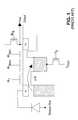
- FIG. 1is a schematic diagram of a prior art technique for enhancing dynamic range as shown in U.S. Pat. No. 6,064,431;
- FIG. 2is a schematic diagram for a preferred embodiment of an enhanced adaptive amplifier circuit with minimal noise input
- FIG. 3is a schematic diagram for an adaptive amplifier circuit with minimal noise input and impedance-buffered interface to the photodetector.
- FIG. 4is a cross-section plan for an alternative embodiment of the invention to facilitate highest performance by vertically integrating the amplifier circuit.
- the present inventionprovides a high-performance detector amplifier to support each pixel of an infrared focal plane array.
- one benefit of the various features of the present inventionis the simultaneous achievement of very high sensitivity with extended dynamic range of at least 14 bits.
- a second benefitis an output signal that is rich with signal content rather than parasitic nonuniformities.
- the usable dynamic range of most high-performance thermal imagesis limited by the fixed pattern noise arising from offset variations in the detector and amplifier.
- the amplifier circuit 2comprises a detector PD 1 that is directly coupled to the source of an input transistor Q 20 .
- the gate of Q 20is adjusted to set the detector bias and the source of Q 20 is modulated by the photo-generated signal from PD 1 .
- Minority carriersare injected into an integration capacitor C int in the adaptive skimming circuit, where they are accumulated for subsequent readout.
- the integration capacitor C intis preferably formed using a MOSFET having its source and drain connected.
- the adaptive skimming circuit 200skims off excess charge during the integration of charge on an integration capacitor.
- a suitable adaptive skimming circuitis disclosed in, for example, U.S. patent application Ser. No. 09/675,278, entitled “SELF-ADJUSTING ADAPTIVE MINIMAL NOISE INPUT AMPLIFIER CIRCUIT”, filed Sep. 29, 2000, the disclosure of which is herein incorporated by reference.
- An integration capacitor C int in the adaptive skimming circuit 200is connected to a switched-capacitor low-pass filter comprising transistors Q 30 and Q 31 , and capacitors C filter and C out .
- the signal ⁇ filterwhich is a clock that essentially parses the frame time into N integration periods, is applied to the gate of Q 30 to successively sample the signal charges integrated in C int onto C filter .
- the charge on C filteris then shared over to the output capacitor C out . Since C filter is relatively small, a smaller fraction of the charge is stored onto C out .
- This cycleis repeated N times during the frame time so that the cumulative voltage on C out exponentially reaches equilibrium. While the signal builds exponentially as described, the associated noise also adds exponentially, but in quadrature.
- ⁇C filter C filter + C int + C out C out + C filter - C filter C filter + C int ⁇ C out C out + C filter
- N boost , total⁇ N boost 1 ⁇ N boost 2 ⁇ ⁇ 10 ⁇ 1 - ⁇ N 1 + ⁇ N ⁇ 1 + ⁇ 1 - ⁇
- a source follower transistor Q 24buffers the signal and an access transistor Q 25 supplies the signal to the bus.
- a common current source CS 1may be connected to the bus and shared by all the pixels on the bus.
- FIG. 3is a schematic circuit of an alternative embodiment for use with lower impedance detectors PD 2 , such as those fabricated in the HgCdTe ternary system for operation at cutoff wavelengths beyond 12 ⁇ m at operating temperatures above 60 K.
- the negative feedback provided by amplifier 500enhances the injection efficiency of detector current into the integration capacitor C int by decreasing the input impedance of source-modulated transistor Q 520 .
- the inverting amplifiercan be of many types known to those of ordinary skill in the art, such as a basic CMOS inverter, a basic differential amplifier, or a folded cascode differential amplifier, among others. Regardless, the amplifier will also luminesce and must be optically shielded for proper operation of the skimming input circuit.
- FIG. 4is a cross-section plan where the vertical integration is achieved by combining the circuit integration provided by bulk CMOS with SOI CMOS. A part of the circuit is incorporated in the bulk CMOS constituent. The other part of the circuit is incorporated in the SOI CMOS wafer. The SOI CMOS wafer is subsequently filcher processed to remove the handle wafer. The thinned SOI material is subsequently transferred by thin-film transfer such as taught in U.S. Pat. No. 5,627,112, herein incorporated by reference.
Landscapes
- Engineering & Computer Science (AREA)
- Multimedia (AREA)
- Signal Processing (AREA)
- Transforming Light Signals Into Electric Signals (AREA)
- Solid State Image Pick-Up Elements (AREA)
- Amplifiers (AREA)
Abstract
Description


Claims (11)
Priority Applications (5)
| Application Number | Priority Date | Filing Date | Title |
|---|---|---|---|
| US09/675,483US6504141B1 (en) | 2000-09-29 | 2000-09-29 | Adaptive amplifier circuit with enhanced dynamic range |
| PCT/US2001/029306WO2002029895A1 (en) | 2000-09-29 | 2001-09-19 | Adaptive amplifier circuit with enhanced dynamic range |
| EP01971208AEP1323192B1 (en) | 2000-09-29 | 2001-09-19 | Adaptive amplifier circuit with enhanced dynamic range |
| DE60138632TDE60138632D1 (en) | 2000-09-29 | 2001-09-19 | ADAPTIVE AMPLIFIER CIRCUIT WITH IMPROVED DYNAMIC SCOPE |
| AT01971208TATE430989T1 (en) | 2000-09-29 | 2001-09-19 | ADAPTIVE AMPLIFIER CIRCUIT WITH IMPROVED DYNAMIC RANGE |
Applications Claiming Priority (1)
| Application Number | Priority Date | Filing Date | Title |
|---|---|---|---|
| US09/675,483US6504141B1 (en) | 2000-09-29 | 2000-09-29 | Adaptive amplifier circuit with enhanced dynamic range |
Publications (1)
| Publication Number | Publication Date |
|---|---|
| US6504141B1true US6504141B1 (en) | 2003-01-07 |
Family
ID=24710690
Family Applications (1)
| Application Number | Title | Priority Date | Filing Date |
|---|---|---|---|
| US09/675,483Expired - LifetimeUS6504141B1 (en) | 2000-09-29 | 2000-09-29 | Adaptive amplifier circuit with enhanced dynamic range |
Country Status (5)
| Country | Link |
|---|---|
| US (1) | US6504141B1 (en) |
| EP (1) | EP1323192B1 (en) |
| AT (1) | ATE430989T1 (en) |
| DE (1) | DE60138632D1 (en) |
| WO (1) | WO2002029895A1 (en) |
Cited By (19)
| Publication number | Priority date | Publication date | Assignee | Title |
|---|---|---|---|---|
| US20050068439A1 (en)* | 2003-09-30 | 2005-03-31 | Innovative Technology Licensing, Llc | CMOS imaging system with low fixed pattern noise |
| US20050068438A1 (en)* | 2003-09-30 | 2005-03-31 | Innovative Technology Licensing, Llc | Low noise CMOS amplifier for imaging sensors |
| US20060164530A1 (en)* | 2005-01-21 | 2006-07-27 | Bae Systems Information And Electronic Systems Integration Inc. | Dynamic range extension for focal plane arrays |
| US20070153109A1 (en)* | 2005-11-24 | 2007-07-05 | Stmicroelectronics S.A. | Image sensor element with multiple outputs |
| US20080074524A1 (en)* | 2006-08-29 | 2008-03-27 | Micron Technology, Inc. | Skimmed charge capture and charge packet removal for increased effective pixel photosensor full well capacity |
| US20080074523A1 (en)* | 2006-08-29 | 2008-03-27 | Micron Technology, Inc. | In-pixel analog memory with non-destructive read sense circuit for high dynamic range global shutter pixel operation |
| US20080218602A1 (en)* | 2007-03-07 | 2008-09-11 | Altasens, Inc. | Method and apparatus for improving and controlling dynamic range in an image sensor |
| US20090072121A1 (en)* | 2007-09-14 | 2009-03-19 | Commissariat A L'energie Atomique | Device for detecting an electromagnetic radiation with current limitation |
| US20100207028A1 (en)* | 2007-05-04 | 2010-08-19 | Thales | Laser-Pulse Matrix Detector with Rapid Summation |
| US20110063483A1 (en)* | 2009-09-16 | 2011-03-17 | Altasens, Inc. | Image sensor with wide dynamic range |
| US8415623B2 (en) | 2010-11-23 | 2013-04-09 | Raytheon Company | Processing detector array signals using stacked readout integrated circuits |
| US8637800B2 (en) | 2011-04-19 | 2014-01-28 | Altasens, Inc. | Image sensor with hybrid heterostructure |
| US20140117205A1 (en)* | 2011-04-13 | 2014-05-01 | Lg Innotek Co., Ltd. | Pixel, pixel array, image sensor including pixel array, and method of driving pixel array |
| US20160029012A1 (en)* | 2013-04-05 | 2016-01-28 | Koninklijke Philips N.V. | Re-targeting a three-dimensional image signal |
| US9998698B1 (en) | 2017-02-01 | 2018-06-12 | Omnivision Technologies, Inc. | Circuitry and method for readout of hybrid-bonded image sensors |
| US10136084B1 (en)* | 2017-10-06 | 2018-11-20 | Omnivision Technologies, Inc. | HDR skimming photodiode with true LED flicker mitigation |
| US10263031B2 (en) | 2017-02-01 | 2019-04-16 | Omnivision Technologies, Inc. | Feedback capacitor and method for readout of hybrid bonded image sensors |
| CN109709373A (en)* | 2018-12-24 | 2019-05-03 | 内蒙古电力(集团)有限责任公司电力调度控制分公司 | A kind of signal adaptive Acquisition Circuit and acquisition method |
| US10375338B2 (en) | 2017-02-01 | 2019-08-06 | Omnivision Technologies, Inc. | Two stage amplifier readout circuit in pixel level hybrid bond image sensors |
Families Citing this family (5)
| Publication number | Priority date | Publication date | Assignee | Title |
|---|---|---|---|---|
| US6504141B1 (en)* | 2000-09-29 | 2003-01-07 | Rockwell Science Center, Llc | Adaptive amplifier circuit with enhanced dynamic range |
| JP2005227214A (en)* | 2004-02-16 | 2005-08-25 | Matsushita Electric Ind Co Ltd | Angular velocity sensor and automobile using the same |
| US7821560B2 (en)* | 2005-04-07 | 2010-10-26 | Tohoku Universityu | Optical sensor, solid-state imaging device, and operating method of solid-state imaging device |
| US8625010B2 (en) | 2008-05-02 | 2014-01-07 | Canon Kabushiki Kaisha | Solid-state imaging apparatus with each pixel including a photoelectric converter portion and plural holding portions |
| FR2937210B1 (en)* | 2008-10-15 | 2010-11-05 | Fr De Detecteurs Infrarouges S | DEVICE FOR READING ELECTRICAL CHARGES ESPECIALLY CREATED BY A PHOTODETECTOR AND PHOTODETECTOR COMPRISING SUCH DEVICES |
Citations (27)
| Publication number | Priority date | Publication date | Assignee | Title |
|---|---|---|---|---|
| US4249122A (en) | 1978-07-27 | 1981-02-03 | National Semiconductor Corporation | Temperature compensated bandgap IC voltage references |
| US4463383A (en) | 1981-05-09 | 1984-07-31 | Sony Corporation | Image pickup apparatus |
| US4466018A (en) | 1981-05-09 | 1984-08-14 | Sony Corporation | Image pickup apparatus with gain controlled output amplifier |
| US4676761A (en) | 1983-11-03 | 1987-06-30 | Commissariat A L'energie Atomique | Process for producing a matrix of electronic components |
| US4794247A (en) | 1987-09-18 | 1988-12-27 | Santa Barbara Research Center | Read-out amplifier for photovoltaic detector |
| US5003565A (en)* | 1988-12-01 | 1991-03-26 | Mitsubishi Denki Kabushiki Kaisha | Charge skimming solid-state image array circuit and method including individual photosensor compensation |
| US5043820A (en) | 1989-03-27 | 1991-08-27 | Hughes Aircraft Company | Focal plane array readout employing one capacitive feedback transimpedance amplifier for each column |
| US5055667A (en) | 1990-06-21 | 1991-10-08 | Loral Fairchild Corporation | Non-linear photosite response in CCD imagers |
| US5083016A (en) | 1990-03-27 | 1992-01-21 | Hughes Aircraft Company | 3-transistor source follower-per-detector unit cell for 2-dimensional focal plane arrays |
| US5128534A (en) | 1990-07-17 | 1992-07-07 | Hughes Aircraft Company | High charge capacity focal plane array readout cell |
| US5146302A (en) | 1990-11-05 | 1992-09-08 | Mitsubishi Denki Kabushiki Kaisha | Charge skimming solid-state imaging device including sampling circuits |
| US5296696A (en) | 1992-01-29 | 1994-03-22 | Olympus Optical Co., Ltd. | Solid state image pickup apparatus and driving method |
| US5345266A (en) | 1989-09-23 | 1994-09-06 | Vlsi Vision Limited | Matrix array image sensor chip |
| US5382977A (en) | 1992-01-24 | 1995-01-17 | Rockwell International Corporation | Electronically scanned buffered direct injection circuit for staring IR focal plane array |
| US5471515A (en) | 1994-01-28 | 1995-11-28 | California Institute Of Technology | Active pixel sensor with intra-pixel charge transfer |
| US5541402A (en) | 1994-10-17 | 1996-07-30 | At&T Corp. | Imaging active pixel device having a non-destructive read-out gate |
| US5576763A (en) | 1994-11-22 | 1996-11-19 | Lucent Technologies Inc. | Single-polysilicon CMOS active pixel |
| US5587596A (en) | 1995-09-20 | 1996-12-24 | National Semiconductor Corporation | Single MOS transistor active pixel sensor cell with automatic anti-blooming and wide dynamic range |
| US5608243A (en) | 1995-10-19 | 1997-03-04 | National Semiconductor Corporation | Single split-gate MOS transistor active pixel sensor cell with automatic anti-blooming and wide dynamic range |
| US5627112A (en) | 1995-11-13 | 1997-05-06 | Rockwell International Corporation | Method of making suspended microstructures |
| US5665959A (en) | 1995-01-13 | 1997-09-09 | The United States Of America As Represented By The Administrator Of The National Aeronautics And Space Adminstration | Solid-state image sensor with focal-plane digital photon-counting pixel array |
| US5929434A (en) | 1997-08-13 | 1999-07-27 | Rockwell Science Center, Llc | Ultra-low noise high bandwidth interface circuit for single-photon readout of photodetectors |
| US5933190A (en) | 1995-04-18 | 1999-08-03 | Imec Vzw | Pixel structure, image sensor using such pixel structure and corresponding peripheral circuitry |
| US6064431A (en) | 1996-02-27 | 2000-05-16 | Canon Kabushiki Kaisha | Photoelectric conversion device |
| US6094159A (en)* | 1998-02-07 | 2000-07-25 | Itt Manufacturing Enterprises, Inc. | Process for measuring distance with adaptive amplification |
| US6288387B1 (en)* | 1999-04-21 | 2001-09-11 | Raytheon Company | Apparatus and method for performing optical signal intensity correction in electro-optical sensor arrays |
| WO2002029895A1 (en)* | 2000-09-29 | 2002-04-11 | Rockwell Scientific Company | Adaptive amplifier circuit with enhanced dynamic range |
- 2000
- 2000-09-29USUS09/675,483patent/US6504141B1/ennot_activeExpired - Lifetime
- 2001
- 2001-09-19ATAT01971208Tpatent/ATE430989T1/ennot_activeIP Right Cessation
- 2001-09-19EPEP01971208Apatent/EP1323192B1/ennot_activeExpired - Lifetime
- 2001-09-19WOPCT/US2001/029306patent/WO2002029895A1/enactiveApplication Filing
- 2001-09-19DEDE60138632Tpatent/DE60138632D1/ennot_activeExpired - Lifetime
Patent Citations (29)
| Publication number | Priority date | Publication date | Assignee | Title |
|---|---|---|---|---|
| US4249122A (en) | 1978-07-27 | 1981-02-03 | National Semiconductor Corporation | Temperature compensated bandgap IC voltage references |
| US4463383A (en) | 1981-05-09 | 1984-07-31 | Sony Corporation | Image pickup apparatus |
| US4466018A (en) | 1981-05-09 | 1984-08-14 | Sony Corporation | Image pickup apparatus with gain controlled output amplifier |
| US4676761A (en) | 1983-11-03 | 1987-06-30 | Commissariat A L'energie Atomique | Process for producing a matrix of electronic components |
| US4794247A (en) | 1987-09-18 | 1988-12-27 | Santa Barbara Research Center | Read-out amplifier for photovoltaic detector |
| US5003565A (en)* | 1988-12-01 | 1991-03-26 | Mitsubishi Denki Kabushiki Kaisha | Charge skimming solid-state image array circuit and method including individual photosensor compensation |
| US5043820A (en) | 1989-03-27 | 1991-08-27 | Hughes Aircraft Company | Focal plane array readout employing one capacitive feedback transimpedance amplifier for each column |
| US5345266A (en) | 1989-09-23 | 1994-09-06 | Vlsi Vision Limited | Matrix array image sensor chip |
| US5083016A (en) | 1990-03-27 | 1992-01-21 | Hughes Aircraft Company | 3-transistor source follower-per-detector unit cell for 2-dimensional focal plane arrays |
| USRE34908E (en) | 1990-03-27 | 1995-04-18 | Hughes Aircraft Company | 3-transistor source follower-per-detector unit cell for 2-dimensional focal plane arrays |
| US5055667A (en) | 1990-06-21 | 1991-10-08 | Loral Fairchild Corporation | Non-linear photosite response in CCD imagers |
| USRE34802E (en) | 1990-06-21 | 1994-11-29 | Loral Fairchild Corporation | Non-linear photosite response in CCD imagers |
| US5128534A (en) | 1990-07-17 | 1992-07-07 | Hughes Aircraft Company | High charge capacity focal plane array readout cell |
| US5146302A (en) | 1990-11-05 | 1992-09-08 | Mitsubishi Denki Kabushiki Kaisha | Charge skimming solid-state imaging device including sampling circuits |
| US5382977A (en) | 1992-01-24 | 1995-01-17 | Rockwell International Corporation | Electronically scanned buffered direct injection circuit for staring IR focal plane array |
| US5296696A (en) | 1992-01-29 | 1994-03-22 | Olympus Optical Co., Ltd. | Solid state image pickup apparatus and driving method |
| US5471515A (en) | 1994-01-28 | 1995-11-28 | California Institute Of Technology | Active pixel sensor with intra-pixel charge transfer |
| US5541402A (en) | 1994-10-17 | 1996-07-30 | At&T Corp. | Imaging active pixel device having a non-destructive read-out gate |
| US5576763A (en) | 1994-11-22 | 1996-11-19 | Lucent Technologies Inc. | Single-polysilicon CMOS active pixel |
| US5665959A (en) | 1995-01-13 | 1997-09-09 | The United States Of America As Represented By The Administrator Of The National Aeronautics And Space Adminstration | Solid-state image sensor with focal-plane digital photon-counting pixel array |
| US5933190A (en) | 1995-04-18 | 1999-08-03 | Imec Vzw | Pixel structure, image sensor using such pixel structure and corresponding peripheral circuitry |
| US5587596A (en) | 1995-09-20 | 1996-12-24 | National Semiconductor Corporation | Single MOS transistor active pixel sensor cell with automatic anti-blooming and wide dynamic range |
| US5608243A (en) | 1995-10-19 | 1997-03-04 | National Semiconductor Corporation | Single split-gate MOS transistor active pixel sensor cell with automatic anti-blooming and wide dynamic range |
| US5627112A (en) | 1995-11-13 | 1997-05-06 | Rockwell International Corporation | Method of making suspended microstructures |
| US6064431A (en) | 1996-02-27 | 2000-05-16 | Canon Kabushiki Kaisha | Photoelectric conversion device |
| US5929434A (en) | 1997-08-13 | 1999-07-27 | Rockwell Science Center, Llc | Ultra-low noise high bandwidth interface circuit for single-photon readout of photodetectors |
| US6094159A (en)* | 1998-02-07 | 2000-07-25 | Itt Manufacturing Enterprises, Inc. | Process for measuring distance with adaptive amplification |
| US6288387B1 (en)* | 1999-04-21 | 2001-09-11 | Raytheon Company | Apparatus and method for performing optical signal intensity correction in electro-optical sensor arrays |
| WO2002029895A1 (en)* | 2000-09-29 | 2002-04-11 | Rockwell Scientific Company | Adaptive amplifier circuit with enhanced dynamic range |
Non-Patent Citations (23)
| Title |
|---|
| Chamberlin, et al., "A Novel Wide Dynamic Range Silicon Photodetector And Linear Imaging Array", IEEE Transactions On Electron Devices, Vo. ED-31, No. 2, Feb. 1984, pp. 175-182. |
| Degrauwe, et al., "A Microppower CMOS-Instrumentation Amplifier", IEEE Journal Of Solid-State Circuits, vol. SC-20, No. 3 Jun. 1985, pp. 805-807. |
| EG&G Reticon Sales Catalog, Image Sensing and Solid State Camera Products 1994/1995. Solid State Image Sensor Array Specification For Part No.: RA0256B. |
| EG&G Reticon Sales Catalog, Image Sensing and Solid State Camera Products 1994/1995. Solid State Sensor Arrays Specification For Part Nos.: RA0100A/RA0128N. |
| EG&G Reticon Sales Catalog, Imaging Sensing and Solid State Camera Products 1994/1995. High-SpeedSolid State Image Sensor Array Specification For Part No. RA2568N. |
| G.P. Weckler and R.H. Dyck, "Integrated Arrays Of Silicon Photodetectors For Image Sensing", WESCON, Aug. 22-25, 1967, pp. 1-8. |
| G.P. Weckler, "Charge Storage Lights The Way For Solid-State Image Sensors", Electronics, May 1, 1967, pp. 75-78. |
| G.P. Weckler, "Operation of p-n Junction Photodetectors In A Photon Flux Integrating Mode", IEEE Journal Of Solid State Circuits, vol. SC-2, No. 3, Sep. 1967, pp. 65-73. |
| G.P. Weckler, "Storage Mode Operation Of A Phototransistor And Its Adaptation To Integrated Arrays Foe Image Detection", IEDM, Oct. 1996. (Abstract Only-No known paper available from professional document delivery services). |
| H. Ando, S. Ohba, M. Nakai, T. Ozaki, M. Ozawa, K. Ikeda, T. Masuhara, T. Imaide, I. Takemoto, T. Suzuki and T. Fukita, "Design Consideration And Performance Of A New MOS Imaging Device,"IEEE Trans. On Elec. Dev., ED-32 (8), Aug. 1985, pp. 1484-1489. |
| J.D. Plummer and J.D. Meindl, "MOS Electronics For A portable Reading Aid For The Blind", IEEE J. Solid-State Circuits, SC-7, Apr. 1972, pp. 111-119. |
| L.J. Kozlowski, D. Standley, J. Luo. A Tomasini, A. Gallagher, R. Mann, B.C. Hsieh, T. Liu and W.E. Kleinhans, "Theoretical Basis And Experimental Confirmation: Why A CMOS Imager Is Superior To A CD", SPIE Conference On Infrared Technology And Applications XXV, Orlando, Fla, Apr. 1999, vol. 369, pp. 388-396. |
| L.J. Kozlowski, J. Luo, W.E. Kleinhans and T. Lui, "Comparison Of Passive And Active Pixel Schemes For CMOS Visible Imagers", SPIE, vol. 3360, Apr. 1998. |
| Letter Dated Jul. 31, 1998, From Gene Weckler, RAD-ICON IMAGING CORP., addressed to Mark Wettler. |
| Ming-Jer Chin, Yen-Bin Gu, Terry Wu, Po-Chin Hsu and Tsung-Hann Liu, "Weak Inversion Charge Injection In Analog MOS Switches", IEEE, Journal Of Solid-State Circuits, vol. 30, No. 5, May 1995, pp. 604-606. |
| N. Koikke, I. Takemoto,K. Satoh, S. Hanamura, S. Nagahara and M. Kubo, "MOS Area Sensor: Part I—Design Consideration And Performance Of an n-p-n Structure 484 × 384 Element Color MOS Imager", IEEE Trans Electron Devices, ED-27 (8), Aug. 1980, pp. 1676-1681. |
| N. Koikke, I. Takemoto,K. Satoh, S. Hanamura, S. Nagahara and M. Kubo, "MOS Area Sensor: Part I-Design Consideration And Performance Of an n-p-n Structure 484 x 384 Element Color MOS Imager", IEEE Trans Electron Devices, ED-27 (8), Aug. 1980, pp. 1676-1681. |
| N. Tanaka, S. Hashimoto, M. Shinohara, S. Sugawa, m. Morishita, S. Matsumora, Y. Nakamura and T. Ohmi, A 310k Pixel Bipolar Imager (BASIS), ISSCC 1989. |
| N. Tanaka, T. Ohmi and Y. Nakamura, "A Novel Bipolar Imaging Device With Self-Noise Reduction Capability", IEEE Trans. Elec. Dev., 36 (1), Jan. 1989, pp. 31-38. |
| N. Tanaka, T. Ohmi, Y. Nakamura and S. Matsumoto, "A Low-Noise Bi-CMOS Linear Imager Sensor With Auto-Focusing Function", IEEE Trans. Elec. Dev., 36 (1), Jan. 1989, pp. 39-45. |
| Peter W. Fry, Peter J. W. Noble and Robert J. Rycroft, "Fixed-Pattern Noise In Photomatrices", IEEE Journal Of Solid-State Circuits, vol. SC-5, No. 5, Oct. 1970, pp. 250-254. |
| R.H. Dyck and G.P. Weckler, "Integrated Arrays Of Silicon Photodetectors For Image Sensing", IEEE Trans. Electron Devices, ED-15, Apr. 1968, pp. 196-201. |
| S. Ohba, M. Nakai, H. Ando, S. Hanamura, S. Shimada, K. Satoh, K. Takahashi, M. Kubo and T. Fujita, "MOS Area Sensor: Part II-Low-Noise MOS Area Sensor With Antiblooming Photodiodes", IEEE Trans. Electron Devices, ED-27 (8) Aug. 1980, pp. 1682-1687. |
Cited By (43)
| Publication number | Priority date | Publication date | Assignee | Title |
|---|---|---|---|---|
| US20050068438A1 (en)* | 2003-09-30 | 2005-03-31 | Innovative Technology Licensing, Llc | Low noise CMOS amplifier for imaging sensors |
| US7046284B2 (en) | 2003-09-30 | 2006-05-16 | Innovative Technology Licensing Llc | CMOS imaging system with low fixed pattern noise |
| US20050068439A1 (en)* | 2003-09-30 | 2005-03-31 | Innovative Technology Licensing, Llc | CMOS imaging system with low fixed pattern noise |
| US7489351B2 (en) | 2005-01-21 | 2009-02-10 | Bae Systems Information And Electronic Systems Integration Inc. | Dynamic range extension for focal plane arrays |
| US20060164530A1 (en)* | 2005-01-21 | 2006-07-27 | Bae Systems Information And Electronic Systems Integration Inc. | Dynamic range extension for focal plane arrays |
| US8279312B2 (en)* | 2005-11-24 | 2012-10-02 | Stmicroelectronics S.A. | Image sensor element with multiple outputs |
| US20070153109A1 (en)* | 2005-11-24 | 2007-07-05 | Stmicroelectronics S.A. | Image sensor element with multiple outputs |
| US20100128157A1 (en)* | 2006-08-29 | 2010-05-27 | Roger Panicacci | Skimmed charge capture and charge packet removal for increased effective pixel photosensor full well capacity |
| US20080074524A1 (en)* | 2006-08-29 | 2008-03-27 | Micron Technology, Inc. | Skimmed charge capture and charge packet removal for increased effective pixel photosensor full well capacity |
| US20080074523A1 (en)* | 2006-08-29 | 2008-03-27 | Micron Technology, Inc. | In-pixel analog memory with non-destructive read sense circuit for high dynamic range global shutter pixel operation |
| US7514716B2 (en)* | 2006-08-29 | 2009-04-07 | Aptina Imaging Corporation | In-pixel analog memory with non-destructive read sense circuit for high dynamic range global shutter pixel operation |
| US7696545B2 (en) | 2006-08-29 | 2010-04-13 | Micron Technology, Inc. | Skimmed charge capture and charge packet removal for increased effective pixel photosensor full well capacity |
| US8212906B2 (en) | 2006-08-29 | 2012-07-03 | Micron Technology, Inc. | Skimmed charge capture and charge packet removal for increased effective pixel photosensor full well capacity |
| WO2008027193A3 (en)* | 2006-08-29 | 2008-07-03 | Micron Technology Inc | Skimmed charge capture and charge packet removal for increased effective pixel photosensor full well capacity |
| US20080218602A1 (en)* | 2007-03-07 | 2008-09-11 | Altasens, Inc. | Method and apparatus for improving and controlling dynamic range in an image sensor |
| WO2008112058A1 (en) | 2007-03-07 | 2008-09-18 | Altasens, Inc. | Method and apparatus for improving and controlling dynamic range in an image sensor |
| US7616243B2 (en) | 2007-03-07 | 2009-11-10 | Altasens, Inc. | Method and apparatus for improving and controlling dynamic range in an image sensor |
| US20100207028A1 (en)* | 2007-05-04 | 2010-08-19 | Thales | Laser-Pulse Matrix Detector with Rapid Summation |
| US8421016B2 (en)* | 2007-05-04 | 2013-04-16 | Thales | Laser-pulse matrix detector with rapid summation |
| US20090072121A1 (en)* | 2007-09-14 | 2009-03-19 | Commissariat A L'energie Atomique | Device for detecting an electromagnetic radiation with current limitation |
| US8084727B2 (en)* | 2007-09-14 | 2011-12-27 | Commissariat A L'energie Atomique | Device for detecting an electromagnetic radiation with current limitation |
| US20110063483A1 (en)* | 2009-09-16 | 2011-03-17 | Altasens, Inc. | Image sensor with wide dynamic range |
| US8605177B2 (en) | 2009-09-16 | 2013-12-10 | Altasens, Inc. | Image sensor with wide dynamic range |
| US8415623B2 (en) | 2010-11-23 | 2013-04-09 | Raytheon Company | Processing detector array signals using stacked readout integrated circuits |
| US9966397B2 (en)* | 2011-04-13 | 2018-05-08 | Lg Innotek Co., Ltd. | Pixel, pixel array, image sensor including pixel array, and method of driving pixel array having a capacitor |
| US20140117205A1 (en)* | 2011-04-13 | 2014-05-01 | Lg Innotek Co., Ltd. | Pixel, pixel array, image sensor including pixel array, and method of driving pixel array |
| US8637800B2 (en) | 2011-04-19 | 2014-01-28 | Altasens, Inc. | Image sensor with hybrid heterostructure |
| US9263489B2 (en) | 2011-04-19 | 2016-02-16 | Altasens, Inc. | Image sensor with hybrid heterostructure |
| US9368534B2 (en) | 2011-04-19 | 2016-06-14 | Altasens, Inc. | Image sensor with hybrid heterostructure |
| US9368533B2 (en) | 2011-04-19 | 2016-06-14 | Altasens, Inc. | Image sensor with hybrid heterostructure |
| EP3062346A1 (en) | 2011-04-19 | 2016-08-31 | AltaSens, Inc. | Image sensor with hybrid heterostructure |
| EP3062347A1 (en) | 2011-04-19 | 2016-08-31 | AltaSens, Inc. | Image sensor with hybrid heterostructure |
| EP3062344A1 (en) | 2011-04-19 | 2016-08-31 | AltaSens, Inc. | Image sensor with hybrid heterostructure |
| US9064769B2 (en) | 2011-04-19 | 2015-06-23 | Altasens, Inc. | Image sensor with hybrid heterostructure |
| US20160029012A1 (en)* | 2013-04-05 | 2016-01-28 | Koninklijke Philips N.V. | Re-targeting a three-dimensional image signal |
| US9998698B1 (en) | 2017-02-01 | 2018-06-12 | Omnivision Technologies, Inc. | Circuitry and method for readout of hybrid-bonded image sensors |
| US10263031B2 (en) | 2017-02-01 | 2019-04-16 | Omnivision Technologies, Inc. | Feedback capacitor and method for readout of hybrid bonded image sensors |
| US10321078B2 (en) | 2017-02-01 | 2019-06-11 | Omnivision Technologies, Inc. | Circuitry and method for readout of hybrid bonded image sensors |
| US10375338B2 (en) | 2017-02-01 | 2019-08-06 | Omnivision Technologies, Inc. | Two stage amplifier readout circuit in pixel level hybrid bond image sensors |
| US10136084B1 (en)* | 2017-10-06 | 2018-11-20 | Omnivision Technologies, Inc. | HDR skimming photodiode with true LED flicker mitigation |
| CN109638027A (en)* | 2017-10-06 | 2019-04-16 | 豪威科技股份有限公司 | Imaging sensor, the method and imaging system for reducing LED flash |
| CN109709373A (en)* | 2018-12-24 | 2019-05-03 | 内蒙古电力(集团)有限责任公司电力调度控制分公司 | A kind of signal adaptive Acquisition Circuit and acquisition method |
| CN109709373B (en)* | 2018-12-24 | 2021-08-24 | 内蒙古电力(集团)有限责任公司电力调度控制分公司 | Signal self-adaptive acquisition circuit and acquisition method |
Also Published As
| Publication number | Publication date |
|---|---|
| WO2002029895A1 (en) | 2002-04-11 |
| DE60138632D1 (en) | 2009-06-18 |
| EP1323192B1 (en) | 2009-05-06 |
| EP1323192A1 (en) | 2003-07-02 |
| EP1323192A4 (en) | 2006-06-07 |
| ATE430989T1 (en) | 2009-05-15 |
Similar Documents
| Publication | Publication Date | Title |
|---|---|---|
| US6504141B1 (en) | Adaptive amplifier circuit with enhanced dynamic range | |
| KR100681097B1 (en) | CMOS APS with stacked avalanche amplification layer and low voltage readout circuit | |
| JP4310428B2 (en) | Compact ultra-low noise wide bandwidth pixel amplifier for single photon readout of photodetectors | |
| Bigas et al. | Review of CMOS image sensors | |
| KR100954487B1 (en) | Effective charge transfer in the CMOS imager | |
| US7551059B2 (en) | Hybrid infrared detector array and CMOS readout integrated circuit with improved dynamic range | |
| US5818052A (en) | Low light level solid state image sensor | |
| Janesick et al. | Developments and applications of high-performance CCD and CMOS imaging arrays | |
| US7616231B2 (en) | CMOS active pixel sensor with improved dynamic range and method of operation for object motion detection | |
| US20100044552A1 (en) | Automatic simultaneous dual gain readout integrated circuit using threshold voltage shifts of mosfet bulk to source potential | |
| US8059173B2 (en) | Correlated double sampling pixel and method | |
| US20100271517A1 (en) | In-pixel correlated double sampling pixel | |
| US20060146159A1 (en) | CMOS active pixel sensor with improved dynamic range and method of operation | |
| US6900839B1 (en) | High gain detector amplifier with enhanced dynamic range for single photon read-out of photodetectors | |
| TW201519420A (en) | Buffered direct injection pixel of infrared detector array | |
| WO2006073875A2 (en) | Cmos active pixel sensor with improved dynamic range and method of operation, method for identifying moving objects and hybrid array with ir detector | |
| US7492399B1 (en) | High dynamic range dual mode charge transimpedance amplifier/source follower per detector input circuit | |
| JP3961953B2 (en) | Amplified CMOS transducer for single photon readout of light receiving elements | |
| US11810342B2 (en) | High resolution fast framing infrared detection system | |
| US6873359B1 (en) | Self-adjusting, adaptive, minimal noise input amplifier circuit | |
| US9743027B2 (en) | Image sensor with high dynamic range and method | |
| US7532242B1 (en) | Pipelined amplifier time delay integration | |
| CN109863603A (en) | Image sensor with electron collecting electrode and hole collecting electrode | |
| Bhaskaran et al. | Performance based CID imaging: past, present, and future | |
| Liu et al. | CCD/CMOS hybrid FPA for low light level imaging |
Legal Events
| Date | Code | Title | Description |
|---|---|---|---|
| AS | Assignment | Owner name:ROCKWELL SCIENCE CENTER, LLC, CALIFORNIA Free format text:ASSIGNMENT OF ASSIGNORS INTEREST;ASSIGNORS:KOZLOWSKI, LESTER J.;TENNANT, WILLIAM E.;REEL/FRAME:011394/0839;SIGNING DATES FROM 20001130 TO 20001221 | |
| AS | Assignment | Owner name:ROCKWELL SCIENTIFIC COMPANY LLC, CALIFORNIA Free format text:UCC-1 FINANCING STATEMENT;ASSIGNOR:ALTASENS, INC.;REEL/FRAME:015108/0608 Effective date:20040308 Owner name:ROCKWELL SCIENTIFIC LICENSING, LLC, CALIFORNIA Free format text:UCC-1 FINANCING STATEMENT;ASSIGNOR:ALTASENS, INC.;REEL/FRAME:015108/0608 Effective date:20040308 | |
| FPAY | Fee payment | Year of fee payment:4 | |
| AS | Assignment | Owner name:INNOVATIVE TECHNOLOGY LICENSING, LLC, CALIFORNIA Free format text:CHANGE OF NAME;ASSIGNOR:ROCKWELL TECHNOLOGIES, LLC;REEL/FRAME:018231/0906 Effective date:20010628 Owner name:ROCKWELL SCIENTIFIC LICENSING, LLC, CALIFORNIA Free format text:CHANGE OF NAME;ASSIGNOR:INNOVATIVE TECHNOLOGY LICENSING, LLC;REEL/FRAME:018231/0909 Effective date:20030919 | |
| AS | Assignment | Owner name:ALTASENS, INC., CALIFORNIA Free format text:CHANGE OF NAME;ASSIGNOR:RSCIS, INC.;REEL/FRAME:019850/0355 Effective date:20040303 Owner name:ROCKWELL SCIENTIFIC COMPANY LLC, CALIFORNIA Free format text:MERGER;ASSIGNOR:ROCKWELL SCIENCE CENTER, LLC;REEL/FRAME:019850/0324 Effective date:20010628 Owner name:RSCIS, INC., CALIFORNIA Free format text:ASSIGNMENT OF ASSIGNORS INTEREST;ASSIGNOR:ROCKWELL SCIENTIFIC COMPANY LLC;REEL/FRAME:019850/0328 Effective date:20040211 | |
| AS | Assignment | Owner name:ALTASENS, INC., CALIFORNIA Free format text:EXPIRATION OF UCC-1 FINANCING STATEMENT;ASSIGNOR:ROCKWELL SCIENTIFIC COMPANY, LLC;REEL/FRAME:023044/0227 Effective date:20090305 | |
| FPAY | Fee payment | Year of fee payment:8 | |
| REMI | Maintenance fee reminder mailed | ||
| FEPP | Fee payment procedure | Free format text:PETITION RELATED TO MAINTENANCE FEES GRANTED (ORIGINAL EVENT CODE: PMFG); ENTITY STATUS OF PATENT OWNER: LARGE ENTITY Free format text:PETITION RELATED TO MAINTENANCE FEES FILED (ORIGINAL EVENT CODE: PMFP); ENTITY STATUS OF PATENT OWNER: LARGE ENTITY | |
| LAPS | Lapse for failure to pay maintenance fees | ||
| REIN | Reinstatement after maintenance fee payment confirmed | ||
| PRDP | Patent reinstated due to the acceptance of a late maintenance fee | Effective date:20150212 | |
| FPAY | Fee payment | Year of fee payment:12 | |
| STCF | Information on status: patent grant | Free format text:PATENTED CASE | |
| SULP | Surcharge for late payment | ||
| FP | Lapsed due to failure to pay maintenance fee | Effective date:20150107 | |
| AS | Assignment | Owner name:JVC KENWOOD CORPORATION, JAPAN Free format text:ASSIGNMENT OF ASSIGNORS INTEREST;ASSIGNOR:ALTASENSE, INC;REEL/FRAME:045583/0584 Effective date:20180307 | |
| AS | Assignment | Owner name:SAMSUNG ELECTRONICS CO., LTD., KOREA, REPUBLIC OF Free format text:ASSIGNMENT OF ASSIGNORS INTEREST;ASSIGNOR:JVC KENWOOD CORPORATION;REEL/FRAME:050170/0527 Effective date:20190329 |