US6503788B1 - Semiconductor device and method of manufacture thereof - Google Patents
Semiconductor device and method of manufacture thereofDownload PDFInfo
- Publication number
- US6503788B1 US6503788B1US09/639,306US63930600AUS6503788B1US 6503788 B1US6503788 B1US 6503788B1US 63930600 AUS63930600 AUS 63930600AUS 6503788 B1US6503788 B1US 6503788B1
- Authority
- US
- United States
- Prior art keywords
- film
- type impurity
- area
- mos transistor
- forming
- Prior art date
- Legal status (The legal status is an assumption and is not a legal conclusion. Google has not performed a legal analysis and makes no representation as to the accuracy of the status listed.)
- Expired - Lifetime
Links
Images


Classifications
- H—ELECTRICITY
- H10—SEMICONDUCTOR DEVICES; ELECTRIC SOLID-STATE DEVICES NOT OTHERWISE PROVIDED FOR
- H10D—INORGANIC ELECTRIC SEMICONDUCTOR DEVICES
- H10D84/00—Integrated devices formed in or on semiconductor substrates that comprise only semiconducting layers, e.g. on Si wafers or on GaAs-on-Si wafers
- H10D84/80—Integrated devices formed in or on semiconductor substrates that comprise only semiconducting layers, e.g. on Si wafers or on GaAs-on-Si wafers characterised by the integration of at least one component covered by groups H10D12/00 or H10D30/00, e.g. integration of IGFETs
- H10D84/82—Integrated devices formed in or on semiconductor substrates that comprise only semiconducting layers, e.g. on Si wafers or on GaAs-on-Si wafers characterised by the integration of at least one component covered by groups H10D12/00 or H10D30/00, e.g. integration of IGFETs of only field-effect components
- H10D84/83—Integrated devices formed in or on semiconductor substrates that comprise only semiconducting layers, e.g. on Si wafers or on GaAs-on-Si wafers characterised by the integration of at least one component covered by groups H10D12/00 or H10D30/00, e.g. integration of IGFETs of only field-effect components of only insulated-gate FETs [IGFET]
- H10D84/85—Complementary IGFETs, e.g. CMOS
- H—ELECTRICITY
- H10—SEMICONDUCTOR DEVICES; ELECTRIC SOLID-STATE DEVICES NOT OTHERWISE PROVIDED FOR
- H10D—INORGANIC ELECTRIC SEMICONDUCTOR DEVICES
- H10D84/00—Integrated devices formed in or on semiconductor substrates that comprise only semiconducting layers, e.g. on Si wafers or on GaAs-on-Si wafers
- H10D84/01—Manufacture or treatment
- H10D84/0123—Integrating together multiple components covered by H10D12/00 or H10D30/00, e.g. integrating multiple IGBTs
- H10D84/0126—Integrating together multiple components covered by H10D12/00 or H10D30/00, e.g. integrating multiple IGBTs the components including insulated gates, e.g. IGFETs
- H10D84/0165—Integrating together multiple components covered by H10D12/00 or H10D30/00, e.g. integrating multiple IGBTs the components including insulated gates, e.g. IGFETs the components including complementary IGFETs, e.g. CMOS devices
- H10D84/0172—Manufacturing their gate conductors
- H10D84/0177—Manufacturing their gate conductors the gate conductors having different materials or different implants
- H—ELECTRICITY
- H10—SEMICONDUCTOR DEVICES; ELECTRIC SOLID-STATE DEVICES NOT OTHERWISE PROVIDED FOR
- H10D—INORGANIC ELECTRIC SEMICONDUCTOR DEVICES
- H10D84/00—Integrated devices formed in or on semiconductor substrates that comprise only semiconducting layers, e.g. on Si wafers or on GaAs-on-Si wafers
- H10D84/01—Manufacture or treatment
- H10D84/02—Manufacture or treatment characterised by using material-based technologies
- H10D84/03—Manufacture or treatment characterised by using material-based technologies using Group IV technology, e.g. silicon technology or silicon-carbide [SiC] technology
- H10D84/038—Manufacture or treatment characterised by using material-based technologies using Group IV technology, e.g. silicon technology or silicon-carbide [SiC] technology using silicon technology, e.g. SiGe
Definitions
- the present inventionrelates to a CMOS (Complementary Metal-oxide Semiconductor) type semiconductor device having as a gate electrode p type and n type conductive polycrystalline silicon and a method of manufacture thereof.
- CMOSComplementary Metal-oxide Semiconductor
- the current trend of the semiconductor devicehas been changed from a CMOS semiconductor device whose gate electrode is composed of only polycrystalline silicon containing an n-type impurity into the so-called dual gate CMOS semiconductor device in which the gate electrode of an n-channel MOS transistor is composed of polycrystalline silicon containing an n-type impurity and the gate electrode of a p-channel MOS transistor is composed of polycrystalline silicon containing a p-type impurity.
- This dual gatecontains a silicon oxide film, a silicon nitride film or resist coated on the surface of the polycrystalline silicon except a target area.
- a target area (for example, n-type) impurityis implanted in the non-coated area with these films as a mask by means of the ion-implantation technique or the diffusion technique. After removing this mask materials, the surface of the polycrystalline silicon on the area having the above-mentioned impurity is covered with the similar mask materials.
- the impurity having the opposite conductive type (for example, p type) to the above-mentioned impurityis implanted in the non-covered area by means of the ion-implantation technique.
- a mask materialis formed on a specific area in doping a target impurity, which needs two associative processes of forming a mask. It is thus necessary to perform each process of forming a mask film, doing photolithography, and dry-etching a mask film twice. It means that the dual gate CMOS semiconductor composed as above has more manufacturing steps than the CMOS semiconductor device composed of polycrystalline silicon containing only one conductive impurity. This brings about the lowering of a manufacturing yield and the rise of a manufacturing cost of the semiconductor device and therefore the rise of a product cost.
- the slip of fitting the mask patternsmay be brought about in dividing the n-type and the p-type areas in the photolithography process.
- the fitting allowanceis required, which has been an obstacle to finning the element and enhancing the concentration of the semiconductor device.
- the MOS transistor having as a component of a gate electrode polycrystalline silicon or amorphous silicon film containing boronhas a shortcoming that by performing a high temperature annealing with respect to the MOS transistor after forming the gate electrode, the boron is diffused from he gate electrode. into a gate oxide film, in a worse case, penetrates the gate oxide film and reaches the silicon substrate, thereby causing a threshold voltage of the transistor to shift from a design value. It has been reported that the annealing in a hydrogen atmosphere diffuses boron through the gate oxide film faster than the annealing in a nitrogen atmosphere. (IEEE Electron Device Let., Vol. 17, No. 11, pp497 to 499)
- This SAC techniqueis composed by covering the gate electrode with a silicon nitride film and a silicon oxide serving as an insulating film between a gate electrode and the upper metal layer for an interconnection on the silicon nitride. Then, a contact hole, which is served as connecting the source and the drain of the MOS type semiconductor device with the electrode wiring, is formed by the dry-etching technique. In this dry-etching technique, the process is conditioned in order to make the etching speed of the silicon oxide faster than that of the silicon nitride. As a result, if the deviation of the designed position of a contact hole to a gate electrode pattern is brought about in the photolithography process, no short takes place between the gate electrode and the source or the drain.
- the silicon nitride film that is important to this SAC techniqueis generally formed by means of the CVD (Chemical Vapor Deposition).
- This silicon nitride filmcontains several percents to 20 percents of hydrogen. This hydrogen serves to accelerate leakage of boron contained in the polycrystalline silicon layer into the substrate. In an extreme case, the amount of boron to be leaked through the gate oxide film is made so large that the channel area n-type silicon substrate of the p-channel MOS transistor is inverted into the p-type one.
- the threshold voltage Vth obtained in the case of performing an annealing in a nitrogen atmosphere at the same temperature and during the same intervalis shifted from about 1.5 V to 2.0 V. This indicates that the accelerating effect of hydrogen on boron diffusion in a silicon oxide film may bring about leakage of boron from the gate electrode into the substrate.
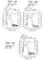
- the annealingis performed in an atmosphere where several percents of vapor is added to hydrogen, as shown in FIG. 2C, it has been found that the boron contained in the silicon is segregated into the metal nitride interface like the annealing in a nitrogen atmosphere.
- phosphorus or arsenic used as an n-type impurity doped in polycrystalline siliconis segregated into the gate insulating film interface composed of silicon oxide on the lower layer and has a high concentration on the interface.
- This phenomenonin which the boron served as a p-type impurity contained in the polycrystalline silicon in the metal nitride film/polycrystalline silicon/gate insulating film structure has a different segregated interface from phosphorus or arsenic served as an n-type impurity contained therein, makes contribution to both simplifying the dual gate CMOS process and reducing leakage of boron at a time.
- boronis contained on the overall surface of the polycrystalline silicon film and a material served as a mask for screening phosphorus or arsenic is coated on the surface outside of the target area.
- an n-type impuritysuch as phosphorus or arsenic is implanted onto the non-mask area by means of the ion-implantation technique or the diffusion technique.
- the mask materialis removed and then another layer such as a metallic nitride layer is formed in place.
- the annealingis performed in a nitrogen atmosphere or a hydrogen atmosphere with vapor added thereto.
- boronis segregated on the metallic nitride interface in the area where boron and an n-type impurity are dually doped (for example, in the case of implanting 2 ⁇ 10 15 /cm 2 of boron or arsenic) and the concentration is made lower to (1 ⁇ 10 20 /cm 2 ) on the insulating film interface on the ground.
- arsenicis segregated onto the gate insulating film interface and thus is high in concentration (2 ⁇ 10 20 /cm 2 ).
- the area in which phosphorus is containedis made to be an n-type one, while the other area includes polycrystalline silicon gate electrode having a p-type conductive characteristic. That is, only one process for specifying a doping area makes it possible to form a dual gate and allow the boron in the polycrystalline silicon to be segregated onto the metallic nitride interface, thereby reducing the leakage of boron.
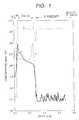
- FIG. 1is a graph showing a measured result by a secondary ion mass spectrograph with respect to the p-type impurity and the n-type impurity in the NMOS of the semiconductor device according to the first embodiment of the invention
- FIGS. 2A to 2 Care graphs showing boron distributions after annealing in the NMOS of the semiconductor according to the invention.
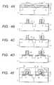
- FIGS. 3A to 3 Eare sectional views of a semiconductor device at each step of a manufacturing method according to the first embodiment of the invention.
- FIGS. 4A to 4 Eare sectional views of a semiconductor device at each step of a manufacturing method according to the first embodiment of the invention.
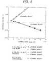
- FIG. 5is a graph showing a comparison between the transistor of the invention and the conventional transistor
- FIGS. 6A to 6 Bare graphs showing dependency of an impurity concentration on a depletion width formed in an n+/p+ junction in the NMOS of the semiconductor device according to the invention and dependency of an impurity concentration on a breakdown voltage of the junction therein;
- FIG. 7is a graph showing a measured result by a secondary ion mass spectrograph with respect to a p-type impurity and an n-type impurity in the NMOS of the semiconductor device according to the third embodiment of the invention.
- the descriptionwill be oriented to a process of making a dual gate CMOS transistor according to this embodiment with reference to FIGS. 3A to 3 E and 4 A to 4 E.
- the descriptionwill be oriented to a stacked gate electrode composed of a metal (tungsten) stacked on the metallic nitride formed on the polycrystalline silicon.
- This structurealso serves to lower the resistance of the gate electrode.
- the left-half portionindicates the NMOS formed area, while the right-half portion indicates the PMOS formed area.
- a p-type 10 ⁇ cm silicon substrate 1is prepared.
- a trench of 400 nmis formed in the interface between elements to be formed on the substrate by means of the photolithography technique and the dry-etching technique.
- a silicon oxide film having a depth of 500 nmis formed by means of the CVD technique.
- the silicon oxide filmis densitied.
- silicon oxideis removed from a flat portion of the silicon substrate by means of the CMP (Chemical Mechanical Polishing) technique and then silicon oxide 2 is buried only in the trench (see FIG. 3 A).
- boronis ion-implanted into the left-half portion and phosphorus is ion-implanted into the right-half portion.
- the annealing of 1000° C. in a nitrogen atmosphereis carried out for 20 minutes.
- an SiO 2 film having a thickness of 2.8 nmis formed.
- the surfaceis heat-treated at an oxide nitrogen atmosphere for forming a silicon oxide nitride film.
- the impurity concentration on the surface of the substrate that is approximate to adjusting the threshold voltage of each MOS transistormay be achieved by ion-implanting phosphorus or boron in the range of 1 ⁇ 10 12 /cm 2 to 3 ⁇ 10 13 /cm 2 .
- various implantationsare tried, even for the dual gate CMOS based on the conventional method, the manufacturing conditions of the MOS transistor having the most approximate threshold voltage are not defined.
- amorphous silicon 6is deposited to a thickness of 70 nm.
- borohydride gasis introduced for doping boron into the amorphous film.
- a certain materialwas produced by using the ion-implanting method for doping boron onto the amorphous silicon film.
- the amorphous silicon film to which no impurity is dopedis pre-formed and then boron ions are implanted at a voltage of 5 keV in the range of 1 ⁇ 10 15 units/cm 2 to 5 ⁇ 10 15 units/cm 2 .
- various materialswere produced with various implantations.
- a silicon oxide filmis deposited at a depth of 200 nm by means of the CVD method. Then, a silicon oxide film 7 is left only at target positions (where the PMOS is formed) on the wafer by means of the photolithography and the dry-etching technique. Afterwards, with this silicon oxide film 7 as a mask, phosphorus 8 is ion-implanted into the amorphous silicon film of a non-masked area (where the NMOS is formed). Various amounts of phosphorus were implanted at 15 keV in the range of 1 ⁇ 10 15 units/cm 2 to 5 ⁇ 10 15 units/cm 2 (see FIG. 3 D).
- tungsten nitride (WNx) 9is formed to have a thickness of 5 nm at a low pressure atmosphere (0.3 Pa) of a mixture of an argon gas and a nitrogen gas by means of the sputtering equipment.
- the tungsten (W)is deposited at a depth of 50 nm by means of the sputtering technique (see FIG. 3 E).
- a silicon nitride film having a depth of 150 nmis formed by means of the plasma CVD method.
- the silicon nitride film 11 located on the top layeris worked to a target gate electrode form (see FIG. 4 A). Then, with the silicon nitride film 11 as the mask, the tungsten, the tungsten nitride and the amorphous silicon layer are worked at a batch (see FIG. 4 B). Afterwards, the photoresist located at the top is removed by the conventional plasma ashing process. Then, the surface oxide of the silicon substrate around the gate electrode that is contaminated and damaged by those dry etching is wet-etched by means of a mixture of hydrofluoric acid and vapor.
- vaporis added to the hydrogen atmosphere at a pressure ratio of 10% and then the annealing is performed at 750° C. and for 30 minutes.
- This heat treatmentresults in oxidizing the silicon substrate surface 12 around the gate electrode and the side wall 13 of the gate electrode silicon layer under W/WNx that has been changed from an amorphous material into a polycrystalline material.
- the annealing at the atmosphere of vapor-added hydrogenresults in selectively oxidizing the exposed silicon surface without oxidizing the tungsten 8 and the tungsten nitride 10 .
- This process for selectively oxidizing the siliconis intended to recovering reliability of the gate oxide film that was subject to damage in the dry-etching process.
- a resist pattern for covering the PMOS areais formed by means of the normal photolithography technique.
- the resist pattern and the silicon nitride film 11 on the NMOS areaas mask materials, by using the ion-implanting device, phosphorus ions of 2 ⁇ 10 13 /cm 2 are implanted onto the silicon substrate at 10 keV for forming an n-type semiconductor area 14 .
- the resist pattern for covering the NMOS areais formed by means of the normal photolithography technique.
- BF 2 ions of 2 ⁇ 10 14 /cm 2are implanted at 10 keV by means of the ion-implanting method, for forming a p-type semiconductor area 15 (see FIG. 4 C).
- the silicon nitride filmis deposited to a thickness of 70 nm by means of the low pressure CVD device. Afterwards, the silicon nitride film on the flat portion is removed by the anisotropic ion etching device, so that the silicon nitride film 16 is left only on the side wall of the gate electrode. Then, in the same procedure of implanting ions, the n-type and p-type impurities are implanted onto the silicon substrate.
- arsenic ions of 2 ⁇ 10 15 /cm 2are implanted as an n-type impurity at 40 keV, and then BF 2 ions of 2 ⁇ 10 15 /cm 2 are implanted as p-type impurity at 15 keV, for forming an n+ type semiconductor area 17 and a p+ type semiconductor area 18 (see FIG. 4 D).
- the annealingis performed for 30 seconds and at a temperature of 950° C. and in a hydrogen atmosphere with 5% of vapor added thereto. This annealing is intended for electrically activating the implanted impurity on the silicon substrate. If this annealing is performed in a nitrogen atmosphere, the hydrogen contained in a silicon nitride film formed on the side wall of the gate electrode causes boron to be likely leaked from the gate electrode into the substrate. After forming the source and the drain of the MOS transistor, the thin silicon oxide film formed on the surface of the silicon substrate is removed by the hydrofluoric acid system etchant.
- Cois deposited to a thickness of 8 nm by means of the sputtering device.
- TiNxOn the layer of Co is deposited TiNx having a depth of 20 nm.
- the annealingis performed at a temperature of 550° C. and in a nitrogen atmosphere.
- the layer of TiN and the layer of Co that is not reactive with the silicon of the substrateare removed by the wet etching method.
- This annealingcauses a CO silicide 19 to be left only on the pre-ion-implanted surface of the silicon substrate for the purpose of self-adjustment.
- the annealing at a temperature of 850° C. and in a nitrogen atmospherecauses the Co silicide to be low in resistance.
- an SiO 2 film served as an interlaminar insulating film 20is deposited at a depth of 500 nm by means of the plasma CVD method. Then, on the surface of the SiO 2 film is coated fused silica glass. Then, the annealing is performed at a temperature of 950° C. and for one minute. Afterwards, a contact hole is formed for electrically conducting a given spot by means of the photolithography and the dry etching technique. In the process for forming the contact hole, the connecting hole to the source and the drain is partially overlapped with the gate electrode in the fine MOS transistor because of the shift of the mask fitting of the photolithography.
- the tungsten layer formed by this sputtering methodis used as a cohesion layer, because the tungsten film formed by the CVD method has poor coherence with the silicon insulating film on the ground.
- this tungsten layeris applied to the interconnection pattern 21 by means of the normal photolithography and the normal dray etching techniques.
- this interconnection layeris deposited a silicon oxide film of 200 nm by means of the plasma CVD method.
- This silicon oxide filmis served as a layer 22 for preventing an intruder that leads to lowering reliability of the semiconductor device such as an contaminant.
- an electrode connecting hole from the outside of the chipis formed at a given area.
- the annealing in a hydrogen atmosphereis performed at a temperature of 450° C. and for 30 minutes. This completes the semiconductor device according to the invention (see FIG. 4 E).
- the estimationis performed with respect to the MOS transistor characteristic of the stacked dual gate CMOS semiconductor device composed of W/WNx/polycrystalline silicon formed by the foregoing processes.
- the two prior artsthat is, the polycrystalline silicon dual gate CMOS semiconductor device formed by the doping separating method with two masks and the stacked dual gate CMOS semiconductor device of W/WNx/polycrystalline silicon doped by the same method, were prepared.
- the formation of the dual gate by the conventional methodneeds a process of forming a mask for selecting an ion-implanting area for doping an impurity to a amorphous silicon layer twice.
- These processesare a mask forming process for doping an n-type or p-type impurity into a specific area after forming the amorphous silicon and another mask forming process for doping an opposite type impurity on the remaining amorphous silicon area as covering the pre-doped area with a mask material.
- the formation of the mask materials on the specific areaneeds the photolithography and the dry etching processes and the accessory process for removing the mask materials.
- the estimationis performed with respect to the transistor characteristic of the present embodiment and the dual gate CMOS semiconductor device created for the comparison.
- the dependency on the impurity concentrationwas obtained.
- the impurity introduced into the channel areais intended for adjusting the threshold voltage of the n-channel and the p-channel MOS transistors whose gate electrode working dimension is 0.25 ⁇ m.
- the threshold voltage of the MOS transistor formed by this embodimentindicates the almost same dependency on the impurity concentration of the channel area as the characteristic of the stacked dual gate CMOS semiconductor device formed by the conventional method.
- these threshold voltagesare in proportion to the concentration of the impurity contained in the channel area. Hence, the leakage of boron to the substrate is negligible in the operation of the circuit.
- the threshold voltage on the substrate surface of the p-channel MOS transistoris shifted from an estimated value by 0.5 V to 1.0 V.
- boronis so much leaked that the n-type substrate surface may be changed into the p-type one.
- no normal MOS transistor characteristiccould be obtained.
- the n-channel MOS transistorindicates the estimated dependency on the concentration of the channel area in the substrate even if it uses any type of gate electrode. It is understood from these results that the dual gate CMOS formed by the present invention allows the n-channel and the p-channel MOS transistors to operate normally.
- the other transistor basic characteristicssuch as channel conductance and driving current do not indicate any defect in an element characteristic caused by dually doping the n-type and p-type impurities onto the amorphous silicon layer.
- the dual gate CMOSdoes not show any defective transistor characteristic.
- the n-type and the p-type junctionsare formed in the thickness direction of the polycrystalline silicon layer of the stacked gate electrode as shown in FIG. 1 .
- the depletion layeris formed on the interface between the junctions, so that it may disadvantageously serve to be non-conductive. Then, the relationship between the depletion width and the applied voltage/concentration of the substrate and the relationship between the breakdown voltage of the pn junction and the concentration of the substrate were obtained by calculation. As shown in FIGS.
- the concentration of the impurityis about 5 ⁇ 10 18 /cm 3 or more
- the depletion widthis 1 nm or lower and the breakdown voltage of the junction is 0.1 V or lower as well.
- the junctionindicates the stepwise distribution of the impurity.
- both of the n-type and the p-type impuritiesreach as high a concentration as 1 ⁇ 10 20 /cm 3 or more. It means that no defective conduction caused by the formation of the depletion layer is brought about.
- the signal delay time of the device formed according to the inventionindicates the same value as the prior art in which the impurities are separately doped into the polycrystalline silicon.
- the signal delay time per one stepwas 20 picoseconds.
- the estimationis performed with respect to the foreign particle appearing in the doping-related process in the present invention and the semiconductor device in which the conventional impurity doping method is applied to the polycrystalline silicon layer.
- the conventional method100 to 200 foreign particles, each of which is 0.3 ⁇ m or more, were detected per an 8-inch wafer, while for the present invention, 10 to 80 foreign particles were detected. This is because the number of steps for doping the impurities is reduced from 16 to 8.
- the foreign particleswere reduced more than those caused by doping boron with the ion-implantation method after forming the film, concretely, the number of those foreign particles were reduced to 10 to 40.
- the reduction of the foreign particles and the manufacturing steps in this embodimentserves to improve the manufacturing yield of the semiconductor device more than the conventional method by about 5%.
- the reduction of the manufacturing steps and the improvement of the yieldmay lead to reduction of the manufacturing cost by several percents though it does not apply to any type of semiconductor device. It is assured that the boron segregation onto the WNx interface by the annealing in the hydrogen atmosphere with vapor added thereto leads to suppressing the shift of the threshold voltage of the MOS transistor caused by the boron leakage rather than the conventional polycrystalline silicon gate.
- the hydrogen contained in the silicon nitride film for gate working mask and the gate side all silicon nitride film for LDDcauses the p+ polycrystalline silicon gate MOS transistor to invert the type of the channel area substrate surface into the p type, thereby being unable to indicate the normal transistor characteristic.
- the present inventionmakes contribution to suppressing the fluctuation into 50 mV to 300 mV rather than the case where no boron is leaked. It is considered that this sort of fluctuation does not have an adverse effect on the circuit performance if a device and a circuit design are a little devised.
- the dual gate CMOS semiconductor devicewas manufactured in the almost same process as the first embodiment. In this embodiment, however, the doping of impurity into the amorphous silicon was performed in the following procedure, which is the same as that of the first embodiment except the doping process.
- the amorphous'silicon 6was deposited.
- the phosphorus ionswere implanted on the portion where no mask material 7 is covered at 10 keV and in the range of 1 ⁇ 10 14 /cm 2 and 1 ⁇ 10 15 /cm 2 to 5 ⁇ 10 15 /cm 2 or more.
- boronwas implanted on the overall surface of the wafer at 3 keV and in the range of 2 ⁇ 10 18 /cm 3 for doping the boron.
- the boron doping methodin addition to the ion implanting method, another method was studied such as an annealing in the state of flowing gas containing boron hydrocarbon and a solid source method for heating boron nitride for doping boron.
- phosphoruswas doped only at the location where the gate of the n-channel MOS transistor is to be formed. Then, boron was doped. It is found that the doped phosphorus is effective in suppressing leakage of the boron doped later onto the substrate through the annealing.
- the annealing in the hydrogen atmosphere containing vaporis performed for suppressing leakage of boron.
- the annealing in the hydrogen atmosphere with no vaporserves to suppress leakage of boron resulting from the phosphorus. That is, the p-channel MOS transistor composed of amorphous silicon with no phosphorus causes the type of the channel area to be inverted into the p-type because of too much leaked boron, thereby being unable to operate properly. On the other hand, the n-channel MOS transistor composed of amorphous silicon with phosphorus doped therein has few leaked boron.
- the shift of its threshold voltage against the threshold voltage of the transistor with no boron leakedis so small as 0.1 to 0.7 V. It means that the n-channel MOS transistor indicates the normal MOS transistor characteristic. This embodiment, therefore, enables to expand the thermal budget against the leaked boron further than the first embodiment.
- the concentration of phosphorus segregated at the gate dielectric film interfaceis about 5 ⁇ 10 19 /cm 2 .
- the n-type impurity concentration on the interface with the gate insulating filmis smaller than the p-type impurity, so that the depletion layer may be formed in the silicon layer of the gate electrode in some applied voltages.
- the concentration of phosphorusis 1 ⁇ 10 15 /cm 2 or more, the normal n-channel MOS transistor characteristic was obtained.
- arsenic ions of 2 ⁇ 10 15 /cm 2were implanted at such an energy as a projection range into the middle of the amorphous or polycrystalline silicon layer.
- the distribution of the impurity in the depth direction of the silicon layer of the n-channel gate electrode of the stacked dual gate CMOS semiconductor device manufactured as aboveis illustrated in FIG. 7 . It is obvious from FIG. 7 that the n-type impurity concentration at the n+/p+ junction formed within the polycrystalline silicon layer has a higher concentration than those of the first and the second embodiments. Hence, the resistance at the junction may be reduced further.
- antimonymay be used for offering the same effect.
- n-type impurity to be dopedin place of phosphorus, arsenic or antimony may be used for achieving the object of the invention.
- the annealing of 700° C. or moreis required for segregating these impurities on the interface of the gate insulating film.
- the boron ionsare used for doping boron by means of the ion implanting method.
- the compound ionssuch as boron fluoride may be used for doping boron.
- the semiconductor devices of these embodimentsenable to reduce the number of the manufacturing steps, which leads to reduction of the manufacturing period, improvement of the yield, and reduction of the manufacturing cost of the semiconductor device.
- the present inventionis characterized by the stacked gate electrode structure and the segregation of boron on the metal nitride interface. This segregation effect serves to reduce the leaked boron.
Landscapes
- Metal-Oxide And Bipolar Metal-Oxide Semiconductor Integrated Circuits (AREA)
- Electrodes Of Semiconductors (AREA)
Abstract
Description
Claims (20)
Priority Applications (4)
| Application Number | Priority Date | Filing Date | Title |
|---|---|---|---|
| US10/272,369US6645799B2 (en) | 2000-01-24 | 2002-10-17 | Method of manufacturing a dual gate semiconductor device with a poly-metal electrode |
| US10/448,351US6727132B2 (en) | 2000-01-24 | 2003-05-30 | Method of manufacturing a dual gate semiconductor device with a poly-metal electrode |
| US10/787,436US6881618B2 (en) | 2000-01-24 | 2004-02-27 | Method of manufacturing a dual gate semiconductor device with a poly-metal electrode |
| US10/787,437US7049665B2 (en) | 2000-01-24 | 2004-02-27 | Method of manufacturing a dual gate semiconductor device with a poly-metal electrode |
Applications Claiming Priority (2)
| Application Number | Priority Date | Filing Date | Title |
|---|---|---|---|
| JP2000-017875 | 2000-01-24 | ||
| JP2000017875AJP2001210726A (en) | 2000-01-24 | 2000-01-24 | Semiconductor device and manufacturing method thereof |
Related Child Applications (1)
| Application Number | Title | Priority Date | Filing Date |
|---|---|---|---|
| US10/272,369DivisionUS6645799B2 (en) | 2000-01-24 | 2002-10-17 | Method of manufacturing a dual gate semiconductor device with a poly-metal electrode |
Publications (1)
| Publication Number | Publication Date |
|---|---|
| US6503788B1true US6503788B1 (en) | 2003-01-07 |
Family
ID=18544804
Family Applications (5)
| Application Number | Title | Priority Date | Filing Date |
|---|---|---|---|
| US09/639,306Expired - LifetimeUS6503788B1 (en) | 2000-01-24 | 2000-08-16 | Semiconductor device and method of manufacture thereof |
| US10/272,369Expired - Fee RelatedUS6645799B2 (en) | 2000-01-24 | 2002-10-17 | Method of manufacturing a dual gate semiconductor device with a poly-metal electrode |
| US10/448,351Expired - Fee RelatedUS6727132B2 (en) | 2000-01-24 | 2003-05-30 | Method of manufacturing a dual gate semiconductor device with a poly-metal electrode |
| US10/787,436Expired - Fee RelatedUS6881618B2 (en) | 2000-01-24 | 2004-02-27 | Method of manufacturing a dual gate semiconductor device with a poly-metal electrode |
| US10/787,437Expired - LifetimeUS7049665B2 (en) | 2000-01-24 | 2004-02-27 | Method of manufacturing a dual gate semiconductor device with a poly-metal electrode |
Family Applications After (4)
| Application Number | Title | Priority Date | Filing Date |
|---|---|---|---|
| US10/272,369Expired - Fee RelatedUS6645799B2 (en) | 2000-01-24 | 2002-10-17 | Method of manufacturing a dual gate semiconductor device with a poly-metal electrode |
| US10/448,351Expired - Fee RelatedUS6727132B2 (en) | 2000-01-24 | 2003-05-30 | Method of manufacturing a dual gate semiconductor device with a poly-metal electrode |
| US10/787,436Expired - Fee RelatedUS6881618B2 (en) | 2000-01-24 | 2004-02-27 | Method of manufacturing a dual gate semiconductor device with a poly-metal electrode |
| US10/787,437Expired - LifetimeUS7049665B2 (en) | 2000-01-24 | 2004-02-27 | Method of manufacturing a dual gate semiconductor device with a poly-metal electrode |
Country Status (4)
| Country | Link |
|---|---|
| US (5) | US6503788B1 (en) |
| JP (1) | JP2001210726A (en) |
| KR (1) | KR100767917B1 (en) |
| TW (1) | TW517379B (en) |
Cited By (15)
| Publication number | Priority date | Publication date | Assignee | Title |
|---|---|---|---|---|
| US20030122199A1 (en)* | 2001-12-18 | 2003-07-03 | Kabushiki Kaisha Toshiba | Semiconductor device and fabricating method for the same |
| US20030179793A1 (en)* | 2002-03-19 | 2003-09-25 | Nippon Telegraph And Telephone Corporation | Thin film deposition method of nitride semiconductor and nitride semiconductor light emitting device |
| US20030207588A1 (en)* | 2001-01-26 | 2003-11-06 | Matthias Goldbach | Semiconductor configuration and process for etching a layer of the semiconductor configuration using a silicon-containing etching mask |
| US20030216038A1 (en)* | 2002-05-20 | 2003-11-20 | Sucharita Madhukar | Dual metal gate transistors for CMOS process |
| US20040033678A1 (en)* | 2002-08-14 | 2004-02-19 | Reza Arghavani | Method and apparatus to prevent lateral oxidation in a transistor utilizing an ultra thin oxygen-diffusion barrier |
| US6727132B2 (en) | 2000-01-24 | 2004-04-27 | Renesas Technology Corp. | Method of manufacturing a dual gate semiconductor device with a poly-metal electrode |
| US6763164B2 (en)* | 2000-03-13 | 2004-07-13 | The Furukawa Electric Co., Ltd. | Method for manufacturing a planar lightwave circuit, and planar waveguide circuit |
| US20040150108A1 (en)* | 2002-11-29 | 2004-08-05 | Axel Buerke | Low resistance barrier for a microelectronic component and method for fabricating the same |
| US20050062115A1 (en)* | 1999-12-28 | 2005-03-24 | Fujitsu Limited | Semiconductor device having gate electrodes with polymetal structure of polycrystalline silicon films and metal films |
| US20050112814A1 (en)* | 2003-11-21 | 2005-05-26 | Eun-Kuk Chung | Method of fabricating CMOS transistor that prevents gate thinning |
| US20060024932A1 (en)* | 2004-08-02 | 2006-02-02 | Heung-Sik Park | Methods of forming semiconductor devices including removing a thickness of a polysilicon gate layer |
| US7018887B1 (en)* | 2004-03-01 | 2006-03-28 | Advanced Micro Devices, Inc. | Dual metal CMOS transistors with silicon-metal-silicon stacked gate electrode |
| US20080199994A1 (en)* | 2003-03-26 | 2008-08-21 | Yuko Ohgishi | Method of Producing Semiconductor Device and Semiconductor Device |
| US20090096034A1 (en)* | 2007-10-16 | 2009-04-16 | International Business Machines Corporation | Partially and Fully Silicided Gate Stacks |
| US20090166629A1 (en)* | 2007-12-31 | 2009-07-02 | Texas Instruments Incorporated | Reducing gate cd bias in cmos processing |
Families Citing this family (18)
| Publication number | Priority date | Publication date | Assignee | Title |
|---|---|---|---|---|
| KR100568859B1 (en)* | 2003-08-21 | 2006-04-10 | 삼성전자주식회사 | Method for manufacturing transistor of DRAM semiconductor device |
| KR100843223B1 (en)* | 2007-01-03 | 2008-07-02 | 삼성전자주식회사 | Semiconductor device adopting heterogeneous metal gate structure according to channel type and its manufacturing method |
| KR100586737B1 (en)* | 2003-12-26 | 2006-06-08 | 한국전자통신연구원 | NMOS devices, PMOS devices and SiSiWOCMOS devices implemented on a SOI substrate, and methods of manufacturing the same |
| KR100623251B1 (en)* | 2004-02-19 | 2006-09-18 | 삼성에스디아이 주식회사 | Method for manufacturing polycrystalline silicon thin film and thin film transistor using polycrystalline silicon manufactured using same |
| JP2005317736A (en)* | 2004-04-28 | 2005-11-10 | Elpida Memory Inc | Manufacturing method of semiconductor device |
| JP4054321B2 (en)* | 2004-06-23 | 2008-02-27 | 松下電器産業株式会社 | Semiconductor device |
| KR100666552B1 (en)* | 2004-06-30 | 2007-01-09 | 삼성에스디아이 주식회사 | Manufacturing method of semiconductor device and semiconductor device manufactured by this method |
| KR100666563B1 (en)* | 2004-07-05 | 2007-01-09 | 삼성에스디아이 주식회사 | Method for manufacturing semiconductor device and semiconductor device manufactured by this method |
| US7355228B2 (en)* | 2004-10-15 | 2008-04-08 | Omnivision Technologies, Inc. | Image sensor pixel having photodiode with multi-dopant implantation |
| JP4782411B2 (en) | 2004-12-16 | 2011-09-28 | エルピーダメモリ株式会社 | Semiconductor device and manufacturing method thereof |
| KR100596803B1 (en) | 2005-06-30 | 2006-07-04 | 주식회사 하이닉스반도체 | Method of manufacturing semiconductor device |
| KR100688555B1 (en)* | 2005-06-30 | 2007-03-02 | 삼성전자주식회사 | A semiconductor device comprising a MOS transistor and a manufacturing method therefor |
| US7378713B2 (en)* | 2006-10-25 | 2008-05-27 | Taiwan Semiconductor Manufacturing Co., Ltd. | Semiconductor devices with dual-metal gate structures and fabrication methods thereof |
| US7812414B2 (en)* | 2007-01-23 | 2010-10-12 | Taiwan Semiconductor Manufacturing Company, Ltd. | Hybrid process for forming metal gates |
| US8536660B2 (en)* | 2008-03-12 | 2013-09-17 | Taiwan Semiconductor Manufacturing Company, Ltd. | Hybrid process for forming metal gates of MOS devices |
| US8013400B1 (en)* | 2008-04-21 | 2011-09-06 | National Semiconductor Corporation | Method and system for scaling channel length |
| DK2555789T3 (en)* | 2010-04-08 | 2020-07-20 | Inst Nat Sante Rech Med | INHIBITANT PEPTIDES DERIVED FROM TREM-LIKE TRANSCRIPT 1 (TLT-1) AND USES THEREOF |
| KR101830170B1 (en)* | 2011-05-17 | 2018-02-21 | 삼성디스플레이 주식회사 | Oxide semiconductor device, method of forming an oxide semiconductor device, and display device having an oxide semiconductor device, method of manufacturing a display device having an oxide semiconductor device |
Citations (3)
| Publication number | Priority date | Publication date | Assignee | Title |
|---|---|---|---|---|
| US5683920A (en)* | 1995-12-29 | 1997-11-04 | Hyundai Electronics Industries Co., Ltd. | Method for fabricating semiconductor devices |
| US5780330A (en)* | 1996-06-28 | 1998-07-14 | Integrated Device Technology, Inc. | Selective diffusion process for forming both n-type and p-type gates with a single masking step |
| US6300184B1 (en)* | 1999-06-30 | 2001-10-09 | Hyundai Electronics Industries Co., Ltd. | Method of manufacturing a CMOS transistor |
Family Cites Families (23)
| Publication number | Priority date | Publication date | Assignee | Title |
|---|---|---|---|---|
| US4420344A (en)* | 1981-10-15 | 1983-12-13 | Texas Instruments Incorporated | CMOS Source/drain implant process without compensation of polysilicon doping |
| IT1223571B (en)* | 1987-12-21 | 1990-09-19 | Sgs Thomson Microelectronics | PROCEDURE FOR THE MANUFACTURE OF INTEGRATED CMOS DEVICES WITH REDUCED DOOR LENGTHS |
| KR930010124B1 (en)* | 1991-02-27 | 1993-10-14 | 삼성전자 주식회사 | Manufacturing Method and Structure of Semiconductor Transistor |
| US5278085A (en)* | 1992-08-11 | 1994-01-11 | Micron Semiconductor, Inc. | Single mask process for forming both n-type and p-type gates in a polycrystalline silicon layer during the formation of a semiconductor device |
| US5656519A (en)* | 1995-02-14 | 1997-08-12 | Nec Corporation | Method for manufacturing salicide semiconductor device |
| US5674788A (en)* | 1995-06-06 | 1997-10-07 | Advanced Micro Devices, Inc. | Method of forming high pressure silicon oxynitride gate dielectrics |
| DE19525069C1 (en)* | 1995-07-10 | 1996-10-24 | Siemens Ag | Dual work function gate-type CMOS circuit prodn. |
| KR0167273B1 (en)* | 1995-12-02 | 1998-12-15 | 문정환 | High voltage mosfet device and manufacturing method thereof |
| KR970053916A (en)* | 1995-12-27 | 1997-07-31 | 김주용 | Manufacturing method of semiconductor device |
| US6051459A (en)* | 1997-02-21 | 2000-04-18 | Advanced Micro Devices, Inc. | Method of making N-channel and P-channel IGFETs using selective doping and activation for the N-channel gate |
| US5888588A (en)* | 1997-03-31 | 1999-03-30 | Motorola, Inc. | Process for forming a semiconductor device |
| KR100249798B1 (en)* | 1997-12-19 | 2000-03-15 | 정선종 | Formation of thin junction layer and ion gate mask semiconductor device using ion implantation mask layer |
| US6087225A (en)* | 1998-02-05 | 2000-07-11 | International Business Machines Corporation | Method for dual gate oxide dual workfunction CMOS |
| US5963799A (en)* | 1998-03-23 | 1999-10-05 | Texas Instruments - Acer Incorporated | Blanket well counter doping process for high speed/low power MOSFETs |
| JP3515363B2 (en)* | 1998-03-24 | 2004-04-05 | 株式会社東芝 | Method for manufacturing semiconductor device |
| US6051458A (en)* | 1998-05-04 | 2000-04-18 | Taiwan Semiconductor Manufacturing Company | Drain and source engineering for ESD-protection transistors |
| US5942781A (en)* | 1998-06-08 | 1999-08-24 | Sun Microsystems, Inc. | Tunable threshold SOI device using back gate well |
| US5960289A (en)* | 1998-06-22 | 1999-09-28 | Motorola, Inc. | Method for making a dual-thickness gate oxide layer using a nitride/oxide composite region |
| US6157204A (en)* | 1998-08-05 | 2000-12-05 | Micron Technology, Inc. | Buffer with adjustable slew rate and a method of providing an adjustable slew rate |
| US6399432B1 (en)* | 1998-11-24 | 2002-06-04 | Philips Semiconductors Inc. | Process to control poly silicon profiles in a dual doped poly silicon process |
| KR100631011B1 (en)* | 1999-08-12 | 2006-10-04 | 엘지.필립스 엘시디 주식회사 | Method of manufacturing thin film transistor |
| JP2001203347A (en)* | 2000-01-18 | 2001-07-27 | Mitsubishi Electric Corp | Semiconductor device and method of manufacturing the same |
| JP2001210726A (en) | 2000-01-24 | 2001-08-03 | Hitachi Ltd | Semiconductor device and manufacturing method thereof |
- 2000
- 2000-01-24JPJP2000017875Apatent/JP2001210726A/enactivePending
- 2000-07-26TWTW089114963Apatent/TW517379B/ennot_activeIP Right Cessation
- 2000-08-16USUS09/639,306patent/US6503788B1/ennot_activeExpired - Lifetime
- 2000-08-17KRKR1020000047475Apatent/KR100767917B1/ennot_activeExpired - Fee Related
- 2002
- 2002-10-17USUS10/272,369patent/US6645799B2/ennot_activeExpired - Fee Related
- 2003
- 2003-05-30USUS10/448,351patent/US6727132B2/ennot_activeExpired - Fee Related
- 2004
- 2004-02-27USUS10/787,436patent/US6881618B2/ennot_activeExpired - Fee Related
- 2004-02-27USUS10/787,437patent/US7049665B2/ennot_activeExpired - Lifetime
Patent Citations (3)
| Publication number | Priority date | Publication date | Assignee | Title |
|---|---|---|---|---|
| US5683920A (en)* | 1995-12-29 | 1997-11-04 | Hyundai Electronics Industries Co., Ltd. | Method for fabricating semiconductor devices |
| US5780330A (en)* | 1996-06-28 | 1998-07-14 | Integrated Device Technology, Inc. | Selective diffusion process for forming both n-type and p-type gates with a single masking step |
| US6300184B1 (en)* | 1999-06-30 | 2001-10-09 | Hyundai Electronics Industries Co., Ltd. | Method of manufacturing a CMOS transistor |
Non-Patent Citations (1)
| Title |
|---|
| IEEE Electron device Let., vol. 17, No. 11, Nov., 1996, pp. 497-499. |
Cited By (30)
| Publication number | Priority date | Publication date | Assignee | Title |
|---|---|---|---|---|
| US20050062115A1 (en)* | 1999-12-28 | 2005-03-24 | Fujitsu Limited | Semiconductor device having gate electrodes with polymetal structure of polycrystalline silicon films and metal films |
| US6939787B2 (en)* | 1999-12-28 | 2005-09-06 | Fujitsu Limited | Method for fabricating semiconductor device having gate electrode with polymetal structure of polycrystalline silicon film and metal film |
| US6881618B2 (en) | 2000-01-24 | 2005-04-19 | Renesas Technology Corp. | Method of manufacturing a dual gate semiconductor device with a poly-metal electrode |
| US20040180490A1 (en)* | 2000-01-24 | 2004-09-16 | Naoki Yamamoto | Method of manufacturing a dual gate semiconductor device with a poly-metal electrode |
| US7049665B2 (en) | 2000-01-24 | 2006-05-23 | Hitachi, Ltd. | Method of manufacturing a dual gate semiconductor device with a poly-metal electrode |
| US6727132B2 (en) | 2000-01-24 | 2004-04-27 | Renesas Technology Corp. | Method of manufacturing a dual gate semiconductor device with a poly-metal electrode |
| US6763164B2 (en)* | 2000-03-13 | 2004-07-13 | The Furukawa Electric Co., Ltd. | Method for manufacturing a planar lightwave circuit, and planar waveguide circuit |
| US6864188B2 (en)* | 2001-01-26 | 2005-03-08 | Infineon Technologies Ag | Semiconductor configuration and process for etching a layer of the semiconductor configuration using a silicon-containing etching mask |
| US20030207588A1 (en)* | 2001-01-26 | 2003-11-06 | Matthias Goldbach | Semiconductor configuration and process for etching a layer of the semiconductor configuration using a silicon-containing etching mask |
| US20030122199A1 (en)* | 2001-12-18 | 2003-07-03 | Kabushiki Kaisha Toshiba | Semiconductor device and fabricating method for the same |
| US7122470B2 (en) | 2001-12-18 | 2006-10-17 | Kabushiki Kaisha Toshiba | Semiconductor device with a CMOS transistor |
| US20060138554A1 (en)* | 2001-12-18 | 2006-06-29 | Kabushiki Kaisha Toshiba | Semiconductor device and fabricating method for the same |
| US6920166B2 (en)* | 2002-03-19 | 2005-07-19 | Nippon Telegraph & Telephone Corporation | Thin film deposition method of nitride semiconductor and nitride semiconductor light emitting device |
| US20030179793A1 (en)* | 2002-03-19 | 2003-09-25 | Nippon Telegraph And Telephone Corporation | Thin film deposition method of nitride semiconductor and nitride semiconductor light emitting device |
| US20030216038A1 (en)* | 2002-05-20 | 2003-11-20 | Sucharita Madhukar | Dual metal gate transistors for CMOS process |
| US6794281B2 (en)* | 2002-05-20 | 2004-09-21 | Freescale Semiconductor, Inc. | Dual metal gate transistors for CMOS process |
| US20040033678A1 (en)* | 2002-08-14 | 2004-02-19 | Reza Arghavani | Method and apparatus to prevent lateral oxidation in a transistor utilizing an ultra thin oxygen-diffusion barrier |
| US20040150108A1 (en)* | 2002-11-29 | 2004-08-05 | Axel Buerke | Low resistance barrier for a microelectronic component and method for fabricating the same |
| US20080199994A1 (en)* | 2003-03-26 | 2008-08-21 | Yuko Ohgishi | Method of Producing Semiconductor Device and Semiconductor Device |
| US7943446B2 (en)* | 2003-03-26 | 2011-05-17 | Sony Corporation | Method of producing semiconductor device and semiconductor device |
| US20050112814A1 (en)* | 2003-11-21 | 2005-05-26 | Eun-Kuk Chung | Method of fabricating CMOS transistor that prevents gate thinning |
| US7268029B2 (en)* | 2003-11-21 | 2007-09-11 | Samsung Electronics Co., Ltd. | Method of fabricating CMOS transistor that prevents gate thinning |
| US7018887B1 (en)* | 2004-03-01 | 2006-03-28 | Advanced Micro Devices, Inc. | Dual metal CMOS transistors with silicon-metal-silicon stacked gate electrode |
| US20060024932A1 (en)* | 2004-08-02 | 2006-02-02 | Heung-Sik Park | Methods of forming semiconductor devices including removing a thickness of a polysilicon gate layer |
| US20090096034A1 (en)* | 2007-10-16 | 2009-04-16 | International Business Machines Corporation | Partially and Fully Silicided Gate Stacks |
| US7785952B2 (en)* | 2007-10-16 | 2010-08-31 | International Business Machines Corporation | Partially and fully silicided gate stacks |
| US20100224940A1 (en)* | 2007-10-16 | 2010-09-09 | International Business Machines Corporation | Partially and Fully Silicided Gate Stacks |
| US7960795B2 (en) | 2007-10-16 | 2011-06-14 | International Business Machines Corporation | Partially and fully silicided gate stacks |
| US20090166629A1 (en)* | 2007-12-31 | 2009-07-02 | Texas Instruments Incorporated | Reducing gate cd bias in cmos processing |
| US7910422B2 (en)* | 2007-12-31 | 2011-03-22 | Texas Instruments Incorporated | Reducing gate CD bias in CMOS processing |
Also Published As
| Publication number | Publication date |
|---|---|
| US7049665B2 (en) | 2006-05-23 |
| KR100767917B1 (en) | 2007-10-17 |
| US20040164358A1 (en) | 2004-08-26 |
| US6727132B2 (en) | 2004-04-27 |
| US6881618B2 (en) | 2005-04-19 |
| US20030057499A1 (en) | 2003-03-27 |
| US20040180490A1 (en) | 2004-09-16 |
| KR20010076173A (en) | 2001-08-11 |
| US20030203611A1 (en) | 2003-10-30 |
| US6645799B2 (en) | 2003-11-11 |
| TW517379B (en) | 2003-01-11 |
| JP2001210726A (en) | 2001-08-03 |
Similar Documents
| Publication | Publication Date | Title |
|---|---|---|
| US6503788B1 (en) | Semiconductor device and method of manufacture thereof | |
| US5723893A (en) | Method for fabricating double silicide gate electrode structures on CMOS-field effect transistors | |
| CN101300677B (en) | Electrically programmable fuse and method of making same | |
| US7687869B2 (en) | Semiconductor device and method of manufacturing the same | |
| US6436783B1 (en) | Method of forming MOS transistor | |
| EP0700093A1 (en) | Semiconductor device and method of manufacturing the same | |
| US4663825A (en) | Method of manufacturing semiconductor device | |
| US20070298598A1 (en) | Semiconductor device and method of fabricating semiconductor device | |
| JP2001156290A (en) | Semiconductor device | |
| US5723356A (en) | Fabrication method for semiconductor device | |
| WO2000055897A1 (en) | Method of manufacturing a mis field-effect transistor | |
| US5885874A (en) | Method of making enhancement-mode and depletion-mode IGFETS using selective doping of a gate material | |
| US4517731A (en) | Double polysilicon process for fabricating CMOS integrated circuits | |
| US6586333B1 (en) | Integrated plasma treatment and nickel deposition and tool for performing same | |
| US5081518A (en) | Use of a polysilicon layer for local interconnect in a CMOS or BICMOS technology incorporating sidewall spacers | |
| US9953831B1 (en) | Device structures with multiple nitrided layers | |
| KR100201246B1 (en) | Semiconductor device and method of fabricating the same | |
| US6780700B2 (en) | Method of fabricating deep sub-micron CMOS source/drain with MDD and selective CVD silicide | |
| JPH0917867A (en) | Method for forming contact portion in semiconductor device | |
| JP3293987B2 (en) | Method for manufacturing semiconductor device | |
| JPH11340424A (en) | Manufacture of semiconductor device | |
| JP2968548B2 (en) | Semiconductor device and manufacturing method thereof | |
| US5290713A (en) | Process of manufacturing a semiconductor device by using a photoresist mask which does not encircle an area of implanted ions | |
| JP3419956B2 (en) | Method for manufacturing semiconductor device | |
| KR950001171B1 (en) | Semiconductor device and manufacturing method thereof |
Legal Events
| Date | Code | Title | Description |
|---|---|---|---|
| AS | Assignment | Owner name:HITACHI, LTD., JAPAN Free format text:ASSIGNMENT OF ASSIGNORS INTEREST;ASSIGNOR:YAMAMOTO, NAOKI;REEL/FRAME:011016/0328 Effective date:20000718 | |
| STCF | Information on status: patent grant | Free format text:PATENTED CASE | |
| FEPP | Fee payment procedure | Free format text:PAYOR NUMBER ASSIGNED (ORIGINAL EVENT CODE: ASPN); ENTITY STATUS OF PATENT OWNER: LARGE ENTITY | |
| FEPP | Fee payment procedure | Free format text:PAYOR NUMBER ASSIGNED (ORIGINAL EVENT CODE: ASPN); ENTITY STATUS OF PATENT OWNER: LARGE ENTITY | |
| FPAY | Fee payment | Year of fee payment:4 | |
| REMI | Maintenance fee reminder mailed | ||
| FPAY | Fee payment | Year of fee payment:8 | |
| SULP | Surcharge for late payment | Year of fee payment:7 | |
| AS | Assignment | Owner name:RENESAS ELECTRONICS CORPORATION, JAPAN Free format text:ASSIGNMENT OF ASSIGNORS INTEREST;ASSIGNOR:HITACHI, LTD.;REEL/FRAME:026109/0528 Effective date:20110307 | |
| AS | Assignment | Owner name:TESSERA ADVANCED TECHNOLOGIES, INC., CALIFORNIA Free format text:ASSIGNMENT OF ASSIGNORS INTEREST;ASSIGNOR:RENESAS ELECTRONICS CORPORATION;REEL/FRAME:032892/0212 Effective date:20140318 | |
| FPAY | Fee payment | Year of fee payment:12 | |
| SULP | Surcharge for late payment | Year of fee payment:11 | |
| AS | Assignment | Owner name:ROYAL BANK OF CANADA, AS COLLATERAL AGENT, CANADA Free format text:SECURITY INTEREST;ASSIGNORS:INVENSAS CORPORATION;TESSERA, INC.;TESSERA ADVANCED TECHNOLOGIES, INC.;AND OTHERS;REEL/FRAME:040797/0001 Effective date:20161201 | |
| AS | Assignment | Owner name:BANK OF AMERICA, N.A., NORTH CAROLINA Free format text:SECURITY INTEREST;ASSIGNORS:ROVI SOLUTIONS CORPORATION;ROVI TECHNOLOGIES CORPORATION;ROVI GUIDES, INC.;AND OTHERS;REEL/FRAME:053468/0001 Effective date:20200601 | |
| AS | Assignment | Owner name:IBIQUITY DIGITAL CORPORATION, MARYLAND Free format text:RELEASE BY SECURED PARTY;ASSIGNOR:ROYAL BANK OF CANADA;REEL/FRAME:052920/0001 Effective date:20200601 Owner name:FOTONATION CORPORATION (F/K/A DIGITALOPTICS CORPORATION AND F/K/A DIGITALOPTICS CORPORATION MEMS), CALIFORNIA Free format text:RELEASE BY SECURED PARTY;ASSIGNOR:ROYAL BANK OF CANADA;REEL/FRAME:052920/0001 Effective date:20200601 Owner name:INVENSAS CORPORATION, CALIFORNIA Free format text:RELEASE BY SECURED PARTY;ASSIGNOR:ROYAL BANK OF CANADA;REEL/FRAME:052920/0001 Effective date:20200601 Owner name:INVENSAS BONDING TECHNOLOGIES, INC. (F/K/A ZIPTRONIX, INC.), CALIFORNIA Free format text:RELEASE BY SECURED PARTY;ASSIGNOR:ROYAL BANK OF CANADA;REEL/FRAME:052920/0001 Effective date:20200601 Owner name:DTS LLC, CALIFORNIA Free format text:RELEASE BY SECURED PARTY;ASSIGNOR:ROYAL BANK OF CANADA;REEL/FRAME:052920/0001 Effective date:20200601 Owner name:PHORUS, INC., CALIFORNIA Free format text:RELEASE BY SECURED PARTY;ASSIGNOR:ROYAL BANK OF CANADA;REEL/FRAME:052920/0001 Effective date:20200601 Owner name:TESSERA, INC., CALIFORNIA Free format text:RELEASE BY SECURED PARTY;ASSIGNOR:ROYAL BANK OF CANADA;REEL/FRAME:052920/0001 Effective date:20200601 Owner name:TESSERA ADVANCED TECHNOLOGIES, INC, CALIFORNIA Free format text:RELEASE BY SECURED PARTY;ASSIGNOR:ROYAL BANK OF CANADA;REEL/FRAME:052920/0001 Effective date:20200601 Owner name:DTS, INC., CALIFORNIA Free format text:RELEASE BY SECURED PARTY;ASSIGNOR:ROYAL BANK OF CANADA;REEL/FRAME:052920/0001 Effective date:20200601 |