US6501331B2 - Multi-band amplifier - Google Patents
Multi-band amplifierDownload PDFInfo
- Publication number
- US6501331B2 US6501331B2US09/821,177US82117701AUS6501331B2US 6501331 B2US6501331 B2US 6501331B2US 82117701 AUS82117701 AUS 82117701AUS 6501331 B2US6501331 B2US 6501331B2
- Authority
- US
- United States
- Prior art keywords
- amplifier
- impedance
- band
- circuit
- input
- Prior art date
- Legal status (The legal status is an assumption and is not a legal conclusion. Google has not performed a legal analysis and makes no representation as to the accuracy of the status listed.)
- Expired - Lifetime
Links
Images


Classifications
- H—ELECTRICITY
- H03—ELECTRONIC CIRCUITRY
- H03F—AMPLIFIERS
- H03F1/00—Details of amplifiers with only discharge tubes, only semiconductor devices or only unspecified devices as amplifying elements
- H03F1/02—Modifications of amplifiers to raise the efficiency, e.g. gliding Class A stages, use of an auxiliary oscillation
- H03F1/0205—Modifications of amplifiers to raise the efficiency, e.g. gliding Class A stages, use of an auxiliary oscillation in transistor amplifiers
- H03F1/0261—Modifications of amplifiers to raise the efficiency, e.g. gliding Class A stages, use of an auxiliary oscillation in transistor amplifiers with control of the polarisation voltage or current, e.g. gliding Class A
- H—ELECTRICITY
- H03—ELECTRONIC CIRCUITRY
- H03F—AMPLIFIERS
- H03F3/00—Amplifiers with only discharge tubes or only semiconductor devices as amplifying elements
- H03F3/189—High-frequency amplifiers, e.g. radio frequency amplifiers
- H03F3/19—High-frequency amplifiers, e.g. radio frequency amplifiers with semiconductor devices only
- H03F3/193—High-frequency amplifiers, e.g. radio frequency amplifiers with semiconductor devices only with field-effect devices
- H03F3/1935—High-frequency amplifiers, e.g. radio frequency amplifiers with semiconductor devices only with field-effect devices with junction-FET devices
- H—ELECTRICITY
- H03—ELECTRONIC CIRCUITRY
- H03F—AMPLIFIERS
- H03F3/00—Amplifiers with only discharge tubes or only semiconductor devices as amplifying elements
- H03F3/20—Power amplifiers, e.g. Class B amplifiers, Class C amplifiers
- H03F3/24—Power amplifiers, e.g. Class B amplifiers, Class C amplifiers of transmitter output stages
- H—ELECTRICITY
- H03—ELECTRONIC CIRCUITRY
- H03F—AMPLIFIERS
- H03F3/00—Amplifiers with only discharge tubes or only semiconductor devices as amplifying elements
- H03F3/72—Gated amplifiers, i.e. amplifiers which are rendered operative or inoperative by means of a control signal
- H—ELECTRICITY
- H04—ELECTRIC COMMUNICATION TECHNIQUE
- H04B—TRANSMISSION
- H04B1/00—Details of transmission systems, not covered by a single one of groups H04B3/00 - H04B13/00; Details of transmission systems not characterised by the medium used for transmission
- H04B1/02—Transmitters
- H04B1/04—Circuits
- H04B1/0483—Transmitters with multiple parallel paths
- H—ELECTRICITY
- H04—ELECTRIC COMMUNICATION TECHNIQUE
- H04B—TRANSMISSION
- H04B1/00—Details of transmission systems, not covered by a single one of groups H04B3/00 - H04B13/00; Details of transmission systems not characterised by the medium used for transmission
- H04B1/38—Transceivers, i.e. devices in which transmitter and receiver form a structural unit and in which at least one part is used for functions of transmitting and receiving
- H04B1/40—Circuits
- H04B1/403—Circuits using the same oscillator for generating both the transmitter frequency and the receiver local oscillator frequency
- H04B1/406—Circuits using the same oscillator for generating both the transmitter frequency and the receiver local oscillator frequency with more than one transmission mode, e.g. analog and digital modes
- H—ELECTRICITY
- H03—ELECTRONIC CIRCUITRY
- H03F—AMPLIFIERS
- H03F2200/00—Indexing scheme relating to amplifiers
- H03F2200/111—Indexing scheme relating to amplifiers the amplifier being a dual or triple band amplifier, e.g. 900 and 1800 MHz, e.g. switched or not switched, simultaneously or not
- H—ELECTRICITY
- H03—ELECTRONIC CIRCUITRY
- H03F—AMPLIFIERS
- H03F2200/00—Indexing scheme relating to amplifiers
- H03F2200/39—Different band amplifiers are coupled in parallel to broadband the whole amplifying circuit
- H—ELECTRICITY
- H03—ELECTRONIC CIRCUITRY
- H03F—AMPLIFIERS
- H03F2200/00—Indexing scheme relating to amplifiers
- H03F2200/429—Two or more amplifiers or one amplifier with filters for different frequency bands are coupled in parallel at the input or output
- H—ELECTRICITY
- H03—ELECTRONIC CIRCUITRY
- H03F—AMPLIFIERS
- H03F2200/00—Indexing scheme relating to amplifiers
- H03F2200/432—Two or more amplifiers of different type are coupled in parallel at the input or output, e.g. a class D and a linear amplifier, a class B and a class A amplifier
- H—ELECTRICITY
- H03—ELECTRONIC CIRCUITRY
- H03F—AMPLIFIERS
- H03F2203/00—Indexing scheme relating to amplifiers with only discharge tubes or only semiconductor devices as amplifying elements covered by H03F3/00
- H03F2203/72—Indexing scheme relating to gated amplifiers, i.e. amplifiers which are rendered operative or inoperative by means of a control signal
- H03F2203/7206—Indexing scheme relating to gated amplifiers, i.e. amplifiers which are rendered operative or inoperative by means of a control signal the gated amplifier being switched on or off by a switch in the bias circuit of the amplifier controlling a bias voltage in the amplifier
- H—ELECTRICITY
- H03—ELECTRONIC CIRCUITRY
- H03F—AMPLIFIERS
- H03F2203/00—Indexing scheme relating to amplifiers with only discharge tubes or only semiconductor devices as amplifying elements covered by H03F3/00
- H03F2203/72—Indexing scheme relating to gated amplifiers, i.e. amplifiers which are rendered operative or inoperative by means of a control signal
- H03F2203/7215—Indexing scheme relating to gated amplifiers, i.e. amplifiers which are rendered operative or inoperative by means of a control signal the gated amplifier being switched on or off by a switch at the input of the amplifier
- H—ELECTRICITY
- H03—ELECTRONIC CIRCUITRY
- H03F—AMPLIFIERS
- H03F2203/00—Indexing scheme relating to amplifiers with only discharge tubes or only semiconductor devices as amplifying elements covered by H03F3/00
- H03F2203/72—Indexing scheme relating to gated amplifiers, i.e. amplifiers which are rendered operative or inoperative by means of a control signal
- H03F2203/7221—Indexing scheme relating to gated amplifiers, i.e. amplifiers which are rendered operative or inoperative by means of a control signal the gated amplifier being switched on or off by a switch at the output of the amplifier
- H—ELECTRICITY
- H03—ELECTRONIC CIRCUITRY
- H03F—AMPLIFIERS
- H03F2203/00—Indexing scheme relating to amplifiers with only discharge tubes or only semiconductor devices as amplifying elements covered by H03F3/00
- H03F2203/72—Indexing scheme relating to gated amplifiers, i.e. amplifiers which are rendered operative or inoperative by means of a control signal
- H03F2203/7227—Indexing scheme relating to gated amplifiers, i.e. amplifiers which are rendered operative or inoperative by means of a control signal the gated amplifier being switched on or off by a switch in the supply circuit of the amplifier
- H—ELECTRICITY
- H03—ELECTRONIC CIRCUITRY
- H03F—AMPLIFIERS
- H03F2203/00—Indexing scheme relating to amplifiers with only discharge tubes or only semiconductor devices as amplifying elements covered by H03F3/00
- H03F2203/72—Indexing scheme relating to gated amplifiers, i.e. amplifiers which are rendered operative or inoperative by means of a control signal
- H03F2203/7236—Indexing scheme relating to gated amplifiers, i.e. amplifiers which are rendered operative or inoperative by means of a control signal the gated amplifier being switched on or off by putting into parallel or not, by choosing between amplifiers by (a ) switch(es)
- H—ELECTRICITY
- H04—ELECTRIC COMMUNICATION TECHNIQUE
- H04B—TRANSMISSION
- H04B1/00—Details of transmission systems, not covered by a single one of groups H04B3/00 - H04B13/00; Details of transmission systems not characterised by the medium used for transmission
- H04B1/005—Details of transmission systems, not covered by a single one of groups H04B3/00 - H04B13/00; Details of transmission systems not characterised by the medium used for transmission adapting radio receivers, transmitters andtransceivers for operation on two or more bands, i.e. frequency ranges
- H—ELECTRICITY
- H04—ELECTRIC COMMUNICATION TECHNIQUE
- H04B—TRANSMISSION
- H04B1/00—Details of transmission systems, not covered by a single one of groups H04B3/00 - H04B13/00; Details of transmission systems not characterised by the medium used for transmission
- H04B1/02—Transmitters
- H04B1/04—Circuits
- H04B2001/0408—Circuits with power amplifiers
Definitions
- the present inventionrelates to the field of amplifiers and more particularly, power amplifiers for wireless telecommunications.
- AMPSadvanced mobile phone service
- DMPSdigital mobile phone service
- GSMglobal system for mobile communications
- GSM 900GSM 900
- PCS 1900personal communications system 1900
- the transmission frequency of PCS 1900is substantially higher than that of AMPS 800 or GSM 800.
- the nordic mobile telephone 450 system(“NMT-450”) specifies a transmission frequency between 463 MHz and 468 MHz and the signal modulation technique of FDMA.
- the nordic mobile telephone 900 system(“NMY-900”) specifies a transmission frequency between 935 MHz and 960 MHz and the same signal modulation technique.
- CT2cordless telephone 2
- DECTdigital European cordless telephone
- Those different transmission frequency bands and operating modespresent a unique challenge for wireless service providers and particularly for manufactures of wireless communications equipment.
- a service providerwishes to replace its currently used wireless system with one operating in a higher frequency band (e.g., from AMPS 800 to PCS 1900)
- the existing base stationsmust be upgraded so that they operate in accordance with the new system.
- upconverterswhich convert a lower frequency signal to a higher frequency signal
- the base stationscan be upgraded to operate at a higher frequency.
- the base stationsmust also be updated to comply with other aspects of the new wireless system.
- cellular phones used for AMPS 800contain a power amplifier optimized to operate within the cellular band (i.e., the 800 MHz band). If, however, AMPS 800 is replaced with PCS 1900, the old AMPS phones cannot be used any more; they must be upgraded or replaced. Replacing cellular phones is expensive. A new cellular phone which can be easily upgraded is desired.
- U.S. Pat. No. 5,060,294 assigned to Motorola Inc.describes a dual mode power amplifier operable in either linear or saturation mode.
- the mode selectionis accomplished with the use of a processor by (1) altering the dc bias to a power transistor in the amplifier and/or (2) altering the ac load of the amplifier to change the load line.
- the amplifiermay operate in either linear or saturation mode, it is not suitable for operation at different wireless frequencies. For example, the amplifier is not suitable to operate in both the cellular band (the 800 MHz band) and the new PCS band (the 1900 MHz band).
- U.S. Pat. No. 5,438,684also assigned to Motorola Inc., describes a dual-mode RF signal power amplifier comprising two amplifying branches connected in parallel, one for non-linear mode operation such as the FM mode and the other for linear mode operation such as the TDMA digital mode.
- a PIN diodeis connected in series with one of the branch for decoupling it from the other branch. When operating, the selected branch is turned on whereas the non-selected branch is turned off.
- This dual-mode power amplifieris only suitable for operation at one frequency such as 800 MHz or 1900 MHz, but not at both frequencies.
- the present inventionprovides an amplifying apparatus to operate at different frequencies or different frequency bands (e.g., the cellular band and the PCS band) and in different modes (e.g., A, B, AB or C).
- the amplifiercan be used in cellular phones to operate under different wireless systems.
- the amplifying apparatuscomprises a plurality of amplifiers each suitable to operate at one of a plurality of predetermined frequencies, and a control circuit.
- the control circuitresponsive to a control signal, selectively enables the amplifier suitable for operating at the input signal frequency while it prevents the other amplifiers from operation.
- the control signalmay be generated manually with the use of a switch or automatically by a detecting circuit which detects the frequency of the input signal; it may also be provided or triggered by a base station for wireless communications.
- each amplifiercomprises at least one amplifying stage for amplifying the input signal.
- Each amplifierhas input impedance means for providing predetermined input impedance and output impedance means for providing predetermined output impedance at the frequency the amplifier is suitable to operate.
- the input impedanceapproximately matches source impedance of input signal.
- each amplifiercomprises a plurality of amplifying stages arranged as a cascade. Predetermined interstage impedance between any two successive amplifying stages is provided by interstage impedance means at the signal frequency the amplifier is suitable to operate.
- each amplifier stageincludes at least one amplifying transistor, and the amplifier is enabled or disabled by the control circuit by turning the amplifying transistor(s) in the amplifier on or off.
- the control circuitalso operates to bias the selected amplifier to operate in a desired operating mode.
- the amplifying apparatus comprising the amplifiers and the control circuitis a monolithic GaAs integrated circuit (“GaAs MMIC”).
- an amplifying apparatusis provided with at least one amplifying stage, and input impedance means for providing, in accordance with the frequency of input signal, predetermined input impedance at the frequency of the input signal.
- input impedancematches source impedance.
- the amplifying apparatusfurther includes output impedance means for providing predetermined output impedance at the signal frequency.
- a bias control circuitis provided for selectively biasing the amplifying stage to operate in one of a plurality of predetermined operating modes.
- the amplifying apparatusincludes a plurality of amplifying stages arranged as a cascade.
- the apparatusis provided with input impedance switching means which selectively provides, in accordance with input signal frequency, one of a plurality of input impedance networks to input of a first amplifying stage.
- the selected input impedance networkoperates with the first stage, the selected input impedance network provides predetermined input impedance which preferably approximately matches source impedance at the input signal frequency.
- Interstage impedance meansare also provided for providing predetermined interstage impedance. More specifically, the interstage impedance means comprise means for controlling, in accordance with the input signal frequency, the impedance of an impedance network connected between a preceding stage and a dc power supply.
- the preferred embodimentis further provided with output impedance switching means which selectively provides, in accordance with input signal frequency, one of a plurality of output impedance networks to output of a last amplifying stage. Operating with the last stage, the selected output impedance network provides predetermined output impedance.
- FIG. 1Ais the block diagram of a multi-band amplifier of the present invention
- FIG. 1Bis the block diagram of another multi-band amplifier of the present invention.
- FIG. 2is the block diagram of a preferred embodiment of a multi-band amplifier of the present invention.
- FIGS. 3A and 3Bis a schematic-block diagram of a GaAs MMIC in accordance with the present invention which is used to form the multi-band amplifier of FIG.2;
- FIG. 4is the block diagram of another embodiment of a multi-band amplifier of the present invention.
- FIGS. 5A-Eare block diagrams of alternative embodiments of a multi-band amplifier of the present invention.
- FIG. 6Ais the block diagram of a preferred embodiment of a multi-stage, multi-band amplifier of the present invention.
- FIG. 6Bis a schematic-block diagram of the amplifier of FIG. 6A;
- FIG. 7Ais the block diagram of an alternative embodiment of a multistage, multi-band amplifier of the present invention.
- FIG. 7Bis a schematic-block diagram of the amplifier of FIG. 7A;
- FIG. 8is the block diagram of a preferred embodiment of a multi-stage, multi-band amplifier of the present invention.
- FIG. 9is the block diagram of an alternative embodiment of the amplifier depicted in FIG. 8;
- FIG. 10is the schematic circuit diagram of a GaAs MMIC of the present invention which is used to form the multi-band amplifier of FIGS. 8 and 9;
- FIG. 11is the schematic circuit diagram of a preferred embodiment of a bias control circuit of the present invention.
- FIG. 12is the schematic circuit diagram of a preferred embodiment of a control circuit of the present invention.
- FIG. 13is a block diagram showing an alternative way to provide predetermined output impedance in accordance with the present invention.
- the present inventionprovides a multi-band amplifier with high power and efficiency for wireless or other applications where a multi-band amplifier is required.
- the operation mode of an amplifieris set by providing a proper bias to the transistors in the amplifier and by providing a proper ac load line. Most of the existing amplifiers can only operate in one mode which is fixed when the amplifier is made.
- a conventional amplifieris designed to operate at a particular frequency or within a particular frequency band. At such frequency, the amplifier provides input impedance that matches source impedance, and output impedance of a desired value.
- the source impedanceis typically 50 ohms.
- the output impedancecan be 5 ohms.
- the factors that are considered in determining the desired output impedanceare mainly (1) the frequency at which the amplifier is to operate, (2) the output power that the amplifier is to provide, and (3) the dc bias to the amplifier.
- the interstage impedanceis such that matching impedance between adjacent stages is provided (i.e., the output impedance of a preceding stage matches the input impedance of a following stage), which maximizes the output power level.
- the interstage impedanceis such that it provides a suitable interstage load line for a desired mode of operation.
- stringent interstage impedance matchingis usually not required.
- the amplifiertypically provides sufficient gain as long as the impedance between two successive stages is not overly mismatched.
- impedance matchingis achieved between adjacent stages for high frequency operations.
- amplifying apparatus 10 of the present inventioncomprises a first amplifier 20 , a second amplifier 30 and a control circuit 40 .
- control circuit 40selectively enables one of the two amplifiers to operate while prevents the other amplifier to operate.
- First amplifier 20is suitable to operate at a first frequency f 1 (e.g., 800 MHz) or in a first frequency band (e.g., the cellular band). It comprises an amplifying stage 22 , an input impedance network 24 and an output impedance network 26 . Input signal 29 at first frequency f 1 is provided to an input terminal 27 , and output signal from the amplifier is provided at an output terminal 28 .
- input impedance matching source impedanceis provided at around frequency f 1 by input impedance network 24 operating in conjunction with amplifying stage 22 .
- Predetermined output impedanceis obtained at around frequency f 1 by output impedance network 26 operating in conjunction with amplifying stage 22 .
- Second amplifier 30is suitable to operate at around a second frequency f 2 (e.g., 1900 MHz) or in a second frequency band (e.g., the PCS band). It comprises an amplifying stage 32 , input impedance networks 34 and output impedance network 36 . Input signal 39 is received at an input terminal 37 . Output signal from amplifier 30 is provided at an output terminal 38 .
- input impedance matching source impedanceis provided at around frequency f 2 by input impedance network 34 operating in conjunction with amplifying stage 33 .
- Predetermined output impedanceis obtained at frequency f 2 by output impedance network 36 operating in conjunction with amplifying stage 32 .
- Control circuitis connected to amplifiers 20 and 30 . It receives control signal 41 and selectively enables, in accordance with the control signal, the amplifier suitable for operating at the frequency of the input signal while prevents the other amplifier from operation.
- Amplifying apparatus 10operates as follows: If the input signal is at the first frequency (e.g., 800 MHz), it is provided to the first amplifier. Control circuit 40 , responsive to control signal 41 , enables first amplifier 20 to operate while prevents second amplifier 30 from operation. Input signal 29 is thus amplified by first amplifier 20 . If the input signal is at the second frequency (e.g., 1900 MHz), the input signal is provided to second amplifier 30 . Control circuit 40 enables second amplifier 30 while disables first amplifier 20 , and the input signal is amplified by second amplifier 30 . In this way, the amplifying apparatus operates on a signal having any of the two predetermined, different frequencies.
- the first frequencye.g. 800 MHz
- Control circuit 40responsive to control signal 41 , enables first amplifier 20 to operate while prevents second amplifier 30 from operation. Input signal 29 is thus amplified by first amplifier 20 . If the input signal is at the second frequency (e.g., 1900 MHz), the input signal is provided to second amplifier 30 . Control circuit 40
- the selectively providing the signal to the first or second amplifier in accordance with signal frequencycan be accomplished in many different ways. For example, in the context of cellular communications, it can be accomplished by a base station sending signal to a cellular phone indicating the frequency of the incoming signal; the cellular phone then sends a control signal to a switching circuit which directs the incoming signal to the appropriate amplifier. The same control signal also triggers the control circuit to enable the appropriate amplifier.
- a switch circuit 43is used to selectively provide input signal 45 to amplifier 20 or 30 .
- switch circuit 43includes a switch 44 responsive to control signal 41 . If incoming signal 45 is at the first frequency, control signal 41 commands switch 44 to provide the incoming signal to first amplifier 20 ; it also triggers control circuit 40 to enable first amplifier 20 and to disable second amplifier 30 . Conversely, if the incoming signal is at the second frequency, the incoming signal is provided to second amplifier 30 , and second amplifier 30 is enabled.
- first amplifier 20 , second amplifier 30 , and bias control circuit 40are formed as a monolithic integrated circuit and more preferably, a GaAs MMIC.
- frequencyrefers to both individual frequencies and frequency bands.
- the first amplifieris suitable to operate in the 800 MHz band and the second amplifier is suitable to operate in the 1900 MHz band.
- An amplifying apparatus capable of operating in different frequency bandsis within the scope of the present invention.
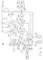
- a preferred amplifying apparatus 50comprises a first amplifier 60 for amplifying the 800 MHz signal, a second amplifier 80 for the 1900 MHz signal and a bias control circuit 100 .
- First amplifier 60comprises three amplifying stages 62 , 64 and 66 arranged as a cascade.
- An impedance network 68is connected to the input of first stage 62 , and it operates with first stage 62 to provide matching impedance to input 800 MHz signal 67 .
- an impedance network 70which provides, in conjunction with an inductor 75 , predetermined proper impedance between first stage 62 and second stage 64 for 800 MHz operation.
- Coupled between second stage 64 and third stage 66is an impedance network 72 which provides, in conjunction with another inductor 76 , proper predetermined impedance between second stage 64 and third stage 66 for the 800 MHz operation.
- the output of third stage 66is connected to an impedance network 74 which operates with third stage 66 and an inductor 79 to produce predetermined, desired load impedance for the 800 MHz operation.
- Amplifying stages 62 , 64 and 66are powered by a dc power supply +V DD through three choke inductors 75 , 76 and 79 , and an off-chip, on/off switch 77 .
- Three capacitors 81 , 83 and 85are used to provide ac ground to the power supply.
- Inductors 75 , 76 and 79will effect the interstage impedance and the output impedance. If the inductance of inductors 75 , 76 and 79 is large, however, their effect on the interstage impedance and the output impedance is negligible.
- Second amplifier 80 for amplifying the 1900 MHz signalcomprises three cascade amplifying stages 82 , 84 and 86 .
- the input of amplifying stage 82is connected to an impedance network 88 which operates with amplifying stage 82 to provide impedance that matches source impedance for the 1900 MHz operation.
- an impedance network 94operates with third stage 86 and an inductor 97 to provide predetermined, desired output impedance for the 1900 MHz operation.
- Impedance networks 90 and 92 and inductors 95 , 96 and 97provide predetermined, desired inter-stage impedance for 1900 MHz operation.
- the impedance value of network 90 at 1900 MHzis such that matching impedance between stages 82 and 84 is achieved.
- the impedance of impedance network 92is such that matching impedance between amplifying stages 84 and 86 are obtained at around 1900 MHz.
- Second amplifier 80is also powered by the dc power supply +V DD through a switch 77 and three choke inductors 96 . Capacitors 98 , 99 and 101 are used to provide AC ground to the power supply.
- Bias control circuit 100is connected to both amplifiers 60 and 80 . In addition to selectively enabling one of amplifiers 60 and 80 to operate while preventing the other amplifier from operation, control circuit 100 also provides a predetermined bias to the selected one amplifier to bias it to a desired mode of operation. Bias control circuit 100 is connected to a switch 108 at a terminal 102 for receiving a control signal. A positive power supply V DB is provided to control circuit 100 at a terminal 104 , and a negative dc power supply V SS is provided to control circuit 100 at a terminal 106 .
- Amplifying apparatus 50operates as follows: For 800 MHz operation, switch 108 is connected to terminal 110 at which a reference voltage for 800 MHz operation is provided. Responsive to this reference voltage, bias control circuit 100 provides a negative voltage to three amplifying stages 82 , 84 and 86 in the second amplifier to turn off these stages. At the same time, a proper bias is provided to amplifying stages 62 , 64 and 66 for them to operate in a desired mode. The amplifying apparatus is thus ready for 800 MHz operation.
- switch 108For 1900 MHz operation, switch 108 is connected to terminal 112 where a reference voltage for 1900 MHz operation is provided. In response to the reference voltage, bias control circuit 100 provides a negative bias to turn off the amplifying stages in first amplifier 60 . A desired bias for the 1900 MHz operation is provided to second amplifier 80 by bias control circuit 100 .
- a portion 114 of amplifying apparatus 50is in the form of a GaAs monolithic microwave integrated circuit (“MMIC”). More preferably, depletion-mode GaAs field effect transistors are used for signal amplification.
- MMICmonolithic microwave integrated circuit
- FIGS. 3A and 3Btogether illustrate a part-schematic circuit, part-block diagram of a preferred embodiment of the multi-band amplifier of FIG. 2 .
- the first two amplifying stagesincludes a depletion mode GaAs MESFET, and the last stage includes two depletion mode GaAs MESFETs for improved output power level.
- the circuit depicted in FIGS. 3A and 3Bis merely an example and not a limitation.
- an amplifying apparatusis provided with at least one amplifying stage and input impedance means.
- the input impedance meansprovide, in accordance with the frequency of input signal, predetermined input impedance at the frequency of the input signal.
- predetermined input impedanceis the impedance that matches source impedance.
- Source impedanceis the impedance of the signal source.
- the amplifying apparatusfurther includes output impedance means for providing, in accordance with the frequency of the signal, predetermined output impedance at the frequency of the input signal.
- output impedance meansfor providing, in accordance with the frequency of the signal, predetermined output impedance at the frequency of the input signal.
- a circuit for selectively biasing the amplifying stage to operate in a predetermined modeis also provided.
- An amplifying apparatus 150includes a single amplifying stage 152 having an input node 154 and an output node 156 .
- Input node 154is connected to a switch 158 which is selectively connected to either input impedance network 160 or 162 .
- Output node 156is connected to a switch 164 for selectively coupling to either output impedance network 166 or 168 .
- Input signal 174 of a first frequencyis received by the amplifying apparatus at a terminal 170 connected to impedance network 160 .
- Input signal of a second frequencyis received at a terminal 172 connected to impedance network 162 .
- 800 MHz and 1900 MHzare used here to represent the 800 MHz cellular band and the 1900 MHz PCS band; they are also referred here as the 800 MHz operation and the 1900 MHz operation.
- the amplifying apparatus of the present inventioncan be adapted to operate at other frequencies or frequency bands, or at more than two frequencies, which are all within the scope of the present invention.
- Amplifying apparatus 150provides output signal at 800 MHz, through an output impedance matching network 168 , at output terminal 178 .
- a 1900 MHz output signalis provided, through output impedance network 166 , at an output terminal 180 .
- Amplifying apparatus 150receives dc power from a dc power supply +V DD through an impedance network 182 .
- a bias control circuit 184is used to selectively bias the amplifying stage to operate in a desired mode. For example, amplifying stage 152 can be biased for class A, B, AB or C operation.
- Predetermined impedance for 800 MHz operationis provided by impedance networks 160 , 168 and 182 in conjunction with amplifying stage 152 . More specifically, input impedance networks 160 operating in conjunction with amplifying stage 152 provides input impedance that approximately matches source impedance at 800 MHz. Predetermined output impedance is provided for the 800 MHz operation by output impedance network 168 in conjunction with amplifying stage 152 and impedance network 182 . If the impedance of network 182 is large (such as a large choke inductor), its effect on the output impedance is negligible and the output impedance of amplifying apparatus 150 is mainly determined by output impedance network 168 and amplifying stage 152 .
- impedance networks 162 , 166 and 182in conjunction with amplifying stage 152 .
- Input impedance matching source impedance at 1900 MHzis obtained by impedance network 162 operating in conjunction with amplifying stage 152 .
- Predetermined output impedance for the 1900 MHz operationis achieved by impedance networks 166 and 182 operating in conjunction with amplifying stage 152 .
- impedance networkor “impedance matching network” is used here to refer to any electronic component or circuit thereof that displays a predetermined impedance at a frequency. It includes, without limitation, passive components, such as capacitors, resistors and inductors, and active components, such as transistors, diodes and circuits thereof.
- Amplifying apparatus 150operates as follows: For the 800 MHz operation, the input of amplifying stage 152 is connected to impedance network 160 , and the output of the amplifier is connected to impedance network 168 . A desired bias is provided to amplifying stage 152 by bias circuit 184 . If the input signal is at 1900 MHz, impedance networks 162 and 166 are connected to the input and output of amplifying stage 152 , respectively, and a desired bias for the 1900 MHz operation is provided to amplifying stage 152 by bias circuit 184 .
- FIG. 4depicts a dual-band amplifier
- an amplifying apparatus for more than two bandscan also be provided in accordance with the present invention, which is within the scope of the present invention.
- FIG. 4illustrates an example for providing predetermined input and output impedance for different frequency operations by using switching input impedance networks and switching output impedance networks.
- predetermined input and output impedanceaccording to the signal frequency, which are all within the scope of the present invention.
- FIG. 5Ais the block diagram of an alternative embodiment wherein like elements are similarly designated as FIG. 4 .
- switches 190 and 194are closed, and switches 192 and 196 are open.
- switches 192 and 196are closed and switches 190 and 194 are open.
- FIG. 5Billustrates another alternative embodiment.
- Amplifying stage 152is coupled to the dc power supply +V DD through one of two output impedance networks 198 and 200 by a switch 202 .
- An impedance network 204is connected to the output of the amplifying stage.
- Predetermined output impedance at 800 MHzis provided by connecting a switch 202 to impedance network 198 for the 800 MHz operation.
- Predetermined output impedance at 1099 MHzis provided by connecting switch 202 to impedance network 200 .
- predetermined output impedance for different frequency applicationsis obtained by switchably connecting impedance network 198 or 202 to the power supply.
- impedance network 198 or 202As is well known to those of skill in the art, an impedance component connected to the dc power supply in the shown fashion has a direct effect on the output impedance of the amplifying stage.
- the impedance values for impedance networks 198 , 200 and 204need to be such that desired output impedance for the 800 MHz or 1900 MHz operation is provided.
- FIG. 5Cis a block diagram depicting yet another way of providing predetermined input and output impedance for different frequency or frequency band operations.
- input of amplifying stage 152is connected to two impedance networks 208 and 210 connected in series.
- a switch 206is connected across impedance network 210 and when closed, it shorts network 210 .
- the output of amplifying stage 152is connected to two impedance networks 214 and 216 connected in series, with a switch 212 connected across network 214 .
- This amplifying apparatusoperates as follows: Both switches 206 and 212 are open for the 800 MHz operation.
- predetermined input impedancee.g., about 50 ohms
- impedance networks 208 and 210operating in conjunction with amplifying stage 152 .
- predetermined output impedancee.g., about 5 ohms
- impedance network 214 and 216operating in conjunction with amplifying stage 152 and impedance network 182 . If impedance network 182 has a large impedance, its effect on the output impedance is negligible and the output impedance is mainly determined by networks 214 and 216 and amplifying stage 152 .
- Both switches 206 and 212are closed for the 1900 MHz operation, shorting impedance networks 210 and 214 .
- predetermined input impedancee.g., about 50 ohms
- Predetermined output impedancee.g., about 5 ohms
- impedance networks 216 and 182 and amplifying stage 152are maintained by impedance networks 216 and 182 and amplifying stage 152 .
- input impedance networks 208 and 210can be such that predetermined, different input impedance for the 800 MHz and 1900 MHz operations be obtained. Similarly, predetermined, different output impedance for the 800 MHz and 1900 MHz operations can also be obtained.
- FIG. 5Ddepicts another alternative embodiment wherein two pairs of switching impedance networks are used for providing desired, predetermined output impedance for different frequency operations.
- a switch 158is connected to an impedance network 160 which, in conjunction with amplifying stage 152 , provides predetermined input impedance for the 800 MHz operation.
- a switch 226connects to an impedance network 218 and a switch 228 connects to an impedance network 222 ; impedance networks 218 and 222 provide, with the amplifying stage, predetermined output impedance for the 800 MHz operation.
- switch 158connects to an impedance network 162
- switch 226connects to an impedance network 22
- switch 228connects to an impedance network 224 ; the impedance values of these networks are such that desired input and output impedance is provided for the 1900 MHz operation.
- frequency filters/impedance networksare also used in providing predetermined input and output impedance for different frequency operations.
- a low-pass filter/impedance network 230 and a high-pass filter/impedance network 232are connected to the output of amplifying stage 152 .
- low-pass filter/impedance network 230allows 800 MHz signal to pass through and provides predetermined output impedance within the 800 MHz band.
- high-pass filter/impedance network 232which provides predetermined output impedance within the 1900 MHz band.
- Low pass and high pass filterscan also be used in a similar fashion at the input end of the amplifying stage (not shown), which is within the scope of the present invention.
- the amplifying apparatus described thus farcontains a single amplifying stage.
- a multiple stage amplifierin addition to providing predetermined input impedance and output impedance, it is also required that proper impedance between successive stages be provided.
- the output impedance of a preceding stageapproximately matches the input impedance of a following stage.
- impedance matching between stagesis not critical since sufficient gain is easily obtained even without interstage impedance matching. In fact, interstage impedance mismatching may be desired in certain instances to reduce the gain.
- impedance matching between stagesis important.
- predetermined impedance between successive stages of an amplifieris provided for different frequency operations.
- FIG. 6Ais a block diagram of a multi-stage amplifying apparatus 240 in accordance with the present invention.
- the apparatusincludes three amplifying stages: a first stage 242 , a second stage 244 , followed by an output stage 246 .
- a switch 249Connected to the input of first amplifying stage 242 is a switch 249 , which switchably connects to an impedance network 248 or 250 .
- switch 249connects to impedance network 248 which operates in conjunction with first amplifying stage 242 to provide predetermined input impedance.
- Switch 249connects to impedance network 250 for the 1900 MHz operation which operates in conjunction with first amplifying stage 242 to provide desired input impedance for the 1900 MHz operation.
- the input impedance provided by impedance network 248 or 250is about 50 ohms to match source impedance.
- Proper interstage impedance between first and second stagesis provided with the use of switches 255 and 261 and impedance networks 254 , 256 , 260 and 262 .
- switch 255connects to network 254 which, together with impedance network 252 and first amplifying stage 242 , provides predetermined interstage impedance suitable for the 800 MHz operation.
- Switch 255connects to impedance network 256 for the 1900 MHz operation, which, together with impedance network 252 and first amplifying apparatus 242 , provides predetermined interstage impedance.
- the output impedance of first stage 242approximately matches the input impedance of second stage 244 .
- predetermined interstage impedance between second amplifying stage 244 and third amplifying stage 246is provided by connecting switch 261 to impedance network 260 for the 800 MHz operation, or to impedance network 262 for the 1900 MHz operation.
- FIG. 6Bis a part-block and part-schematic diagram depicting a more preferred embodiment of the amplifying apparatus of FIG. 6 A. Like elements in this drawing are similarly designated as in FIG. 6 A.
- Two depletion mode GaAs FETs 270 and 272are used to form a switch 249 , and they are controlled by proper voltages applied to their gate terminals. For the 800 MHz operation, FET 270 is turned on and PET 272 is turned off. Conversely, for the 1900 MHz operation, FET 270 is ted off and FET 272 is turned on.
- this embodimentuses two depletion mode GaAs FETs 270 and 272 to form switch 249 , it will be apparent to one of ordinary skill in the art that other devices such as PN diodes, Schottky diodes, or preferably, PIN diodes can be used instead of the GaAs FETs to form the switch, which are all within the scope of the present invention.
- An output stage 246includes two depletion mode GaAs FETs connected in parallel. The drain terminals of the two FETs are biased by a dc power supply +V DD through one of two inductors 82 and 90 , which is selectively connected to the drain terminals by a switch 265 . This two FET type stage provides improved output power capability.
- depletion mode GaAs FETsare used as amplifying transistors in all three stages. It will be apparent to one of skill in the art that other kinds of transistors such as bipolar transistors or enhancement mode GaAs FETs can be used instead of the GaAs FETs, which are all within the scope of the present invention.
- FIG. 7Ais the block diagram of another alternative embodiment of the amplifying apparatus of FIG. 6 A.
- the output stage of this embodimentincludes two substages 282 and 284 for the 800 MHz or 1900 MHz operation, respectively. Depending on the frequency of operation, only one of the two substages is selectively activated and the selection is made by a switch 268 .
- switch 268is connected to substage 282 which provides predetermined output impedance at its output while substage 284 is turned off.
- Switch 268connects to substage 284 for the 1900 MHz operation, which provides proper output impedance for the 1900 MHz operation while substage 282 is turned off.
- FIG. 7Bis a part-block and part-schematic diagram of a more preferred embodiment of the amplifying apparatus of FIG. 7 A.
- two FETs 290 and 292are used as a switch for the output stage.
- V G1 and V G2By applying appropriate gate bias voltages V G1 and V G2 , a desired substage is selected.
- substage 284is electrically disconnected from the second stage by applying a gate bias V G2 of a negative voltage sufficient to turn off FET 292 .
- substage 282is electrically connected to the second stage by a gate bias V G1 which turns on FET 290 .
- substage 282 disconnected by turning off FET 290 and substage 284is selected by turning on FET 292 .
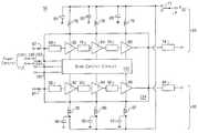
- FIG. 8depicts the block diagram of a preferred multi-band amplifying apparatus 300 of the present invention.
- Amplifying apparatus 300includes a GaAs MMIC power amplifier chip 302 and a number of off-chip components. In the GaAs power amplifier chip, three amplifying stages 304 , 306 and 308 are connected as a cascade through impedance networks 310 and 312 .
- a switch 316is connected to the input of first stage 304 through an impedance network 314 and it selectively connects to either an impedance network 318 or an impedance network 320 .
- Impedance network 318receives input 800 MHz signal at a terminal 322 .
- Impedance network 320receives input 1900 MHz signal at a terminal 324 .
- switch 316When switch 316 connects to impedance network 318 , predetermined input impedance for the 800 MHz operation is provided at input terminal 322 .
- Switch 316connects to impedance network 320 for the 1900 MHz operation; impedance network 320 operates with first stage 304 to provide predetermined input impedance for the 1900 MHz operation.
- Two switching impedance networksare used to provide predetermined output impedance for the 800 MHz or 1900 MHz operation. More specifically, the output of the third stage is connected to an off-chip switch 328 , which is selectively connected to either an off-chip impedance network 330 for the 800 MHz operation or an off-chip impedance network 332 for the 1900 MHz operation. The output of the third stage is also connected to an off-chip impedance network 326 to receive the dc power +V DD .
- switch 328connects to impedance network 330
- predetermined output impedance for the 800 MHz operationis provided at a terminal 334 by impedance networks 330 and 326 operating in conjunction with third stage 308 .
- switch 328is connected to impedance network 332 and predetermined output impedance is provided at terminal 336 by impedance networks 332 and 326 operating in conjunction with third stage 308 .
- Predetermined inter-stage impedance for different frequency operationsis obtained in this amplifying apparatus by using switching impedance networks. More specifically, first stage 304 is connected to the dc power supply +V DD via an on-chip impedance network 340 and an off-chip impedance network 342 . Connected across impedance network 340 is an on-chip electronic switch 338 which, if closed, shorts impedance network 340 . For the 800 MHz operation, switch 338 is open and predetermined, proper interstage impedance between first amplifying stage 304 and second amplifying stage 306 for the 800 MHz operation is provided by impedance networks 310 , 340 and 342 .
- impedance networks 342 and 310When the apparatus operates within the 1900 MHz band, switch 338 is closed, shorting impedance network 340 . At this time, predetermined, proper interstage impedance between first amplifying stage 304 and second stage 306 is provided by impedance networks 342 and 310 . Preferably, the impedance values of impedance networks 342 and 310 are such that matching impedance between the first and second stage is obtained for the 1900 MHz operation.
- Predetermined inter-stage impedance between second amplifying stage 306 and third amplifying stage 308 for the 800 MHz or 1900 MHz operationis similarly obtained with the use of on-chip impedance networks 312 and 344 , an on-chip electronic switch 348 and an off-chip impedance network 346 .
- Switch 348is open for the 800 MHz operation, and it is closed for the 1900 MHz operation.
- GaAs MMIC power amplifier chip 302further includes an on-chip control circuit 350 for controlling electronic switches 316 , 338 and 348 .
- the dash lines connecting these switches to control circuit 350illustrate the control of these switches by control circuit 350 .
- control circuit 350For the 800 MHz operation, responding to a control signal V C received from an off-chip source, control circuit 350 causes switch 316 to connect to impedance network 318 , and opens switches 338 and 348 .
- V Ctriggers the control circuit to generate proper signals to control those switches; it can be, by example and not limitation, a signal responsive to a cellular base station.
- GaAs MMIC power amplifier chip 302further includes a bias control circuit 352 for providing appropriate bias to amplifying stages 304 , 306 and 308 .
- a bias control circuit 352for providing appropriate bias to amplifying stages 304 , 306 and 308 .
- amplifying stage 304 , 306 and 308can be biased for A, B, AB or C operation.
- Bias control circuit 352is connected to a number of off-chip voltages: a positive voltage supply V DB , a negative voltage supply V SS , and a reference voltage V REF .
- Reference voltage V Refis provided to bias control circuit 352 through a switch 354 .
- Bias control circuit 352can also be connected to two pairs of optional bias resistors through two off-chip electronic switches 356 and 358 .
- the optional bias resistorsare used to form, with on-chip resistors, a voltage divider by which the bias voltage can be adjusted by judiciously choosing the resistance values of these optional bias resistors.
- the output of third amplifying stage 308is connected to a low-pass impedance network 360 and a high-pass impedance network 362 .
- the 800 MHz signalwill pass the low-pass impedance network which provides predetermined output impedance for the 800 MHz operation.
- the 1900 MHz signalwill pass the high-pass impedance network 362 which provides predetermined output impedance for the 1900 MHz operation.
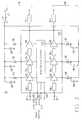
- FIG. 10is a partial schematic circuit diagram of a preferred GaAs MMIC circuit 302 of FIG. 8., excluding control circuit 350 and bias control circuit 352 .
- This preferred GaAs MMICincludes three amplifying stages: a first stage including a depletion-mode GaAs power FET 600 , a second stage including a depletion-mode GaAs power FET 602 , and a third stage including two depletion-mode GaAs FETs 604 and 606 connected in parallel.
- Two input signals, 800 MHz signal and 1900 MHz signalare provided at terminals 608 and 610 , respectively.
- Two depletion-mode GaAs FETs 612 and 614controlled by a control circuit (shown in FIG. 12 ), function to selectively provide either the 800 MHz signal or the 1900 MHz signal to the first amplifying stage.
- the control circuitapplies appropriate control voltages V C1 and V C2 through conductors 616 and 618 to the gate of FETs 612 and 614 to cause the FETs to turn on or off.
- the control circuitalso control FETs 620 and 622 which function as switches for providing predetermined inter-stage impedance.
- GaAs power FETs 600 , 602 , and 604 and 606are biased by a bias control circuit (shown in FIG. 11) at terminals 624 , 626 and 628 .
- Bias voltages applied to the three terminalsare designated as V G1 , V G2 and V G3 .
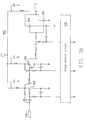
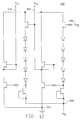
- FIG. 11is a schematic circuit diagram of a preferred bias control circuit 623 .
- Bias control circuit 623comprises three depletion mode GaAs FETs 630 , 632 and 634 .
- a positive dc power source +V DB and a negative power source ⁇ V SSare connected to the bias control circuit.
- a reference voltage V Refis also applied to the gate of FET 632 .
- Bias circuit 623provides a bias voltage at a terminal 636 that is connected to the amplifying circuit of FIG. 10 at terminals 624 (V G1 ), 626 (V G2 ) and 628 (V G3 ).
- bias control circuit 623is a part of a GaAs MMIC which includes the amplifying circuit of FIG. 10 and the bias control circuit of FIG. 11 . It will be apparent to one of ordinary skill in the art that other bias circuits different from the one depicted in FIG. 11, can also be used in place of bias control circuit 623 described above.
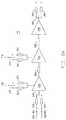
- a control circuit 640is connected to ground at a terminal 644 and to a negative power source ⁇ V SS at a terminal 642 .
- An external control voltage V Cis provided to the control circuit at a terminal 646 .
- Control voltages V C1 and V C2are provided at terminals 648 and 650 , respectively.
- control circuit 640is formed with amplifying circuit 302 depicted in FIG. 10 and bias control circuit 623 depicted in FIG. 11 as a GaAs MMIC.
- control circuit 640operates as follows: When V C is a low voltage such as ground, V C1 is low and V C2 is high and as a result, amplifying circuit 302 is set up for the 800 MHz operation. Conversely, if V C is high, then V C1 becomes high and V C2 is low; amplifying circuit 302 is ready for the 1900 MHz operation.
- FIG. 13illustrates an alternative way for providing predetermined output impedance for different frequency operations. For simplicity, only the last stage is illustrated.
- Last stage 652is connected to two impedance networks 654 and 656 .
- Capacitors 658 and 660are coupled to ground through two switches 662 and 664 , respectively.
- the apparatus of FIG. 13operates as follows: for the 1900 MHz operation, switch 662 is closed and switch 664 is open; impedance networks 654 and 656 and capacitor 658 operate in conjunction with stage 652 to provide predetermined, desired output impedance for the 1900 MHz operation.
- switch 662is open and switch 664 is closed, and the two impedance networks and capacitor 664 operate in conjunction with stage 652 to provide predetermined, desired output impedance for the 800 MHz operation.
Landscapes
- Engineering & Computer Science (AREA)
- Power Engineering (AREA)
- Computer Networks & Wireless Communication (AREA)
- Signal Processing (AREA)
- Amplifiers (AREA)
- Microwave Amplifiers (AREA)
- Mobile Radio Communication Systems (AREA)
Abstract
Description
Claims (39)
Priority Applications (1)
| Application Number | Priority Date | Filing Date | Title |
|---|---|---|---|
| US09/821,177US6501331B2 (en) | 1996-06-03 | 2001-03-29 | Multi-band amplifier |
Applications Claiming Priority (3)
| Application Number | Priority Date | Filing Date | Title |
|---|---|---|---|
| US08/664,972US5774017A (en) | 1996-06-03 | 1996-06-03 | Multiple-band amplifier |
| US09/080,786US6242986B1 (en) | 1996-06-03 | 1998-05-18 | Multiple-band amplifier |
| US09/821,177US6501331B2 (en) | 1996-06-03 | 2001-03-29 | Multi-band amplifier |
Related Parent Applications (1)
| Application Number | Title | Priority Date | Filing Date |
|---|---|---|---|
| US09/080,786ContinuationUS6242986B1 (en) | 1996-06-03 | 1998-05-18 | Multiple-band amplifier |
Publications (2)
| Publication Number | Publication Date |
|---|---|
| US20010011926A1 US20010011926A1 (en) | 2001-08-09 |
| US6501331B2true US6501331B2 (en) | 2002-12-31 |
Family
ID=24668195
Family Applications (3)
| Application Number | Title | Priority Date | Filing Date |
|---|---|---|---|
| US08/664,972Expired - LifetimeUS5774017A (en) | 1996-06-03 | 1996-06-03 | Multiple-band amplifier |
| US09/080,786Expired - LifetimeUS6242986B1 (en) | 1996-06-03 | 1998-05-18 | Multiple-band amplifier |
| US09/821,177Expired - LifetimeUS6501331B2 (en) | 1996-06-03 | 2001-03-29 | Multi-band amplifier |
Family Applications Before (2)
| Application Number | Title | Priority Date | Filing Date |
|---|---|---|---|
| US08/664,972Expired - LifetimeUS5774017A (en) | 1996-06-03 | 1996-06-03 | Multiple-band amplifier |
| US09/080,786Expired - LifetimeUS6242986B1 (en) | 1996-06-03 | 1998-05-18 | Multiple-band amplifier |
Country Status (2)
| Country | Link |
|---|---|
| US (3) | US5774017A (en) |
| JP (1) | JPH1065466A (en) |
Cited By (35)
| Publication number | Priority date | Publication date | Assignee | Title |
|---|---|---|---|---|
| US20030214352A1 (en)* | 2002-05-20 | 2003-11-20 | Alps Electric Co., Ltd. | Power amplifier capable of adjusting operating point |
| US20040201423A1 (en)* | 2003-04-14 | 2004-10-14 | M/A-Com, Inc. | Handset radiofrequency front end module in fine pitch quad flat no lead (FQFP-N) package |
| US20040227576A1 (en)* | 2003-05-15 | 2004-11-18 | Vice Michael W. | Equal phase multiple gain state amplifier |
| US20040232993A1 (en)* | 2003-05-20 | 2004-11-25 | En-Hsiang Yeh | Multi-band low noise amplifier |
| US20050156671A1 (en)* | 2004-01-20 | 2005-07-21 | Shanjani Payman H. | Method and apparatus for compensating and improving efficiency in a variable power amplifier |
| US20050189989A1 (en)* | 2004-02-19 | 2005-09-01 | Sony Corporation | Power amplification apparatus, and mobile communication terminal apparatus |
| US20060035667A1 (en)* | 2004-08-10 | 2006-02-16 | Lg Electronics Inc. | Multi band mobile communications terminal |
| US20060055445A1 (en)* | 2002-07-24 | 2006-03-16 | Sirific Wireless Corporation | Multi-standard amplifier |
| US20060246857A1 (en)* | 2003-03-27 | 2006-11-02 | Giuseppe Grillo | Power saving in a transmitter |
| US7184723B2 (en) | 2004-10-22 | 2007-02-27 | Parkervision, Inc. | Systems and methods for vector power amplification |
| US20070155345A1 (en)* | 2005-12-12 | 2007-07-05 | Alcatel | Frequency switch for multiband power amplifier applications and multiband/multistandard power amplifier module |
| US7355470B2 (en) | 2006-04-24 | 2008-04-08 | Parkervision, Inc. | Systems and methods of RF power transmission, modulation, and amplification, including embodiments for amplifier class transitioning |
| US7620129B2 (en) | 2007-01-16 | 2009-11-17 | Parkervision, Inc. | RF power transmission, modulation, and amplification, including embodiments for generating vector modulation control signals |
| US7885682B2 (en) | 2006-04-24 | 2011-02-08 | Parkervision, Inc. | Systems and methods of RF power transmission, modulation, and amplification, including architectural embodiments of same |
| US7911272B2 (en) | 2007-06-19 | 2011-03-22 | Parkervision, Inc. | Systems and methods of RF power transmission, modulation, and amplification, including blended control embodiments |
| US7982543B1 (en) | 2009-03-30 | 2011-07-19 | Triquint Semiconductor, Inc. | Switchable power amplifier |
| US7990212B1 (en)* | 2009-12-18 | 2011-08-02 | Cirrus Logic, Inc. | Modulated audio amplifier output enable control |
| US8013675B2 (en) | 2007-06-19 | 2011-09-06 | Parkervision, Inc. | Combiner-less multiple input single output (MISO) amplification with blended control |
| US20110234316A1 (en)* | 2010-03-26 | 2011-09-29 | Avago Technologies Wireless Ip (Singapore) Pte. Ltd. | Impedance matching circuit capable of efficiently isolating paths for multi-band power amplifier |
| US8031804B2 (en) | 2006-04-24 | 2011-10-04 | Parkervision, Inc. | Systems and methods of RF tower transmission, modulation, and amplification, including embodiments for compensating for waveform distortion |
| US8207798B1 (en) | 2009-09-09 | 2012-06-26 | Triquint Semiconductor, Inc. | Matching network with switchable capacitor bank |
| US8315336B2 (en) | 2007-05-18 | 2012-11-20 | Parkervision, Inc. | Systems and methods of RF power transmission, modulation, and amplification, including a switching stage embodiment |
| US8334722B2 (en) | 2007-06-28 | 2012-12-18 | Parkervision, Inc. | Systems and methods of RF power transmission, modulation and amplification |
| US20130109434A1 (en)* | 2011-07-24 | 2013-05-02 | Ethertronics, Inc. | Multi-mode multi-band self-realigning power amplifier |
| US8755454B2 (en) | 2011-06-02 | 2014-06-17 | Parkervision, Inc. | Antenna control |
| US20150171804A1 (en)* | 2012-07-27 | 2015-06-18 | Soongsil University Research Consortium Techno- Park | Power amplifier having stack structure |
| US9106316B2 (en) | 2005-10-24 | 2015-08-11 | Parkervision, Inc. | Systems and methods of RF power transmission, modulation, and amplification |
| US9209762B1 (en) | 2013-04-01 | 2015-12-08 | Cirrus Logic, Inc. | Switching power amplifier with rate-controlled power supply voltage transitions |
| US9608677B2 (en) | 2005-10-24 | 2017-03-28 | Parker Vision, Inc | Systems and methods of RF power transmission, modulation, and amplification |
| US9716471B2 (en) | 2014-12-22 | 2017-07-25 | Raytheon Company | Quasi-switched, multi-band, high-power amplifier and method |
| US9871490B2 (en)* | 2012-07-13 | 2018-01-16 | Qorvo International Pte. Ltd. | Multi-band/multi-mode power amplifier with signal path hardware sharing |
| US10278131B2 (en) | 2013-09-17 | 2019-04-30 | Parkervision, Inc. | Method, apparatus and system for rendering an information bearing function of time |
| US20190131941A1 (en)* | 2017-10-31 | 2019-05-02 | Murata Manufacturing Co., Ltd. | Power amplifier circuit |
| US11601144B2 (en) | 2020-08-26 | 2023-03-07 | Skyworks Solutions, Inc. | Broadband architectures for radio frequency front-ends |
| US11671122B2 (en) | 2020-08-26 | 2023-06-06 | Skyworks Solutions, Inc. | Filter reuse in radio frequency front-ends |
Families Citing this family (138)
| Publication number | Priority date | Publication date | Assignee | Title |
|---|---|---|---|---|
| US6137355A (en)* | 1994-04-17 | 2000-10-24 | Sevic; John F. | Dual-mode amplifier with high efficiency and high linearity |
| US5774017A (en)* | 1996-06-03 | 1998-06-30 | Anadigics, Inc. | Multiple-band amplifier |
| US5973557A (en)* | 1996-10-18 | 1999-10-26 | Matsushita Electric Industrial Co., Ltd. | High efficiency linear power amplifier of plural frequency bands and high efficiency power amplifier |
| US6128508A (en)* | 1996-12-27 | 2000-10-03 | Lucent Technologies Inc. | Communications system using multi-band amplifiers |
| SE512927C2 (en)* | 1997-01-30 | 2000-06-05 | Ericsson Telefon Ab L M | Wireless terminal operating according to more than one air interface protocol |
| US6078794A (en)* | 1997-02-19 | 2000-06-20 | Motorola, Inc. | Impedance matching for a dual band power amplifier |
| US5995814A (en)* | 1997-06-13 | 1999-11-30 | Lucent Technologies Inc. | Single-stage dual-band low-noise amplifier for use in a wireless communication system receiver |
| US6188877B1 (en) | 1997-07-03 | 2001-02-13 | Ericsson Inc. | Dual-band, dual-mode power amplifier with reduced power loss |
| US6091966A (en)* | 1997-09-29 | 2000-07-18 | Ericsson, Inc. | Dual-band, dual-mode power amplifier |
| US6298244B1 (en)* | 1997-07-03 | 2001-10-02 | Ericsson Inc. | Dual-band, dual-mode power amplifier |
| US6127886A (en)* | 1997-10-30 | 2000-10-03 | The Whitaker Corporation | Switched amplifying device |
| US6216012B1 (en)* | 1997-11-07 | 2001-04-10 | Conexant Systems, Inc. | Dualband power amplifier control using a single power amplifier controller |
| US6075995A (en)* | 1998-01-30 | 2000-06-13 | Conexant Systems, Inc. | Amplifier module with two power amplifiers for dual band cellular phones |
| DE19811830C2 (en)* | 1998-03-18 | 2002-05-29 | Siemens Ag | Method for determining transmission errors in a serial data stream transmitted using a multi-carrier method |
| DE19823060C2 (en)* | 1998-05-22 | 2001-02-22 | Ericsson Telefon Ab L M | Power amplifier output circuit |
| US6628170B2 (en)* | 1998-06-04 | 2003-09-30 | Analog Devices, Inc. | Low noise amplifier |
| US6163709A (en)* | 1998-06-24 | 2000-12-19 | Conexant Systems, Inc. | Cellular phone with a logarithmic detector |
| US6151509A (en)* | 1998-06-24 | 2000-11-21 | Conexant Systems, Inc. | Dual band cellular phone with two power amplifiers and a current detector for monitoring the consumed power |
| US6154664A (en)* | 1998-06-24 | 2000-11-28 | Conexant System, Inc. | Dual band cellular phone with two power amplifiers and power control circuit therefore |
| DE69838212T3 (en)* | 1998-07-28 | 2019-03-14 | Ipcom Gmbh & Co. Kg | mobile phone |
| GB2341993B (en)* | 1998-09-25 | 2003-03-12 | Nec Technologies | Radio receivers |
| US6134427A (en)* | 1998-09-30 | 2000-10-17 | Conexant Systems, Inc. | Using a single low-noise amplifier in a multi-band wireless station |
| DE19846069A1 (en)* | 1998-10-06 | 2000-04-13 | Siemens Ag | Transmitter for a mobile phone |
| DE19854847C2 (en)* | 1998-11-27 | 2003-07-31 | Vishay Semiconductor Gmbh | amplifier arrangement |
| US6281755B1 (en)* | 1998-12-28 | 2001-08-28 | Siemens Aktiengesellschaft | High-frequency power amplifier |
| WO2000055967A1 (en)* | 1999-03-15 | 2000-09-21 | Matsushita Electric Industrial Co., Ltd. | Semiconductor device and communication device |
| US6118343A (en)* | 1999-05-10 | 2000-09-12 | Tyco Electronics Logistics Ag | Power Amplifier incorporating single drain switch and single negative voltage generator |
| US6194968B1 (en) | 1999-05-10 | 2001-02-27 | Tyco Electronics Logistics Ag | Temperature and process compensating circuit and controller for an RF power amplifier |
| DE19930195C2 (en)* | 1999-06-30 | 2001-08-30 | Siemens Ag | Circuit for amplifying a high-frequency signal from at least two high-frequency ranges, 2-band receiver with the circuit, 2-band mobile radio device with the receiver and use of a series circuit comprising a capacitive element and a high-frequency line in an amplifier circuit |
| WO2001005028A1 (en)* | 1999-07-07 | 2001-01-18 | Ericsson Inc. | A dual-band, dual-mode power amplifier |
| US6559722B1 (en)* | 1999-08-10 | 2003-05-06 | Anadigics, Inc. | Low bias current/temperature compensation current mirror for linear power amplifier |
| FR2798016B1 (en)* | 1999-08-31 | 2002-03-29 | St Microelectronics Sa | AMPLIFIER CIRCUIT WITH DOUBLE BANDWIDTH AND RADIO FREQUENCY RECEIVING HEAD |
| FI108196B (en)* | 1999-09-30 | 2001-11-30 | Nokia Networks Oy | Arrangement and method for realizing a transmitter-receiver function in a radio system |
| US6215355B1 (en)* | 1999-10-13 | 2001-04-10 | Tropian, Inc. | Constant impedance for switchable amplifier with power control |
| US6236274B1 (en) | 2000-01-04 | 2001-05-22 | Industrial Technology Research Institute | Second harmonic terminations for high efficiency radio frequency dual-band power amplifier |
| US6281748B1 (en) | 2000-01-14 | 2001-08-28 | Motorola, Inc. | Method of and apparatus for modulation dependent signal amplification |
| US6597925B1 (en)* | 2000-03-16 | 2003-07-22 | Agere Systems Inc. | Transmitter circuit with frequency self-optimization |
| US6658265B1 (en) | 2000-04-25 | 2003-12-02 | Rf Micro Devices, Inc. | Matching network for a dual mode RF amplifier |
| EP1156582A3 (en)* | 2000-05-16 | 2004-04-28 | Nokia Corporation | Transmitter/receiver chain impedance optimization |
| US7020450B2 (en)* | 2000-09-05 | 2006-03-28 | Nec Corporation | Active inductors using bipolar silicon transistors |
| US7123899B1 (en)* | 2000-09-06 | 2006-10-17 | Industrial Technology Research Institute | Broadband single-ended input upconverter |
| JP3895532B2 (en)* | 2000-09-11 | 2007-03-22 | 株式会社ルネサステクノロジ | High frequency power amplifier and wireless communication device |
| FI114261B (en)* | 2000-09-12 | 2004-09-15 | Nokia Corp | Transmitter and wireless communication device |
| JP2002111415A (en)* | 2000-09-29 | 2002-04-12 | Hitachi Ltd | High frequency power amplifier and wireless communication device |
| US6856199B2 (en)* | 2000-10-10 | 2005-02-15 | California Institute Of Technology | Reconfigurable distributed active transformers |
| EP1202467B1 (en)* | 2000-10-24 | 2004-07-07 | Koninklijke Philips Electronics N.V. | Signal transmitter with impulse control of amplification |
| FR2816472B1 (en)* | 2000-11-07 | 2004-10-15 | Sagem | MOBILE TELEPHONE WITH MULTIBAND TRANSMISSION DEVICE |
| AU2002254159A1 (en)* | 2001-03-09 | 2002-09-24 | California Institute Of Technology | Switchless multi-resonant, multi-band power amplifier |
| GB0107264D0 (en)* | 2001-03-22 | 2001-05-16 | Nokia Networks Oy | Processing signals in a transmitter |
| FR2825562B1 (en)* | 2001-05-30 | 2003-09-05 | Sagem | MULTIMODE PORTABLE TELEPHONE WITH SINGLE TRANSMISSION AMPLIFIER |
| TW486861B (en)* | 2001-07-04 | 2002-05-11 | Ind Tech Res Inst | Impedance matching circuit for a multi-band power amplifier |
| US6680652B2 (en) | 2001-08-06 | 2004-01-20 | Rf Micro Devices, Inc. | Load switching for transmissions with different peak-to-average power ratios |
| US6683496B2 (en)* | 2001-08-20 | 2004-01-27 | Harris Corporation | System and method for minimizing dissipation in RF power amplifiers |
| JP3877558B2 (en)* | 2001-09-11 | 2007-02-07 | 株式会社ルネサステクノロジ | High frequency power amplifier, high frequency power amplifier module, and mobile phone |
| US6985698B2 (en)* | 2001-11-14 | 2006-01-10 | Koninklijke Philips Electronics N.V. | Impedeance matching circuit for a multi-band radio frequency device |
| JP3932259B2 (en)* | 2001-12-12 | 2007-06-20 | 株式会社ルネサステクノロジ | High frequency power amplifier circuit and electronic component for wireless communication |
| JP3708869B2 (en)* | 2001-12-19 | 2005-10-19 | Nec化合物デバイス株式会社 | High frequency circuit |
| US7199056B2 (en)* | 2002-02-08 | 2007-04-03 | Applied Materials, Inc. | Low cost and low dishing slurry for polysilicon CMP |
| WO2003071699A1 (en)* | 2002-02-20 | 2003-08-28 | Koninklijke Philips Electronics N.V. | Mobile multimode terminal with joint power amplifier |
| ATE378731T1 (en)* | 2002-05-22 | 2007-11-15 | Siemens Spa Italiana | UP FREQUENCY CONVERTER FOR RADIO SYSTEMS |
| US6806767B2 (en) | 2002-07-09 | 2004-10-19 | Anadigics, Inc. | Power amplifier with load switching circuit |
| US7298854B2 (en)* | 2002-12-04 | 2007-11-20 | M/A-Com, Inc. | Apparatus, methods and articles of manufacture for noise reduction in electromagnetic signal processing |
| EP1550207A2 (en)* | 2002-10-08 | 2005-07-06 | M/A-Com, Inc. | Apparatus, methods and articles of manufacture for multiband signal processing |
| US6924699B2 (en)* | 2003-03-06 | 2005-08-02 | M/A-Com, Inc. | Apparatus, methods and articles of manufacture for digital modification in electromagnetic signal processing |
| US7203262B2 (en) | 2003-05-13 | 2007-04-10 | M/A-Com, Inc. | Methods and apparatus for signal modification in a fractional-N phase locked loop system |
| US6891432B2 (en)* | 2002-11-14 | 2005-05-10 | Mia-Com, Inc. | Apparatus, methods and articles of manufacture for electromagnetic processing |
| US7526260B2 (en)* | 2002-11-14 | 2009-04-28 | M/A-Com Eurotec, B.V. | Apparatus, methods and articles of manufacture for linear signal modification |
| US7187231B2 (en)* | 2002-12-02 | 2007-03-06 | M/A-Com, Inc. | Apparatus, methods and articles of manufacture for multiband signal processing |
| US7545865B2 (en)* | 2002-12-03 | 2009-06-09 | M/A-Com, Inc. | Apparatus, methods and articles of manufacture for wideband signal processing |
| US7245183B2 (en)* | 2002-11-14 | 2007-07-17 | M/A-Com Eurotec Bv | Apparatus, methods and articles of manufacture for processing an electromagnetic wave |
| JP4160365B2 (en)* | 2002-11-07 | 2008-10-01 | 株式会社ルネサステクノロジ | Electronic component for high frequency power amplification and wireless communication system |
| US6859098B2 (en) | 2003-01-17 | 2005-02-22 | M/A-Com, Inc. | Apparatus, methods and articles of manufacture for control in an electromagnetic processor |
| JP3892826B2 (en)* | 2003-05-26 | 2007-03-14 | 株式会社東芝 | Power amplifier and wireless communication apparatus using the same |
| EP1489750B1 (en)* | 2003-06-10 | 2008-03-05 | Sony Ericsson Mobile Communications AB | Reduction of radio frequency leakage |
| US7170341B2 (en)* | 2003-08-05 | 2007-01-30 | Motorola, Inc. | Low power consumption adaptive power amplifier |
| TW200518345A (en)* | 2003-08-08 | 2005-06-01 | Renesas Tech Corp | Semiconductor device |
| US7480511B2 (en)* | 2003-09-19 | 2009-01-20 | Trimble Navigation Limited | Method and system for delivering virtual reference station data |
| US7091778B2 (en) | 2003-09-19 | 2006-08-15 | M/A-Com, Inc. | Adaptive wideband digital amplifier for linearly modulated signal amplification and transmission |
| US7754539B2 (en)* | 2003-10-08 | 2010-07-13 | Sige Semiconductor Inc. | Module integration integrated circuits |
| US7409200B2 (en) | 2003-10-08 | 2008-08-05 | Sige Semiconductor Inc. | Module integration integrated circuits |
| US7149483B1 (en) | 2003-10-28 | 2006-12-12 | Magnolia Broadband Inc. | Amplifying diversity signals using power amplifiers |
| US6970040B1 (en)* | 2003-11-13 | 2005-11-29 | Rf Micro Devices, Inc. | Multi-mode/multi-band power amplifier |
| JP4867346B2 (en)* | 2003-11-13 | 2012-02-01 | 日本電気株式会社 | High frequency amplifier |
| KR100565306B1 (en) | 2003-11-22 | 2006-03-30 | 엘지전자 주식회사 | Amplification offset adjusting device of mobile communication receiver |
| US7343138B2 (en)* | 2003-12-08 | 2008-03-11 | M/A-Com, Inc. | Compensating for load pull in electromagentic signal propagation using adaptive impedance matching |
| US20060194551A1 (en)* | 2005-02-25 | 2006-08-31 | Matsushita Electric Industrial Co., Ltd. | Power amplifier and polar modulation system |
| JP2006262240A (en)* | 2005-03-18 | 2006-09-28 | Sony Ericsson Mobilecommunications Japan Inc | Power amplification device and mobile phone terminal |
| US7164319B2 (en)* | 2005-04-29 | 2007-01-16 | Triquint Semiconductor, Inc. | Power amplifier with multi mode gain circuit |
| US7345534B2 (en)* | 2005-05-31 | 2008-03-18 | M/A-Com Eurotec Bv | Efficient power amplification system |
| US7508249B2 (en)* | 2005-07-27 | 2009-03-24 | Analog Devices, Inc. | Distributed transistor structure for high linearity active CATV power splitter |
| US7826810B2 (en)* | 2006-05-08 | 2010-11-02 | Harris Corporation | Multiband radio with transmitter output power optimization |
| JP2007312031A (en)* | 2006-05-17 | 2007-11-29 | Matsushita Electric Ind Co Ltd | Electronic devices |
| JP4957095B2 (en)* | 2006-06-29 | 2012-06-20 | 富士通株式会社 | Multiband high frequency amplifier |
| JP2008154201A (en)* | 2006-07-07 | 2008-07-03 | Murata Mfg Co Ltd | Transmitter |
| JP4840053B2 (en)* | 2006-09-29 | 2011-12-21 | ソニー株式会社 | Power amplifier |
| US7869775B2 (en)* | 2006-10-30 | 2011-01-11 | Skyworks Solutions, Inc. | Circuit and method for biasing a gallium arsenide (GaAs) power amplifier |
| JP2008288769A (en)* | 2007-05-16 | 2008-11-27 | Panasonic Corp | High frequency circuit, semiconductor device, and high frequency power amplifier |
| US7936045B2 (en)* | 2007-06-11 | 2011-05-03 | Infineon Technologies Ag | Integrated circuit with multi-stage matching circuit |
| EP2053738A1 (en)* | 2007-10-25 | 2009-04-29 | Alcatel Lucent | Amplifier with adjustable frequency band |
| US7853290B2 (en)* | 2007-10-29 | 2010-12-14 | Infineon Technologies Ag | Transmitter arrangement |
| US8718582B2 (en)* | 2008-02-08 | 2014-05-06 | Qualcomm Incorporated | Multi-mode power amplifiers |
| KR100948029B1 (en) | 2008-02-29 | 2010-03-19 | 인하대학교 산학협력단 | Dual Band Power Amplifier |
| US8099127B2 (en)* | 2008-08-01 | 2012-01-17 | Qualcomm Incorporated | Multi-mode configurable transmitter circuit |
| EP2178219B1 (en)* | 2008-10-20 | 2011-06-08 | Alcatel Lucent | A method for broadband matching and a network element thereof |
| CN102640350B (en)* | 2009-02-18 | 2015-02-04 | 豪沃基金有限责任公司 | Metamaterial Power Amplifier System |
| US8379548B1 (en)* | 2009-03-06 | 2013-02-19 | Qualcomm Incorporated | Architecture for simultaneous transmission of multiple protocols in a wireless device |
| US9143172B2 (en)* | 2009-06-03 | 2015-09-22 | Qualcomm Incorporated | Tunable matching circuits for power amplifiers |
| US8963611B2 (en)* | 2009-06-19 | 2015-02-24 | Qualcomm Incorporated | Power and impedance measurement circuits for a wireless communication device |
| JP2011015242A (en)* | 2009-07-02 | 2011-01-20 | Panasonic Corp | Radio frequency power amplifier |
| US8750810B2 (en)* | 2009-07-24 | 2014-06-10 | Qualcomm Incorporated | Power amplifier with switched output matching for multi-mode operation |
| US8072272B2 (en) | 2009-08-19 | 2011-12-06 | Qualcomm, Incorporated | Digital tunable inter-stage matching circuit |
| US9559639B2 (en)* | 2009-08-19 | 2017-01-31 | Qualcomm Incorporated | Protection circuit for power amplifier |
| JP2011135282A (en)* | 2009-12-24 | 2011-07-07 | Tdk Corp | Power amplifier circuit |
| JP2012049909A (en)* | 2010-08-27 | 2012-03-08 | Toshiba Corp | Wide band power amplifier |
| EP2432121B1 (en)* | 2010-09-15 | 2014-03-19 | Sony Ericsson Mobile Communications AB | Broadband power amplifier |
| WO2012040879A1 (en)* | 2010-09-30 | 2012-04-05 | Telefonaktiebolaget Lm Ericsson (Publ) | Multi-band switched-mode power amplifier |
| KR101250720B1 (en)* | 2010-12-21 | 2013-04-03 | 삼성전기주식회사 | Antenna switch circuit and switching method thereof |
| US20120280755A1 (en)* | 2011-05-04 | 2012-11-08 | Triquint Semiconductor, Inc. | Flip-chip power amplifier and impedance matching network |
| JPWO2013150564A1 (en)* | 2012-04-04 | 2015-12-14 | 三菱電機株式会社 | Multimode multiband amplifier |
| KR101332569B1 (en) | 2012-11-20 | 2013-11-25 | 숭실대학교산학협력단 | Differential multistage distributed amplifier |
| FR3002708A1 (en)* | 2013-02-28 | 2014-08-29 | Thales Sa | SIGNAL AMPLIFICATION SYSTEM |
| US9312821B2 (en)* | 2013-05-07 | 2016-04-12 | Maxlinear, Inc. | Method and system for a configurable low-noise amplifier with programmable band-selection filters |
| KR102105832B1 (en)* | 2013-11-12 | 2020-04-29 | 삼성전자주식회사 | Electronic device and method for controlling power |
| US9166534B2 (en) | 2013-12-17 | 2015-10-20 | Qualcomm Incorporated | Tunable loadline |
| US9429975B2 (en) | 2014-06-16 | 2016-08-30 | Skyworks Solutions, Inc. | Band-gap reference circuit for biasing an RF device |
| CN106575953A (en)* | 2014-07-14 | 2017-04-19 | 柯惠有限合伙公司 | Dual band power amplifier circuit for microwave ablation |
| US9893684B2 (en) | 2015-02-15 | 2018-02-13 | Skyworks Solutions, Inc. | Radio-frequency power amplifiers driven by boost converter |
| JP2016149743A (en) | 2015-02-15 | 2016-08-18 | スカイワークス ソリューションズ, インコーポレイテッドSkyworks Solutions, Inc. | Power amplifier reduced in size through elimination of matching network |
| KR102163049B1 (en)* | 2015-02-24 | 2020-10-08 | 삼성전기주식회사 | Power amplifier and method for controlling output power in power amplifier |
| US11201595B2 (en)* | 2015-11-24 | 2021-12-14 | Skyworks Solutions, Inc. | Cascode power amplifier with switchable output matching network |
| JP2018181943A (en)* | 2017-04-05 | 2018-11-15 | 株式会社村田製作所 | Power amplifier module |
| WO2019107264A1 (en) | 2017-12-01 | 2019-06-06 | 株式会社村田製作所 | Amplifying device, method for manufacturing amplifying device, and method for correcting bias current |
| CN109450393A (en)* | 2018-09-16 | 2019-03-08 | 天津大学 | A kind of single chip integrated double-frequency radio-frequency power amplifier |
| US11563410B1 (en)* | 2018-12-28 | 2023-01-24 | Rockwell Collins, Inc. | Systems and methods for multi-band power amplifiers |
| CN116015318A (en)* | 2018-12-29 | 2023-04-25 | 华为技术有限公司 | Multi-band radio frequency front-end device, multi-band receiver and multi-band transmitter |
| JP2020202528A (en) | 2019-06-13 | 2020-12-17 | 株式会社村田製作所 | High frequency circuit and communication device |
| US11201590B2 (en)* | 2020-02-12 | 2021-12-14 | Qorvo Us, Inc. | Power amplifier apparatus |
| US11522508B1 (en) | 2021-08-13 | 2022-12-06 | Raytheon Company | Dual-band monolithic microwave IC (MMIC) power amplifier |
Citations (18)
| Publication number | Priority date | Publication date | Assignee | Title |
|---|---|---|---|---|
| US3612771A (en) | 1968-08-09 | 1971-10-12 | Trt Telecom Radio Electr | Dual-band line transmission system |
| US4227156A (en) | 1977-12-01 | 1980-10-07 | Licentia Patent-Verwaltungs-G.M.B.H. | Circuit for at least two frequencies |
| US4558289A (en) | 1983-12-23 | 1985-12-10 | Rca Corporation | Bias and AGC control of two RF amplifiers with a shared control element |
| US4763082A (en) | 1986-08-06 | 1988-08-09 | Telefunken Electronic Gmbh | Selectable tuner preamplifier |
| US4823094A (en) | 1986-05-02 | 1989-04-18 | Reiffin Martin G | Dual-band high-fidelity amplifier |
| US4855614A (en) | 1986-12-19 | 1989-08-08 | U.S. Philips Corporation | Electronic switching apparatus having impedance matching circuitry for ultra-high frequency signals |
| US4951060A (en) | 1988-09-21 | 1990-08-21 | Westinghouse Electric Corp. | Dual frequency transmit-receive module for an active aperture radar system |
| US5032801A (en) | 1990-07-31 | 1991-07-16 | Tektronix, Inc. | High performance attenuator configuration |
| US5060294A (en) | 1990-07-05 | 1991-10-22 | Motorola, Inc. | Dual mode power amplifier for radiotelephone |
| US5204645A (en) | 1990-05-21 | 1993-04-20 | Siemens Aktiengesellschaft | Circuit configuration for range switching in tuners |
| US5291516A (en) | 1991-05-13 | 1994-03-01 | Omnipoint Data Company, Inc. | Dual mode transmitter and receiver |
| US5361403A (en) | 1990-11-14 | 1994-11-01 | Ericsson Ge Mobile Communication Holding, Inc. | AM-FM transmitter power amplifier |
| US5402138A (en) | 1991-05-30 | 1995-03-28 | Conifer Corporation | Integrated MMDS/MDS antenna and dual band down converter |
| US5406615A (en) | 1993-08-04 | 1995-04-11 | At&T Corp. | Multi-band wireless radiotelephone operative in a plurality of air interface of differing wireless communications systems |
| US5438684A (en) | 1992-03-13 | 1995-08-01 | Motorola, Inc. | Radio frequency signal power amplifier combining network |
| US5457734A (en) | 1993-07-08 | 1995-10-10 | At&T Ipm Corp. | Multi-band cellular radiotelephone system architecture |
| US6111459A (en)* | 1995-09-29 | 2000-08-29 | Matsushita Electric Industrial Co., Ltd. | Multi mode power amplifier and communication unit |
| US6242986B1 (en)* | 1996-06-03 | 2001-06-05 | Anadigics, Inc. | Multiple-band amplifier |
- 1996
- 1996-06-03USUS08/664,972patent/US5774017A/ennot_activeExpired - Lifetime
- 1997
- 1997-06-03JPJP9145658Apatent/JPH1065466A/enactivePending
- 1998
- 1998-05-18USUS09/080,786patent/US6242986B1/ennot_activeExpired - Lifetime
- 2001
- 2001-03-29USUS09/821,177patent/US6501331B2/ennot_activeExpired - Lifetime
Patent Citations (19)
| Publication number | Priority date | Publication date | Assignee | Title |
|---|---|---|---|---|
| US3612771A (en) | 1968-08-09 | 1971-10-12 | Trt Telecom Radio Electr | Dual-band line transmission system |
| US4227156A (en) | 1977-12-01 | 1980-10-07 | Licentia Patent-Verwaltungs-G.M.B.H. | Circuit for at least two frequencies |
| US4558289A (en) | 1983-12-23 | 1985-12-10 | Rca Corporation | Bias and AGC control of two RF amplifiers with a shared control element |
| US4823094A (en) | 1986-05-02 | 1989-04-18 | Reiffin Martin G | Dual-band high-fidelity amplifier |
| US4763082A (en) | 1986-08-06 | 1988-08-09 | Telefunken Electronic Gmbh | Selectable tuner preamplifier |
| US4855614A (en) | 1986-12-19 | 1989-08-08 | U.S. Philips Corporation | Electronic switching apparatus having impedance matching circuitry for ultra-high frequency signals |
| US4951060A (en) | 1988-09-21 | 1990-08-21 | Westinghouse Electric Corp. | Dual frequency transmit-receive module for an active aperture radar system |
| US5204645A (en) | 1990-05-21 | 1993-04-20 | Siemens Aktiengesellschaft | Circuit configuration for range switching in tuners |
| US5060294A (en) | 1990-07-05 | 1991-10-22 | Motorola, Inc. | Dual mode power amplifier for radiotelephone |
| US5032801A (en) | 1990-07-31 | 1991-07-16 | Tektronix, Inc. | High performance attenuator configuration |
| US5361403A (en) | 1990-11-14 | 1994-11-01 | Ericsson Ge Mobile Communication Holding, Inc. | AM-FM transmitter power amplifier |
| US5291516A (en) | 1991-05-13 | 1994-03-01 | Omnipoint Data Company, Inc. | Dual mode transmitter and receiver |
| US5402138A (en) | 1991-05-30 | 1995-03-28 | Conifer Corporation | Integrated MMDS/MDS antenna and dual band down converter |
| US5448255A (en) | 1991-05-30 | 1995-09-05 | Conifer Corporation | Dual band down converter for MMDS/MDS antenna |
| US5438684A (en) | 1992-03-13 | 1995-08-01 | Motorola, Inc. | Radio frequency signal power amplifier combining network |
| US5457734A (en) | 1993-07-08 | 1995-10-10 | At&T Ipm Corp. | Multi-band cellular radiotelephone system architecture |
| US5406615A (en) | 1993-08-04 | 1995-04-11 | At&T Corp. | Multi-band wireless radiotelephone operative in a plurality of air interface of differing wireless communications systems |
| US6111459A (en)* | 1995-09-29 | 2000-08-29 | Matsushita Electric Industrial Co., Ltd. | Multi mode power amplifier and communication unit |
| US6242986B1 (en)* | 1996-06-03 | 2001-06-05 | Anadigics, Inc. | Multiple-band amplifier |
Non-Patent Citations (1)
| Title |
|---|
| Wirbel et al., "Communications Design," Electronic Engineering Times, May 27, 1996. |
Cited By (111)
| Publication number | Priority date | Publication date | Assignee | Title |
|---|---|---|---|---|
| US6838932B2 (en)* | 2002-05-20 | 2005-01-04 | Alps Electric Co., Ltd. | Power amplifier capable of adjusting operating point |
| US20030214352A1 (en)* | 2002-05-20 | 2003-11-20 | Alps Electric Co., Ltd. | Power amplifier capable of adjusting operating point |
| US7245187B2 (en) | 2002-07-24 | 2007-07-17 | Sirific Wireless Corporation | Multi-standard amplifier |
| US20060055445A1 (en)* | 2002-07-24 | 2006-03-16 | Sirific Wireless Corporation | Multi-standard amplifier |
| US20060246857A1 (en)* | 2003-03-27 | 2006-11-02 | Giuseppe Grillo | Power saving in a transmitter |
| US7392023B2 (en)* | 2003-03-27 | 2008-06-24 | Nxp B.V. | Power saving in a transmitter |
| US7307479B2 (en)* | 2003-04-14 | 2007-12-11 | M/A-Com, Inc. | Handset radiofrequency front end module in fine pitch quad flat no lead (FQFP-N) package |
| US7148751B2 (en)* | 2003-04-14 | 2006-12-12 | M/A-Com, Inc. | Handset radiofrequency front end module in fine pitch quad flat no lead (FQFP-N) package |
| US20040201423A1 (en)* | 2003-04-14 | 2004-10-14 | M/A-Com, Inc. | Handset radiofrequency front end module in fine pitch quad flat no lead (FQFP-N) package |
| US20070075783A1 (en)* | 2003-04-14 | 2007-04-05 | M/A Com, Inc. | Handset Radiofrequency Front End Module In Fine Pitch Quad Flat No Lead (FQFP-N) Package |
| US6987422B2 (en)* | 2003-05-15 | 2006-01-17 | Agilent Technologies, Inc. | Equal phase multiple gain state amplifier |
| US20040227576A1 (en)* | 2003-05-15 | 2004-11-18 | Vice Michael W. | Equal phase multiple gain state amplifier |
| US20070093230A1 (en)* | 2003-05-20 | 2007-04-26 | En-Hsiang Yeh | Multi-band low noise amplifier |
| US20040232993A1 (en)* | 2003-05-20 | 2004-11-25 | En-Hsiang Yeh | Multi-band low noise amplifier |
| US7446604B2 (en) | 2003-05-20 | 2008-11-04 | Mediatek Inc. | Multi-band low noise amplifier |
| US7187239B2 (en)* | 2003-05-20 | 2007-03-06 | Mediatek Incorporation | Multi-band low noise amplifier |
| US20050156671A1 (en)* | 2004-01-20 | 2005-07-21 | Shanjani Payman H. | Method and apparatus for compensating and improving efficiency in a variable power amplifier |
| US7102444B2 (en)* | 2004-01-20 | 2006-09-05 | Anadigics, Inc. | Method and apparatus for compensating and improving efficiency in a variable power amplifier |
| US7224221B2 (en)* | 2004-02-19 | 2007-05-29 | Sony Ericsson Mobile Communications Japan, Inc. | Power amplification apparatus, and mobile communication terminal apparatus |
| US20050189989A1 (en)* | 2004-02-19 | 2005-09-01 | Sony Corporation | Power amplification apparatus, and mobile communication terminal apparatus |
| US20060035667A1 (en)* | 2004-08-10 | 2006-02-16 | Lg Electronics Inc. | Multi band mobile communications terminal |
| US7466760B2 (en) | 2004-10-22 | 2008-12-16 | Parkervision, Inc. | Systems and methods of RF power transmission, modulation, and amplification, including transfer function embodiments |
| US8626093B2 (en) | 2004-10-22 | 2014-01-07 | Parkervision, Inc. | RF power transmission, modulation, and amplification embodiments |
| US8280321B2 (en) | 2004-10-22 | 2012-10-02 | Parkervision, Inc. | Systems and methods of RF power transmission, modulation, and amplification, including Cartesian-Polar-Cartesian-Polar (CPCP) embodiments |
| US7327803B2 (en) | 2004-10-22 | 2008-02-05 | Parkervision, Inc. | Systems and methods for vector power amplification |
| US8233858B2 (en) | 2004-10-22 | 2012-07-31 | Parkervision, Inc. | RF power transmission, modulation, and amplification embodiments, including control circuitry for controlling power amplifier output stages |
| US7421036B2 (en) | 2004-10-22 | 2008-09-02 | Parkervision, Inc. | Systems and methods of RF power transmission, modulation, and amplification, including transfer function embodiments |
| US8406711B2 (en) | 2004-10-22 | 2013-03-26 | Parkervision, Inc. | Systems and methods of RF power transmission, modulation, and amplification, including a Cartesian-Polar-Cartesian-Polar (CPCP) embodiment |
| US7184723B2 (en) | 2004-10-22 | 2007-02-27 | Parkervision, Inc. | Systems and methods for vector power amplification |
| US8351870B2 (en) | 2004-10-22 | 2013-01-08 | Parkervision, Inc. | Systems and methods of RF power transmission, modulation, and amplification, including cartesian 4-branch embodiments |
| US7526261B2 (en) | 2004-10-22 | 2009-04-28 | Parkervision, Inc. | RF power transmission, modulation, and amplification, including cartesian 4-branch embodiments |
| US8428527B2 (en) | 2004-10-22 | 2013-04-23 | Parkervision, Inc. | RF power transmission, modulation, and amplification, including direct cartesian 2-branch embodiments |
| US8433264B2 (en) | 2004-10-22 | 2013-04-30 | Parkervision, Inc. | Multiple input single output (MISO) amplifier having multiple transistors whose output voltages substantially equal the amplifier output voltage |
| US7639072B2 (en) | 2004-10-22 | 2009-12-29 | Parkervision, Inc. | Controlling a power amplifier to transition among amplifier operational classes according to at least an output signal waveform trajectory |
| US7647030B2 (en) | 2004-10-22 | 2010-01-12 | Parkervision, Inc. | Multiple input single output (MISO) amplifier with circuit branch output tracking |
| US7672650B2 (en) | 2004-10-22 | 2010-03-02 | Parkervision, Inc. | Systems and methods of RF power transmission, modulation, and amplification, including multiple input single output (MISO) amplifier embodiments comprising harmonic control circuitry |
| US9197163B2 (en) | 2004-10-22 | 2015-11-24 | Parkvision, Inc. | Systems, and methods of RF power transmission, modulation, and amplification, including embodiments for output stage protection |
| US7835709B2 (en) | 2004-10-22 | 2010-11-16 | Parkervision, Inc. | RF power transmission, modulation, and amplification using multiple input single output (MISO) amplifiers to process phase angle and magnitude information |
| US7844235B2 (en) | 2004-10-22 | 2010-11-30 | Parkervision, Inc. | RF power transmission, modulation, and amplification, including harmonic control embodiments |
| US9197164B2 (en) | 2004-10-22 | 2015-11-24 | Parkervision, Inc. | RF power transmission, modulation, and amplification, including direct cartesian 2-branch embodiments |
| US9166528B2 (en) | 2004-10-22 | 2015-10-20 | Parkervision, Inc. | RF power transmission, modulation, and amplification embodiments |
| US9143088B2 (en) | 2004-10-22 | 2015-09-22 | Parkervision, Inc. | Control modules |
| US7932776B2 (en) | 2004-10-22 | 2011-04-26 | Parkervision, Inc. | RF power transmission, modulation, and amplification embodiments |
| US8447248B2 (en) | 2004-10-22 | 2013-05-21 | Parkervision, Inc. | RF power transmission, modulation, and amplification, including power control of multiple input single output (MISO) amplifiers |
| US7945224B2 (en) | 2004-10-22 | 2011-05-17 | Parkervision, Inc. | Systems and methods of RF power transmission, modulation, and amplification, including waveform distortion compensation embodiments |
| US8577313B2 (en) | 2004-10-22 | 2013-11-05 | Parkervision, Inc. | Systems and methods of RF power transmission, modulation, and amplification, including output stage protection circuitry |
| US8913974B2 (en) | 2004-10-22 | 2014-12-16 | Parkervision, Inc. | RF power transmission, modulation, and amplification, including direct cartesian 2-branch embodiments |
| US8781418B2 (en) | 2004-10-22 | 2014-07-15 | Parkervision, Inc. | Power amplification based on phase angle controlled reference signal and amplitude control signal |
| US8639196B2 (en) | 2004-10-22 | 2014-01-28 | Parkervision, Inc. | Control modules |
| US9768733B2 (en) | 2004-10-22 | 2017-09-19 | Parker Vision, Inc. | Multiple input single output device with vector signal and bias signal inputs |
| US9094085B2 (en) | 2005-10-24 | 2015-07-28 | Parkervision, Inc. | Control of MISO node |
| US9106316B2 (en) | 2005-10-24 | 2015-08-11 | Parkervision, Inc. | Systems and methods of RF power transmission, modulation, and amplification |
| US9419692B2 (en) | 2005-10-24 | 2016-08-16 | Parkervision, Inc. | Antenna control |
| US9608677B2 (en) | 2005-10-24 | 2017-03-28 | Parker Vision, Inc | Systems and methods of RF power transmission, modulation, and amplification |
| US9614484B2 (en) | 2005-10-24 | 2017-04-04 | Parkervision, Inc. | Systems and methods of RF power transmission, modulation, and amplification, including control functions to transition an output of a MISO device |
| US9705540B2 (en) | 2005-10-24 | 2017-07-11 | Parker Vision, Inc. | Control of MISO node |
| US7593703B2 (en)* | 2005-12-12 | 2009-09-22 | Alcatel-Lucent | Frequency switch for multiband power amplifier applications and multiband/multistandard power amplifier module |
| US20070155345A1 (en)* | 2005-12-12 | 2007-07-05 | Alcatel | Frequency switch for multiband power amplifier applications and multiband/multistandard power amplifier module |
| US8059749B2 (en) | 2006-04-24 | 2011-11-15 | Parkervision, Inc. | Systems and methods of RF power transmission, modulation, and amplification, including embodiments for compensating for waveform distortion |
| US7423477B2 (en) | 2006-04-24 | 2008-09-09 | Parkervision, Inc. | Systems and methods of RF power transmission, modulation, and amplification, including embodiments for amplifier class transitioning |
| US7949365B2 (en) | 2006-04-24 | 2011-05-24 | Parkervision, Inc. | Systems and methods of RF power transmission, modulation, and amplification, including architectural embodiments of same |
| US7355470B2 (en) | 2006-04-24 | 2008-04-08 | Parkervision, Inc. | Systems and methods of RF power transmission, modulation, and amplification, including embodiments for amplifier class transitioning |
| US7378902B2 (en) | 2006-04-24 | 2008-05-27 | Parkervision, Inc | Systems and methods of RF power transmission, modulation, and amplification, including embodiments for gain and phase control |
| US8050353B2 (en) | 2006-04-24 | 2011-11-01 | Parkervision, Inc. | Systems and methods of RF power transmission, modulation, and amplification, including embodiments for compensating for waveform distortion |
| US8036306B2 (en) | 2006-04-24 | 2011-10-11 | Parkervision, Inc. | Systems and methods of RF power transmission, modulation and amplification, including embodiments for compensating for waveform distortion |
| US7414469B2 (en) | 2006-04-24 | 2008-08-19 | Parkervision, Inc. | Systems and methods of RF power transmission, modulation, and amplification, including embodiments for amplifier class transitioning |
| US8031804B2 (en) | 2006-04-24 | 2011-10-04 | Parkervision, Inc. | Systems and methods of RF tower transmission, modulation, and amplification, including embodiments for compensating for waveform distortion |
| US9106500B2 (en) | 2006-04-24 | 2015-08-11 | Parkervision, Inc. | Systems and methods of RF power transmission, modulation, and amplification, including embodiments for error correction |
| US7937106B2 (en) | 2006-04-24 | 2011-05-03 | ParkerVision, Inc, | Systems and methods of RF power transmission, modulation, and amplification, including architectural embodiments of same |
| US7929989B2 (en) | 2006-04-24 | 2011-04-19 | Parkervision, Inc. | Systems and methods of RF power transmission, modulation, and amplification, including architectural embodiments of same |
| US7750733B2 (en) | 2006-04-24 | 2010-07-06 | Parkervision, Inc. | Systems and methods of RF power transmission, modulation, and amplification, including embodiments for extending RF transmission bandwidth |
| US8026764B2 (en) | 2006-04-24 | 2011-09-27 | Parkervision, Inc. | Generation and amplification of substantially constant envelope signals, including switching an output among a plurality of nodes |
| US7885682B2 (en) | 2006-04-24 | 2011-02-08 | Parkervision, Inc. | Systems and methods of RF power transmission, modulation, and amplification, including architectural embodiments of same |
| US8913691B2 (en) | 2006-08-24 | 2014-12-16 | Parkervision, Inc. | Controlling output power of multiple-input single-output (MISO) device |
| US7620129B2 (en) | 2007-01-16 | 2009-11-17 | Parkervision, Inc. | RF power transmission, modulation, and amplification, including embodiments for generating vector modulation control signals |
| US8548093B2 (en) | 2007-05-18 | 2013-10-01 | Parkervision, Inc. | Power amplification based on frequency control signal |
| US8315336B2 (en) | 2007-05-18 | 2012-11-20 | Parkervision, Inc. | Systems and methods of RF power transmission, modulation, and amplification, including a switching stage embodiment |
| US8013675B2 (en) | 2007-06-19 | 2011-09-06 | Parkervision, Inc. | Combiner-less multiple input single output (MISO) amplification with blended control |
| US8766717B2 (en) | 2007-06-19 | 2014-07-01 | Parkervision, Inc. | Systems and methods of RF power transmission, modulation, and amplification, including varying weights of control signals |
| US8502600B2 (en) | 2007-06-19 | 2013-08-06 | Parkervision, Inc. | Combiner-less multiple input single output (MISO) amplification with blended control |
| US8461924B2 (en) | 2007-06-19 | 2013-06-11 | Parkervision, Inc. | Systems and methods of RF power transmission, modulation, and amplification, including embodiments for controlling a transimpedance node |
| US7911272B2 (en) | 2007-06-19 | 2011-03-22 | Parkervision, Inc. | Systems and methods of RF power transmission, modulation, and amplification, including blended control embodiments |
| US8410849B2 (en) | 2007-06-19 | 2013-04-02 | Parkervision, Inc. | Systems and methods of RF power transmission, modulation, and amplification, including blended control embodiments |
| US8884694B2 (en) | 2007-06-28 | 2014-11-11 | Parkervision, Inc. | Systems and methods of RF power transmission, modulation, and amplification |
| US8334722B2 (en) | 2007-06-28 | 2012-12-18 | Parkervision, Inc. | Systems and methods of RF power transmission, modulation and amplification |
| US7982543B1 (en) | 2009-03-30 | 2011-07-19 | Triquint Semiconductor, Inc. | Switchable power amplifier |
| US8207798B1 (en) | 2009-09-09 | 2012-06-26 | Triquint Semiconductor, Inc. | Matching network with switchable capacitor bank |
| US7990212B1 (en)* | 2009-12-18 | 2011-08-02 | Cirrus Logic, Inc. | Modulated audio amplifier output enable control |
| US8643449B2 (en) | 2010-03-26 | 2014-02-04 | Avago Technologies General Ip (Singapore) Pte. Ltd. | Impedance matching circuit capable of efficiently isolating paths for multi-band power amplifier |
| US20110234316A1 (en)* | 2010-03-26 | 2011-09-29 | Avago Technologies Wireless Ip (Singapore) Pte. Ltd. | Impedance matching circuit capable of efficiently isolating paths for multi-band power amplifier |
| US8755454B2 (en) | 2011-06-02 | 2014-06-17 | Parkervision, Inc. | Antenna control |
| US10630321B2 (en)* | 2011-07-24 | 2020-04-21 | Ethertronics, Inc. | Multi-mode multi-band self-realigning power amplifier |
| US20130109434A1 (en)* | 2011-07-24 | 2013-05-02 | Ethertronics, Inc. | Multi-mode multi-band self-realigning power amplifier |
| US9231536B2 (en)* | 2011-07-24 | 2016-01-05 | Ethertronics, Inc. | Multi-mode multi-band self-realigning power amplifier |
| US10355722B2 (en)* | 2011-07-24 | 2019-07-16 | Ethertronics, Inc. | Multi-mode multi-band self-realigning power amplifier |
| US9871490B2 (en)* | 2012-07-13 | 2018-01-16 | Qorvo International Pte. Ltd. | Multi-band/multi-mode power amplifier with signal path hardware sharing |
| US20150171804A1 (en)* | 2012-07-27 | 2015-06-18 | Soongsil University Research Consortium Techno- Park | Power amplifier having stack structure |
| US9680427B2 (en) | 2012-07-27 | 2017-06-13 | Soongsil University Research Consortium Techno-Park | Power amplifier having stack structure |
| US9503036B2 (en)* | 2012-07-27 | 2016-11-22 | Soongsil University Research Consortium Techno-Park | Power amplifier having stack structure |
| US9209762B1 (en) | 2013-04-01 | 2015-12-08 | Cirrus Logic, Inc. | Switching power amplifier with rate-controlled power supply voltage transitions |
| US10278131B2 (en) | 2013-09-17 | 2019-04-30 | Parkervision, Inc. | Method, apparatus and system for rendering an information bearing function of time |
| US9716471B2 (en) | 2014-12-22 | 2017-07-25 | Raytheon Company | Quasi-switched, multi-band, high-power amplifier and method |
| US20190131941A1 (en)* | 2017-10-31 | 2019-05-02 | Murata Manufacturing Co., Ltd. | Power amplifier circuit |
| US11088663B2 (en)* | 2017-10-31 | 2021-08-10 | Murata Manufacturing Co., Ltd. | Power amplifier circuit |
| US20210328562A1 (en)* | 2017-10-31 | 2021-10-21 | Murata Manufacturing Co., Ltd. | Power amplifier circuit |
| US11616480B2 (en)* | 2017-10-31 | 2023-03-28 | Murata Manufacturing Co., Ltd. | Power amplifier circuit |
| US11601144B2 (en) | 2020-08-26 | 2023-03-07 | Skyworks Solutions, Inc. | Broadband architectures for radio frequency front-ends |
| US11671122B2 (en) | 2020-08-26 | 2023-06-06 | Skyworks Solutions, Inc. | Filter reuse in radio frequency front-ends |
| US11855663B2 (en) | 2020-08-26 | 2023-12-26 | Skyworks Solutions, Inc. | Broadband architectures for radio frequency front-ends |
| US12088330B2 (en) | 2020-08-26 | 2024-09-10 | Skyworks Solutions, Inc. | Broadband architectures for radio frequency front-ends |
| US12261635B2 (en) | 2020-08-26 | 2025-03-25 | Skyworks Solutions, Inc. | Filter reuse in radio frequency front-ends |
Also Published As
| Publication number | Publication date |
|---|---|
| JPH1065466A (en) | 1998-03-06 |
| US20010011926A1 (en) | 2001-08-09 |
| US5774017A (en) | 1998-06-30 |
| US6242986B1 (en) | 2001-06-05 |
Similar Documents
| Publication | Publication Date | Title |
|---|---|---|
| US6501331B2 (en) | Multi-band amplifier | |
| US12368417B2 (en) | Programmable optimized band switching LNA | |
| US6078794A (en) | Impedance matching for a dual band power amplifier | |
| US6118343A (en) | Power Amplifier incorporating single drain switch and single negative voltage generator | |
| US5995814A (en) | Single-stage dual-band low-noise amplifier for use in a wireless communication system receiver | |
| US6211737B1 (en) | Variable gain amplifier with improved linearity | |
| US6366788B1 (en) | Mobile telephone system | |
| US6865399B2 (en) | Mobile telephone apparatus | |
| US7714654B2 (en) | Amplifier and amplifier gain adjustment circuitry using current steering, and multimode communication device containing same | |
| US6522195B2 (en) | Low noise amplifier having bypass circuitry | |
| KR100639589B1 (en) | Antenna switch | |
| US8149049B2 (en) | Low noise receiving apparatus | |
| US6996376B2 (en) | Antenna switch | |
| CN111585592B (en) | RFFE LNA topology supporting both non-contiguous intra-band carrier aggregation and inter-band carrier aggregation | |
| KR20010031939A (en) | Monolithic high frequency antenna switch | |
| US6510310B1 (en) | Dual mode phone architecture utilizing a single transmit-receive switch | |
| US7650163B2 (en) | Impedance matching circuit for a multi-band radio frequency device | |
| JPH11274804A (en) | High frequency switch | |
| US12294336B2 (en) | Power amplifier circuit | |
| US7079860B1 (en) | Semiconductor apparatus and communication apparatus | |
| US5705953A (en) | Device bias based supplemental amplification | |
| EP1370008A1 (en) | Mobile transceiver front-end |
Legal Events
| Date | Code | Title | Description |
|---|---|---|---|
| STCF | Information on status: patent grant | Free format text:PATENTED CASE | |
| FEPP | Fee payment procedure | Free format text:PAT HOLDER CLAIMS SMALL ENTITY STATUS, ENTITY STATUS SET TO SMALL (ORIGINAL EVENT CODE: LTOS); ENTITY STATUS OF PATENT OWNER: SMALL ENTITY | |
| FPAY | Fee payment | Year of fee payment:4 | |
| FEPP | Fee payment procedure | Free format text:PAT HOLDER NO LONGER CLAIMS SMALL ENTITY STATUS, ENTITY STATUS SET TO UNDISCOUNTED (ORIGINAL EVENT CODE: STOL); ENTITY STATUS OF PATENT OWNER: SMALL ENTITY | |
| REFU | Refund | Free format text:REFUND - PAYMENT OF MAINTENANCE FEE, 8TH YR, SMALL ENTITY (ORIGINAL EVENT CODE: R2552); ENTITY STATUS OF PATENT OWNER: SMALL ENTITY | |
| FPAY | Fee payment | Year of fee payment:8 | |
| FEPP | Fee payment procedure | Free format text:PAT HOLDER CLAIMS SMALL ENTITY STATUS, ENTITY STATUS SET TO SMALL (ORIGINAL EVENT CODE: LTOS); ENTITY STATUS OF PATENT OWNER: SMALL ENTITY | |
| FPAY | Fee payment | Year of fee payment:12 | |
| AS | Assignment | Owner name:ANADIGICS, INC., NEW JERSEY Free format text:ASSIGNMENT OF ASSIGNORS INTEREST;ASSIGNOR:ADAR, AHARON;REEL/FRAME:033947/0284 Effective date:19960723 | |
| AS | Assignment | Owner name:SILICON VALLEY BANK, MASSACHUSETTS Free format text:SECURITY AGREEMENT;ASSIGNOR:ANADIGICS, INC.;REEL/FRAME:034056/0641 Effective date:20141024 | |
| AS | Assignment | Owner name:ANADIGICS, INC., NEW JERSEY Free format text:RELEASE BY SECURED PARTY;ASSIGNOR:SILICON VALLEY BANK;REEL/FRAME:037973/0133 Effective date:20160301 Owner name:II-IV INCORPORATED, PENNSYLVANIA Free format text:INTELLECTUAL PROPERTY SECURITY AGREEMENT;ASSIGNOR:ANADIGICS, INC.;REEL/FRAME:037973/0226 Effective date:20160226 | |
| AS | Assignment | Owner name:ANADIGICS, INC., NEW JERSEY Free format text:RELEASE BY SECURED PARTY;ASSIGNOR:II-VI INCORPORATED;REEL/FRAME:038119/0312 Effective date:20160315 | |
| AS | Assignment | Owner name:II-VI INCORPORATED, PENNSYLVANIA Free format text:CORRECTIVE ASSIGNMENT TO CORRECT THE ASSIGNEE'S NAME PREVIOUSLY RECORDED AT REEL: 037973 FRAME: 0226. ASSIGNOR(S) HEREBY CONFIRMS THE SECURITY AGREEMENT;ASSIGNOR:ANADIGICS, INC.;REEL/FRAME:038744/0835 Effective date:20160226 | |
| AS | Assignment | Owner name:SILICON VALLEY BANK, MASSACHUSETTS Free format text:CORRECTIVE ASSIGNMENT TO CORRECT THE ERRONEOUS NUMBER 6790900 AND REPLACE IT WITH 6760900 PREVIOUSLY RECORDED ON REEL 034056 FRAME 0641. ASSIGNOR(S) HEREBY CONFIRMS THE SECURITY AGREEMENT;ASSIGNOR:ANADIGICS, INC.;REEL/FRAME:040660/0967 Effective date:20141024 | |
| AS | Assignment | Owner name:II-VI OPTOELECTRONIC DEVICES, INC., NEW JERSEY Free format text:CHANGE OF NAME;ASSIGNOR:ANADIGICS, INC.;REEL/FRAME:042381/0761 Effective date:20160729 | |
| AS | Assignment | Owner name:SKYWORKS SOLUTIONS, INC., MASSACHUSETTS Free format text:ASSIGNMENT OF ASSIGNORS INTEREST;ASSIGNOR:II-VI OPTOELECTRONIC DEVICES, INC.;REEL/FRAME:042551/0708 Effective date:20170308 |