US6501193B1 - Power converter having regulated dual outputs - Google Patents
Power converter having regulated dual outputsDownload PDFInfo
- Publication number
- US6501193B1 US6501193B1US09/948,456US94845601AUS6501193B1US 6501193 B1US6501193 B1US 6501193B1US 94845601 AUS94845601 AUS 94845601AUS 6501193 B1US6501193 B1US 6501193B1
- Authority
- US
- United States
- Prior art keywords
- converter
- secondary winding
- voltage
- inductor
- output
- Prior art date
- Legal status (The legal status is an assumption and is not a legal conclusion. Google has not performed a legal analysis and makes no representation as to the accuracy of the status listed.)
- Expired - Lifetime
Links
Images


Classifications
- H—ELECTRICITY
- H02—GENERATION; CONVERSION OR DISTRIBUTION OF ELECTRIC POWER
- H02M—APPARATUS FOR CONVERSION BETWEEN AC AND AC, BETWEEN AC AND DC, OR BETWEEN DC AND DC, AND FOR USE WITH MAINS OR SIMILAR POWER SUPPLY SYSTEMS; CONVERSION OF DC OR AC INPUT POWER INTO SURGE OUTPUT POWER; CONTROL OR REGULATION THEREOF
- H02M3/00—Conversion of DC power input into DC power output
- H02M3/22—Conversion of DC power input into DC power output with intermediate conversion into AC
- H02M3/24—Conversion of DC power input into DC power output with intermediate conversion into AC by static converters
- H02M3/28—Conversion of DC power input into DC power output with intermediate conversion into AC by static converters using discharge tubes with control electrode or semiconductor devices with control electrode to produce the intermediate AC
- H02M3/325—Conversion of DC power input into DC power output with intermediate conversion into AC by static converters using discharge tubes with control electrode or semiconductor devices with control electrode to produce the intermediate AC using devices of a triode or a transistor type requiring continuous application of a control signal
- H02M3/335—Conversion of DC power input into DC power output with intermediate conversion into AC by static converters using discharge tubes with control electrode or semiconductor devices with control electrode to produce the intermediate AC using devices of a triode or a transistor type requiring continuous application of a control signal using semiconductor devices only
- H02M3/33561—Conversion of DC power input into DC power output with intermediate conversion into AC by static converters using discharge tubes with control electrode or semiconductor devices with control electrode to produce the intermediate AC using devices of a triode or a transistor type requiring continuous application of a control signal using semiconductor devices only having more than one ouput with independent control
Definitions
- the present inventionrelates to electric power converters. More specifically, the present invention relates to power converters having regulated dual outputs.
- both outputs of the converterare regulated.
- a regulating switchis arranged in series with a forward diode so that the switch is conducting during most of the “on-time” of the converter.
- a drawback of this arrangementis that the conduction of the switch during most of the on-time increases the power dissipation in the circuit, and thus reduces the efficiency of the converter circuit.
- the second outputmay sag so as to exhibit poor cross regulation.
- a first outputis regulated and a second output is quasi-regulated.
- the second conventional converterhas inductors coupled to a common core so that the size of the converter circuit is reduced compared to the first conventional converter discussed above.
- This converterprovides good power density and efficiency, but suffers from poor regulation, particularly at low voltages and high currents of the quasi-regulated output.
- the initial voltage of the quasi-regulated outputis determined by the voltage at the first output and the turns ratio of the secondary windings of the transformer. This puts severe limitations on the achievable voltages at the second output, again, particularly at low voltages and high currents.
- the second conventional converteris limited to applications that require only relatively low output currents.
- the present inventionprovides a converter having well-regulated dual outputs.
- the converter according to the present inventionalso has the advantages of improved power density, efficiency, and cross regulation, while providing fewer limitations on the achievable output voltages.
- a converter having first and second output terminalsincludes a transformer having a primary winding, and first and second secondary windings. On a primary side of the converter, there is provided the primary winding of the transformer, and a first switch having an activation terminal, where the switch is coupled to the primary winding. A first controller has its input connected to the first output terminal of the converter and its output connected to the activation terminal of the switch. On a secondary side of the converter, there is provided first and second secondary sections. The first section includes the first secondary winding and a first inductor coupled between the first secondary winding and the first output terminal. The second section includes the second secondary winding and a second inductor coupled between the second secondary winding and the second output terminal.
- the first and second inductorscan be either independent or magnetically coupled.
- the first and second sections on the secondary side of the convertereach further include a forward rectifier (e.g., diode or MOSFET) connected in series between the respective secondary winding and inductor, and a freewheeling rectifier (e.g., diode or MOSFET) connected in parallel with the respective secondary winding.
- the second secondary sectionalso includes a second switch adapted to apply a regulating voltage to the second inductor during a regulating period of the converter. The regulating voltage increases the volt-seconds applied to the second inductor, which improves the regulation of the voltage at the second output terminal.
- the conduction in the second switchis short in comparison with the period of the switching frequency of the converter circuit and therefore the power dissipation in the second switch is low.
- the second switchis conducting, which occurs in a regulation period of the converter, the freewheeling rectifier of the second section is not conducting, thereby further reducing power dissipation.
- regulating (auxiliary) voltageis applied to the second inductor during a portion of the off-time, lower on-time voltage amplitude is required to achieve desired secondary voltage. That reduces voltage stress on the rectifiers and therefore allows a further reduction of power dissipation by using low on-resistance devices such as MOSFETs or Schottky diodes.
- the regulation periodthe voltage at the second output terminal is well regulated. As energy to the second output is supplied partially from the auxiliary voltage source, it further improves the dynamic cross-regulation between the two outputs.
- a converter having first and second output terminalsincludes a transformer having a primary winding and a secondary winding. On a primary side of the converter there is provided the primary winding of the transformer, and a first switch having an activation terminal, where the switch is coupled to the primary winding. Also included is a first controller having its input connected to the first output terminal of the converter and its output connected to the activation terminal of the first switch. On a secondary side of the converter, there is provided the secondary winding. First and second coupled or independent inductors are connected through rectifiers to the secondary winding and the first and second output terminals, respectively. The second secondary section also includes a second switch adapted to apply a regulating voltage to the second inductor during a regulating period of the converter. The regulating voltage increases the volt-seconds applied to the second inductor, which improves the regulation of the voltage at the second output terminal.
- the turns ratio of the secondary windings of the transformeris equal to one, then a transformer having a single secondary winding may be used. Advantages of having one secondary winding include simpler transformer construction and improved cross-regulation of the output voltages at the first and second output terminals. Also, because there is only one secondary winding, the first controller provides load regulation for both output voltages. Accordingly, a second controller regulates the output voltage at the second output terminal only to the required output voltage level, which leads to a shorter regulating interval T reg , and consequently even less power dissipation as compared to the first embodiment. As in the first embodiment, the second switch conducts only during a portion of the off-time period of the converter referred to as the regulation period. This causes a regulating voltage to be applied to the second inductor and increases the volt-seconds applied to the second inductor so that the voltage at the second output terminal is well-regulated.
- FIG. 1is a schematic diagram of a conventional converter having regulated dual outputs
- FIG. 2is a schematic diagram of a conventional converter having a regulated output and a quasi-regulated output
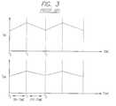
- FIGS. 3 ( a )-( b )are graphs showing current waveforms in the coupled inductors of FIG. 2 .
- FIG. 4is a schematic diagram of a converter according an embodiment of the present invention.
- FIGS. 5 ( a )-( c )are graphs showing current waveforms of currents conducting in a regulating switch and coupled inductors in the converter of FIG. 4;
- FIGS. 6 ( a )-( c )are graphs showing current waveforms of currents conducting in a regulating switch and coupled inductors where a regulation period occurs at a beginning of an off-time period of the converter of FIG. 4;
- FIG. 7is a schematic diagram of a modification of the converter of FIG. 4 where a regulation voltage is provided by the second output terminal;
- FIG. 8is a schematic diagram of a modification of the converter of FIG. 4 where a regulation voltage is provided by the first output terminal;
- FIG. 9is a schematic diagram of a converter according to another embodiment of the present invention.
- FIG. 10is a schematic diagram of a modification of the converter of FIG. 9 where a transformer has a single secondary winding.
- the present inventionprovides a DC-to-DC power converter having well-regulated dual outputs, high power density and efficiency, and which exhibits good cross-regulation.
- like element numeralsare used to describe like elements illustrated in one or more of the aforementioned figures.
- FIG. 1is a schematic diagram of a conventional converter 10 that has regulated output voltages V 01 , V 02 at output terminals 54 , 74 , respectively.
- the converter 10includes a primary side 20 and a secondary side 30 .
- On the primary side 20there is provided a power source providing input voltage V i , a primary winding 22 of a transformer 32 , a switch 24 , and a feedback control circuit 26 .
- the input voltage V iis coupled to a first end of the primary winding 22 .
- a second end of the primary winding 22is connected to the switch 24 , which in turn is connected to ground.
- the control circuit 26is connected to an activation terminal of switch 24 to control the turn on and turn off times of the switch 24 .
- the feedback control circuit 26is also connected to the output terminal 54 .
- the sections 40 and 60include secondary windings 42 , 62 of the transformer 32 , forward rectifiers 44 , 64 , freewheeling rectifiers 46 , 66 , inductors 48 , 68 , capacitors 50 , 70 , and load resistors 52 , 72 , respectively.
- the forward rectifiers 44 , 64 and freewheeling rectifiers 46 , 66are provided by diodes.
- the secondary side 30includes a switch 34 and a control circuit 36 . In the first secondary section 40 of the secondary side 30 , an anode of the forward rectifier 44 is connected to a first end of the secondary winding 42 .
- a cathode of the forward rectifier 44is connected to a cathode of the freewheeling rectifier 46 and a first end of the inductor 48 .
- a second end of the inductor 48is connected to the output terminal 54 .
- the capacitor 50 and load resistor 52also have their first ends connected to the output terminal 54 , and their second ends connected to ground.
- An anode of the freewheeling rectifier 46is also connected to ground.
- an anode of the forward rectifier 64is connected to a first end of the secondary winding 62 .
- a cathode of the forward rectifier 64is connected to a first end of switch 34 .
- a second end of switch 34is connected to a cathode of the freewheeling rectifier 66 and a first end of the inductor 68 .
- a second end of the inductor 68is connected to an output terminal 74 .
- the capacitor 70 and load resistor 72also have first ends connected to the output terminal 74 , and second ends connected to ground.
- An anode of the freewheeling rectifier 66is also connected to ground.
- the second section 60also includes a control circuit 36 that has an output terminal connected to an activation terminal of the switch 34 and an input terminal connected to the output terminal 74 .
- the second output voltage V 02is regulated by the switch 34 and control circuit 36 . Because the switch 34 is connected in series with the forward rectifier 64 , the regulation of the second output voltage V 02 occurs during the on-time of the converter 10 , which corresponds to an on-state of the switch 24 . In other words, the switch 34 further regulates the on-time of the second secondary section 60 in order to regulate the output voltage V 02 . For example, if the switch 34 is conducting for all of the on-time of the converter 10 and the voltage V 02 that is output is 5 volts, then by adjusting the on-time of the switch 34 with the control circuit 36 , the voltage V 02 can be decreased.
- switch 34is turned on for 80% of the on-time of the converter 10 , then the. output voltage V 02 is reduced to 4 volts.
- the switch 34 and the control circuit 36act as a leading-edge or a trailing-edge post-regulator.
- a disadvantage of the conventional converter 10is that the regulation of the output voltage V 02 requires conduction of the regulating switch 34 during most of the on-time of the converter 10 .
- the conventional converter 10can only step down the output voltage V 02 from its unregulated voltage level, so higher amplitude of the on-time voltage from the winding 62 is required. Therefore, rectifiers 60 , 66 and switch 34 should be designed to withstand higher voltage stress, which further increases their power losses.
- control circuit 26reduces on-time significantly under load transient conditions, the output voltage V 02 may sag downward. Accordingly, the conventional converter 10 suffers from high loss and low efficiency, as well as poor cross-regulation during transient conditions.
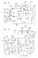
- FIG. 2is schematic diagram of a second conventional converter 12 having a regulated output voltage V 01 at output terminal 54 and a quasi-regulated output voltage V 02 at output terminal 74 .
- the converter 12includes a primary side 20 and a secondary side 80 .
- the primary side 20 of FIG. 2has the same configuration as the primary side 20 of FIG. 1 .
- On the secondary side 80there is provided essentially the same configuration as the secondary side 30 of FIG. 1, except that inductors 82 and 84 share a common core. Additionally, the switch 34 and the control circuit 36 are eliminated so that the cathode of the forward rectifier 64 is connected to the cathode of the freewheeling rectifier 66 and a first end of the inductor 84 .
- the initial voltage of the quasi-regulated output voltage V 02is determined by the regulated voltage at the first output terminal 54 and the turns ratio N 2 /N 1 of the secondary windings 64 , 44 of the transformer 32 .
- the same turns ratiowould ordinarily be utilized for the coupled inductor windings 82 , 84 to avoid high circulating currents. This puts severe limitations on the achievable voltages at the second output terminal 74 , particularly at low voltages and high currents where a high number of turns is necessary to maintain the output voltage V 02 , which further leads to high copper losses at high currents.
- FIGS. 3 ( a )- 3 ( b )are graphs showing the current waveforms of currents I 82 , I 84 flowing in the respective coupled inductors 82 , 84 .
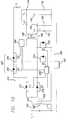
- FIG. 4is a schematic diagram of a power converter according to an embodiment of the present invention.
- the converterincludes a primary side 120 and a secondary side 130 .
- On the primary side 120there is a power source providing an input voltage V i , a primary winding 122 of a transformer 132 , a switch 124 , and a feedback control circuit 126 .
- On the secondary side 130there is provided two secondary sections 140 , 160 .
- the secondary sections 140 , 160include secondary windings 142 , 162 of the transformer 132 , forward rectifiers 144 , 164 , freewheeling rectifiers 146 , 166 , inductors 148 , 168 , capacitors 150 , 170 , and load resistors 152 , 172 , respectively. Further, the secondary side 130 includes a switch 134 and a control circuit 136 .
- the input voltage V iis coupled to a first end of the primary winding 122 .
- a second end of the primary winding 122is connected to the switch 124 , which in turn is connected to ground.
- the control circuit 126is connected to the activation terminal of the switch 124 to control the turn on and turn off times of the switch 124 .
- the control circuit 126is also connected to the output terminal 154 .
- an anode of the forward rectifier 144is connected to a first end of the secondary winding 142 .
- a cathode of the forward rectifier 144is connected to a cathode of the freewheeling rectifier 146 and a first end of the inductor 148 .
- a second end of the inductor 148is connected to an output terminal 154 .
- the capacitor 150 and load resistor 152also have their first ends connected to the output terminal 154 , and their second ends connected to ground.
- An anode of the freewheeling rectifier 146is also connected to ground.
- an anode of the forward rectifier 164is connected to a first end of the secondary winding 162 .
- a cathode of the forward rectifier 164is connected to a cathode of the freewheeling rectifier 166 and a first end of the inductor 168 .
- a second end of the inductor 168is connected to an output terminal 174 .
- the capacitor 170 and load resistor 172also have their first ends connected to the output terminal 174 , and their second ends connected to ground.
- An anode of the freewheeling rectifier 166is also connected to ground.
- the second section 160also includes the switch 134 with its first end connected to the cathode of the forward rectifier 164 and its second end connected to an auxiliary voltage source V c .
- An output of the control circuit 136is connected to an activation terminal of the switch 134 and its input connected to the output terminal 174 .
- the inductor 148is magnetically coupled to the inductor 168 so as to share the same core.
- the turns ratio NL 2 /NL 1 of the coupled inductors 168 , 148is equal to the turns ratio N 2 /N 1 of the secondary windings 162 , 142 of the transformer 132 .
- the construction of the coupled inductorsshould provide high enough leakage inductance between the inductors 148 , 168 . It should also be appreciated that the inductors 148 , 168 can also be independent from each other without magnetic coupling.
- FIGS. 5 ( a )-( b )are graphs showing the current waveforms I 148 , I 168 in the coupled inductors 148 , 168 , respectively, and FIG. 5 ( c ) is a graph showing the current waveform I reg in the regulating switch 134 .
- the input voltage V iis applied to the primary winding 122 of the transformer 132 .
- the voltages that are induced on the secondary windings 142 , 162forward bias the forward rectifiers 144 , 164 so that they become conducting.
- the voltages on the secondary windings 142 , 162are then applied to the coupled inductors 148 , 168 at the start of the on-time period.
- the current I 148 , I 168 of the coupled inductors 148 , 168is increasing as well as the magnetizing current of the coupled inductor.
- the current I 148 , I 168 of the windings 148 , 168flow into respective capacitors 150 , 170 , and into load resistors 152 , 172 , respectively.
- the switch 134is not conducting and the operation of the converter 110 is otherwise the same as the conventional converter 12 of FIG. 2 .
- the polarity on the secondary windings 142 , 162becomes reversed.
- Forward rectifiers 144 , 164turn off and freewheeling rectifiers 146 , 166 begin to conduct.
- the operation of the converter 110is the same as the converter 12 of FIG. 2; however, in a second portion of the off-time period, referred to as the regulation period T reg , the converter 110 operates differently from the conventional converter 12 .
- the control circuit 136turns on the switch 134 so that it becomes conducting.
- the auxiliary voltage Vcis applied to the inductor 168 .
- current I 148will keep decreasing at the same rate as during the off-time interval. This behavior is different from the operation of the conventional converter 12 . Referring back to FIG. 3, the current I 168 in the coupled inductor 168 does not increase during any portion of the off-time period but only decreases.
- the rate of change in the current I 148 , I 168 in the inductors 148 , 168is governed primarily by the leakage inductances associated with the windings 148 , 168 and the voltages V c , V 01 , V 02 that are applied to the respective windings of the inductors 148 , 168 .
- the rate of change in current I 168is greater than the rate of change in current I 148 . This occurs because the voltage level of V 02 is higher than the voltage level of voltage V 01 during this time.
- the ripple in the currents I 148 , I 168there is preferably provided sufficient leakage inductances between the windings of the inductors 148 , 168 .
- the leakage inductancesare too low, then the ripple in the currents I 148 , I 168 would be too high so that other parameters of the converter 110 may suffer.
- the regulation interval T regends at the beginning of the on-time period of the next duty cycle and the switch 134 is turned off.
- the voltages applied to the windings of the coupled inductors 148 , 168are essentially balanced during the on-time period, as well as during the portion of the off-time period when the second output voltage V 02 is not regulated. So, the magnetizing current redistributes between the windings of the coupled inductors 148 , 168 according to the respective last values of the currents I 148 , I 168 .
- the new value s of the leakage inductance current rates I 148 , I 168are supported by new values of the output voltages V 01 , V 02 , respectively, (e.g., higher V 02 and lower V 01 ), and changes to the duration of the regulating interval T reg allows for regulation of V 02 while V 01 is regulated by the feedback control circuit 126 .
- the application of auxiliary voltage V c for some period of time T regchanges the balance of volt-seconds applied to the three-inductor system comprising two leakage inducances of windings 148 , 168 and magnetizing inductance of the coupled inductor. The new balance of volt-seconds is then found with a different value of V 02 .
- duration of T regis decreased for higher values of the auxiliary voltage V c so that the voltage level of V c determines the power dissipation in the switch 134 .
- the pulse of current I regis short in comparison to the period of the switching frequency so that the energy dissipated in switch 134 is low.
- the freewheeling rectifier 166is not conducting so that the dissipation in the switch 134 is mostly compensated.
- FIGS. 6 ( a )-( c )are graphs showing the current waveforms in the regulating switch and the coupled inductors when the regulation period T reg occurs at the beginning of the off-time period. As illustrated in FIG. 6 ( a ), the regulation period T reg can be varied so that it occurs within any portion of the off-time interval T 1 to T 2 .
- FIG. 7is a modification of the converter of FIG. 4 that uses the second output voltage V 02 as the regulating voltage source.
- the second end of switch 134is connected to the second output terminal 174 .
- the inductor 168is shorted.
- the current flowing in the capacitor 170is redistributed to the switch 134 .
- the operation of the converter 112is essentially the same as the converter 110 , except that there is lower rate of change in the current I 168 , and a longer regulation period T reg since output voltage V 02 is normally at a lower voltage level than a voltage source providing voltage V c .
- An advantage of the converter 112is that less space and components are required as compared to the converter 110 .
- FIG. 8is another modification of the converter of FIG. 4 that uses the first output voltage V 01 as the regulating voltage.
- the second end of switch 134is connected to the first output terminal 154 .
- the current flowing in the capacitor 150is redistributed to the switch 134 .
- the operation of the converter 114is essentially the same as the converter 110 , except that there is lower rate of change in the current I 148 , and a longer regulation period T reg since output voltage V 01 is normally at a lower voltage level than a voltage source providing voltage V c .
- the converter 114requires less space and components as compared to the converter 110 . Accordingly, in the present invention, a separate voltage source providing voltage V c or any of the output voltages V 01 or V 02 can be used as the regulating voltage.
- FIG. 9is a schematic diagram of a converter according to another embodiment of the present invention.
- the rectifiers 212 , 214 , 216 , and 218are implemented as synchronous rectifiers such as MOSFETs having respective body diodes.
- a switch 220is configured in a series connection of two N-channel MOSFETs 202 , 204 having commonly coupled drain terminals. The series connection of the MOSFETs 202 , 204 prevents parasitic conduction through their respective body diodes.
- an additional control circuit 208for controlling the turn-on and turn-off times of the synchronous rectifiers 212 , 214 , 216 , and 218 .
- the forward rectifiers 216 , 212are arranged so as to be in the return path of respective sections 240 , 260 .
- the operation of the converter 210 with synchronous rectifiers 212 , 214 , 216 , and 218is the same as described above for the converter 110 of FIG. 4, except that the control circuit 208 turns off the rectifier 214 prior to turning on of the switch 220 by the control circuit 206 .
- FIG. 10is a schematic diagram of a modification of the converter of FIG. 9 where a transformer has a single secondary winding. If the turns ratio N 2 /N 1 of the secondary windings of the transformer 132 of FIG. 9 is equal to one, then a transformer 332 having one secondary winding 342 may be used as shown in FIG. 10 .
- the synchronous rectifiers 212 and 216are provided between the secondary winding 332 and the inductors 168 , 148 , respectively, whereas in FIG. 9, the rectifiers 212 , 216 are provided at the return path of the respective secondary sections of converter 210 .
- Advantages of having one secondary winding 342include simpler transformer construction and improved cross-regulation of the two output voltages V 01 , V 02 .
- the feedback control circuit 126controls load regulation for both output voltages V 01 and V 02 . Accordingly, the control circuit 206 regulates the output voltage V 02 only to the required output voltage level, which leads to a shorter regulating interval T reg , and consequently lower power dissipation.
Landscapes
- Engineering & Computer Science (AREA)
- Power Engineering (AREA)
- Dc-Dc Converters (AREA)
Abstract
Description
Claims (20)
Priority Applications (6)
| Application Number | Priority Date | Filing Date | Title |
|---|---|---|---|
| US09/948,456US6501193B1 (en) | 2001-09-07 | 2001-09-07 | Power converter having regulated dual outputs |
| AU2002332930AAU2002332930A1 (en) | 2001-09-07 | 2002-09-06 | Power converter having regulated dual outputs |
| JP2003527874AJP2005503099A (en) | 2001-09-07 | 2002-09-06 | Power converter with two regulated outputs |
| EP02798168AEP1423906A2 (en) | 2001-09-07 | 2002-09-06 | Power converter having regulated dual outputs |
| PCT/US2002/028583WO2003023945A2 (en) | 2001-09-07 | 2002-09-06 | Power converter having regulated dual outputs |
| CNA028173678ACN1552120A (en) | 2001-09-07 | 2002-09-06 | Power converter having stable dual outputs |
Applications Claiming Priority (1)
| Application Number | Priority Date | Filing Date | Title |
|---|---|---|---|
| US09/948,456US6501193B1 (en) | 2001-09-07 | 2001-09-07 | Power converter having regulated dual outputs |
Publications (1)
| Publication Number | Publication Date |
|---|---|
| US6501193B1true US6501193B1 (en) | 2002-12-31 |
Family
ID=25487871
Family Applications (1)
| Application Number | Title | Priority Date | Filing Date |
|---|---|---|---|
| US09/948,456Expired - LifetimeUS6501193B1 (en) | 2001-09-07 | 2001-09-07 | Power converter having regulated dual outputs |
Country Status (6)
| Country | Link |
|---|---|
| US (1) | US6501193B1 (en) |
| EP (1) | EP1423906A2 (en) |
| JP (1) | JP2005503099A (en) |
| CN (1) | CN1552120A (en) |
| AU (1) | AU2002332930A1 (en) |
| WO (1) | WO2003023945A2 (en) |
Cited By (47)
| Publication number | Priority date | Publication date | Assignee | Title |
|---|---|---|---|---|
| US20020187675A1 (en)* | 2001-05-09 | 2002-12-12 | Mcmullin Faris W. | Integrated cord take-up assembly |
| US6775159B2 (en)* | 2001-02-19 | 2004-08-10 | Rockwell Scientific Company, Llc. | Switching power converter circuits providing main and auxiliary output voltages |
| US20050243481A1 (en)* | 2004-04-30 | 2005-11-03 | Williams David A | Primary side turn-off of self-driven synchronous rectifiers |
| US20070069581A1 (en)* | 2005-09-29 | 2007-03-29 | Fuji Electric Device Technology Co., Ltd. | AC to DC converter circuit |
| US20070138870A1 (en)* | 2005-12-21 | 2007-06-21 | Sanken Electric Co., Ltd. | Multi-output switching power supply |
| US7280026B2 (en) | 2002-04-18 | 2007-10-09 | Coldwatt, Inc. | Extended E matrix integrated magnetics (MIM) core |
| US7298118B2 (en) | 2005-02-23 | 2007-11-20 | Coldwatt, Inc. | Power converter employing a tapped inductor and integrated magnetics and method of operating the same |
| US7321283B2 (en) | 2004-08-19 | 2008-01-22 | Coldwatt, Inc. | Vertical winding structures for planar magnetic switched-mode power converters |
| US7385375B2 (en) | 2005-02-23 | 2008-06-10 | Coldwatt, Inc. | Control circuit for a depletion mode switch and method of operating the same |
| US7417875B2 (en) | 2005-02-08 | 2008-08-26 | Coldwatt, Inc. | Power converter employing integrated magnetics with a current multiplier rectifier and method of operating the same |
| US7427910B2 (en) | 2004-08-19 | 2008-09-23 | Coldwatt, Inc. | Winding structure for efficient switch-mode power converters |
| US7667986B2 (en) | 2006-12-01 | 2010-02-23 | Flextronics International Usa, Inc. | Power system with power converters having an adaptive controller |
| US7675759B2 (en) | 2006-12-01 | 2010-03-09 | Flextronics International Usa, Inc. | Power system with power converters having an adaptive controller |
| US7675758B2 (en) | 2006-12-01 | 2010-03-09 | Flextronics International Usa, Inc. | Power converter with an adaptive controller and method of operating the same |
| US7876191B2 (en) | 2005-02-23 | 2011-01-25 | Flextronics International Usa, Inc. | Power converter employing a tapped inductor and integrated magnetics and method of operating the same |
| US7889517B2 (en) | 2006-12-01 | 2011-02-15 | Flextronics International Usa, Inc. | Power system with power converters having an adaptive controller |
| US7906941B2 (en) | 2007-06-19 | 2011-03-15 | Flextronics International Usa, Inc. | System and method for estimating input power for a power processing circuit |
| US8068355B1 (en)* | 2005-02-17 | 2011-11-29 | Volterra Semiconductor Corporation | Apparatus for isolated switching power supply with coupled output inductors |
| US8125205B2 (en) | 2006-08-31 | 2012-02-28 | Flextronics International Usa, Inc. | Power converter employing regulators with a coupled inductor |
| CN101286706B (en)* | 2007-02-13 | 2013-04-24 | 伊斯帕诺-絮扎公司 | Unipolar or bipolar chopping converter with three magnetically coupled windings |
| US8502520B2 (en) | 2007-03-14 | 2013-08-06 | Flextronics International Usa, Inc | Isolated power converter |
| US8514593B2 (en) | 2009-06-17 | 2013-08-20 | Power Systems Technologies, Ltd. | Power converter employing a variable switching frequency and a magnetic device with a non-uniform gap |
| US8520414B2 (en) | 2009-01-19 | 2013-08-27 | Power Systems Technologies, Ltd. | Controller for a power converter |
| US8520420B2 (en) | 2009-12-18 | 2013-08-27 | Power Systems Technologies, Ltd. | Controller for modifying dead time between switches in a power converter |
| US8638578B2 (en) | 2009-08-14 | 2014-01-28 | Power System Technologies, Ltd. | Power converter including a charge pump employable in a power adapter |
| US8643222B2 (en) | 2009-06-17 | 2014-02-04 | Power Systems Technologies Ltd | Power adapter employing a power reducer |
| US8767418B2 (en) | 2010-03-17 | 2014-07-01 | Power Systems Technologies Ltd. | Control system for a power converter and method of operating the same |
| US8787043B2 (en) | 2010-01-22 | 2014-07-22 | Power Systems Technologies, Ltd. | Controller for a power converter and method of operating the same |
| US8792256B2 (en) | 2012-01-27 | 2014-07-29 | Power Systems Technologies Ltd. | Controller for a switch and method of operating the same |
| US8792257B2 (en) | 2011-03-25 | 2014-07-29 | Power Systems Technologies, Ltd. | Power converter with reduced power dissipation |
| US8976549B2 (en) | 2009-12-03 | 2015-03-10 | Power Systems Technologies, Ltd. | Startup circuit including first and second Schmitt triggers and power converter employing the same |
| US9019061B2 (en) | 2009-03-31 | 2015-04-28 | Power Systems Technologies, Ltd. | Magnetic device formed with U-shaped core pieces and power converter employing the same |
| US9077248B2 (en) | 2009-06-17 | 2015-07-07 | Power Systems Technologies Ltd | Start-up circuit for a power adapter |
| US9088216B2 (en) | 2009-01-19 | 2015-07-21 | Power Systems Technologies, Ltd. | Controller for a synchronous rectifier switch |
| US9099232B2 (en) | 2012-07-16 | 2015-08-04 | Power Systems Technologies Ltd. | Magnetic device and power converter employing the same |
| US9106130B2 (en) | 2012-07-16 | 2015-08-11 | Power Systems Technologies, Inc. | Magnetic device and power converter employing the same |
| US9190898B2 (en) | 2012-07-06 | 2015-11-17 | Power Systems Technologies, Ltd | Controller for a power converter and method of operating the same |
| US9197132B2 (en) | 2006-12-01 | 2015-11-24 | Flextronics International Usa, Inc. | Power converter with an adaptive controller and method of operating the same |
| US9214264B2 (en) | 2012-07-16 | 2015-12-15 | Power Systems Technologies, Ltd. | Magnetic device and power converter employing the same |
| US9240712B2 (en) | 2012-12-13 | 2016-01-19 | Power Systems Technologies Ltd. | Controller including a common current-sense device for power switches of a power converter |
| US9246391B2 (en) | 2010-01-22 | 2016-01-26 | Power Systems Technologies Ltd. | Controller for providing a corrected signal to a sensed peak current through a circuit element of a power converter |
| US9300206B2 (en) | 2013-11-15 | 2016-03-29 | Power Systems Technologies Ltd. | Method for estimating power of a power converter |
| US9379629B2 (en) | 2012-07-16 | 2016-06-28 | Power Systems Technologies, Ltd. | Magnetic device and power converter employing the same |
| US9691538B1 (en) | 2012-08-30 | 2017-06-27 | Volterra Semiconductor LLC | Magnetic devices for power converters with light load enhancers |
| US10811984B2 (en) | 2015-04-24 | 2020-10-20 | Schmidhauser Ag | Bidirectional DC-to-DC converter with voltage limitation device including switching element and voltage limitation capacitor |
| US11552572B2 (en) | 2020-02-13 | 2023-01-10 | Hamilton Sundstrand Corporation | Critical load management in secondary winding in auxiliary power supply |
| US20230318471A1 (en)* | 2022-03-30 | 2023-10-05 | Infineon Technologies Austria Ag | Circuit for bi-directional converter, bi-directional converter and operation method thereof |
Families Citing this family (10)
| Publication number | Priority date | Publication date | Assignee | Title |
|---|---|---|---|---|
| US7564229B2 (en)* | 2006-03-01 | 2009-07-21 | Power Integrations, Inc. | Method and apparatus for power conversion and regulation in a power converter having a plurality of outputs |
| US20080062725A1 (en)* | 2006-09-11 | 2008-03-13 | Ta-Yung Yang | Multi-channels power converter having power saving means to improve light load efficiency |
| CN101211191B (en)* | 2006-12-25 | 2010-04-14 | 艾默生网络能源系统有限公司 | Directional regulating circuit |
| FR2912566B1 (en)* | 2007-02-13 | 2009-05-01 | Hispano Suiza Sa | UNIPOLAR OR BIPOLAR CUTTING CONVERTER WITH TWO MAGNETICALLY COUPLED WINDINGS. |
| WO2008146314A1 (en)* | 2007-05-30 | 2008-12-04 | Power-One Italy S.P.A. | Multi-output synchronous flyback converter |
| US9071152B2 (en)* | 2012-07-03 | 2015-06-30 | Cognipower, Llc | Power converter with demand pulse isolation |
| JP6143951B2 (en)* | 2013-09-19 | 2017-06-07 | フィリップス ライティング ホールディング ビー ヴィ | Compact driver with integrated dual output, especially for light emitting diodes |
| CN105576956B (en)* | 2014-11-05 | 2019-11-19 | 中兴通讯股份有限公司 | Power circuit and Switching Power Supply |
| CN110289768B (en)* | 2019-07-26 | 2021-04-20 | 北京机械设备研究所 | Cross regulation rate control circuit and method for multi-output power supply |
| CN115021575A (en)* | 2022-06-14 | 2022-09-06 | 苏州时代新安能源科技有限公司 | Cross-Regulation Circuits and Power Systems |
Citations (10)
| Publication number | Priority date | Publication date | Assignee | Title |
|---|---|---|---|---|
| US4302803A (en)* | 1980-01-16 | 1981-11-24 | Sperry Corporation | Rectifier-converter power supply with multi-channel flyback inverter |
| US4660136A (en)* | 1985-01-24 | 1987-04-21 | Honeywell Inc. | Single regulation power supply with load compensation of an auxiliary voltage output |
| US4672516A (en)* | 1985-02-25 | 1987-06-09 | Siemens Aktiengesellschaft | Primary side clock single-ended forward converter with connectible secondary circuits and having switchable actual value feed for the output voltage control |
| US4703409A (en)* | 1983-09-26 | 1987-10-27 | International Business Machines Corporation | Coupled power supply inductors for reduced ripple current |
| US5008794A (en)* | 1989-12-21 | 1991-04-16 | Power Integrations, Inc. | Regulated flyback converter with spike suppressing coupled inductors |
| US5363323A (en)* | 1993-08-11 | 1994-11-08 | International Business Machines Corporation | Power supply with plural outputs supplying dynamic and steady loads |
| US5612862A (en)* | 1994-05-06 | 1997-03-18 | Alcatel Network Systems, Inc. | Method and circuitry for controlling current reset characteristics of a magnetic amplifier control circuit |
| US5715153A (en) | 1996-12-11 | 1998-02-03 | International Power Devices, Inc. | Dual-output DC-DC power supply |
| US5886508A (en) | 1997-08-29 | 1999-03-23 | Computer Products, Inc. | Multiple output voltages from a cascaded buck converter topology |
| US6212081B1 (en)* | 1999-05-14 | 2001-04-03 | Nihon Protector Co., Ltd. | Uninterruptible duplexed power supply system |
Family Cites Families (23)
| Publication number | Priority date | Publication date | Assignee | Title |
|---|---|---|---|---|
| JPS5465324A (en)* | 1977-11-02 | 1979-05-25 | Hirobumi Matsuo | Multiple output direct current power converter |
| JPS5568880A (en)* | 1978-11-20 | 1980-05-23 | Tdk Corp | Multi-output switching regulator |
| SU875361A1 (en)* | 1980-01-21 | 1981-10-23 | Чувашский государственный университет им. И.Н.Ульянова | Pulsed stabilizer |
| JPS56139075A (en)* | 1980-03-31 | 1981-10-30 | Kosuke Harada | High accuracy multioutput forward dc/dc converter |
| JPS5725169A (en)* | 1980-07-18 | 1982-02-09 | Fujitsu Ltd | Dc/dc converter |
| JPS5788876A (en)* | 1980-11-21 | 1982-06-02 | Fujitsu Ltd | Dc/dc converter |
| FR2529698B1 (en)* | 1982-07-02 | 1985-09-13 | Radiotechnique Compelec | STABILIZED OUTPUT SUPPLY CIRCUIT AND APPLICATION TO MULTI-VOLTAGE SUPPLY |
| JPS6074965A (en)* | 1983-09-30 | 1985-04-27 | Hitachi Ltd | Multioutput switching power source |
| US4581690A (en)* | 1984-03-15 | 1986-04-08 | Zenith Corporation | Switched-mode power supply with output post-regulator |
| JPS61185069A (en)* | 1985-02-12 | 1986-08-18 | Hitachi Metals Ltd | Dc/dc converter |
| JPH0245433B2 (en)* | 1985-08-29 | 1990-10-09 | Pfu Ltd | DCCDCKONBAATANOJIKIANPUSEIGYOSOCHI |
| JPH0260465A (en)* | 1988-08-26 | 1990-02-28 | Hitachi Lighting Ltd | Dc stabilized power source |
| DE3940955A1 (en)* | 1988-12-29 | 1990-08-16 | Ceag Licht & Strom | Switched power supply - has coupled converter stages to provide different voltage levels |
| US5113333A (en)* | 1990-01-08 | 1992-05-12 | Intech, Inc. | Magnetic DC-to-DC converter |
| US5075839A (en)* | 1990-04-05 | 1991-12-24 | General Electric Company | Inductor shunt, output voltage regulation system for a power supply |
| JP3324096B2 (en)* | 1991-07-03 | 2002-09-17 | 横河電機株式会社 | Multi-output DC power supply using cross regulation choke coil |
| US5479087A (en)* | 1992-10-02 | 1995-12-26 | Compaq Computer Corp. | Synchronized switch tapped coupled inductor regulation circuit |
| US5363287A (en)* | 1994-03-01 | 1994-11-08 | Philips Electronics North America Corporation | Low noise multi-output and multi-resonant forward converter for television power supplies |
| DE19530064A1 (en)* | 1995-08-16 | 1997-02-20 | Bosch Gmbh Robert | Controlled converter with at least two secondary circuits |
| JPH11220886A (en)* | 1997-11-25 | 1999-08-10 | Denso Corp | Multilevel-type power converter |
| US6351403B2 (en)* | 1998-09-25 | 2002-02-26 | International Rectifier Corp. | Secondary side switching regulator having a phase lock loop control circuit |
| US6058026A (en)* | 1999-07-26 | 2000-05-02 | Lucent Technologies, Inc. | Multiple output converter having a single transformer winding and independent output regulation |
| DE69939535D1 (en)* | 1999-08-20 | 2008-10-23 | Em Microelectronic Marin Sa | System for controlling a bi-directional switch with two transistors |
- 2001
- 2001-09-07USUS09/948,456patent/US6501193B1/ennot_activeExpired - Lifetime
- 2002
- 2002-09-06CNCNA028173678Apatent/CN1552120A/enactivePending
- 2002-09-06JPJP2003527874Apatent/JP2005503099A/enactivePending
- 2002-09-06EPEP02798168Apatent/EP1423906A2/ennot_activeWithdrawn
- 2002-09-06AUAU2002332930Apatent/AU2002332930A1/ennot_activeAbandoned
- 2002-09-06WOPCT/US2002/028583patent/WO2003023945A2/ennot_activeApplication Discontinuation
Patent Citations (10)
| Publication number | Priority date | Publication date | Assignee | Title |
|---|---|---|---|---|
| US4302803A (en)* | 1980-01-16 | 1981-11-24 | Sperry Corporation | Rectifier-converter power supply with multi-channel flyback inverter |
| US4703409A (en)* | 1983-09-26 | 1987-10-27 | International Business Machines Corporation | Coupled power supply inductors for reduced ripple current |
| US4660136A (en)* | 1985-01-24 | 1987-04-21 | Honeywell Inc. | Single regulation power supply with load compensation of an auxiliary voltage output |
| US4672516A (en)* | 1985-02-25 | 1987-06-09 | Siemens Aktiengesellschaft | Primary side clock single-ended forward converter with connectible secondary circuits and having switchable actual value feed for the output voltage control |
| US5008794A (en)* | 1989-12-21 | 1991-04-16 | Power Integrations, Inc. | Regulated flyback converter with spike suppressing coupled inductors |
| US5363323A (en)* | 1993-08-11 | 1994-11-08 | International Business Machines Corporation | Power supply with plural outputs supplying dynamic and steady loads |
| US5612862A (en)* | 1994-05-06 | 1997-03-18 | Alcatel Network Systems, Inc. | Method and circuitry for controlling current reset characteristics of a magnetic amplifier control circuit |
| US5715153A (en) | 1996-12-11 | 1998-02-03 | International Power Devices, Inc. | Dual-output DC-DC power supply |
| US5886508A (en) | 1997-08-29 | 1999-03-23 | Computer Products, Inc. | Multiple output voltages from a cascaded buck converter topology |
| US6212081B1 (en)* | 1999-05-14 | 2001-04-03 | Nihon Protector Co., Ltd. | Uninterruptible duplexed power supply system |
Cited By (60)
| Publication number | Priority date | Publication date | Assignee | Title |
|---|---|---|---|---|
| US6775159B2 (en)* | 2001-02-19 | 2004-08-10 | Rockwell Scientific Company, Llc. | Switching power converter circuits providing main and auxiliary output voltages |
| US20020187675A1 (en)* | 2001-05-09 | 2002-12-12 | Mcmullin Faris W. | Integrated cord take-up assembly |
| US8134443B2 (en) | 2002-04-18 | 2012-03-13 | Flextronics International Usa, Inc. | Extended E matrix integrated magnetics (MIM) core |
| US7633369B2 (en) | 2002-04-18 | 2009-12-15 | Flextronics International Usa, Inc. | Extended E matrix integrated magnetics (MIM) core |
| US7280026B2 (en) | 2002-04-18 | 2007-10-09 | Coldwatt, Inc. | Extended E matrix integrated magnetics (MIM) core |
| US7333350B2 (en) | 2004-04-30 | 2008-02-19 | Power One, Inc. | Self driven synchronous rectifier shutdown circuit and method |
| US20050243481A1 (en)* | 2004-04-30 | 2005-11-03 | Williams David A | Primary side turn-off of self-driven synchronous rectifiers |
| US7203041B2 (en) | 2004-04-30 | 2007-04-10 | Power-One, Inc | Primary side turn-off of self-driven synchronous rectifiers |
| US20070103819A1 (en)* | 2004-04-30 | 2007-05-10 | Williams David A | Self Driven Synchronous Rectifier Shutdown Circuit and Method |
| US7554430B2 (en) | 2004-08-19 | 2009-06-30 | Flextronics International Usa, Inc. | Vertical winding structures for planar magnetic switched-mode power converters |
| US7427910B2 (en) | 2004-08-19 | 2008-09-23 | Coldwatt, Inc. | Winding structure for efficient switch-mode power converters |
| US7321283B2 (en) | 2004-08-19 | 2008-01-22 | Coldwatt, Inc. | Vertical winding structures for planar magnetic switched-mode power converters |
| US7417875B2 (en) | 2005-02-08 | 2008-08-26 | Coldwatt, Inc. | Power converter employing integrated magnetics with a current multiplier rectifier and method of operating the same |
| US7675764B2 (en) | 2005-02-08 | 2010-03-09 | Flextronics International Usa, Inc. | Power converter employing integrated magnetics with a current multiplier rectifier and method of operating the same |
| US8068355B1 (en)* | 2005-02-17 | 2011-11-29 | Volterra Semiconductor Corporation | Apparatus for isolated switching power supply with coupled output inductors |
| US7385375B2 (en) | 2005-02-23 | 2008-06-10 | Coldwatt, Inc. | Control circuit for a depletion mode switch and method of operating the same |
| US7298118B2 (en) | 2005-02-23 | 2007-11-20 | Coldwatt, Inc. | Power converter employing a tapped inductor and integrated magnetics and method of operating the same |
| US7876191B2 (en) | 2005-02-23 | 2011-01-25 | Flextronics International Usa, Inc. | Power converter employing a tapped inductor and integrated magnetics and method of operating the same |
| US7679213B2 (en)* | 2005-09-29 | 2010-03-16 | Fuji Electric Device Technology Co., Ltd. | AC to DC converter circuit |
| US20070069581A1 (en)* | 2005-09-29 | 2007-03-29 | Fuji Electric Device Technology Co., Ltd. | AC to DC converter circuit |
| US7629781B2 (en)* | 2005-12-21 | 2009-12-08 | Sanken Electric Co., Ltd. | Multi-output switching power supply |
| US20070138870A1 (en)* | 2005-12-21 | 2007-06-21 | Sanken Electric Co., Ltd. | Multi-output switching power supply |
| US8125205B2 (en) | 2006-08-31 | 2012-02-28 | Flextronics International Usa, Inc. | Power converter employing regulators with a coupled inductor |
| US7675758B2 (en) | 2006-12-01 | 2010-03-09 | Flextronics International Usa, Inc. | Power converter with an adaptive controller and method of operating the same |
| US7675759B2 (en) | 2006-12-01 | 2010-03-09 | Flextronics International Usa, Inc. | Power system with power converters having an adaptive controller |
| US7889517B2 (en) | 2006-12-01 | 2011-02-15 | Flextronics International Usa, Inc. | Power system with power converters having an adaptive controller |
| US9197132B2 (en) | 2006-12-01 | 2015-11-24 | Flextronics International Usa, Inc. | Power converter with an adaptive controller and method of operating the same |
| US7667986B2 (en) | 2006-12-01 | 2010-02-23 | Flextronics International Usa, Inc. | Power system with power converters having an adaptive controller |
| US8477514B2 (en) | 2006-12-01 | 2013-07-02 | Flextronics International Usa, Inc. | Power system with power converters having an adaptive controller |
| CN101286706B (en)* | 2007-02-13 | 2013-04-24 | 伊斯帕诺-絮扎公司 | Unipolar or bipolar chopping converter with three magnetically coupled windings |
| US8502520B2 (en) | 2007-03-14 | 2013-08-06 | Flextronics International Usa, Inc | Isolated power converter |
| US7906941B2 (en) | 2007-06-19 | 2011-03-15 | Flextronics International Usa, Inc. | System and method for estimating input power for a power processing circuit |
| US8520414B2 (en) | 2009-01-19 | 2013-08-27 | Power Systems Technologies, Ltd. | Controller for a power converter |
| US9088216B2 (en) | 2009-01-19 | 2015-07-21 | Power Systems Technologies, Ltd. | Controller for a synchronous rectifier switch |
| US9019061B2 (en) | 2009-03-31 | 2015-04-28 | Power Systems Technologies, Ltd. | Magnetic device formed with U-shaped core pieces and power converter employing the same |
| US8643222B2 (en) | 2009-06-17 | 2014-02-04 | Power Systems Technologies Ltd | Power adapter employing a power reducer |
| US9077248B2 (en) | 2009-06-17 | 2015-07-07 | Power Systems Technologies Ltd | Start-up circuit for a power adapter |
| US8514593B2 (en) | 2009-06-17 | 2013-08-20 | Power Systems Technologies, Ltd. | Power converter employing a variable switching frequency and a magnetic device with a non-uniform gap |
| US8638578B2 (en) | 2009-08-14 | 2014-01-28 | Power System Technologies, Ltd. | Power converter including a charge pump employable in a power adapter |
| US8976549B2 (en) | 2009-12-03 | 2015-03-10 | Power Systems Technologies, Ltd. | Startup circuit including first and second Schmitt triggers and power converter employing the same |
| US8520420B2 (en) | 2009-12-18 | 2013-08-27 | Power Systems Technologies, Ltd. | Controller for modifying dead time between switches in a power converter |
| US8787043B2 (en) | 2010-01-22 | 2014-07-22 | Power Systems Technologies, Ltd. | Controller for a power converter and method of operating the same |
| US9246391B2 (en) | 2010-01-22 | 2016-01-26 | Power Systems Technologies Ltd. | Controller for providing a corrected signal to a sensed peak current through a circuit element of a power converter |
| US8767418B2 (en) | 2010-03-17 | 2014-07-01 | Power Systems Technologies Ltd. | Control system for a power converter and method of operating the same |
| US8792257B2 (en) | 2011-03-25 | 2014-07-29 | Power Systems Technologies, Ltd. | Power converter with reduced power dissipation |
| US8792256B2 (en) | 2012-01-27 | 2014-07-29 | Power Systems Technologies Ltd. | Controller for a switch and method of operating the same |
| US9190898B2 (en) | 2012-07-06 | 2015-11-17 | Power Systems Technologies, Ltd | Controller for a power converter and method of operating the same |
| US9106130B2 (en) | 2012-07-16 | 2015-08-11 | Power Systems Technologies, Inc. | Magnetic device and power converter employing the same |
| US9214264B2 (en) | 2012-07-16 | 2015-12-15 | Power Systems Technologies, Ltd. | Magnetic device and power converter employing the same |
| US9099232B2 (en) | 2012-07-16 | 2015-08-04 | Power Systems Technologies Ltd. | Magnetic device and power converter employing the same |
| US9379629B2 (en) | 2012-07-16 | 2016-06-28 | Power Systems Technologies, Ltd. | Magnetic device and power converter employing the same |
| US9691538B1 (en) | 2012-08-30 | 2017-06-27 | Volterra Semiconductor LLC | Magnetic devices for power converters with light load enhancers |
| US11062830B1 (en) | 2012-08-30 | 2021-07-13 | Volterra Semiconductor LLC | Magnetic devices for power converters with light load enhancers |
| US11862389B1 (en) | 2012-08-30 | 2024-01-02 | Volterra Semiconductor LLC | Magnetic devices for power converters with light load enhancers |
| US9240712B2 (en) | 2012-12-13 | 2016-01-19 | Power Systems Technologies Ltd. | Controller including a common current-sense device for power switches of a power converter |
| US9300206B2 (en) | 2013-11-15 | 2016-03-29 | Power Systems Technologies Ltd. | Method for estimating power of a power converter |
| US10811984B2 (en) | 2015-04-24 | 2020-10-20 | Schmidhauser Ag | Bidirectional DC-to-DC converter with voltage limitation device including switching element and voltage limitation capacitor |
| US11552572B2 (en) | 2020-02-13 | 2023-01-10 | Hamilton Sundstrand Corporation | Critical load management in secondary winding in auxiliary power supply |
| US20230318471A1 (en)* | 2022-03-30 | 2023-10-05 | Infineon Technologies Austria Ag | Circuit for bi-directional converter, bi-directional converter and operation method thereof |
| US12395089B2 (en)* | 2022-03-30 | 2025-08-19 | Infineon Technologies Austria Ag | Circuit for bi-directional converter, bi-directional converter and operation method thereof |
Also Published As
| Publication number | Publication date |
|---|---|
| JP2005503099A (en) | 2005-01-27 |
| WO2003023945A2 (en) | 2003-03-20 |
| WO2003023945A3 (en) | 2003-10-09 |
| AU2002332930A1 (en) | 2003-03-24 |
| EP1423906A2 (en) | 2004-06-02 |
| CN1552120A (en) | 2004-12-01 |
Similar Documents
| Publication | Publication Date | Title |
|---|---|---|
| US6501193B1 (en) | Power converter having regulated dual outputs | |
| US11848603B2 (en) | Auxiliary power supply apparatus and method for isolated power converters | |
| US9318967B2 (en) | DC to DC converter and DC to DC conversion system | |
| US7872879B2 (en) | Switched mode power converter and method of operation thereof | |
| US7570501B2 (en) | DC-DC converter with capacitor precharging and duty ratio limiting | |
| US7023186B2 (en) | Two stage boost converter topology | |
| US5305191A (en) | Drive circuit for zero-voltage switching power converter with controlled power switch turn-on | |
| US6831847B2 (en) | Synchronous rectifier drive circuit and power supply including same | |
| US6344768B1 (en) | Full-bridge DC-to-DC converter having an unipolar gate drive | |
| US6778412B2 (en) | Synchronous converter with reverse current protection through variable inductance | |
| EP1229635B1 (en) | Active gate clamp circuit for self driven synchronous rectifiers | |
| US6856521B1 (en) | Pulse width modulation soft-switching control | |
| JP2000152615A (en) | Power supply for using circulation capacitor and its operation method | |
| EP0966091A2 (en) | DC to DC power converter with integrated magnetic power transformer | |
| KR100874809B1 (en) | Three-Level DC-DC Converter Using Zero-Voltage-to-Current Switching | |
| US20080290730A1 (en) | Flyback Converter | |
| US7079403B2 (en) | Isolated DC-DC converters | |
| KR100842734B1 (en) | Three-Level DC-DC Converter Using Zero-Voltage-to-Current Switching | |
| US6515877B1 (en) | DC-to-DC converter providing high current and low voltage | |
| US6628533B2 (en) | DC-to-DC converter providing high current and low voltage | |
| KR20200100057A (en) | Isolated switching power supply | |
| JP7606627B2 (en) | Switching control device, switching power supply device and power supply system | |
| KR100803230B1 (en) | Synchronous rectifier circuit | |
| EP1994634B1 (en) | A power converter | |
| JPH07337034A (en) | Zero voltage switching power supply |
Legal Events
| Date | Code | Title | Description |
|---|---|---|---|
| AS | Assignment | Owner name:POWER-ONE, INC., CALIFORNIA Free format text:ASSIGNMENT OF ASSIGNORS INTEREST;ASSIGNOR:KRUGLY, SIMON;REEL/FRAME:012442/0411 Effective date:20010904 | |
| STCF | Information on status: patent grant | Free format text:PATENTED CASE | |
| RF | Reissue application filed | Effective date:20041217 | |
| FPAY | Fee payment | Year of fee payment:4 | |
| AS | Assignment | Owner name:PWER BRIDGE, LLC, ALASKA Free format text:SECURITY AGREEMENT;ASSIGNOR:POWER-ONE, INC.;REEL/FRAME:020617/0177 Effective date:20080306 Owner name:PWER BRIDGE, LLC,ALASKA Free format text:SECURITY AGREEMENT;ASSIGNOR:POWER-ONE, INC.;REEL/FRAME:020617/0177 Effective date:20080306 | |
| AS | Assignment | Owner name:PWER BRIDGE, LLC, ARKANSAS Free format text:CORRECTIV;ASSIGNOR:POWER-ONE, INC.;REEL/FRAME:020741/0403 Effective date:20080306 Owner name:PWER BRIDGE, LLC,ARKANSAS Free format text:CORRECTIVE ASSIGNMENT TO CORRECT THE ASSIGNEE ADDR;ASSIGNOR:POWER-ONE, INC.;REEL/FRAME:020741/0403 Effective date:20080306 Owner name:PWER BRIDGE, LLC, ARKANSAS Free format text:CORRECTIVE ASSIGNMENT TO CORRECT THE ASSIGNEE ADDR;ASSIGNOR:POWER-ONE, INC.;REEL/FRAME:020741/0403 Effective date:20080306 | |
| AS | Assignment | Owner name:POWER-ONE, INC., CALIFORNIA Free format text:RELEASE BY SECURED PARTY;ASSIGNOR:PWER BRIDGE, LLC;REEL/FRAME:021253/0024 Effective date:20080617 Owner name:THE BANK OF NEW YORK TRUST COMPANY, N.A., CALIFORN Free format text:SECURITY AGREEMENT;ASSIGNOR:POWER-ONE, INC.;REEL/FRAME:021253/0076 Effective date:20080617 Owner name:POWER-ONE, INC.,CALIFORNIA Free format text:RELEASE BY SECURED PARTY;ASSIGNOR:PWER BRIDGE, LLC;REEL/FRAME:021253/0024 Effective date:20080617 Owner name:THE BANK OF NEW YORK TRUST COMPANY, N.A.,CALIFORNI Free format text:SECURITY AGREEMENT;ASSIGNOR:POWER-ONE, INC.;REEL/FRAME:021253/0076 Effective date:20080617 | |
| FPAY | Fee payment | Year of fee payment:8 | |
| AS | Assignment | Owner name:POWER-ONE, INC., CALIFORNIA Free format text:RELEASE BY SECURED PARTY;ASSIGNOR:THE BANK OF NEW YORK MELLON TRUST COMPANY, N.A. (AS SUCCESSOR TO THE BANK OF NEW YORK TRUST COMPANY, N.A.);REEL/FRAME:026026/0794 Effective date:20110317 | |
| AS | Assignment | Owner name:BANK OF AMERICA, N.A., WASHINGTON Free format text:SECURITY AGREEMENT;ASSIGNOR:POWER-ONE, INC.;REEL/FRAME:026401/0098 Effective date:20110329 | |
| AS | Assignment | Owner name:POWER-ONE, INC., CALIFORNIA Free format text:RELEASE BY SECURED PARTY;ASSIGNOR:BANK OF AMERICA, N.A. AS ADMINISTRATIVE AGENT;REEL/FRAME:032826/0684 Effective date:20130722 | |
| FPAY | Fee payment | Year of fee payment:12 | |
| AS | Assignment | Owner name:PAI CAPITAL LLC, CALIFORNIA Free format text:NUNC PRO TUNC ASSIGNMENT;ASSIGNOR:POWER-ONE, INC.;REEL/FRAME:033227/0968 Effective date:20140604 | |
| AS | Assignment | Owner name:BEL POWER SOLUTIONS INC., CALIFORNIA Free format text:ASSIGNMENT OF ASSIGNORS INTEREST;ASSIGNOR:PAI CAPITAL LLC;REEL/FRAME:043086/0433 Effective date:20170615 | |
| AS | Assignment | Owner name:KEYBANK NATIONAL ASSOCIATION, AS ADMINISTRATIVE AGENT, OHIO Free format text:SECURITY INTEREST;ASSIGNOR:BEL FUSE INC.;REEL/FRAME:058917/0452 Effective date:20210902 |