US6501161B1 - Semiconductor package having increased solder joint strength - Google Patents
Semiconductor package having increased solder joint strengthDownload PDFInfo
- Publication number
- US6501161B1 US6501161B1US09/687,485US68748500AUS6501161B1US 6501161 B1US6501161 B1US 6501161B1US 68748500 AUS68748500 AUS 68748500AUS 6501161 B1US6501161 B1US 6501161B1
- Authority
- US
- United States
- Prior art keywords
- chip
- leads
- semiconductor package
- chip paddle
- paddle
- Prior art date
- Legal status (The legal status is an assumption and is not a legal conclusion. Google has not performed a legal analysis and makes no representation as to the accuracy of the status listed.)
- Expired - Lifetime
Links
- 239000004065semiconductorSubstances0.000titleclaimsabstractdescription165
- 229910000679solderInorganic materials0.000titleabstractdescription17
- 239000000463materialSubstances0.000claimsabstractdescription50
- 238000005538encapsulationMethods0.000claimsabstractdescription21
- 239000000853adhesiveSubstances0.000claimsdescription8
- 230000001070adhesive effectEffects0.000claimsdescription8
- 230000002093peripheral effectEffects0.000abstract1
- 238000000034methodMethods0.000description11
- 238000004519manufacturing processMethods0.000description5
- 239000008393encapsulating agentSubstances0.000description3
- 239000004033plasticSubstances0.000description3
- 239000011248coating agentSubstances0.000description2
- 238000000576coating methodMethods0.000description2
- 239000004020conductorSubstances0.000description2
- 238000005530etchingMethods0.000description2
- 239000004634thermosetting polymerSubstances0.000description2
- 239000004593EpoxySubstances0.000description1
- 235000019593adhesivenessNutrition0.000description1
- 230000001413cellular effectEffects0.000description1
- 238000003486chemical etchingMethods0.000description1
- 238000010276constructionMethods0.000description1
- 238000005516engineering processMethods0.000description1
- 125000003700epoxy groupChemical group0.000description1
- PCHJSUWPFVWCPO-UHFFFAOYSA-NgoldChemical compound[Au]PCHJSUWPFVWCPO-UHFFFAOYSA-N0.000description1
- 229910052737goldInorganic materials0.000description1
- 239000010931goldSubstances0.000description1
- 239000000383hazardous chemicalSubstances0.000description1
- 239000002184metalSubstances0.000description1
- 229910052751metalInorganic materials0.000description1
- 238000004377microelectronicMethods0.000description1
- 238000012986modificationMethods0.000description1
- 230000004048modificationEffects0.000description1
- 238000004806packaging method and processMethods0.000description1
- 229920002120photoresistant polymerPolymers0.000description1
- 229920000647polyepoxidePolymers0.000description1
- 235000013824polyphenolsNutrition0.000description1
- 229920001296polysiloxanePolymers0.000description1
- 230000005855radiationEffects0.000description1
- 229910052709silverInorganic materials0.000description1
- 239000004332silverSubstances0.000description1
- 238000005476solderingMethods0.000description1
- 238000005728strengtheningMethods0.000description1
- 239000000126substanceSubstances0.000description1
- 229920001169thermoplasticPolymers0.000description1
- 239000004416thermosoftening plasticSubstances0.000description1
- 230000003313weakening effectEffects0.000description1
Images


Classifications
- H—ELECTRICITY
- H01—ELECTRIC ELEMENTS
- H01L—SEMICONDUCTOR DEVICES NOT COVERED BY CLASS H10
- H01L23/00—Details of semiconductor or other solid state devices
- H01L23/02—Containers; Seals
- H01L23/04—Containers; Seals characterised by the shape of the container or parts, e.g. caps, walls
- H—ELECTRICITY
- H01—ELECTRIC ELEMENTS
- H01L—SEMICONDUCTOR DEVICES NOT COVERED BY CLASS H10
- H01L23/00—Details of semiconductor or other solid state devices
- H01L23/28—Encapsulations, e.g. encapsulating layers, coatings, e.g. for protection
- H01L23/31—Encapsulations, e.g. encapsulating layers, coatings, e.g. for protection characterised by the arrangement or shape
- H01L23/3107—Encapsulations, e.g. encapsulating layers, coatings, e.g. for protection characterised by the arrangement or shape the device being completely enclosed
- H—ELECTRICITY
- H01—ELECTRIC ELEMENTS
- H01L—SEMICONDUCTOR DEVICES NOT COVERED BY CLASS H10
- H01L23/00—Details of semiconductor or other solid state devices
- H01L23/48—Arrangements for conducting electric current to or from the solid state body in operation, e.g. leads, terminal arrangements ; Selection of materials therefor
- H01L23/488—Arrangements for conducting electric current to or from the solid state body in operation, e.g. leads, terminal arrangements ; Selection of materials therefor consisting of soldered or bonded constructions
- H01L23/495—Lead-frames or other flat leads
- H01L23/49541—Geometry of the lead-frame
- H01L23/49548—Cross section geometry
- H—ELECTRICITY
- H01—ELECTRIC ELEMENTS
- H01L—SEMICONDUCTOR DEVICES NOT COVERED BY CLASS H10
- H01L2224/00—Indexing scheme for arrangements for connecting or disconnecting semiconductor or solid-state bodies and methods related thereto as covered by H01L24/00
- H01L2224/01—Means for bonding being attached to, or being formed on, the surface to be connected, e.g. chip-to-package, die-attach, "first-level" interconnects; Manufacturing methods related thereto
- H01L2224/02—Bonding areas; Manufacturing methods related thereto
- H01L2224/04—Structure, shape, material or disposition of the bonding areas prior to the connecting process
- H01L2224/05—Structure, shape, material or disposition of the bonding areas prior to the connecting process of an individual bonding area
- H01L2224/0554—External layer
- H01L2224/05599—Material
- H—ELECTRICITY
- H01—ELECTRIC ELEMENTS
- H01L—SEMICONDUCTOR DEVICES NOT COVERED BY CLASS H10
- H01L2224/00—Indexing scheme for arrangements for connecting or disconnecting semiconductor or solid-state bodies and methods related thereto as covered by H01L24/00
- H01L2224/01—Means for bonding being attached to, or being formed on, the surface to be connected, e.g. chip-to-package, die-attach, "first-level" interconnects; Manufacturing methods related thereto
- H01L2224/26—Layer connectors, e.g. plate connectors, solder or adhesive layers; Manufacturing methods related thereto
- H01L2224/31—Structure, shape, material or disposition of the layer connectors after the connecting process
- H01L2224/32—Structure, shape, material or disposition of the layer connectors after the connecting process of an individual layer connector
- H01L2224/321—Disposition
- H01L2224/32151—Disposition the layer connector connecting between a semiconductor or solid-state body and an item not being a semiconductor or solid-state body, e.g. chip-to-substrate, chip-to-passive
- H01L2224/32221—Disposition the layer connector connecting between a semiconductor or solid-state body and an item not being a semiconductor or solid-state body, e.g. chip-to-substrate, chip-to-passive the body and the item being stacked
- H01L2224/32245—Disposition the layer connector connecting between a semiconductor or solid-state body and an item not being a semiconductor or solid-state body, e.g. chip-to-substrate, chip-to-passive the body and the item being stacked the item being metallic
- H—ELECTRICITY
- H01—ELECTRIC ELEMENTS
- H01L—SEMICONDUCTOR DEVICES NOT COVERED BY CLASS H10
- H01L2224/00—Indexing scheme for arrangements for connecting or disconnecting semiconductor or solid-state bodies and methods related thereto as covered by H01L24/00
- H01L2224/01—Means for bonding being attached to, or being formed on, the surface to be connected, e.g. chip-to-package, die-attach, "first-level" interconnects; Manufacturing methods related thereto
- H01L2224/42—Wire connectors; Manufacturing methods related thereto
- H01L2224/47—Structure, shape, material or disposition of the wire connectors after the connecting process
- H01L2224/48—Structure, shape, material or disposition of the wire connectors after the connecting process of an individual wire connector
- H01L2224/4805—Shape
- H01L2224/4809—Loop shape
- H01L2224/48091—Arched
- H—ELECTRICITY
- H01—ELECTRIC ELEMENTS
- H01L—SEMICONDUCTOR DEVICES NOT COVERED BY CLASS H10
- H01L2224/00—Indexing scheme for arrangements for connecting or disconnecting semiconductor or solid-state bodies and methods related thereto as covered by H01L24/00
- H01L2224/01—Means for bonding being attached to, or being formed on, the surface to be connected, e.g. chip-to-package, die-attach, "first-level" interconnects; Manufacturing methods related thereto
- H01L2224/42—Wire connectors; Manufacturing methods related thereto
- H01L2224/47—Structure, shape, material or disposition of the wire connectors after the connecting process
- H01L2224/48—Structure, shape, material or disposition of the wire connectors after the connecting process of an individual wire connector
- H01L2224/481—Disposition
- H01L2224/48151—Connecting between a semiconductor or solid-state body and an item not being a semiconductor or solid-state body, e.g. chip-to-substrate, chip-to-passive
- H01L2224/48221—Connecting between a semiconductor or solid-state body and an item not being a semiconductor or solid-state body, e.g. chip-to-substrate, chip-to-passive the body and the item being stacked
- H01L2224/48245—Connecting between a semiconductor or solid-state body and an item not being a semiconductor or solid-state body, e.g. chip-to-substrate, chip-to-passive the body and the item being stacked the item being metallic
- H01L2224/48247—Connecting between a semiconductor or solid-state body and an item not being a semiconductor or solid-state body, e.g. chip-to-substrate, chip-to-passive the body and the item being stacked the item being metallic connecting the wire to a bond pad of the item
- H—ELECTRICITY
- H01—ELECTRIC ELEMENTS
- H01L—SEMICONDUCTOR DEVICES NOT COVERED BY CLASS H10
- H01L2224/00—Indexing scheme for arrangements for connecting or disconnecting semiconductor or solid-state bodies and methods related thereto as covered by H01L24/00
- H01L2224/73—Means for bonding being of different types provided for in two or more of groups H01L2224/10, H01L2224/18, H01L2224/26, H01L2224/34, H01L2224/42, H01L2224/50, H01L2224/63, H01L2224/71
- H01L2224/732—Location after the connecting process
- H01L2224/73251—Location after the connecting process on different surfaces
- H01L2224/73265—Layer and wire connectors
- H—ELECTRICITY
- H01—ELECTRIC ELEMENTS
- H01L—SEMICONDUCTOR DEVICES NOT COVERED BY CLASS H10
- H01L2224/00—Indexing scheme for arrangements for connecting or disconnecting semiconductor or solid-state bodies and methods related thereto as covered by H01L24/00
- H01L2224/80—Methods for connecting semiconductor or other solid state bodies using means for bonding being attached to, or being formed on, the surface to be connected
- H01L2224/85—Methods for connecting semiconductor or other solid state bodies using means for bonding being attached to, or being formed on, the surface to be connected using a wire connector
- H01L2224/8538—Bonding interfaces outside the semiconductor or solid-state body
- H01L2224/85399—Material
- H01L2224/854—Material with a principal constituent of the material being a metal or a metalloid, e.g. boron (B), silicon (Si), germanium (Ge), arsenic (As), antimony (Sb), tellurium (Te) and polonium (Po), and alloys thereof
- H01L2224/85438—Material with a principal constituent of the material being a metal or a metalloid, e.g. boron (B), silicon (Si), germanium (Ge), arsenic (As), antimony (Sb), tellurium (Te) and polonium (Po), and alloys thereof the principal constituent melting at a temperature of greater than or equal to 950°C and less than 1550°C
- H01L2224/85439—Silver (Ag) as principal constituent
- H—ELECTRICITY
- H01—ELECTRIC ELEMENTS
- H01L—SEMICONDUCTOR DEVICES NOT COVERED BY CLASS H10
- H01L2224/00—Indexing scheme for arrangements for connecting or disconnecting semiconductor or solid-state bodies and methods related thereto as covered by H01L24/00
- H01L2224/80—Methods for connecting semiconductor or other solid state bodies using means for bonding being attached to, or being formed on, the surface to be connected
- H01L2224/85—Methods for connecting semiconductor or other solid state bodies using means for bonding being attached to, or being formed on, the surface to be connected using a wire connector
- H01L2224/8538—Bonding interfaces outside the semiconductor or solid-state body
- H01L2224/85399—Material
- H01L2224/854—Material with a principal constituent of the material being a metal or a metalloid, e.g. boron (B), silicon (Si), germanium (Ge), arsenic (As), antimony (Sb), tellurium (Te) and polonium (Po), and alloys thereof
- H01L2224/85438—Material with a principal constituent of the material being a metal or a metalloid, e.g. boron (B), silicon (Si), germanium (Ge), arsenic (As), antimony (Sb), tellurium (Te) and polonium (Po), and alloys thereof the principal constituent melting at a temperature of greater than or equal to 950°C and less than 1550°C
- H01L2224/85444—Gold (Au) as principal constituent
- H—ELECTRICITY
- H01—ELECTRIC ELEMENTS
- H01L—SEMICONDUCTOR DEVICES NOT COVERED BY CLASS H10
- H01L24/00—Arrangements for connecting or disconnecting semiconductor or solid-state bodies; Methods or apparatus related thereto
- H01L24/01—Means for bonding being attached to, or being formed on, the surface to be connected, e.g. chip-to-package, die-attach, "first-level" interconnects; Manufacturing methods related thereto
- H01L24/42—Wire connectors; Manufacturing methods related thereto
- H01L24/47—Structure, shape, material or disposition of the wire connectors after the connecting process
- H01L24/48—Structure, shape, material or disposition of the wire connectors after the connecting process of an individual wire connector
- H—ELECTRICITY
- H01—ELECTRIC ELEMENTS
- H01L—SEMICONDUCTOR DEVICES NOT COVERED BY CLASS H10
- H01L2924/00—Indexing scheme for arrangements or methods for connecting or disconnecting semiconductor or solid-state bodies as covered by H01L24/00
- H01L2924/0001—Technical content checked by a classifier
- H01L2924/00014—Technical content checked by a classifier the subject-matter covered by the group, the symbol of which is combined with the symbol of this group, being disclosed without further technical details
- H—ELECTRICITY
- H01—ELECTRIC ELEMENTS
- H01L—SEMICONDUCTOR DEVICES NOT COVERED BY CLASS H10
- H01L2924/00—Indexing scheme for arrangements or methods for connecting or disconnecting semiconductor or solid-state bodies as covered by H01L24/00
- H01L2924/01—Chemical elements
- H01L2924/01005—Boron [B]
- H—ELECTRICITY
- H01—ELECTRIC ELEMENTS
- H01L—SEMICONDUCTOR DEVICES NOT COVERED BY CLASS H10
- H01L2924/00—Indexing scheme for arrangements or methods for connecting or disconnecting semiconductor or solid-state bodies as covered by H01L24/00
- H01L2924/01—Chemical elements
- H01L2924/01039—Yttrium [Y]
- H—ELECTRICITY
- H01—ELECTRIC ELEMENTS
- H01L—SEMICONDUCTOR DEVICES NOT COVERED BY CLASS H10
- H01L2924/00—Indexing scheme for arrangements or methods for connecting or disconnecting semiconductor or solid-state bodies as covered by H01L24/00
- H01L2924/01—Chemical elements
- H01L2924/01078—Platinum [Pt]
- H—ELECTRICITY
- H01—ELECTRIC ELEMENTS
- H01L—SEMICONDUCTOR DEVICES NOT COVERED BY CLASS H10
- H01L2924/00—Indexing scheme for arrangements or methods for connecting or disconnecting semiconductor or solid-state bodies as covered by H01L24/00
- H01L2924/01—Chemical elements
- H01L2924/01079—Gold [Au]
- H—ELECTRICITY
- H01—ELECTRIC ELEMENTS
- H01L—SEMICONDUCTOR DEVICES NOT COVERED BY CLASS H10
- H01L2924/00—Indexing scheme for arrangements or methods for connecting or disconnecting semiconductor or solid-state bodies as covered by H01L24/00
- H01L2924/013—Alloys
- H01L2924/014—Solder alloys
- H—ELECTRICITY
- H01—ELECTRIC ELEMENTS
- H01L—SEMICONDUCTOR DEVICES NOT COVERED BY CLASS H10
- H01L2924/00—Indexing scheme for arrangements or methods for connecting or disconnecting semiconductor or solid-state bodies as covered by H01L24/00
- H01L2924/10—Details of semiconductor or other solid state devices to be connected
- H01L2924/11—Device type
- H01L2924/14—Integrated circuits
- H—ELECTRICITY
- H01—ELECTRIC ELEMENTS
- H01L—SEMICONDUCTOR DEVICES NOT COVERED BY CLASS H10
- H01L2924/00—Indexing scheme for arrangements or methods for connecting or disconnecting semiconductor or solid-state bodies as covered by H01L24/00
- H01L2924/15—Details of package parts other than the semiconductor or other solid state devices to be connected
- H01L2924/181—Encapsulation
- H01L2924/183—Connection portion, e.g. seal
- H01L2924/18301—Connection portion, e.g. seal being an anchoring portion, i.e. mechanical interlocking between the encapsulation resin and another package part
Definitions
- the present inventionrelates to semiconductor packages, and more particularly, but not .by way of limitation, to semiconductor packages with increased solder joint strength for mounting the semiconductor package to external surfaces.
- the semiconductor package therein describedincorporates a leadframe as the central supporting structure of such a package.
- a portion of the leadframe completely surrounded by the plastic encapsulantis internal to the package. Portions of the leadframe extend internally from the package and are then used to connect the package externally.
- More information relative to leadframe technologymay be found in Chapter 8 of the book Micro Electronics Packaging Handbook , (1989), edited by R. Tummala and E. Rymaszewski, and incorporated by reference. This book is published by Van Nostrand Reinhold, 115 Fifth Avenue, New York, N.Y.
- the integrated circuit chipsmay be used in a wide variety of electronic appliances.
- the variety of electronic devices utilizing semiconductor packageshas grown dramatically in recent years. These devices include cellular phones, portable computers, etc. Each of these devices typically include a motherboard on which a significant number of such semiconductor packages are secured to provide multiple electronic functions.
- These electronic appliancesare typically manufactured in reduced sizes and at reduced costs, consumer demand increases. Accordingly, not only are semiconductor chips highly integrated, but also semiconductor packages are highly miniaturized with an increased level of package mounting density.
- semiconductor packageswhich transmit electrical signals from semiconductor chips to motherboards and support the semiconductor chips on the motherboards, have been designed to have a small size.
- semiconductor packagesmay have a size on the order of 1 ⁇ 1 mm to 10 ⁇ 10 mm.
- Examples of such semiconductor packagesare referred to as MLF (micro leadframe) type semiconductor packages and MLP (micro leadframe package) type semiconductor packages. Both MLF type semiconductor packages and MLP type semiconductor packages are generally manufactured in the same manner.
- the bottom surface of the externally exposed leadsis flat.
- the flat bottom surface of these externally exposed leadsresults in a weakening of the solder joint strength between the semiconductor package and an external surface, such as that of a motherboard.
- the flat bottom surface of the leadsmay lack enough friction to readily maintain a sufficient solder joint strength.
- the semiconductor packagemay undesirably detach from the motherboard at one or more critical locations. This is extremely undesirable and is a distinct disadvantageous aspect of prior art designs.
- the present inventionaddresses such problems by providing semiconductor packages with increased solder joint strength.
- the present inventionrelates to semiconductor packages. More particularly, one aspect of the present invention comprises a semiconductor chip having an upper surface and a bottom surface in conjunction with the following features of the invention.
- a plurality of input bond pads and output bond pads on the upper surface of the semiconductor chip and along the circumference of the semiconductor chipare electrically connected to the semiconductor chip.
- a chip paddleis provided which has a top surface, a side surface and a bottom surface. The chip paddle, being bonded to the bottom surface of the semiconductor chip by an adhesive, also has corners, a circumference and a half-etched section at the lower edge along its circumference.
- a leadframeis also provided with a plurality of tie bars. Each of the tie bars has a side surface and a bottom surface. The plurality of tie bars are connected to the corners of the chip paddle.
- the plurality of the tie barsexternally extend from the chip paddle and have a half-etched section.
- a plurality of dam barsare provided on the leadframe help limit flow of encapsulation material on the leadframe.
- a plurality of leadsreferred to alternately as internal or external, connect to the leadframe. Each of the leads has a side surface and a bottom surface. The leads are radially formed at regular intervals along and spaced apart from the circumference to the chip paddle and extend towards the chip paddle. Each of the leads has a step shaped half-etched section facing the chip paddle.
- a plurality of conductive wirescomprised of a suitable conductor, are electrically connected to and between the plurality of leads and the semiconductor chip.
- Encapsulating or encapsulant materialencapsulates the semiconductor chip, conductive wires, chip paddle, and the leads to form a package body.
- the flow of the encapsulation materialis limited by the dam bars formed on the leadframe.
- the dam barsalso serve to stabilize the leads on the leadframe.
- the chip paddle, leads, and tie barsare externally exposed at respective side and bottom surfaces.
- the above described assemblyfurther includes, in accordance with the present invention, at least one depression formed on the externally exposed bottom surface of the leads to improve the solder joint strength with a motherboard.
- at least one depressionmay be formed on the externally exposed bottom surface of the leads.
- at least one depressionmay be formed on the externally exposed bottom surface of at least one tie bar to increase the solder joint strength.
- the presence of the depressions in the respective locations of the semiconductor packageserves to provide an additional area which may fuse with the solder, thereby strengthening the solder joint strength between the semiconductor package and the motherboard.
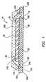
- FIG. 1 iaa side elevational, cross-section view of a preferred embodiment of the semiconductor package of the present invention, wherein depressions are formed on the externally exposed bottom surface of the leads;
- FIG. 2is a bottom plan view of the semiconductor package of FIG. 1;
- FIG. 3is a side elevational, cross section view of the semiconductor package of FIGS. 1 and 2 after the semiconductor package has been connected to a motherboard;
- FIG. 4is a bottom plan view of an alternate embodiment of the semiconductor package of the present invention, wherein depressions are formed on the externally exposed bottom surface of the tie bars;
- FIG. 5is a bottom plan view of an alternate embodiment of the semiconductor package of the present invention, wherein depressions are formed on the externally exposed bottom surface of the chip paddle;
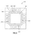
- FIG. 6is a top plan view of a leadframe used to make the semiconductor package of FIG. 1 .
- FIG. 1there is shown a cross sectional view of one embodiment of a semiconductor package constructed in accordance with the principles of the present invention.
- the semiconductor packageincludes a corner 12 and bottom surface 15 .
- the semiconductor packageincludes a semiconductor chip having an upper surface 30 , a circumference 40 and a bottom surface 50 .
- a plurality of input bond pads 60 and output bond pads 70are disposed on the upper surface of the semiconductor chip 20 .
- a chip paddle 80 having a top surface 90 , a side surface 100 and a bottom surface 110is secured to the bottom surface 50 of the semiconductor chip via an adhesive 120 .
- the chip paddle 80has corners 130 , a circumference 140 and may include a half-etched section 150 .
- the half-etched section 150is located at a lower edge 160 of the chip paddle 80 .
- a leadframe 170having a plurality of tie bars 180 , a side surface 190 and a bottom surface 200 .
- the tie bars 180are connected to the corners 130 of the chip paddle 80 and include a bottom section 185 .
- the tie bars 180externally extend from the chip paddle 80 .
- the leadframe 170further has a half-etched section 210 and a plurality of dam bars 220 .
- a plurality of finger-like leads 230are connected to the leadframe 170 and have an upper surface 235 , a side surface 240 and a bottom surface 250 .
- Upper surface 235may, but does not have to be electroplated with gold or silver.
- the leads 230are radially formed at regular intervals along the circumference 140 and spaced apart from the circumference 140 of the chip paddle 80 .
- the leads 230extend towards the chip paddle 80 , such that each of the plurality of leads 230 has a half-etched section 260 facing the chip paddle 80 .
- encapsulation material 280encapsulates the semiconductor chip 20 , conductive wires 270 , chip paddle 80 , and leads 230 .
- Encapsulation material 280may be thermoplastics or thermoset resins, with the thermoset resins including silicones, phenolics, and epoxies.
- the dam bars 220limit the flow of the encapsulation material 280 on the leadframe 170 and provide stability to the leads 230 on the leadframe 170 .
- the chip paddle 80 , leads 230 , and tie bars 180may be externally exposed at the respective side and bottom surfaces.
- the respective half-etched sections 150 , 210 , and 260 of the chip paddle 80 , tie bars, 180 , and leads 240are provided to increase the bonding strength of the encapsulation material 280 in the package 10 . It is contemplated that the respective half-etched sections 150 , 210 , and 260 may be eliminated without departing from the scope and spirit of this invention.
- At least one depression 310is formed on the bottom surface 270 of the leads 250 , which are externally exposed on the bottom surface of the semiconductor package 10 .
- the depressions 310may have various configurations in cross-section, and as such may include but are not limited to rectangular, hemispherical, square, triangular, circular, and omega shapes.
- the depressions 310provide additional area on the bottom surface of the semiconductor package for solder 320 to be applied when the package is secured to a motherboard 330 , best seen in FIG. 3 .
- the variety of cross-sectional configurations of the depression 310support the increased solder joint strength between the motherboard 330 and the package 10 . As shown in FIGS.
- a plurality of depressions 310is preferred to maximize the solder joint strength between the package and the motherboard 330 .
- the solder 320expands into the depression 310 and thereby provides increase interlocking location for the solder 320 to expand when the package is secured to the motherboard 330 .
- the depressions 310may be formed by a chemical etching process, wherein the depressions 310 are contoured when a typical full etching process is conducted to form a general pattern of the leadframe 170 , including the chip paddle 80 , tie bars 180 , leads 230 , and dam bars 220 .
- the depressions 310may be formed after the typical full etching process for the leadframe 170 , wherein the area in which the depressions 310 are to be formed is coated with a photoresist (not shown) while the remaining area of the surface is uncoated. During this alternate process, an enchant (not shown) is sprayed directly over the uncoated area to form the depressions 310 .
- the depressions 310may be formed by mechanical stamping, wherein a punch is applied to the position at which the depressions 310 are to be formed.
- At least one depression 310is formed on the bottom surface 185 of the tie bars 180 .
- at least one depression 310may be formed on the bottom surface 110 of the chip paddle 80 .
- the solder 320 on the bottom surface 110 of the chip paddle 80further increases the heat radiation performance of the semiconductor chip 20 .
- the depressions 310 formed on the tie bars 180 and chip paddle 80may be created by any of the methods described above.
Landscapes
- Physics & Mathematics (AREA)
- Condensed Matter Physics & Semiconductors (AREA)
- General Physics & Mathematics (AREA)
- Engineering & Computer Science (AREA)
- Computer Hardware Design (AREA)
- Microelectronics & Electronic Packaging (AREA)
- Power Engineering (AREA)
- Geometry (AREA)
- Lead Frames For Integrated Circuits (AREA)
Abstract
Description
| First Named | ||
| Attorney Docket No. | Title of Application | Inventor |
| 09/687,487 | Clamp and Heat Block | Young Suk Chung |
| Assembly for Wire | ||
| Bonding a Semiconduc- | ||
| tor Package Assembly | ||
| 09/687,876 | Near Chip Size Semi- | Sean Timothy Crowley |
| conductor Package | ||
| 09/687,495 | Semiconductor Package | Sean Timothy Crowley |
| Improved Locking | ||
| Strength and Its Manu- | ||
| facturing Method | ||
| 09/687,531 | Stackable Semiconductor | Sean Timothy Crowley |
| Package and Method | ||
| for Manufacturing Same | ||
| 09/687,530 | Stackable Semiconductor | Jun Young Yang |
| Package and Method | ||
| for Manufacturing Same | ||
| 09/687,126 | Method of and Apparatus | Hyung Ju Lee |
| for Manufacturing | ||
| Semiconductor Packages | ||
| 09/687,493 | Semiconductor Package | Sung Sik Jang |
| Having Improved Adhe- | ||
| siveness and Ground | ||
| Bonding | ||
| 09/687,541 | Semiconductor Package | Young Suk Chung |
| Leadframe Assembly | ||
| and Method of Manufac- | ||
| ture | ||
Claims (29)
Applications Claiming Priority (2)
| Application Number | Priority Date | Filing Date | Title |
|---|---|---|---|
| KR1019990044659AKR20010037254A (en) | 1999-10-15 | 1999-10-15 | Semiconductor package |
| KR99-44659 | 1999-10-15 |
Publications (1)
| Publication Number | Publication Date |
|---|---|
| US6501161B1true US6501161B1 (en) | 2002-12-31 |
Family
ID=19615442
Family Applications (1)
| Application Number | Title | Priority Date | Filing Date |
|---|---|---|---|
| US09/687,485Expired - LifetimeUS6501161B1 (en) | 1999-10-15 | 2000-10-13 | Semiconductor package having increased solder joint strength |
Country Status (3)
| Country | Link |
|---|---|
| US (1) | US6501161B1 (en) |
| KR (1) | KR20010037254A (en) |
| SG (1) | SG114474A1 (en) |
Cited By (19)
| Publication number | Priority date | Publication date | Assignee | Title |
|---|---|---|---|---|
| US20020140061A1 (en)* | 2001-03-27 | 2002-10-03 | Lee Hyung Ju | Lead frame for semiconductor package |
| US20030173659A1 (en)* | 2002-03-14 | 2003-09-18 | Fairchild Korea Semiconductor Ltd. | Semiconductor package having oxidation-free copper wire |
| US6680524B2 (en)* | 2000-10-26 | 2004-01-20 | Matsushita Electric Industrial Co., Ltd. | Semiconductor device and method for fabricating the same |
| US6686652B1 (en)* | 2000-03-20 | 2004-02-03 | National Semiconductor | Locking lead tips and die attach pad for a leadless package apparatus and method |
| US20060240600A1 (en)* | 2001-12-14 | 2006-10-26 | Fujio Ito | Semiconductor device and method of manufacturing the same |
| US7170149B2 (en)* | 2001-04-13 | 2007-01-30 | Yamaha Corporation | Semiconductor device and package, and method of manufacture therefor |
| US20070063336A1 (en)* | 2005-09-16 | 2007-03-22 | Hase Andreas A | QFN/SON-compatible package |
| US20080067698A1 (en)* | 2006-09-15 | 2008-03-20 | Stats Chippac Ltd. | Integrated circuit package system with encapsulation lock |
| US20080067640A1 (en)* | 2006-09-15 | 2008-03-20 | Stats Chippac Ltd. | Integrated circuit package system with encapsulation lock |
| US20080111219A1 (en)* | 2006-11-14 | 2008-05-15 | Gem Services, Inc. | Package designs for vertical conduction die |
| US20080135991A1 (en)* | 2006-12-12 | 2008-06-12 | Gem Services, Inc. | Semiconductor device package featuring encapsulated leadframe with projecting bumps or balls |
| US20090224387A1 (en)* | 2004-06-30 | 2009-09-10 | Nec Electronics Corporation | Semiconductor chip and method for manufacturing the same and semiconductor device |
| US20090261461A1 (en)* | 2008-04-16 | 2009-10-22 | Steven Sapp | Semiconductor package with lead intrusions |
| US20100117205A1 (en)* | 2006-09-15 | 2010-05-13 | Byung Tai Do | Integrated circuit package system with encapsulation lock and method of manufacture thereof |
| US20100213599A1 (en)* | 2009-02-20 | 2010-08-26 | Kabushiki Kaisha Toshiba | Semiconductor device and manufacturing method thereof |
| US8588017B2 (en) | 2010-10-20 | 2013-11-19 | Samsung Electronics Co., Ltd. | Memory circuits, systems, and modules for performing DRAM refresh operations and methods of operating the same |
| US8809119B1 (en) | 2013-05-17 | 2014-08-19 | Stats Chippac Ltd. | Integrated circuit packaging system with plated leads and method of manufacture thereof |
| US8890301B2 (en) | 2012-08-01 | 2014-11-18 | Analog Devices, Inc. | Packaging and methods for packaging |
| US9048228B2 (en) | 2013-09-26 | 2015-06-02 | Stats Chippac Ltd. | Integrated circuit packaging system with side solderable leads and method of manufacture thereof |
Citations (39)
| Publication number | Priority date | Publication date | Assignee | Title |
|---|---|---|---|---|
| JPS5745959A (en) | 1980-09-02 | 1982-03-16 | Nec Corp | Resin-sealed semiconductor device |
| JPS58101317A (en) | 1981-12-14 | 1983-06-16 | Koike Sanso Kogyo Co Ltd | Rotating positioning device of positioner |
| JPS58160095A (en) | 1982-03-12 | 1983-09-22 | 明産株式会社 | Slitter device automatically positioning slitter knife |
| US4530152A (en) | 1982-04-01 | 1985-07-23 | Compagnie Industrielle Des Telecommunications Cit-Alcatel | Method for encapsulating semiconductor components using temporary substrates |
| JPS6139555A (en) | 1984-07-31 | 1986-02-25 | Toshiba Corp | Resin sealed type semiconductor device with heat sink |
| JPS629639A (en) | 1985-07-05 | 1987-01-17 | Nec Yamagata Ltd | Manufacture of semiconductor device |
| JPS63205935A (en) | 1987-02-23 | 1988-08-25 | Toshiba Corp | Resin-encapsulated semiconductor device with heat sink |
| JPS63233555A (en) | 1987-03-23 | 1988-09-29 | Toshiba Corp | Resin-encapsulated semiconductor device |
| JPS6454749A (en) | 1987-08-26 | 1989-03-02 | Matsushita Electric Industrial Co Ltd | Semiconductor device and manufacture thereof |
| US4987475A (en)* | 1988-02-29 | 1991-01-22 | Digital Equipment Corporation | Alignment of leads for ceramic integrated circuit packages |
| US5041902A (en) | 1989-12-14 | 1991-08-20 | Motorola, Inc. | Molded electronic package with compression structures |
| US5070039A (en)* | 1989-04-13 | 1991-12-03 | Texas Instruments Incorporated | Method of making an integrated circuit using a pre-served dam bar to reduce mold flash and to facilitate flash removal |
| KR920010286A (en) | 1990-11-19 | 1992-06-26 | 존 디. 후써 | A device to shuttle test elements from the discharge path to the cleaning station |
| US5157480A (en) | 1991-02-06 | 1992-10-20 | Motorola, Inc. | Semiconductor device having dual electrical contact sites |
| US5172214A (en) | 1991-02-06 | 1992-12-15 | Motorola, Inc. | Leadless semiconductor device and method for making the same |
| US5172213A (en) | 1991-05-23 | 1992-12-15 | At&T Bell Laboratories | Molded circuit package having heat dissipating post |
| US5250841A (en)* | 1992-04-06 | 1993-10-05 | Motorola, Inc. | Semiconductor device with test-only leads |
| US5278446A (en) | 1992-07-06 | 1994-01-11 | Motorola, Inc. | Reduced stress plastic package |
| US5428248A (en) | 1992-08-21 | 1995-06-27 | Goldstar Electron Co., Ltd. | Resin molded semiconductor package |
| JPH07312405A (en) | 1994-05-17 | 1995-11-28 | Hitachi Ltd | Semiconductor device |
| KR960009774A (en) | 1994-08-06 | 1996-03-22 | 김광호 | Clock fault detection circuit of all electronic switch |
| JPH08125066A (en) | 1994-10-26 | 1996-05-17 | Dainippon Printing Co Ltd | Resin-sealed semiconductor device, lead frame used therefor, and method of manufacturing resin-sealed semiconductor device |
| US5521429A (en) | 1993-11-25 | 1996-05-28 | Sanyo Electric Co., Ltd. | Surface-mount flat package semiconductor device |
| JPH08306853A (en) | 1995-05-09 | 1996-11-22 | Fujitsu Ltd | Semiconductor device, method of manufacturing the same, and method of manufacturing lead frame |
| JPH098206A (en) | 1995-06-19 | 1997-01-10 | Dainippon Printing Co Ltd | Lead frame and bga resin sealed semiconductor device |
| JPH098207A (en) | 1995-06-21 | 1997-01-10 | Dainippon Printing Co Ltd | Resin-sealed semiconductor device |
| JPH098205A (en) | 1995-06-14 | 1997-01-10 | Dainippon Printing Co Ltd | Resin-sealed semiconductor device |
| JPH0992775A (en) | 1995-09-22 | 1997-04-04 | Hitachi Cable Ltd | Semiconductor device |
| US5701034A (en) | 1994-05-03 | 1997-12-23 | Amkor Electronics, Inc. | Packaged semiconductor die including heat sink with locking feature |
| US5783861A (en) | 1994-03-29 | 1998-07-21 | Lg Semicon Co., Ltd. | Semiconductor package and lead frame |
| US5835988A (en) | 1996-03-27 | 1998-11-10 | Mitsubishi Denki Kabushiki Kaisha | Packed semiconductor device with wrap around external leads |
| US5866939A (en) | 1996-01-21 | 1999-02-02 | Anam Semiconductor Inc. | Lead end grid array semiconductor package |
| US5894108A (en) | 1997-02-11 | 1999-04-13 | National Semiconductor Corporation | Plastic package with exposed die |
| US5977613A (en) | 1996-03-07 | 1999-11-02 | Matsushita Electronics Corporation | Electronic component, method for making the same, and lead frame and mold assembly for use therein |
| US5977630A (en) | 1997-08-15 | 1999-11-02 | International Rectifier Corp. | Plural semiconductor die housed in common package with split heat sink |
| US6143981A (en) | 1998-06-24 | 2000-11-07 | Amkor Technology, Inc. | Plastic integrated circuit package and method and leadframe for making the package |
| US6197615B1 (en)* | 1997-04-04 | 2001-03-06 | Samsung Electronics Co., Ltd. | Method of producing lead frame having uneven surfaces |
| US6229200B1 (en)* | 1998-06-10 | 2001-05-08 | Asat Limited | Saw-singulated leadless plastic chip carrier |
| US6294100B1 (en) | 1998-06-10 | 2001-09-25 | Asat Ltd | Exposed die leadless plastic chip carrier |
Family Cites Families (3)
| Publication number | Priority date | Publication date | Assignee | Title |
|---|---|---|---|---|
| JP3012816B2 (en)* | 1996-10-22 | 2000-02-28 | 松下電子工業株式会社 | Resin-sealed semiconductor device and method of manufacturing the same |
| US6281568B1 (en)* | 1998-10-21 | 2001-08-28 | Amkor Technology, Inc. | Plastic integrated circuit device package and leadframe having partially undercut leads and die pad |
| US6208020B1 (en)* | 1999-02-24 | 2001-03-27 | Matsushita Electronics Corporation | Leadframe for use in manufacturing a resin-molded semiconductor device |
- 1999
- 1999-10-15KRKR1019990044659Apatent/KR20010037254A/ennot_activeCeased
- 2000
- 2000-10-13USUS09/687,485patent/US6501161B1/ennot_activeExpired - Lifetime
- 2000-10-16SGSG200005933Apatent/SG114474A1/enunknown
Patent Citations (40)
| Publication number | Priority date | Publication date | Assignee | Title |
|---|---|---|---|---|
| JPS5745959A (en) | 1980-09-02 | 1982-03-16 | Nec Corp | Resin-sealed semiconductor device |
| JPS58101317A (en) | 1981-12-14 | 1983-06-16 | Koike Sanso Kogyo Co Ltd | Rotating positioning device of positioner |
| JPS58160095A (en) | 1982-03-12 | 1983-09-22 | 明産株式会社 | Slitter device automatically positioning slitter knife |
| US4530152A (en) | 1982-04-01 | 1985-07-23 | Compagnie Industrielle Des Telecommunications Cit-Alcatel | Method for encapsulating semiconductor components using temporary substrates |
| JPS6139555A (en) | 1984-07-31 | 1986-02-25 | Toshiba Corp | Resin sealed type semiconductor device with heat sink |
| JPS629639A (en) | 1985-07-05 | 1987-01-17 | Nec Yamagata Ltd | Manufacture of semiconductor device |
| JPS63205935A (en) | 1987-02-23 | 1988-08-25 | Toshiba Corp | Resin-encapsulated semiconductor device with heat sink |
| JPS63233555A (en) | 1987-03-23 | 1988-09-29 | Toshiba Corp | Resin-encapsulated semiconductor device |
| JPS6454749A (en) | 1987-08-26 | 1989-03-02 | Matsushita Electric Industrial Co Ltd | Semiconductor device and manufacture thereof |
| US4987475A (en)* | 1988-02-29 | 1991-01-22 | Digital Equipment Corporation | Alignment of leads for ceramic integrated circuit packages |
| US5070039A (en)* | 1989-04-13 | 1991-12-03 | Texas Instruments Incorporated | Method of making an integrated circuit using a pre-served dam bar to reduce mold flash and to facilitate flash removal |
| US5041902A (en) | 1989-12-14 | 1991-08-20 | Motorola, Inc. | Molded electronic package with compression structures |
| KR920010286A (en) | 1990-11-19 | 1992-06-26 | 존 디. 후써 | A device to shuttle test elements from the discharge path to the cleaning station |
| US5157480A (en) | 1991-02-06 | 1992-10-20 | Motorola, Inc. | Semiconductor device having dual electrical contact sites |
| US5172214A (en) | 1991-02-06 | 1992-12-15 | Motorola, Inc. | Leadless semiconductor device and method for making the same |
| US5172213A (en) | 1991-05-23 | 1992-12-15 | At&T Bell Laboratories | Molded circuit package having heat dissipating post |
| US5250841A (en)* | 1992-04-06 | 1993-10-05 | Motorola, Inc. | Semiconductor device with test-only leads |
| US5278446A (en) | 1992-07-06 | 1994-01-11 | Motorola, Inc. | Reduced stress plastic package |
| US5428248A (en) | 1992-08-21 | 1995-06-27 | Goldstar Electron Co., Ltd. | Resin molded semiconductor package |
| US5521429A (en) | 1993-11-25 | 1996-05-28 | Sanyo Electric Co., Ltd. | Surface-mount flat package semiconductor device |
| US5783861A (en) | 1994-03-29 | 1998-07-21 | Lg Semicon Co., Ltd. | Semiconductor package and lead frame |
| US5701034A (en) | 1994-05-03 | 1997-12-23 | Amkor Electronics, Inc. | Packaged semiconductor die including heat sink with locking feature |
| JPH07312405A (en) | 1994-05-17 | 1995-11-28 | Hitachi Ltd | Semiconductor device |
| KR960009774A (en) | 1994-08-06 | 1996-03-22 | 김광호 | Clock fault detection circuit of all electronic switch |
| JPH08125066A (en) | 1994-10-26 | 1996-05-17 | Dainippon Printing Co Ltd | Resin-sealed semiconductor device, lead frame used therefor, and method of manufacturing resin-sealed semiconductor device |
| JPH08306853A (en) | 1995-05-09 | 1996-11-22 | Fujitsu Ltd | Semiconductor device, method of manufacturing the same, and method of manufacturing lead frame |
| JPH098205A (en) | 1995-06-14 | 1997-01-10 | Dainippon Printing Co Ltd | Resin-sealed semiconductor device |
| JPH098206A (en) | 1995-06-19 | 1997-01-10 | Dainippon Printing Co Ltd | Lead frame and bga resin sealed semiconductor device |
| JPH098207A (en) | 1995-06-21 | 1997-01-10 | Dainippon Printing Co Ltd | Resin-sealed semiconductor device |
| JPH0992775A (en) | 1995-09-22 | 1997-04-04 | Hitachi Cable Ltd | Semiconductor device |
| US5866939A (en) | 1996-01-21 | 1999-02-02 | Anam Semiconductor Inc. | Lead end grid array semiconductor package |
| US5977613A (en) | 1996-03-07 | 1999-11-02 | Matsushita Electronics Corporation | Electronic component, method for making the same, and lead frame and mold assembly for use therein |
| US5835988A (en) | 1996-03-27 | 1998-11-10 | Mitsubishi Denki Kabushiki Kaisha | Packed semiconductor device with wrap around external leads |
| US5894108A (en) | 1997-02-11 | 1999-04-13 | National Semiconductor Corporation | Plastic package with exposed die |
| US6197615B1 (en)* | 1997-04-04 | 2001-03-06 | Samsung Electronics Co., Ltd. | Method of producing lead frame having uneven surfaces |
| US5977630A (en) | 1997-08-15 | 1999-11-02 | International Rectifier Corp. | Plural semiconductor die housed in common package with split heat sink |
| US6229200B1 (en)* | 1998-06-10 | 2001-05-08 | Asat Limited | Saw-singulated leadless plastic chip carrier |
| US6242281B1 (en) | 1998-06-10 | 2001-06-05 | Asat, Limited | Saw-singulated leadless plastic chip carrier |
| US6294100B1 (en) | 1998-06-10 | 2001-09-25 | Asat Ltd | Exposed die leadless plastic chip carrier |
| US6143981A (en) | 1998-06-24 | 2000-11-07 | Amkor Technology, Inc. | Plastic integrated circuit package and method and leadframe for making the package |
Cited By (27)
| Publication number | Priority date | Publication date | Assignee | Title |
|---|---|---|---|---|
| US6686652B1 (en)* | 2000-03-20 | 2004-02-03 | National Semiconductor | Locking lead tips and die attach pad for a leadless package apparatus and method |
| US6680524B2 (en)* | 2000-10-26 | 2004-01-20 | Matsushita Electric Industrial Co., Ltd. | Semiconductor device and method for fabricating the same |
| US6713322B2 (en)* | 2001-03-27 | 2004-03-30 | Amkor Technology, Inc. | Lead frame for semiconductor package |
| US20020140061A1 (en)* | 2001-03-27 | 2002-10-03 | Lee Hyung Ju | Lead frame for semiconductor package |
| US7170149B2 (en)* | 2001-04-13 | 2007-01-30 | Yamaha Corporation | Semiconductor device and package, and method of manufacture therefor |
| US7554182B2 (en)* | 2001-04-13 | 2009-06-30 | Yamaha Corporation | Semiconductor device and package, and method of manufacturer therefor |
| US7507606B2 (en)* | 2001-12-14 | 2009-03-24 | Renesas Technology Corp. | Semiconductor device and method of manufacturing the same |
| US20060240600A1 (en)* | 2001-12-14 | 2006-10-26 | Fujio Ito | Semiconductor device and method of manufacturing the same |
| US20030173659A1 (en)* | 2002-03-14 | 2003-09-18 | Fairchild Korea Semiconductor Ltd. | Semiconductor package having oxidation-free copper wire |
| US20090224387A1 (en)* | 2004-06-30 | 2009-09-10 | Nec Electronics Corporation | Semiconductor chip and method for manufacturing the same and semiconductor device |
| US8786165B2 (en) | 2005-09-16 | 2014-07-22 | Tsmc Solid State Lighting Ltd. | QFN/SON compatible package with SMT land pads |
| US20070063336A1 (en)* | 2005-09-16 | 2007-03-22 | Hase Andreas A | QFN/SON-compatible package |
| US8779568B2 (en) | 2006-09-15 | 2014-07-15 | Stats Chippac Ltd. | Integrated circuit package system with encapsulation lock |
| US8067271B2 (en) | 2006-09-15 | 2011-11-29 | Stats Chippac Ltd. | Integrated circuit package system with encapsulation lock |
| US20080067698A1 (en)* | 2006-09-15 | 2008-03-20 | Stats Chippac Ltd. | Integrated circuit package system with encapsulation lock |
| US20080067640A1 (en)* | 2006-09-15 | 2008-03-20 | Stats Chippac Ltd. | Integrated circuit package system with encapsulation lock |
| US20100117205A1 (en)* | 2006-09-15 | 2010-05-13 | Byung Tai Do | Integrated circuit package system with encapsulation lock and method of manufacture thereof |
| US8093693B2 (en) | 2006-09-15 | 2012-01-10 | Stats Chippac Ltd. | Integrated circuit package system with encapsulation lock |
| US7919838B2 (en)* | 2006-09-15 | 2011-04-05 | Stats Chippac Ltd. | Integrated circuit package system with encapsulation lock and method of manufacture thereof |
| US20080111219A1 (en)* | 2006-11-14 | 2008-05-15 | Gem Services, Inc. | Package designs for vertical conduction die |
| US20080135991A1 (en)* | 2006-12-12 | 2008-06-12 | Gem Services, Inc. | Semiconductor device package featuring encapsulated leadframe with projecting bumps or balls |
| US20090261461A1 (en)* | 2008-04-16 | 2009-10-22 | Steven Sapp | Semiconductor package with lead intrusions |
| US20100213599A1 (en)* | 2009-02-20 | 2010-08-26 | Kabushiki Kaisha Toshiba | Semiconductor device and manufacturing method thereof |
| US8588017B2 (en) | 2010-10-20 | 2013-11-19 | Samsung Electronics Co., Ltd. | Memory circuits, systems, and modules for performing DRAM refresh operations and methods of operating the same |
| US8890301B2 (en) | 2012-08-01 | 2014-11-18 | Analog Devices, Inc. | Packaging and methods for packaging |
| US8809119B1 (en) | 2013-05-17 | 2014-08-19 | Stats Chippac Ltd. | Integrated circuit packaging system with plated leads and method of manufacture thereof |
| US9048228B2 (en) | 2013-09-26 | 2015-06-02 | Stats Chippac Ltd. | Integrated circuit packaging system with side solderable leads and method of manufacture thereof |
Also Published As
| Publication number | Publication date |
|---|---|
| KR20010037254A (en) | 2001-05-07 |
| SG114474A1 (en) | 2005-09-28 |
Similar Documents
| Publication | Publication Date | Title |
|---|---|---|
| US6730544B1 (en) | Stackable semiconductor package and method for manufacturing same | |
| US7045396B2 (en) | Stackable semiconductor package and method for manufacturing same | |
| US7535085B2 (en) | Semiconductor package having improved adhesiveness and ground bonding | |
| US6501161B1 (en) | Semiconductor package having increased solder joint strength | |
| US6696747B1 (en) | Semiconductor package having reduced thickness | |
| US6677663B1 (en) | End grid array semiconductor package | |
| US6646339B1 (en) | Thin and heat radiant semiconductor package and method for manufacturing | |
| US5543657A (en) | Single layer leadframe design with groundplane capability | |
| US7446397B2 (en) | Leadless semiconductor package | |
| TWI453838B (en) | No lead package with heat spreader | |
| US6555899B1 (en) | Semiconductor package leadframe assembly and method of manufacture | |
| US6982485B1 (en) | Stacking structure for semiconductor chips and a semiconductor package using it | |
| US20050205979A1 (en) | Semiconductor package and method for fabricating the same | |
| KR20030018204A (en) | Multi chip package having spacer | |
| US6639308B1 (en) | Near chip size semiconductor package | |
| KR20050109502A (en) | Lead frame with included passive devices | |
| US20070164411A1 (en) | Semiconductor package structure and fabrication method thereof | |
| US6475827B1 (en) | Method for making a semiconductor package having improved defect testing and increased production yield | |
| US6753597B1 (en) | Encapsulated semiconductor package including chip paddle and leads | |
| US6677662B1 (en) | Clamp and heat block assembly for wire bonding a semiconductor package assembly | |
| US7102208B1 (en) | Leadframe and semiconductor package with improved solder joint strength | |
| US6650005B2 (en) | Micro BGA package | |
| KR100250148B1 (en) | VISAI Semiconductor Package | |
| KR200286322Y1 (en) | Semiconductor package | |
| KR20000034120A (en) | LOC type multi-chip package and manufacturing method |
Legal Events
| Date | Code | Title | Description |
|---|---|---|---|
| AS | Assignment | Owner name:AMKOR TECHNOLOGY, INC., ARIZONA Free format text:ASSIGNMENT OF ASSIGNORS INTEREST;ASSIGNOR:LEE, KIL CHIN;REEL/FRAME:011549/0396 Effective date:20010112 | |
| STCF | Information on status: patent grant | Free format text:PATENTED CASE | |
| AS | Assignment | Owner name:CITICORP USA, INC. AS "COLLATERAL AGENT", DELAWARE Free format text:SECURITY INTEREST;ASSIGNORS:AMKOR TECHNOLOGY, INC.;GUARDIAN ASSETS, INC.;REEL/FRAME:013974/0893 Effective date:20030422 | |
| AS | Assignment | Owner name:CITICORP NORTH AMERICA, INC. AS ADMINISTRATIVE AGE Free format text:SECURITY AGREEMENT;ASSIGNORS:AMKOR TECHNOLOGY, INC.;GUARDIAN ASSETS, INC.;REEL/FRAME:014885/0691 Effective date:20040629 | |
| AS | Assignment | Owner name:AMKOR TECHNOLOGY, INC., PENNSYLVANIA Free format text:RELEASE OF LIEN ON PATENTS;ASSIGNOR:CITICORP USA, INC. AS COLLATERAL AGENT;REEL/FRAME:015603/0572 Effective date:20040629 | |
| AS | Assignment | Owner name:CITICORP NORTH AMERICA, INC. AS "AGENT", NEW YORK Free format text:SECURITY AGREEMENT;ASSIGNORS:AMKOR TECHNOLOGY, INC.;GUARDIAN ASSETS, INC.;REEL/FRAME:015942/0521 Effective date:20041027 | |
| AS | Assignment | Owner name:AMKOR TECHNOLOGY, INC., ARIZONA Free format text:TERMINATION & RELEASE OF PATENT SECURITY AGREEMENT;ASSIGNOR:CITICORP NORTH AMERICA, INC.;REEL/FRAME:017388/0868 Effective date:20051128 Owner name:BANK OF AMERICA, N.A., TEXAS Free format text:SECURITY AGREEMENT;ASSIGNOR:AMKOR TECHNOLOGY, INC.;REEL/FRAME:017379/0630 Effective date:20051123 | |
| FPAY | Fee payment | Year of fee payment:4 | |
| FPAY | Fee payment | Year of fee payment:8 | |
| FPAY | Fee payment | Year of fee payment:12 | |
| AS | Assignment | Owner name:BANK OF AMERICA, N.A., AS AGENT, CALIFORNIA Free format text:SECURITY INTEREST;ASSIGNOR:AMKOR TECHNOLOGY, INC.;REEL/FRAME:046683/0139 Effective date:20180713 | |
| AS | Assignment | Owner name:AMKOR TECHNOLOGY SINGAPORE HOLDING PTE.LTD., SINGAPORE Free format text:ASSIGNMENT OF ASSIGNORS INTEREST;ASSIGNOR:AMKOR TECHNOLOGY, INC.;REEL/FRAME:054036/0599 Effective date:20191119 |