US6500351B1 - Process for producing magnetic recording head poles utilizing sputtered materials and a recording head made thereby - Google Patents
Process for producing magnetic recording head poles utilizing sputtered materials and a recording head made therebyDownload PDFInfo
- Publication number
- US6500351B1 US6500351B1US09/317,484US31748499AUS6500351B1US 6500351 B1US6500351 B1US 6500351B1US 31748499 AUS31748499 AUS 31748499AUS 6500351 B1US6500351 B1US 6500351B1
- Authority
- US
- United States
- Prior art keywords
- pole
- iron
- recording head
- magnetic moment
- nitride
- Prior art date
- Legal status (The legal status is an assumption and is not a legal conclusion. Google has not performed a legal analysis and makes no representation as to the accuracy of the status listed.)
- Expired - Fee Related
Links
Images

Classifications
- G—PHYSICS
- G11—INFORMATION STORAGE
- G11B—INFORMATION STORAGE BASED ON RELATIVE MOVEMENT BETWEEN RECORD CARRIER AND TRANSDUCER
- G11B5/00—Recording by magnetisation or demagnetisation of a record carrier; Reproducing by magnetic means; Record carriers therefor
- G11B5/127—Structure or manufacture of heads, e.g. inductive
- G11B5/31—Structure or manufacture of heads, e.g. inductive using thin films
- G11B5/3109—Details
- B—PERFORMING OPERATIONS; TRANSPORTING
- B82—NANOTECHNOLOGY
- B82Y—SPECIFIC USES OR APPLICATIONS OF NANOSTRUCTURES; MEASUREMENT OR ANALYSIS OF NANOSTRUCTURES; MANUFACTURE OR TREATMENT OF NANOSTRUCTURES
- B82Y10/00—Nanotechnology for information processing, storage or transmission, e.g. quantum computing or single electron logic
- B—PERFORMING OPERATIONS; TRANSPORTING
- B82—NANOTECHNOLOGY
- B82Y—SPECIFIC USES OR APPLICATIONS OF NANOSTRUCTURES; MEASUREMENT OR ANALYSIS OF NANOSTRUCTURES; MANUFACTURE OR TREATMENT OF NANOSTRUCTURES
- B82Y25/00—Nanomagnetism, e.g. magnetoimpedance, anisotropic magnetoresistance, giant magnetoresistance or tunneling magnetoresistance
- G—PHYSICS
- G11—INFORMATION STORAGE
- G11B—INFORMATION STORAGE BASED ON RELATIVE MOVEMENT BETWEEN RECORD CARRIER AND TRANSDUCER
- G11B5/00—Recording by magnetisation or demagnetisation of a record carrier; Reproducing by magnetic means; Record carriers therefor
- G11B5/127—Structure or manufacture of heads, e.g. inductive
- G11B5/31—Structure or manufacture of heads, e.g. inductive using thin films
- G11B5/3109—Details
- G11B5/3116—Shaping of layers, poles or gaps for improving the form of the electrical signal transduced, e.g. for shielding, contour effect, equalizing, side flux fringing, cross talk reduction between heads or between heads and information tracks
- G—PHYSICS
- G11—INFORMATION STORAGE
- G11B—INFORMATION STORAGE BASED ON RELATIVE MOVEMENT BETWEEN RECORD CARRIER AND TRANSDUCER
- G11B5/00—Recording by magnetisation or demagnetisation of a record carrier; Reproducing by magnetic means; Record carriers therefor
- G11B5/127—Structure or manufacture of heads, e.g. inductive
- G11B5/31—Structure or manufacture of heads, e.g. inductive using thin films
- G11B5/3163—Fabrication methods or processes specially adapted for a particular head structure, e.g. using base layers for electroplating, using functional layers for masking, using energy or particle beams for shaping the structure or modifying the properties of the basic layers
- G—PHYSICS
- G11—INFORMATION STORAGE
- G11B—INFORMATION STORAGE BASED ON RELATIVE MOVEMENT BETWEEN RECORD CARRIER AND TRANSDUCER
- G11B5/00—Recording by magnetisation or demagnetisation of a record carrier; Reproducing by magnetic means; Record carriers therefor
- G11B5/127—Structure or manufacture of heads, e.g. inductive
- G11B5/33—Structure or manufacture of flux-sensitive heads, i.e. for reproduction only; Combination of such heads with means for recording or erasing only
- G11B5/39—Structure or manufacture of flux-sensitive heads, i.e. for reproduction only; Combination of such heads with means for recording or erasing only using magneto-resistive devices or effects
- G11B5/3903—Structure or manufacture of flux-sensitive heads, i.e. for reproduction only; Combination of such heads with means for recording or erasing only using magneto-resistive devices or effects using magnetic thin film layers or their effects, the films being part of integrated structures
- H—ELECTRICITY
- H01—ELECTRIC ELEMENTS
- H01F—MAGNETS; INDUCTANCES; TRANSFORMERS; SELECTION OF MATERIALS FOR THEIR MAGNETIC PROPERTIES
- H01F41/00—Apparatus or processes specially adapted for manufacturing or assembling magnets, inductances or transformers; Apparatus or processes specially adapted for manufacturing materials characterised by their magnetic properties
- H01F41/14—Apparatus or processes specially adapted for manufacturing or assembling magnets, inductances or transformers; Apparatus or processes specially adapted for manufacturing materials characterised by their magnetic properties for applying magnetic films to substrates
- G—PHYSICS
- G11—INFORMATION STORAGE
- G11B—INFORMATION STORAGE BASED ON RELATIVE MOVEMENT BETWEEN RECORD CARRIER AND TRANSDUCER
- G11B5/00—Recording by magnetisation or demagnetisation of a record carrier; Reproducing by magnetic means; Record carriers therefor
- G11B5/127—Structure or manufacture of heads, e.g. inductive
- G11B5/33—Structure or manufacture of flux-sensitive heads, i.e. for reproduction only; Combination of such heads with means for recording or erasing only
- G11B5/39—Structure or manufacture of flux-sensitive heads, i.e. for reproduction only; Combination of such heads with means for recording or erasing only using magneto-resistive devices or effects
- G11B2005/3996—Structure or manufacture of flux-sensitive heads, i.e. for reproduction only; Combination of such heads with means for recording or erasing only using magneto-resistive devices or effects large or giant magnetoresistive effects [GMR], e.g. as generated in spin-valve [SV] devices
- G—PHYSICS
- G11—INFORMATION STORAGE
- G11B—INFORMATION STORAGE BASED ON RELATIVE MOVEMENT BETWEEN RECORD CARRIER AND TRANSDUCER
- G11B5/00—Recording by magnetisation or demagnetisation of a record carrier; Reproducing by magnetic means; Record carriers therefor
- G11B5/127—Structure or manufacture of heads, e.g. inductive
- G11B5/33—Structure or manufacture of flux-sensitive heads, i.e. for reproduction only; Combination of such heads with means for recording or erasing only
- G11B5/39—Structure or manufacture of flux-sensitive heads, i.e. for reproduction only; Combination of such heads with means for recording or erasing only using magneto-resistive devices or effects
- G11B5/3903—Structure or manufacture of flux-sensitive heads, i.e. for reproduction only; Combination of such heads with means for recording or erasing only using magneto-resistive devices or effects using magnetic thin film layers or their effects, the films being part of integrated structures
- G11B5/3967—Composite structural arrangements of transducers, e.g. inductive write and magnetoresistive read
Definitions
- the present inventionrelates, in general, to the field of magnetoresistive (“MR”) and giant magnetoresistive (“GMR”) recording heads. More particularly, the present invention relates to a process for producing poles in a magnetic recording head utilizing sputtered materials and a magnetic recording head made thereby.
- MRmagnetoresistive
- GMRgiant magnetoresistive
- MR and GMR read headsare known to be useful in reading data from a magnetic surface with a sensitivity exceeding that of inductive or other thin-film heads.
- the sensoris used to detect magnetic field signal changes encoded on a magnetic surface through a change in resistance which is exhibited due to the direction and strength of the associated magnetic flux being sensed.
- the magnetic field signal changes representing the data encoded on the particular storage mediumis “read” by an MR or GMR read head and “written” by a related write, or recording, head.
- the write headmay utilize the “top” shield as a bottom pole thereby providing what is known as a “merged” or “shared” shield pole structure.
- a typical thin film recording headultimately comprises two magnetic poles, a top and bottom pole that surround a coil forming a write gap.
- NiFenickel iron
- permalloynickel iron
- CoZrTacobal-tzirconium-tantalum
- FeAlNiron-aluminum-nitride
- FeTaNiron-tantalum-nitride
- FeNiron nitride
- a magnetic recording head and process for producing the samewherein a relatively high magnetic moment material is sputter deposited or otherwise formed on a substrate.
- a standard photoresist patternis then applied to the high magnetic moment material layer to define the desired pole.
- a first wet chemical etch stepis then utilized to produce a predetermined amount of lateral etch and a predetermined amount of etch depth beneath the photoresist.
- the ratio of the lateral etch to the etch depthis advantageously on the order of 3:1 or greater in order to facilitate the establishment of a substantially discontinuous, or weakly linked, layer of re-deposited material on the sides of the photoresist and high magnetic moment material.
- a subsequent dry etch stepsuch as ion milling, is then used to etch the remaining part of the relatively high magnetic moment material layer using timed etch or end point detection.
- a pre-treatment oxygen plasma step to further reduce the hardened skin of the photoresist prior to a standard photoresist strip stepmay also be used.
- an additional technique in accordance with the disclosure hereinmay be employed wherein a gaseous material, e.g. liquid carbon dioxide (CO 2 ), is employed to further reduce the re-deposited material.
- a gaseous materiale.g. liquid carbon dioxide (CO 2 )
- the liquid carbon dioxidemay be passed through a nozzle through which it is expanded and a substantially steady flow of fast-moving carbon dioxide particles and carbon dioxide gas is formed. By directing this stream at the resultant recording head structure, the particles serve to remove any re-deposited material, which loosened material is then carried away by the carbon dioxide gas.
- a process for producing a magnetic recording head pole and a recording headmade by a process comprising the steps of providing a substrate, forming a layer of relatively high magnetic moment material on a surface of the substrate and patterning a photoresist area on an exposed surface of the formed layer to define the pole. A portion of the exposed surface of the formed layer at least partially underlying the photoresist area is removed to a predetermined lateral width and depth, the formed layer surrounding the photoresist area is further removed to produce the pole, the photoresist area overlying the pole is then stripped away and any re-deposited material remaining on the pole is substantially removed.
- a process for removing re-deposited material in a thin film device structurewhich comprises the steps of providing a source of a gaseous material and directing the gaseous material through a nozzle directed toward the thin film device to produce particles and an associated gas comprising the gaseous material.
- the re-deposited materialis respectively removed and carried away from the device structure by the particles and associated gas.
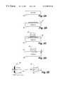
- FIG. 1Aillustrates a conventional process step in the formation of a pole for a magnetic recording head in which the pole is defined by a photoresist area and wherein the structure is then subjected to a dry etching operation, such as ion milling, and which results in the undesired and continuous re-deposition of material on the sides of the pole and the photoresist area;
- a dry etching operationsuch as ion milling
- FIG. 1Billustrates a follow-on operation to the conventional process step shown in FIG. 1A following the stripping of the photoresist area and wherein the re-deposited material adhering to the pole remains as undesired “bunny ears” which promote the formation of voids between them following encapsulation (or overcoat), particularly with the narrow pole widths required for higher areal recording density using relatively high magnetic moment materials;
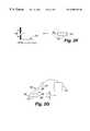
- FIGS. 2A through 2Gillustrate a processing sequence in accordance with an embodiment of the present invention in which a combination of wet and dry etching steps are utilized to first provide an undercut in the relatively high magnetic moment material beneath the photoresist area such that any re-deposition of material on the sides of the pole and photoresist area which occurs during the dry etching step is advantageously rendered substantially discontinuous, or weakly linked, and the re-deposited material remaining on the pole itself following a photoresist strip step can be removed by being subjected to a stream of gaseous particles and carried away by the accompanying gas stream itself.
- FIG. 1Aa conventional process step in the formation of a pole 10 for a magnetic recording head is shown.
- a relatively high magnetic moment material 12has been previously sputtered on a substrate (not shown) and the pole 10 has been defined by an overlying photoresist area.
- the structurehas then been subjected to a dry etching operation, such as ion milling process, and an undesired and continuous re-deposition of the high magnetic moment material 12 comprising re-deposited material 16 can be observed to have occurred on the sides of the pole 10 and the photoresist area 14 .
- a follow-on operation to the conventional process step shown in FIG. 1Ais shown following the stripping of the photoresist area 14 .
- the re-deposited material 16 adhering to the pole 10remains as undesired “bunny ears” 18 which lead to voids in subsequent encapsulation (or overcoat), particularly when used in conjunction with narrow track width heads needed for high density storage devices.
- a substrate 50is provided for subsequent forming of a relatively high magnetic moment material layer 52 as shown in FIG. 2 B.
- the substrate 50may comprise a shared shield with an overlying write gap material on which the MR or GMR writer is formed.
- the relatively high magnetic moment material layer 52may, in a preferred embodiment, be formed in a conventional sputtering operation utilizing cobalt-zirconium-tantalum (CoZrTa), iron-aluminum-nitride (FeAlN), iron-tantalum-nitride (FeTaN), iron-nitride (FeN) or other similar materials.
- CoZrTacobalt-zirconium-tantalum
- FeAlNiron-aluminum-nitride
- FeTaNiron-tantalum-nitride
- FeNiron-nitride
- a wet etching stepis then utilized to remove a portion of the exposed surface of the relatively high magnetic moment material layer 52 surrounding the photoresist area 54 and to provide an under cut in the layer 52 beneath the photoresist area 54 .
- the wet etching operationis advantageously conducted until the undercuts beneath the photoresist area 54 have a lateral width (“X”) which is substantially three times (or greater) than the depth (“Y”) of the material removed from the relatively high magnetic moment material layer 52 .
- X:Ywidth-to-depth ratios
- the ratio X:Ymay be advantageously in the range of substantially 2.2:0.7 microns to 3.2:1.0 microns.
- the structure illustrated in the preceding figureis shown following a dry etching step, such as ion-milling, with the view of the substrate being omitted for purposes of clarity.
- the dry etching stepmay preferably be a timed etch although it is possible that other techniques such as end point detection may be utilized instead.
- the dry etching stepis a relatively long process step which results in the undesired re-deposition of materials, particularly the relatively high magnetic moment material of layer 52 , on the sides of both the relatively high magnetic moment material layer 52 itself as well as on the sides of the photoresist area 54 .
- this layer 56 of re-deposited materialis then rendered as substantially discontinuous or continuous with weak links as shown.
- the re-deposited layer 56is made up of a composite of the relatively high magnetic moment material 52 , photoresist 54 and the substrate 50 . Its thickness is dependent on the amount of material removed by the wet and dry etch steps and the more material that is removed by the wet etch steps results in a thinner re-deposited layer 56 .
- a relatively insignificant amount of the composite material comprising the re-deposited layer 56might be re-deposited on the side of a 4.0 micron thick pole following the 1.0 micron removal of material in a wet etch step.
- the “bunny ear” structures formed utilizing prior art techniquesmight be on the order of 1.0 microns in thickness on a 4.0 micron pole.
- the significant advantage of greatly facilitating the solvent strip of the photoresist area 54is provided as shown in FIG. 2 F. It should be noted that an oxygen plasma process may be carried out to etch away the skin surface of the photoresist area 54 which forms due to the relatively long ion milling operation prior to the photoresist stripping step.
- the re-deposited layer 56still remains on the remaining portion of the relatively high magnetic moment material layer 52 which will ultimately serve as the recording head pole 60 .
- the thickness of the pole 60is generally in the range of 2.0-4.0 ⁇ ).
- the substantially discontinuous portion of the re-deposited material and the weakly linked portion layer 56may then be removed to provide the final pole 60 structure through the provision of a source of gaseous material 62 , for example carbon dioxide (CO 2 ), which is then passed through a nozzle 64 to provide a source of CO 2 particles 66 and an accompanying gas stream 68 and directed at the re-deposited layer 56 as is shown schematically in this figure.
- a source of gaseous material 62for example carbon dioxide (CO 2 )
- CO 2carbon dioxide
- the relatively steady flow of fast moving solid CO 2 particles 66this provides serves to remove the material comprising re-deposited layer 56 from the pole 60 and the material is then swept away from the pole 60 by the accompanying gas stream 68 .
- an ultrasonic de-ionized watermay also be utilized to remove the substantially discontinuous and weakly linked portions of the re-deposited layer 56 .
- a recording head pole production processand a pole made by the process, in which a combination of wet and dry etching steps are utilized to provide an undercut in the relatively high magnetic moment material beneath a photoresist area such that any re-deposited layer of material which occurs on the sides of the pole and photoresist area during the dry etching operation is advantageously rendered substantially discontinuous, or weakly linked, and the re-deposited material remaining on the pole itself following a photoresist strip can then be removed by being subjected to a stream of gaseous particles and ultimately carried away by the accompanying gas stream itself.
Landscapes
- Engineering & Computer Science (AREA)
- Manufacturing & Machinery (AREA)
- Chemical & Material Sciences (AREA)
- Nanotechnology (AREA)
- Crystallography & Structural Chemistry (AREA)
- Power Engineering (AREA)
- Physics & Mathematics (AREA)
- Mathematical Physics (AREA)
- Theoretical Computer Science (AREA)
- Magnetic Heads (AREA)
Abstract
Description
Claims (16)
Priority Applications (2)
| Application Number | Priority Date | Filing Date | Title |
|---|---|---|---|
| US09/317,484US6500351B1 (en) | 1999-05-24 | 1999-05-24 | Process for producing magnetic recording head poles utilizing sputtered materials and a recording head made thereby |
| US10/335,685US6685845B2 (en) | 1999-05-24 | 2002-12-31 | Process for producing magnetic head poles utilizing sputtered materials and a recording head made thereby |
Applications Claiming Priority (1)
| Application Number | Priority Date | Filing Date | Title |
|---|---|---|---|
| US09/317,484US6500351B1 (en) | 1999-05-24 | 1999-05-24 | Process for producing magnetic recording head poles utilizing sputtered materials and a recording head made thereby |
Related Child Applications (1)
| Application Number | Title | Priority Date | Filing Date |
|---|---|---|---|
| US10/335,685DivisionUS6685845B2 (en) | 1999-05-24 | 2002-12-31 | Process for producing magnetic head poles utilizing sputtered materials and a recording head made thereby |
Publications (1)
| Publication Number | Publication Date |
|---|---|
| US6500351B1true US6500351B1 (en) | 2002-12-31 |
Family
ID=23233865
Family Applications (2)
| Application Number | Title | Priority Date | Filing Date |
|---|---|---|---|
| US09/317,484Expired - Fee RelatedUS6500351B1 (en) | 1999-05-24 | 1999-05-24 | Process for producing magnetic recording head poles utilizing sputtered materials and a recording head made thereby |
| US10/335,685Expired - Fee RelatedUS6685845B2 (en) | 1999-05-24 | 2002-12-31 | Process for producing magnetic head poles utilizing sputtered materials and a recording head made thereby |
Family Applications After (1)
| Application Number | Title | Priority Date | Filing Date |
|---|---|---|---|
| US10/335,685Expired - Fee RelatedUS6685845B2 (en) | 1999-05-24 | 2002-12-31 | Process for producing magnetic head poles utilizing sputtered materials and a recording head made thereby |
Country Status (1)
| Country | Link |
|---|---|
| US (2) | US6500351B1 (en) |
Cited By (2)
| Publication number | Priority date | Publication date | Assignee | Title |
|---|---|---|---|---|
| US20050122619A1 (en)* | 2003-12-03 | 2005-06-09 | Seagate Technology Llc | High gradient disc drive writer |
| US8424192B1 (en) | 2005-08-08 | 2013-04-23 | Western Digital (Fremont), Llc | Method for manufacturing a pole for a magnetic recording head |
Families Citing this family (2)
| Publication number | Priority date | Publication date | Assignee | Title |
|---|---|---|---|---|
| US7396769B2 (en)* | 2004-08-02 | 2008-07-08 | Lam Research Corporation | Method for stripping photoresist from etched wafer |
| US7623325B2 (en)* | 2005-09-29 | 2009-11-24 | Hitachi Global Storage Technologies Netherlands B.V. | Method for providing an endpoint layer for ion milling of top of read sensor having top lead connection and sensor formed thereby |
Citations (20)
| Publication number | Priority date | Publication date | Assignee | Title |
|---|---|---|---|---|
| US4443294A (en)* | 1981-06-10 | 1984-04-17 | Hitachi, Ltd. | Process for forming magnetic film pattern |
| US4529860A (en)* | 1982-08-02 | 1985-07-16 | Motorola, Inc. | Plasma etching of organic materials |
| US4970616A (en) | 1988-08-17 | 1990-11-13 | Digital Equipment Corporation | Recording head to minimize undershoots in readback pulses |
| US5315793A (en) | 1991-10-01 | 1994-05-31 | Hughes Aircraft Company | System for precision cleaning by jet spray |
| JPH0721533A (en)* | 1993-07-05 | 1995-01-24 | Sumitomo Metal Ind Ltd | Method of manufacturing thin film magnetic head |
| JPH08180330A (en)* | 1994-12-27 | 1996-07-12 | Nec Corp | Production of magnetoresistive effect type reading converter |
| US5639509A (en) | 1995-06-05 | 1997-06-17 | Quantum Peripherals Colorado, Inc. | Process for forming a flux enhanced magnetic data transducer |
| US5705443A (en)* | 1995-05-30 | 1998-01-06 | Advanced Technology Materials, Inc. | Etching method for refractory materials |
| US5733820A (en)* | 1995-04-27 | 1998-03-31 | Sharp Kabushiki Kaisha | Dry etching method |
| US5753131A (en)* | 1995-06-30 | 1998-05-19 | Samsung Electronics Co., Ltd. | Magnetoresistive device and manufacturing method thereof |
| US5793579A (en)* | 1995-11-30 | 1998-08-11 | Sanyo Electric Co., Ltd. | Thin film magnetic head and process for producing same |
| US5804085A (en)* | 1997-01-30 | 1998-09-08 | Quantum Corporation | Process for producing a pole-trimmed writer in a magnetoresistive read/write head and a data transducer made thereby |
| US5867890A (en)* | 1997-12-17 | 1999-02-09 | International Business Machines Corporation | Method for making a thin film merged magnetoresistive read/inductive write head having a pedestal pole tip |
| US5874010A (en)* | 1996-07-17 | 1999-02-23 | Headway Technologies, Inc. | Pole trimming technique for high data rate thin film heads |
| US5893981A (en)* | 1996-06-17 | 1999-04-13 | International Business Machines Corporation | Method of making stabilized MR sensor and flux guide joined by contiguous junction |
| US5916423A (en)* | 1997-05-06 | 1999-06-29 | International Business Machines Corporation | P1 notched write head with minimum overmilled p1 and p2 |
| US5935453A (en)* | 1995-11-16 | 1999-08-10 | International Business Machines Corporation | MR sensor having end regions with planar sides |
| US5938941A (en)* | 1996-10-04 | 1999-08-17 | Nec Corporation | Magnetoresistance effect composite head and method of forming the same |
| US6007731A (en)* | 1998-03-23 | 1999-12-28 | Headway Technologies, Inc. | Soft adjacent layer (SAL) magnetoresistive (MR) sensor element with electrically insulated soft adjacent layer (SAL) |
| US6069775A (en)* | 1997-12-22 | 2000-05-30 | International Business Machines Corporation | Inverted merged MR head with precise track width |
- 1999
- 1999-05-24USUS09/317,484patent/US6500351B1/ennot_activeExpired - Fee Related
- 2002
- 2002-12-31USUS10/335,685patent/US6685845B2/ennot_activeExpired - Fee Related
Patent Citations (22)
| Publication number | Priority date | Publication date | Assignee | Title |
|---|---|---|---|---|
| US4443294A (en)* | 1981-06-10 | 1984-04-17 | Hitachi, Ltd. | Process for forming magnetic film pattern |
| US4529860A (en)* | 1982-08-02 | 1985-07-16 | Motorola, Inc. | Plasma etching of organic materials |
| US4970616A (en) | 1988-08-17 | 1990-11-13 | Digital Equipment Corporation | Recording head to minimize undershoots in readback pulses |
| US5315793A (en) | 1991-10-01 | 1994-05-31 | Hughes Aircraft Company | System for precision cleaning by jet spray |
| JPH0721533A (en)* | 1993-07-05 | 1995-01-24 | Sumitomo Metal Ind Ltd | Method of manufacturing thin film magnetic head |
| JPH08180330A (en)* | 1994-12-27 | 1996-07-12 | Nec Corp | Production of magnetoresistive effect type reading converter |
| US5733820A (en)* | 1995-04-27 | 1998-03-31 | Sharp Kabushiki Kaisha | Dry etching method |
| US5705443A (en)* | 1995-05-30 | 1998-01-06 | Advanced Technology Materials, Inc. | Etching method for refractory materials |
| US5639509A (en) | 1995-06-05 | 1997-06-17 | Quantum Peripherals Colorado, Inc. | Process for forming a flux enhanced magnetic data transducer |
| US5751526A (en) | 1995-06-05 | 1998-05-12 | Mke-Quantum Components Colorado Llc | Flux enhanced write transducer and process for producing the same in conjunction with shared shields on magnetoresistive read heads |
| US5753131A (en)* | 1995-06-30 | 1998-05-19 | Samsung Electronics Co., Ltd. | Magnetoresistive device and manufacturing method thereof |
| US5935453A (en)* | 1995-11-16 | 1999-08-10 | International Business Machines Corporation | MR sensor having end regions with planar sides |
| US5793579A (en)* | 1995-11-30 | 1998-08-11 | Sanyo Electric Co., Ltd. | Thin film magnetic head and process for producing same |
| US5893981A (en)* | 1996-06-17 | 1999-04-13 | International Business Machines Corporation | Method of making stabilized MR sensor and flux guide joined by contiguous junction |
| US5874010A (en)* | 1996-07-17 | 1999-02-23 | Headway Technologies, Inc. | Pole trimming technique for high data rate thin film heads |
| US5938941A (en)* | 1996-10-04 | 1999-08-17 | Nec Corporation | Magnetoresistance effect composite head and method of forming the same |
| US5804085A (en)* | 1997-01-30 | 1998-09-08 | Quantum Corporation | Process for producing a pole-trimmed writer in a magnetoresistive read/write head and a data transducer made thereby |
| US5916423A (en)* | 1997-05-06 | 1999-06-29 | International Business Machines Corporation | P1 notched write head with minimum overmilled p1 and p2 |
| US6106679A (en)* | 1997-05-06 | 2000-08-22 | International Business Machines Corporation | Method of making P1 notched write head with minimum overmilled P1 and P2 |
| US5867890A (en)* | 1997-12-17 | 1999-02-09 | International Business Machines Corporation | Method for making a thin film merged magnetoresistive read/inductive write head having a pedestal pole tip |
| US6069775A (en)* | 1997-12-22 | 2000-05-30 | International Business Machines Corporation | Inverted merged MR head with precise track width |
| US6007731A (en)* | 1998-03-23 | 1999-12-28 | Headway Technologies, Inc. | Soft adjacent layer (SAL) magnetoresistive (MR) sensor element with electrically insulated soft adjacent layer (SAL) |
Cited By (3)
| Publication number | Priority date | Publication date | Assignee | Title |
|---|---|---|---|---|
| US20050122619A1 (en)* | 2003-12-03 | 2005-06-09 | Seagate Technology Llc | High gradient disc drive writer |
| US7187519B2 (en) | 2003-12-03 | 2007-03-06 | Seagate Technology Llc | High gradient disc drive writer |
| US8424192B1 (en) | 2005-08-08 | 2013-04-23 | Western Digital (Fremont), Llc | Method for manufacturing a pole for a magnetic recording head |
Also Published As
| Publication number | Publication date |
|---|---|
| US6685845B2 (en) | 2004-02-03 |
| US20030094432A1 (en) | 2003-05-22 |
Similar Documents
| Publication | Publication Date | Title |
|---|---|---|
| US6141183A (en) | Process for producing a pole-trimmed writer in a magnetoresistive read/write head and a data transducer made thereby | |
| US5404635A (en) | Method of making a narrow track thin film head | |
| US5639509A (en) | Process for forming a flux enhanced magnetic data transducer | |
| US7995307B2 (en) | Perpendicular magnetic recording write head with trailing shield having throat height defined by electroplated nonmagnetic pad layer and method for making the head | |
| US5363265A (en) | Planarized magnetoresistive sensor | |
| KR100243822B1 (en) | Magnetoresistive sensor and the method of preparing a magnetoresistive sensor | |
| US7352539B2 (en) | Thin-film magnetic head having a covered insulating layer | |
| EP0383739B1 (en) | Method for making thin film magnetic head | |
| JPH11273027A (en) | Manufacturing method of composite type thin film magnetic head and magneto-resistance head structure and composite type thin film magnetic head | |
| JPH0150007B2 (en) | ||
| US7050273B2 (en) | Bottom spin valve sensor having a lead overlay (LOL) structure fabricated thereon | |
| US5774308A (en) | Thin film inductive head and magnetic writing/reading drive including the same | |
| US6678940B2 (en) | Method of making a thin-film magnetic head | |
| US7377024B2 (en) | Method of making a magnetic write head with trailing shield throat pad | |
| US6673633B2 (en) | Method of forming patterned thin film and method of manufacturing thin-film magnetic head | |
| US6500351B1 (en) | Process for producing magnetic recording head poles utilizing sputtered materials and a recording head made thereby | |
| US7005242B2 (en) | Magnetic head and method of making the same using an etch-stop layer for removing portions of the capping layer | |
| US20030199233A1 (en) | Thin-film magnetic head and method of forming the same | |
| JPH10247305A (en) | Production of composite type thin-film magnetic head | |
| US7141508B2 (en) | Magnetoresistive effect thin-film magnetic head and manufacturing method of magnetoresistive effect thin-film magnetic head | |
| US7207098B2 (en) | Hard mask method of forming a reader of a magnetic head | |
| US20030219980A1 (en) | Pattern forming method, method of making microdevice, method of making thin-film magnetic head, method of making magnetic head slider, method of making magnetic head apparatus, and method of making magnetic recording and reproducing apparatus | |
| JP2861080B2 (en) | Method for forming pattern of amorphous alloy magnetic film | |
| JP2000339624A (en) | Production of thin film magnetic head | |
| JPH06267031A (en) | Magnetoresistive head and manufacturing method thereof |
Legal Events
| Date | Code | Title | Description |
|---|---|---|---|
| AS | Assignment | Owner name:QUANTUM CORPORATION, CALIFORNIA Free format text:ASSIGNMENT OF ASSIGNORS INTEREST;ASSIGNORS:WU, ANDREW L.;GREIMAN, JEFFREY G.;NEUMANN, LAWRENCE G.;AND OTHERS;REEL/FRAME:009989/0686 Effective date:19990514 | |
| AS | Assignment | Owner name:MAXTOR CORPORATION, CALIFORNIA Free format text:ASSIGNMENT OF ASSIGNORS INTEREST;ASSIGNOR:QUANTUM CORPORATION;REEL/FRAME:012653/0726 Effective date:20010724 | |
| FPAY | Fee payment | Year of fee payment:4 | |
| AS | Assignment | Owner name:WELLS FARGO BANK, NATIONAL ASSOCIATION, AS COLLATERAL AGENT AND SECOND PRIORITY REPRESENTATIVE, CALIFORNIA Free format text:SECURITY AGREEMENT;ASSIGNORS:MAXTOR CORPORATION;SEAGATE TECHNOLOGY LLC;SEAGATE TECHNOLOGY INTERNATIONAL;REEL/FRAME:022757/0017 Effective date:20090507 Owner name:JPMORGAN CHASE BANK, N.A., AS ADMINISTRATIVE AGENT AND FIRST PRIORITY REPRESENTATIVE, NEW YORK Free format text:SECURITY AGREEMENT;ASSIGNORS:MAXTOR CORPORATION;SEAGATE TECHNOLOGY LLC;SEAGATE TECHNOLOGY INTERNATIONAL;REEL/FRAME:022757/0017 Effective date:20090507 Owner name:JPMORGAN CHASE BANK, N.A., AS ADMINISTRATIVE AGENT Free format text:SECURITY AGREEMENT;ASSIGNORS:MAXTOR CORPORATION;SEAGATE TECHNOLOGY LLC;SEAGATE TECHNOLOGY INTERNATIONAL;REEL/FRAME:022757/0017 Effective date:20090507 Owner name:WELLS FARGO BANK, NATIONAL ASSOCIATION, AS COLLATE Free format text:SECURITY AGREEMENT;ASSIGNORS:MAXTOR CORPORATION;SEAGATE TECHNOLOGY LLC;SEAGATE TECHNOLOGY INTERNATIONAL;REEL/FRAME:022757/0017 Effective date:20090507 | |
| FPAY | Fee payment | Year of fee payment:8 | |
| AS | Assignment | Owner name:MAXTOR CORPORATION, CALIFORNIA Free format text:RELEASE;ASSIGNOR:JPMORGAN CHASE BANK, N.A., AS ADMINISTRATIVE AGENT;REEL/FRAME:025662/0001 Effective date:20110114 Owner name:SEAGATE TECHNOLOGY LLC, CALIFORNIA Free format text:RELEASE;ASSIGNOR:JPMORGAN CHASE BANK, N.A., AS ADMINISTRATIVE AGENT;REEL/FRAME:025662/0001 Effective date:20110114 Owner name:SEAGATE TECHNOLOGY HDD HOLDINGS, CALIFORNIA Free format text:RELEASE;ASSIGNOR:JPMORGAN CHASE BANK, N.A., AS ADMINISTRATIVE AGENT;REEL/FRAME:025662/0001 Effective date:20110114 Owner name:SEAGATE TECHNOLOGY INTERNATIONAL, CALIFORNIA Free format text:RELEASE;ASSIGNOR:JPMORGAN CHASE BANK, N.A., AS ADMINISTRATIVE AGENT;REEL/FRAME:025662/0001 Effective date:20110114 | |
| AS | Assignment | Owner name:THE BANK OF NOVA SCOTIA, AS ADMINISTRATIVE AGENT, CANADA Free format text:SECURITY AGREEMENT;ASSIGNOR:SEAGATE TECHNOLOGY LLC;REEL/FRAME:026010/0350 Effective date:20110118 Owner name:THE BANK OF NOVA SCOTIA, AS ADMINISTRATIVE AGENT, Free format text:SECURITY AGREEMENT;ASSIGNOR:SEAGATE TECHNOLOGY LLC;REEL/FRAME:026010/0350 Effective date:20110118 | |
| AS | Assignment | Owner name:SEAGATE TECHNOLOGY INTERNATIONAL, CAYMAN ISLANDS Free format text:TERMINATION AND RELEASE OF SECURITY INTEREST IN PATENT RIGHTS;ASSIGNOR:WELLS FARGO BANK, NATIONAL ASSOCIATION, AS COLLATERAL AGENT AND SECOND PRIORITY REPRESENTATIVE;REEL/FRAME:030833/0001 Effective date:20130312 Owner name:EVAULT INC. (F/K/A I365 INC.), CALIFORNIA Free format text:TERMINATION AND RELEASE OF SECURITY INTEREST IN PATENT RIGHTS;ASSIGNOR:WELLS FARGO BANK, NATIONAL ASSOCIATION, AS COLLATERAL AGENT AND SECOND PRIORITY REPRESENTATIVE;REEL/FRAME:030833/0001 Effective date:20130312 Owner name:SEAGATE TECHNOLOGY LLC, CALIFORNIA Free format text:TERMINATION AND RELEASE OF SECURITY INTEREST IN PATENT RIGHTS;ASSIGNOR:WELLS FARGO BANK, NATIONAL ASSOCIATION, AS COLLATERAL AGENT AND SECOND PRIORITY REPRESENTATIVE;REEL/FRAME:030833/0001 Effective date:20130312 Owner name:SEAGATE TECHNOLOGY US HOLDINGS, INC., CALIFORNIA Free format text:TERMINATION AND RELEASE OF SECURITY INTEREST IN PATENT RIGHTS;ASSIGNOR:WELLS FARGO BANK, NATIONAL ASSOCIATION, AS COLLATERAL AGENT AND SECOND PRIORITY REPRESENTATIVE;REEL/FRAME:030833/0001 Effective date:20130312 | |
| REMI | Maintenance fee reminder mailed | ||
| LAPS | Lapse for failure to pay maintenance fees | ||
| STCH | Information on status: patent discontinuation | Free format text:PATENT EXPIRED DUE TO NONPAYMENT OF MAINTENANCE FEES UNDER 37 CFR 1.362 | |
| FP | Lapsed due to failure to pay maintenance fee | Effective date:20141231 | |
| AS | Assignment | Owner name:SEAGATE TECHNOLOGY PUBLIC LIMITED COMPANY, CALIFORNIA Free format text:RELEASE BY SECURED PARTY;ASSIGNOR:THE BANK OF NOVA SCOTIA;REEL/FRAME:072193/0001 Effective date:20250303 Owner name:SEAGATE TECHNOLOGY, CALIFORNIA Free format text:RELEASE BY SECURED PARTY;ASSIGNOR:THE BANK OF NOVA SCOTIA;REEL/FRAME:072193/0001 Effective date:20250303 Owner name:SEAGATE TECHNOLOGY HDD HOLDINGS, CALIFORNIA Free format text:RELEASE BY SECURED PARTY;ASSIGNOR:THE BANK OF NOVA SCOTIA;REEL/FRAME:072193/0001 Effective date:20250303 Owner name:I365 INC., CALIFORNIA Free format text:RELEASE BY SECURED PARTY;ASSIGNOR:THE BANK OF NOVA SCOTIA;REEL/FRAME:072193/0001 Effective date:20250303 Owner name:SEAGATE TECHNOLOGY LLC, CALIFORNIA Free format text:RELEASE BY SECURED PARTY;ASSIGNOR:THE BANK OF NOVA SCOTIA;REEL/FRAME:072193/0001 Effective date:20250303 Owner name:SEAGATE TECHNOLOGY INTERNATIONAL, CAYMAN ISLANDS Free format text:RELEASE BY SECURED PARTY;ASSIGNOR:THE BANK OF NOVA SCOTIA;REEL/FRAME:072193/0001 Effective date:20250303 Owner name:SEAGATE HDD CAYMAN, CAYMAN ISLANDS Free format text:RELEASE BY SECURED PARTY;ASSIGNOR:THE BANK OF NOVA SCOTIA;REEL/FRAME:072193/0001 Effective date:20250303 Owner name:SEAGATE TECHNOLOGY (US) HOLDINGS, INC., CALIFORNIA Free format text:RELEASE BY SECURED PARTY;ASSIGNOR:THE BANK OF NOVA SCOTIA;REEL/FRAME:072193/0001 Effective date:20250303 |