US6498381B2 - Semiconductor structures having multiple conductive layers in an opening, and methods for fabricating same - Google Patents
Semiconductor structures having multiple conductive layers in an opening, and methods for fabricating sameDownload PDFInfo
- Publication number
- US6498381B2 US6498381B2US09/792,311US79231101AUS6498381B2US 6498381 B2US6498381 B2US 6498381B2US 79231101 AUS79231101 AUS 79231101AUS 6498381 B2US6498381 B2US 6498381B2
- Authority
- US
- United States
- Prior art keywords
- opening
- substrate
- conductive layer
- conductive
- circuit structure
- Prior art date
- Legal status (The legal status is an assumption and is not a legal conclusion. Google has not performed a legal analysis and makes no representation as to the accuracy of the status listed.)
- Expired - Lifetime
Links
Images


Classifications
- H—ELECTRICITY
- H01—ELECTRIC ELEMENTS
- H01L—SEMICONDUCTOR DEVICES NOT COVERED BY CLASS H10
- H01L21/00—Processes or apparatus adapted for the manufacture or treatment of semiconductor or solid state devices or of parts thereof
- H01L21/70—Manufacture or treatment of devices consisting of a plurality of solid state components formed in or on a common substrate or of parts thereof; Manufacture of integrated circuit devices or of parts thereof
- H01L21/71—Manufacture of specific parts of devices defined in group H01L21/70
- H01L21/768—Applying interconnections to be used for carrying current between separate components within a device comprising conductors and dielectrics
- H—ELECTRICITY
- H01—ELECTRIC ELEMENTS
- H01L—SEMICONDUCTOR DEVICES NOT COVERED BY CLASS H10
- H01L23/00—Details of semiconductor or other solid state devices
- H01L23/552—Protection against radiation, e.g. light or electromagnetic waves
- H—ELECTRICITY
- H01—ELECTRIC ELEMENTS
- H01L—SEMICONDUCTOR DEVICES NOT COVERED BY CLASS H10
- H01L21/00—Processes or apparatus adapted for the manufacture or treatment of semiconductor or solid state devices or of parts thereof
- H01L21/70—Manufacture or treatment of devices consisting of a plurality of solid state components formed in or on a common substrate or of parts thereof; Manufacture of integrated circuit devices or of parts thereof
- H01L21/71—Manufacture of specific parts of devices defined in group H01L21/70
- H01L21/768—Applying interconnections to be used for carrying current between separate components within a device comprising conductors and dielectrics
- H01L21/76898—Applying interconnections to be used for carrying current between separate components within a device comprising conductors and dielectrics formed through a semiconductor substrate
- H—ELECTRICITY
- H01—ELECTRIC ELEMENTS
- H01L—SEMICONDUCTOR DEVICES NOT COVERED BY CLASS H10
- H01L23/00—Details of semiconductor or other solid state devices
- H01L23/48—Arrangements for conducting electric current to or from the solid state body in operation, e.g. leads, terminal arrangements ; Selection of materials therefor
- H01L23/481—Internal lead connections, e.g. via connections, feedthrough structures
- H—ELECTRICITY
- H01—ELECTRIC ELEMENTS
- H01L—SEMICONDUCTOR DEVICES NOT COVERED BY CLASS H10
- H01L2223/00—Details relating to semiconductor or other solid state devices covered by the group H01L23/00
- H01L2223/58—Structural electrical arrangements for semiconductor devices not otherwise provided for
- H01L2223/64—Impedance arrangements
- H01L2223/66—High-frequency adaptations
- H01L2223/6605—High-frequency electrical connections
- H01L2223/6616—Vertical connections, e.g. vias
- H01L2223/6622—Coaxial feed-throughs in active or passive substrates
- H—ELECTRICITY
- H01—ELECTRIC ELEMENTS
- H01L—SEMICONDUCTOR DEVICES NOT COVERED BY CLASS H10
- H01L2224/00—Indexing scheme for arrangements for connecting or disconnecting semiconductor or solid-state bodies and methods related thereto as covered by H01L24/00
- H01L2224/01—Means for bonding being attached to, or being formed on, the surface to be connected, e.g. chip-to-package, die-attach, "first-level" interconnects; Manufacturing methods related thereto
- H01L2224/10—Bump connectors; Manufacturing methods related thereto
- H01L2224/15—Structure, shape, material or disposition of the bump connectors after the connecting process
- H01L2224/16—Structure, shape, material or disposition of the bump connectors after the connecting process of an individual bump connector
- H—ELECTRICITY
- H01—ELECTRIC ELEMENTS
- H01L—SEMICONDUCTOR DEVICES NOT COVERED BY CLASS H10
- H01L2924/00—Indexing scheme for arrangements or methods for connecting or disconnecting semiconductor or solid-state bodies as covered by H01L24/00
- H01L2924/049—Nitrides composed of metals from groups of the periodic table
- H01L2924/0494—4th Group
- H01L2924/04941—TiN
- H—ELECTRICITY
- H01—ELECTRIC ELEMENTS
- H01L—SEMICONDUCTOR DEVICES NOT COVERED BY CLASS H10
- H01L2924/00—Indexing scheme for arrangements or methods for connecting or disconnecting semiconductor or solid-state bodies as covered by H01L24/00
- H01L2924/10—Details of semiconductor or other solid state devices to be connected
- H01L2924/11—Device type
- H01L2924/12—Passive devices, e.g. 2 terminal devices
- H01L2924/1203—Rectifying Diode
- H01L2924/12032—Schottky diode
- H—ELECTRICITY
- H01—ELECTRIC ELEMENTS
- H01L—SEMICONDUCTOR DEVICES NOT COVERED BY CLASS H10
- H01L2924/00—Indexing scheme for arrangements or methods for connecting or disconnecting semiconductor or solid-state bodies as covered by H01L24/00
- H01L2924/30—Technical effects
- H01L2924/301—Electrical effects
- H01L2924/3025—Electromagnetic shielding
- Y—GENERAL TAGGING OF NEW TECHNOLOGICAL DEVELOPMENTS; GENERAL TAGGING OF CROSS-SECTIONAL TECHNOLOGIES SPANNING OVER SEVERAL SECTIONS OF THE IPC; TECHNICAL SUBJECTS COVERED BY FORMER USPC CROSS-REFERENCE ART COLLECTIONS [XRACs] AND DIGESTS
- Y10—TECHNICAL SUBJECTS COVERED BY FORMER USPC
- Y10S—TECHNICAL SUBJECTS COVERED BY FORMER USPC CROSS-REFERENCE ART COLLECTIONS [XRACs] AND DIGESTS
- Y10S438/00—Semiconductor device manufacturing: process
- Y10S438/977—Thinning or removal of substrate
Definitions
- the present inventionrelates to semiconductor technology.
- Some embodiments of the inventionfacilitate creation of electromagnetic shielding for circuit nodes that carry AC (alternating current) signals. Such shielding advantageously reduces energy losses for the AC signals. The shielding also reduces noise in shielded regions.
- Some embodimentsallow fabrication of capacitors and capacitor networks in a small area.
- a circuit manufacturing methodcomprises:
- the conductive layersincluding a first conductive layer and a second conductive layer overlaying the first conductive layer such that the first and second conductive layers either (i) are separated by an insulating layer in the opening, or (ii) form a P-N junction in the opening, or (iii) form a Schottky junction in the opening;
- the first and second conductive layersare separated by an insulating layer in the opening.
- the first conductive layershields the substrate from AC signals carried by a contact pad made from the second conductive layer on a wafer backside.
- Contact pads on the wafer backsidecan facilitate vertical integration and small scale packaging.
- the first and second conductive layersprovide conductive plates of a capacitor.
- the inventionprovides a circuit structure comprising a semiconductor substrate, an opening passing through the substrate between a first side of the substrate and a second side of the substrate, and a plurality of conductive layers which overlay sidewalls of the opening, wherein the conductive layers include a first conductive layer and a second conductive layer such that the first and second conductive layers either (i) are separated by an insulating layer in the opening, or (ii) form a P-N junction in the opening, or (iii) form a Schottky junction in the opening; wherein the second conductive layer is exposed on the second side of the opening, and the first conductive layer surrounds the second conductive layer in the opening.
- a circuit manufacturing methodcomprises:
- each two consecutive conductive layerseither (i) are separated by an insulating layer in the opening, or (ii) form a P-N junction in the opening, or (iii) form a Schottky junction in the opening;
- a circuit structurecomprises:
- each two adjacent conductive layerseither (i) form a P-N junction in the opening, or (ii) form a Schottky junction in the opening, or (iii) are separated by an insulating layer in the opening;
- a circuit manufacturing methodcomprises:
- the conductive layersincluding a first conductive layer and a second conductive layer overlaying the first conductive layer such that the first and second conductive layers either (i) form a P-N junction, or (ii) form a Schottky diode junction;
- a circuit structurecomprises:
- the conductive layersincluding first and second conductive layers which either (i) form a P-N junction in the opening, or (ii) form a Schottky junction in the opening;
- FIGS. 1-4Aare vertical cross-sectional views of structures according to the present invention.
- FIG. 4Bis a horizontal cross-sectional view of the structure of FIG. 4 A.
- FIGS. 5-17are vertical cross-sectional views of structures according to the present invention.
- FIGS. 18-22are circuit diagrams corresponding to structures according to the present invention.
- FIG. 23Ais a vertical cross-sectional view of a structure according to the present invention.
- FIGS. 23B, 23 C, 24are circuit diagrams corresponding to structures according to the present invention.
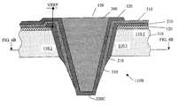
- FIG. 1illustrates a semiconductor wafer 110 which will include one or more backside contact pads.
- the waferhas been processed to form transistors, capacitors, resistors, conductive lines, and/or other circuit elements, or portions of circuit elements (not shown). Circuit elements fabricated in, above, or below the substrate 110 can be present.
- An insulating layer 120has been formed on the wafer. In some embodiments, insulator 120 is used in other portions of the wafer to form the circuit elements mentioned above. In some embodiments, insulator 120 is omitted.
- each opening 130is etched in the wafer through the insulator 120 .
- the depth of each opening 130exceeds the final thickness of the wafer at the location of the opening (the wafer will be thinned as described below).
- the lateral shape and dimensions of each opening 130correspond to the desired shape and dimensions of a backside contact pad to be formed in the opening. In some embodiments, the depth D 1 of each opening 130 is about 100 ⁇ m.
- At least some of the openings 130are shaped as an inverted truncated cone having a top diameter D 2 of 30-50 ⁇ m, or an inverted truncated pyramid whose top surface is a square of a side of 30-50 ⁇ m.
- An openingmay also be shaped as a non-inverted truncated cone or pyramid or as a cylinder.
- An openingmay have a rounded bottom. For example, hemispherical openings are used in some embodiments.
- An openingmay be elongated (as a groove). Other shapes and dimensions are possible. Different openings 130 may have different shapes and dimensions in the same wafer.
- Suitable processes for forming the openings 130are described in the aforementioned PCT publication WO 98/19337.
- the mask (not shown) for etching the openingscan be made of photolithographically patterned aluminum. The invention is not limited to any particular process.
- a conductive layer 210(FIG. 2) is formed over the wafer.
- Layer 210will provide electromagnetic shielding in openings 130 .
- Layer 210overlays the sidewalls of openings 130 .
- Layer 210can be photolithographically patterned if desired.
- an insulating layer 310(FIG. 3) and a conductive layer 320 are formed over the wafer. These layers can be patterned as desired. in some embodiments, the layers 210 , 310 , 320 completely cover the inner surface (sidewalls and bottom) of each opening 130 .
- the openings 130can be completely or partially filled by some material 340 for increased mechanical strength and, possibly, increased electrical and thermal conductivity. Both conductive and insulating materials can be used. See the aforementioned PCT publication WO 98/19337. In other embodiments, the openings are filled with a plug made from layer 320 . In other embodiments, the openings are not filled.
- FIGS. 1-3formation of openings 130 and layers 120 , 210 , 310 , 340 , and the patterning steps
- FIGS. 1-3formation of openings 130 and layers 120 , 210 , 310 , 340 , and the patterning steps
- FIGS. 1-3formation of openings 130 and layers 120 , 210 , 310 , 340 , and the patterning steps
- FIGS. 1-3formation of openings 130 and layers 120 , 210 , 310 , 340 , and the patterning steps
- steps fabricating other circuit elementscan be used to fabricate other circuit elements in the wafer, and/or can be intermixed with steps fabricating other circuit elements.
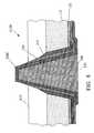
- Openings 130become exposed (see FIG. 4 A).
- Layers 210 and 310are removed at the bottoms of openings 130 but remain on the sidewalls.
- Layer 320is exposed on the wafer backside.
- layer 320covers the sidewalls of openings 130 , and each of layers 310 , 210 surrounds the layer 320 in the openings, as shown in the horizontal cross sectional view of FIG. 4 B.
- the bottom portion 320 C of layer 320provides a contact pad that can be bonded to a wiring substrate (e.g. a printed circuit board) or to another integrated circuit.
- a wiring substratee.g. a printed circuit board
- another integrated circuite.g. a printed circuit board
- contacts 320 Cmay serve as input, output, or input/output terminals carrying AC (alternating current) signals.
- Layer 210shields the substrate 110 from the electromagnetic field generated by these signals. The shielding reduces signal attenuation and substrate noise.
- Conductive shields 210can be held at a constant potential VREF, as schematically shown in FIG. 4 A. VREF can be ground, VCC, or some other value.
- Each conductive shield 210 in an opening 130physically contacts a surrounding region 110 . 1 of substrate 110 .
- Conductive shields 210 in different openings 130can be at different potentials in the same integrated circuit.
- Region 110 . 1can be at the same potential VREF as the adjacent shield 210 or at a different constant or variable potential. In some embodiments, the regions 210 , 110 . 1 form a diode reverse biased during operation.
- FIG. 4Aillustrates a region 110 . 2 in substrate 110 .
- Region 110 . 2can be a transistor region (source, drain, channel, emitter, etc.) or any other type of region.
- Region 110 . 2can carry an AC signal.
- Region 110 . 2is shielded by layer 210 from signals on pads 320 C.
- Region 110 . 2may be isolated from region 110 . 1 by one or more P-N junctions.
- the integrated circuitmay have other backside contacts (not shown) which do not have a conductive shield around them. These contacts can be manufactured from layer 320 at the same time as the shielded contacts 320 C.
- the non-shielded contactsare manufactured in openings (not shown) formed at the same time as openings 130 , but layer 210 is etched out of these openings when this layer is patterned.
- non-shielded contactscarry a DC voltage, e.g. they serve as power supply or ground terminals.
- non-shielded contactscarry low frequency signals. The invention is not limited to a particular use of shielded or non-shielded contacts.
- Conductive layers 210 , 320can be made of metals, doped polysilicon, conductive metal suicides, and their combinations.
- Insulating layers 120 , 310 , 340can be made of silicon dioxide, silicon nitride, silicon oxynitride, aluminum oxide, tantalum oxide, titanium oxide, and their combinations.
- Layers 210 , 320 , 120 , 310can be fabricated by known techniques, such as sputtering, thermal oxidation, or CVD (chemical vapor deposition). Other materials and fabrication techniques, known or to be invented, can also be used.
- Each of layers 210 , 320 , 120 , 310 , 340can include multiple layers and multiple materials.
- layer 210includes a layer that has a higher conductivity than the adjacent semiconductor regions 110 . 1 .
- the wafer thinningis a blanket etch process.
- the etchcontinues and etchs the substrate 110 and the layers 210 , 310 at the same time.
- insulator 310protrudes down after the etch from the backside surface of substrate 110 .
- the protruding insulatorhelps insulate the substrate from contact pads 320 C when the contact pads are bonded to a wiring substrate or another integrated circuit.
- Conductor 210also protrudes down from substrate 110 , but insulator 310 protrudes more to improve insulation between conductors 210 , 320 .
- This profileis achieved by choosing the materials and the etching process so that the etch rate of wafer 110 is higher than the etch rate of layer 210 and the etch rate of layer 210 is higher than the etch rate of insulator 310 .
- the layer 320has the lowest etch rate (zero for example).
- the etchis performed by fluorine containing plasma at atmospheric pressure.
- a suitable etcheris type Tru-Etch 3000 (Trademark) available from Tru-Si Technologies, Inc., of Sunnyvale, California.
- Wafer 110is made of monocrystalline silicon.
- Conductor 210is made of titanium, tungsten, molybdenum, vanadium, or their silicides, or titanium nitride, or a combination of these materials.
- Insulator 310is made of silicon dioxide, silicon nitride, silicon oxynitride, or a combinationof these materials.
- Conductor 320is formed, or includes a layer formed, of aluminum, copper, nickel, or a
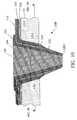
- FIG. 5illustrates another embodiment.
- the conductor 210is etched faster than substrate 110 and insulator 310 .
- the substrate 110can be monocrystalline silicon and the layer 210 can be doped polysilicon.
- the remaining materialscan be as in FIG. 4 A.
- Polysiliconis initially etched faster than monocrystalline silicon 110 , but when polysilicon becomes recessed relative to silicon 110 , the polysilicon etch rate may decrease if the recess is narrow, i.e. if the layer 210 is thin.
- each of layers 120 , 210 , 310 , 320is about 1 ⁇ m thick, and each opening 130 is about 100 ⁇ m deep and 30 to 50 ⁇ m wide.
- FIG. 5is advantages because it facilitates insulation of layer 210 on the wafer backside.
- the inventionis not limited to any etch rates or etching processes.
- layer 210is a highly doped conductive region of substrate 110 .
- Layer 210can be created by ion implantation or dopant diffusion before or after formation of openings 130 .
- layer 210can be formed when substrate 110 is created.
- layer 210can be an epitaxial layer in substrate 110 .
- Layer 210can also be formed by a combination of the techniques mentioned above (ion implantation, epitaxial layer, etc.).
- layer 210does not need to extend to the bottom of openings 130 because the bottoms of openings 130 are removed during wafer thinning.
- Layer 210may cover all or part of the sidewalls of the openings 130 after the structure has been thinned.
- the resistivity of layer 210is at most 100 ⁇ 10 ⁇ 6 ⁇ .cm, or at most 90 ⁇ 10 ⁇ 6 ⁇ .cm, or at most 50 ⁇ 10 ⁇ 6 ⁇ .cm, or at most 10 ⁇ 10 ⁇ 6 ⁇ .cm. These ranges are exemplary and not limiting.
- the wafer thinningincludes multiple stages. At first, wafer 110 is thinned by etching, mechanical grinding, and/or some other process. Conductor 210 becomes exposed at the bottom and possibly at the sides of openings 130 but conductor 210 does not have to be etched at this stage. Conductor 210 is etched at a later stage by a separate process. Substrate 110 and insulator 310 may be etched at this later stage and/or at a subsequent stage. Photolithographic masking can be used at any or all of these stages to obtain desired etch selectivity. Some embodiments do not use photolithographic masking.
- an insulator 602(FIG. 6) is formed on wafer backside 110 B.
- the portions of layer 602 on substrate 110 , conductor 210 , and conductor 320are marked respectively as 602 . 110 , 602 . 210 , 602 . 320 .
- insulator 602is formed by processing the wafer backside with oxygen or nitrogen to form oxygen or nitrogen compounds 602 . 110 , 602 . 210 , 602 . 320 (for example, silicon oxide or nitride and metal oxides or nitrides). Oxygen or nitrogen plasma processing can be used. Masking is not needed. Later, the insulator 602 .
- 320 on contacts 320 Ccan be removed without removing the insulators 602 . 110 , 602 . 210 .
- the insulator 602 . 320is removed without masking.
- the insulator 602 . 320is removed by a solder flux that does not attack the insulators 602 . 110 , 602 . 210 .
- layer 320is copper, or includes a copper sub-layer on the bottom; layer 210 is titanium; substrate 110 is silicon; and insulator 602 is formed with oxygen. Solder fluxes are known that will remove copper oxide but not silicon oxide or titanium oxide.
- substrate 110is made of an insulating material
- the insulator 602 . 110will not necessarily be formed.
- Insulator 610may or may not be formed on insulator 310 .
- insulator 602can be grown on substrate 110 but not on conductor 210 depending on the materials and processes used.
- FIGS. 7-8Another suitable process for insulating the wafer backside is illustrated in FIGS. 7-8.
- the structureis positioned with the backside 110 B facing up, and a flowable material 610 is deposited on the backside by a spin-on or spraying process.
- Suitable materialsinclude glass, polyimide, flowable thermosetting polymers, or other materials which can be deposited by a spin-on or spraying process and which are dielectric when cured. Low viscosity materials are particularly suitable but not necessary. See the aforementioned U.S. patent application Ser. No. 09/456,225.
- layer 610covers the contacts 320 C, but layer 610 is thinner over the contacts 320 C than over the rest of the wafer. In other embodiments, layer 610 does not cover the contacts 320 C.
- Layer 610is cured, and then etched bya blanket etch until the contacts 320 C are exposed. See FIG. 8 .
- Conductor 210remains covered by layer 610 . The etch can be omitted if layer 610 did not cover the contact 320 C when the layer 610 was initially deposited.
- the thickness of layer 610 over contacts 320 C at the stage of FIG. 7is about 1 to 10 ⁇ m; contacts 320 C protrude by about 5 to 50 ⁇ m (measured vertically) over the backside (top) surface of substrate 110 ; insulator 310 protrudes by about 1 to 40 ⁇ m; conductor 210 protrudes by about 3 to 30 ⁇ m.
- Insulator 602is formed as in FIG. 6, then insulator 610 is formed as in FIGS. 7-8. In other embodiments, insulator 610 is formed first. The etch of insulator 610 (FIG. 8) may or may not expose the conductor 210 . Then insulator 602 is grown to assure insulation of conductor 210 on the wafer backside.
- insulator 610can be formed from a flowable or non-flowable material, and patterned photolithographically to expose the contacts 320 C but not the conductor 210 or substrate 110 .
- FIGS. 9 and 10illustrate another thinning technique.
- a mechanical processsuch as mechanical grinding or chemical mechanical polishing exposes the conductor 320 on the backside 110 B.
- the mechanical processremoves the conductor 320 from the bottom of openings 130 , so that the filler 340 is exposed.
- a wet or dry etchis used to expose the conductor 320 , and then a mechanical process is used to remove conductor 320 from the bottom of openings 130 .
- Other combinations of processesare possible.
- the wafer backsideis flat because all of the materials are removed at the same rate, though this is not necessary.
- the wafer backsideis etched by a process which etches the materials 110 , 210 , 310 faster than the conductor 320 and the filler 340 (FIG. 10 ).
- the etching processes described above in connection with FIGS. 4A, 4 B, and 5can be used to achieve a profile similar to that of FIG. 4A or 5 .
- the wafer backsidecan be cleaned to remove any particles of materials 320 , 340 from the surface of substrate 110 .
- the particles of materials 320 , 340could be carried onto the back surface of substrate 110 by the mechanical process described above in connection with FIG. 9, especially if the materials 340 and 320 are soft (for example, copper).
- the filler 340can be omitted, or can be part of layer 320 .
- the wafer backsidecan be insulated by any of the processes described above in connection with FIGS. 6-8.
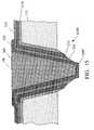
- FIGS. 11-13illustrate another thinning technique.
- the thinning operationremoves a portion of substrate 110 and conductor 210 , but the insulator 310 still covers the conductor 320 .
- Suitable processes for this operationinclude mechanical grinding of substrate 110 , followed by an atmospheric pressure etch in a fluorine containing plasma such as described above in connection with FIGS. 4A, 5 .
- insulator 310is silicon dioxide. Silicon dioxide can be etched about 8-10 times slower than monocrystalline silicon.
- insulator 310is aluminum oxide, titanium oxide, or Al x Ti y O z . These compounds can be wet-etched by known techniques. Other compounds, compositions, and processes are possible.
- insulator 610(FIG. 12) is fabricated as described above in connection with FIGS. 7-8. For example, a flowable material is spun or sprayed on the wafer backside, then cured, and then etched with a blanket etch. The etch is selective to insulator 310 so that the conductor 320 is not exposed.
- insulator 610is polyimide etched in oxygen plasma at atmospheric pressure in a Tru-Etch 3000 etcher; insulator 310 is silicon dioxide. Insulator 310 and conductor 320 protrude from the top surface of insulator 610 .
- insulator 310is etched off the contacts 320 C (FIG. 13 ). This etch does not remove the insulator 610 if insulator 610 is sufficiently thick and/or the etch is sufficiently selective to insulator 610 .
- insulator 610can be polyimide
- insulator 310can be silicon dioxide
- the etchcan be performed in a fluorine containing plasma (e.g., at atmospheric pressure in a Tru-Etch 3000 etcher).
- Photolithographycan also be used to achieved desired selectivity. Some embodiments do not use photolithography.
- fabrication of insulator 610is preceded, or followed, by fabrication of insulator 602 (FIG. 6 ).
- Insulator 602can be formed before or after the etch of insulator 310 (FIG. 13 ).
- the wafercan be diced to provide a number of individual integrated circuits.
- the whole wafercan be a single integrated circuit.
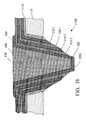
- FIG. 14illustrates another embodiment.
- an insulating layer 1110is fabricated over the wafer.
- conductive layer 210is fabricated that will provide electromagnetic shielding.
- Insulator 1110insulates the substrate 110 from conductor 210 .
- Suitable insulatorsinclude silicon dioxide, BPSG, silicon nitride, and other insulating materials, known or to be invented.
- the insulatorcan be formed by thermal oxidation, CVD (chemical vapor deposition), or other techniques, known or to be invented.
- Insulator 1110can be patterned as needed.
- Layers 210 , 310 , 320 , and optionally 340are formed as described above in connection with FIGS. 1-13.
- FIG. 15illustrates the structure thinned by an etch described above in connection with FIG. 4 A.
- Insulator 1110is etched off the conductor 210 on backside 110 B by this etch.
- the etch rate of insulator 1110is the same as for insulator 310 , though this is not necessary.
- the two insulatorscan be formed from identical materials.
- the remaining fabrication steps, including fabrication of insulators 602 , 610can be as described above in connection with FIGS. 1-13.
- insulator 1110is removed from some, but not all, of openings 130 .
- conductor 210contacts substrate 110 in some, but not all, of the openings.
- Layer 210can be patterned so that the shields 210 in different openings are insulated from each other.
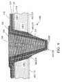
- Some embodimentsinclude multiple shield layers.
- two conductive shield layers 210 . 1 , 210 . 2are present.
- insulator 1110is fabricated as described above in connection with FIG. 14 . (Insulator 1110 is omitted in some embodiments, or is fabricated but etched out of some, but not all, of openings 130 .)
- conductive layer 210 . 1 , insulating layer 310 . 1 , conductive layer 210 . 2 , insulating layer 310 . 2 , and conductive layer 320are fabricated, in that order. These layers are patterned as desired. For example, layer 210 . 1 or 210 .
- each shield 210 . 1 , 210 . 2can be held at a constant potential, as described above in connection with FIG. 4 A. Multiple shield layers improve electromagnetic shielding.
- the wafer front sidecan be bonded to one or more substrates 1410 to form a vertically integrated structure.
- One or more of the substrates 1410may include circuitry. See the aforementioned U.S. patent application Ser. No. 09/456,225.
- a substrate 1410can be used for protection only. Substrates 1410 will protect the circuitry at the front side of wafer 110 during the thinning of wafer 110 and subsequent processing steps.
- FIG. 18illustrates a circuit diagram obtained in FIGS. 4A-13.
- Conductive layers 210 , 320 and insulator 310form a capacitor 1504 .
- the capacitorcan be used as a bandpath filter, for example.
- pad 320 Cis connected to a circuit 1510 formed in substrate 110 .
- pad 320is not connected to such a circuit, but conductor 210 is.
- both pad 320 C and conductor 210are connected to such circuits.
- Capacitor 1504can be a junction capacitor or a rectifier. Insulator 310 can be omitted. Layers 320 , 210 can be semiconductor layers of opposite conductivity types to form a P-N junction. Alternatively, the two layers can form a Schottky junction if one of the two layers is an N-type semiconductor layer and the other one of the two layers is a metal layer.
- diode 1610In each of FIGS. 19, 20 , conductor 210 and substrate 110 form a diode 1610 .
- Layer 210serves as the anode in FIG. 19, as the cathode in FIG. 20.
- Diode 1610is a P-N junction diode if conductor 210 and the adjacent region 110 . 1 of substrate 110 are semiconductor materials of opposite conductivity types.
- Diode 1610is a Schottky diode if layer 210 is metal and region 110 . 1 is N type.
- Pad 320 C, layer 210 , and/or substrate region 110 . 1can be connected to circuits formed in substrate 110 , such as circuit 1510 .
- FIG. 21is a circuit diagram for the structure of FIG. 15 .
- Capacitor 1504 . 1is formed like capacitor 1504 in FIG. 18 .
- Capacitor 1504 . 2is formed by conductor 210 , substrate region 110 . 1 , and insulator 1110 .
- Substrate region 110 . 1is doped to achieve desired conductivity.
- capacitors 1504 . 1 , 1504 . 2can be junction capacitors or rectifiers as described above in connection with FIGS. 18-20. Insulating layers 310 and/or 1110 can be omitted.
- FIG. 22is a circuit diagram for the structure of FIG. 16 .
- Capacitor 1504 . 1is formed by conductive layers 320 , 210 . 2 and insulator 310 . 2 .
- Capacitor 1504 . 2formed by conductive layers 210 . 2 , 210 . 1 and insulator 310 . 1 .
- Capacitor 1504 . 3is formed by layer 210 . 1 , substrate region 110 . 1 , and insulator 1110 .
- capacitors 1504 . 1 , 1504 . 2 , 1504 . 3can be junction capacitors or rectifiers.
- connection 1910can be made outside of the opening 130 .
- Connection 1910can be a permanent connection.
- connection 1910can be programmable (e.g. using a fuse or an antifuse), to allow the capacitance to be adjusted during or after manufacturing.
- Connection 1910can be realized by means of contact openings (not shown) etched outside of opening 130 and allowing the layers 320 , 210 . 1 to contact each other directly or through some other layer or layers.
- Any number of layers 210can be used to form any number of capacitors and rectifiers between contact pad 320 C and substrate 110 and to provide desired electromagnetic shielding. Connections 1910 can be used to obtain a desired network.
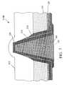
- FIG. 23Aillustrates another type of capacitor structure.
- the structureis manufactured as follows:
- One or more openings 130are formed in the front side of substrate 110 , as in FIGS. 1-17.
- insulating layer 1110is formed as in FIG. 16 .
- One or more conductive layers 210are formed in the openings as in FIG. 15 or 16 . Only one such layer is shown in FIG. 23 A. Insulating layers 310 (such as 310 . 1 , 310 . 2 in FIG. 16) can optionally be formed between layers 210 .
- insulator 310is formed in the opening over the layers 210 , using the same techniques as in FIG. 15 .
- Conductive layer 320 . 1is formed using techniques described above for layer 320 of FIG. 3-16.
- Insulating layer 2010 . 1is formed using techniques described above for layer 310 (FIG. 15 ).
- Step 5is repeated to form conductive layer 320 . 2
- step 6is repeated to form insulating layer 2010 . 2
- step 5is repeated to form conductive layer 320 . 3 .
- the openings 130are filled with some material 340 (as in FIG. 3 ).
- the openingscan also be filled at step 7 with layer 320 . 3 .
- the wafer backside 11 OBis processed to expose the layer 320 . 1 . This can be done by techniques described above in connection with FIGS. 4A-17.
- the exposed portion of layer 320 . 1provides contact pad 320 C.
- the wafer backsidecan be insulated as described above in connection with FIGS. 6-17.
- FIG. 23Bshows a circuit diagram for FIG. 23 A.
- Layers 320 . 1 , 310 , 210form a capacitor 1504 . 1 .
- Layers 210 , 1110 , and substrate region 110 . 1form a capacitor 1504 . 2 (if region 110 . 1 is made conductive by doping).
- Layers 320 . 1 , 2010 . 1 , 320 . 2form a capacitor 2020 . 1 .
- Layers 320 . 2 , 2010 . 2 , 320 . 3form a capacitor 2020 . 2 .
- Permanent or programmable connections 1910can be formed outside of openings 130 between selected conductive layers.
- a permanent connection 1910 . 1connects layer 320 . 2 to layer 210 .
- capacitors 2020 . 1 , 1504 . 1are connected in parallel between the pad 320 C and an electrical node N formed by layers 210 , 320 . 2 .
- a permanent connection 1910 . 2connects layer 320 . 3 to layer 320 . 1 , increasing the total capacitance between pad 320 C and node N.
- FIG. 23Cis another circuit representation of the structure of FIG. 23 A.
- Capacitors 2020 . 1 , 2020 . 2can be viewed as a single capacitor having: (i) one conductive plate having “fingers” 320 . 1 , 320 . 3 , and (ii) another conductive plate having “fingers” 210 , 320 . 2 .
- These interleaving fingersoverlay each other, forming an interdigitated structure as seen in the vertical cross section. This helps explain why a large capacitance can be obtained in a small area.
- Steps 5 and 6can be repeated to form any number of layers 320 , 2010 , and thus any number of capacitors 2020 .
- One or more of insulating layers 2010can be omitted, and one or more of the elements 2020 can be junction capacitors or rectifiers.
- Layer 310can be omitted and a junction capacitor or rectifier can be formed by layers 320 . 1 , 210 .
- any one or more of layers 1110 , 210 , 310 , 320 , 2010are present in some openings 130 but not in the other openings 130 in the same structure.
- some of these layerscan be etched out of some of the openings.
- these layerscan be formed selectively in some but not all of the openings.
- Layers 210provide electromagnetic shielding for substrate 110 .
- any number of layers 210 and any number of layers 320can be provided to obtain a large number of capacitive networks and a large variety of electromagnetic shielding parameters in a small area. Rectifiers or junction capacitors can be obtained if one or more of insulating layers 310 , 2010 , 1110 are omitted.
Landscapes
- Engineering & Computer Science (AREA)
- Physics & Mathematics (AREA)
- Power Engineering (AREA)
- General Physics & Mathematics (AREA)
- Computer Hardware Design (AREA)
- Microelectronics & Electronic Packaging (AREA)
- Condensed Matter Physics & Semiconductors (AREA)
- Manufacturing & Machinery (AREA)
- Health & Medical Sciences (AREA)
- Electromagnetism (AREA)
- Toxicology (AREA)
- Internal Circuitry In Semiconductor Integrated Circuit Devices (AREA)
- Electrodes Of Semiconductors (AREA)
- Semiconductor Integrated Circuits (AREA)
- Shielding Devices Or Components To Electric Or Magnetic Fields (AREA)
Abstract
Description
Claims (50)
Priority Applications (8)
| Application Number | Priority Date | Filing Date | Title |
|---|---|---|---|
| US09/792,311US6498381B2 (en) | 2001-02-22 | 2001-02-22 | Semiconductor structures having multiple conductive layers in an opening, and methods for fabricating same |
| US09/941,447US6844241B2 (en) | 2001-02-22 | 2001-08-28 | Fabrication of semiconductor structures having multiple conductive layers in an opening |
| JP2002576018AJP4063078B2 (en) | 2001-02-22 | 2002-02-20 | Semiconductor structure having a plurality of conductive layers formed in an opening, and a method for manufacturing the same |
| EP02739087AEP1386355A2 (en) | 2001-02-22 | 2002-02-20 | Semiconductor chip having multiple conductive layers in an opening, and method for fabricating same |
| PCT/US2002/005371WO2002078087A2 (en) | 2001-02-22 | 2002-02-20 | Semiconductor chip having multiple conductive layers in an opening, and method for fabricating same |
| AU2002311762AAU2002311762A1 (en) | 2001-02-22 | 2002-02-20 | Semiconductor chip having multiple conductive layers in an opening, and method for fabricating same |
| KR10-2003-7010999AKR100509898B1 (en) | 2001-02-22 | 2002-02-20 | Semiconductor structures having multiple conductive layers in an opening, and methods for fabricating same |
| US11/014,464US7001825B2 (en) | 2001-02-22 | 2004-12-16 | Semiconductor structures having multiple conductive layers in an opening, and methods for fabricating same |
Applications Claiming Priority (1)
| Application Number | Priority Date | Filing Date | Title |
|---|---|---|---|
| US09/792,311US6498381B2 (en) | 2001-02-22 | 2001-02-22 | Semiconductor structures having multiple conductive layers in an opening, and methods for fabricating same |
Related Child Applications (1)
| Application Number | Title | Priority Date | Filing Date |
|---|---|---|---|
| US09/941,447DivisionUS6844241B2 (en) | 2001-02-22 | 2001-08-28 | Fabrication of semiconductor structures having multiple conductive layers in an opening |
Publications (2)
| Publication Number | Publication Date |
|---|---|
| US20020115290A1 US20020115290A1 (en) | 2002-08-22 |
| US6498381B2true US6498381B2 (en) | 2002-12-24 |
Family
ID=25156458
Family Applications (3)
| Application Number | Title | Priority Date | Filing Date |
|---|---|---|---|
| US09/792,311Expired - LifetimeUS6498381B2 (en) | 2001-02-22 | 2001-02-22 | Semiconductor structures having multiple conductive layers in an opening, and methods for fabricating same |
| US09/941,447Expired - LifetimeUS6844241B2 (en) | 2001-02-22 | 2001-08-28 | Fabrication of semiconductor structures having multiple conductive layers in an opening |
| US11/014,464Expired - LifetimeUS7001825B2 (en) | 2001-02-22 | 2004-12-16 | Semiconductor structures having multiple conductive layers in an opening, and methods for fabricating same |
Family Applications After (2)
| Application Number | Title | Priority Date | Filing Date |
|---|---|---|---|
| US09/941,447Expired - LifetimeUS6844241B2 (en) | 2001-02-22 | 2001-08-28 | Fabrication of semiconductor structures having multiple conductive layers in an opening |
| US11/014,464Expired - LifetimeUS7001825B2 (en) | 2001-02-22 | 2004-12-16 | Semiconductor structures having multiple conductive layers in an opening, and methods for fabricating same |
Country Status (6)
| Country | Link |
|---|---|
| US (3) | US6498381B2 (en) |
| EP (1) | EP1386355A2 (en) |
| JP (1) | JP4063078B2 (en) |
| KR (1) | KR100509898B1 (en) |
| AU (1) | AU2002311762A1 (en) |
| WO (1) | WO2002078087A2 (en) |
Cited By (81)
| Publication number | Priority date | Publication date | Assignee | Title |
|---|---|---|---|---|
| US20020171138A1 (en)* | 2001-05-21 | 2002-11-21 | Yasuo Osone | Multilayer wiring board and semiconductor device |
| US20030057544A1 (en)* | 2001-09-13 | 2003-03-27 | Nathan Richard J. | Integrated assembly protocol |
| US20030153119A1 (en)* | 2002-02-14 | 2003-08-14 | Nathan Richard J. | Integrated circuit package and method for fabrication |
| US20030151132A1 (en)* | 2002-02-14 | 2003-08-14 | Crippen Warren Stuart | Microelectronic die providing improved heat dissipation, and method of packaging same |
| US20030183920A1 (en)* | 2002-03-28 | 2003-10-02 | Goodrich Joel Lee | Hermetic electric component package |
| US20030200654A1 (en)* | 2002-04-25 | 2003-10-30 | Fujitsu Limited | Method of manufacturing electronic circuit component |
| US20040115919A1 (en)* | 2001-05-14 | 2004-06-17 | Yuji Takaoka | Semiconductor device and its manufacturing method |
| US20040142574A1 (en)* | 2002-03-19 | 2004-07-22 | Seiko Epson Corporation | Semiconductor device and method of manufacturing the same, circuit board, and electronic instrument |
| US20040161926A1 (en)* | 2003-01-24 | 2004-08-19 | Seiko Epson Corporation | Method for manufacturing semiconductor device, and method for manufacturing semiconductor module |
| US20050064707A1 (en)* | 2003-09-23 | 2005-03-24 | Nishant Sinha | Process and integration scheme for fabricating conductive components, through-vias and semiconductor components including conductive through-wafer vias |
| US20050067688A1 (en)* | 2003-09-26 | 2005-03-31 | Tessera, Inc. | Structure and method of making capped chips including vertical interconnects having stud bumps engaged to surfaces of said caps |
| US20050116344A1 (en)* | 2003-10-29 | 2005-06-02 | Tessera, Inc. | Microelectronic element having trace formed after bond layer |
| US20050136634A1 (en)* | 2003-12-17 | 2005-06-23 | Sergey Savastiouk | Integrated circuits and packaging substrates with cavities, and attachment methods including insertion of protruding contact pads into cavities |
| US20050133930A1 (en)* | 2003-12-17 | 2005-06-23 | Sergey Savastisuk | Packaging substrates for integrated circuits and soldering methods |
| US20050230805A1 (en)* | 2004-04-16 | 2005-10-20 | Ikuya Miyazawa | Semiconductor device, method for producing the same, circuit board, and electronic apparatus |
| US20060043598A1 (en)* | 2004-08-31 | 2006-03-02 | Kirby Kyle K | Methods of manufacture of a via structure comprising a plurality of conductive elements, semiconductor die, multichip module, and system including same |
| US20060071281A1 (en)* | 2004-09-28 | 2006-04-06 | Simon Dodd | Integrated circuit and method for manufacturing |
| US20060183270A1 (en)* | 2005-02-14 | 2006-08-17 | Tessera, Inc. | Tools and methods for forming conductive bumps on microelectronic elements |
| US7098518B1 (en) | 2003-08-27 | 2006-08-29 | National Semiconductor Corporation | Die-level opto-electronic device and method of making same |
| US20060246621A1 (en)* | 2002-02-14 | 2006-11-02 | Intel Corporation | Microelectronic die including thermally conductive structure in a substrate thereof and method of forming same |
| US20060254808A1 (en)* | 2004-01-12 | 2006-11-16 | Farnworth Warren M | Substrate precursor structures |
| US20070138644A1 (en)* | 2005-12-15 | 2007-06-21 | Tessera, Inc. | Structure and method of making capped chip having discrete article assembled into vertical interconnect |
| US20070187142A1 (en)* | 2002-11-07 | 2007-08-16 | Fujikura Ltd. | Method for fabricating a through-hole interconnection substrate and a through-hole interconnection substrate |
| US20070194431A1 (en)* | 2006-02-20 | 2007-08-23 | Corisis David J | Conductive vias having two or more conductive elements for providing electrical communication between traces in different planes in a substrate, semiconductor device assemblies including such vias, and accompanying methods |
| US7265440B2 (en) | 2003-06-16 | 2007-09-04 | Tessera Technologies Hungary Kft. | Methods and apparatus for packaging integrated circuit devices |
| US20080083977A1 (en)* | 2006-10-10 | 2008-04-10 | Tessera, Inc. | Edge connect wafer level stacking |
| US20080083976A1 (en)* | 2006-10-10 | 2008-04-10 | Tessera, Inc. | Edge connect wafer level stacking |
| US20080116544A1 (en)* | 2006-11-22 | 2008-05-22 | Tessera, Inc. | Packaged semiconductor chips with array |
| US20080157323A1 (en)* | 2006-12-28 | 2008-07-03 | Tessera, Inc. | Stacked packages |
| US20080173993A1 (en)* | 2007-01-18 | 2008-07-24 | International Business Machines Corporation | Chip carrier substrate capacitor and method for fabrication thereof |
| US20080295329A1 (en)* | 2007-05-30 | 2008-12-04 | Sriram Muthukumar | Multi-chip packaging using an interposer such as a silicon based interposer with through-silicon-vias |
| US20080295325A1 (en)* | 2007-05-30 | 2008-12-04 | Sriram Muthukumar | Multi-chip packaging using an interposer such as a silicon based interposer with through-silicon-vias |
| US7479398B2 (en) | 2003-07-03 | 2009-01-20 | Tessera Technologies Hungary Kft. | Methods and apparatus for packaging integrated circuit devices |
| US20090039528A1 (en)* | 2007-08-09 | 2009-02-12 | Tessera, Inc. | Wafer level stacked packages with individual chip selection |
| US20090126983A1 (en)* | 2007-11-19 | 2009-05-21 | Harvey Paul M | Method and Apparatus to Reduce Impedance Discontinuity in Packages |
| US20090160065A1 (en)* | 2006-10-10 | 2009-06-25 | Tessera, Inc. | Reconstituted Wafer Level Stacking |
| US7566955B2 (en) | 2001-08-28 | 2009-07-28 | Tessera, Inc. | High-frequency chip packages |
| US20090188707A1 (en)* | 2008-01-30 | 2009-07-30 | Van Den Hoek Willibrordus Gerardus Maria | Method and Apparatus for Manufacture of Via Disk |
| US20090212438A1 (en)* | 2008-02-26 | 2009-08-27 | Franz Kreupl | Integrated circuit device comprising conductive vias and method of making the same |
| US20090278238A1 (en)* | 2008-05-12 | 2009-11-12 | Texas Instruments Inc | Tsvs having chemically exposed tsv tips for integrated circuit devices |
| US20090316378A1 (en)* | 2008-06-16 | 2009-12-24 | Tessera Research Llc | Wafer level edge stacking |
| US20100140805A1 (en)* | 2008-12-10 | 2010-06-10 | Hung-Pin Chang | Bump Structure for Stacked Dies |
| US20100171197A1 (en)* | 2009-01-05 | 2010-07-08 | Hung-Pin Chang | Isolation Structure for Stacked Dies |
| US20100230795A1 (en)* | 2009-03-13 | 2010-09-16 | Tessera Technologies Hungary Kft. | Stacked microelectronic assemblies having vias extending through bond pads |
| US20100270679A1 (en)* | 2006-10-17 | 2010-10-28 | Tessera, Inc. | Microelectronic packages fabricated at the wafer level and methods therefor |
| US20100276786A1 (en)* | 2009-04-29 | 2010-11-04 | International Business Machines Corporation | Through Substrate Vias |
| US20110006432A1 (en)* | 2007-07-27 | 2011-01-13 | Tessera, Inc. | Reconstituted wafer stack packaging with after-applied pad extensions |
| US20110012259A1 (en)* | 2006-11-22 | 2011-01-20 | Tessera, Inc. | Packaged semiconductor chips |
| US7936062B2 (en) | 2006-01-23 | 2011-05-03 | Tessera Technologies Ireland Limited | Wafer level chip packaging |
| US20110101541A1 (en)* | 2005-09-29 | 2011-05-05 | Renesas Electronics Corporation | Semiconductor device |
| US20110147901A1 (en)* | 2009-12-17 | 2011-06-23 | Rui Huang | Integrated circuit packaging system with package stacking and method of manufacture thereof |
| US20110193241A1 (en)* | 2010-02-09 | 2011-08-11 | Yu-Lin Yen | Chip package and method for forming the same |
| KR101108947B1 (en)* | 2010-12-09 | 2012-02-08 | 테세라, 인코포레이티드 | High Density 3D Integrated Capacitors |
| US8143095B2 (en) | 2005-03-22 | 2012-03-27 | Tessera, Inc. | Sequential fabrication of vertical conductive interconnects in capped chips |
| US20120146238A1 (en)* | 2007-07-16 | 2012-06-14 | Chao-Yuan Su | Method for Packaging Semiconductor Dies Having Through-Silicon Vias |
| US20120175784A1 (en)* | 2008-12-08 | 2012-07-12 | Stats Chippac, Ltd. | Semiconductor Device and Method of Forming Vertical Interconnect Structure in Substrate for IPD and Baseband Circuit Separated by High-Resistivity Molding Compound |
| US20120217987A1 (en)* | 2011-02-24 | 2012-08-30 | International Business Machines Corporation | Non-destructive determination of the moisture content in an electronic circuit board using comparison of capacitance measurements acquired from test coupons, and design structure/process therefor |
| US20130015440A1 (en)* | 2011-07-11 | 2013-01-17 | International Business Machines Corporation | Integrated circuit (ic) test probe |
| US8466059B2 (en) | 2010-03-30 | 2013-06-18 | Taiwan Semiconductor Manufacturing Company, Ltd. | Multi-layer interconnect structure for stacked dies |
| US8551815B2 (en) | 2007-08-03 | 2013-10-08 | Tessera, Inc. | Stack packages using reconstituted wafers |
| US8587126B2 (en) | 2010-12-02 | 2013-11-19 | Tessera, Inc. | Stacked microelectronic assembly with TSVs formed in stages with plural active chips |
| US8604605B2 (en) | 2007-01-05 | 2013-12-10 | Invensas Corp. | Microelectronic assembly with multi-layer support structure |
| US8610259B2 (en) | 2010-09-17 | 2013-12-17 | Tessera, Inc. | Multi-function and shielded 3D interconnects |
| US8610264B2 (en) | 2010-12-08 | 2013-12-17 | Tessera, Inc. | Compliant interconnects in wafers |
| US8637968B2 (en) | 2010-12-02 | 2014-01-28 | Tessera, Inc. | Stacked microelectronic assembly having interposer connecting active chips |
| US8735205B2 (en) | 2007-03-05 | 2014-05-27 | Invensas Corporation | Chips having rear contacts connected by through vias to front contacts |
| US8735287B2 (en) | 2007-07-31 | 2014-05-27 | Invensas Corp. | Semiconductor packaging process using through silicon vias |
| US8736066B2 (en) | 2010-12-02 | 2014-05-27 | Tessera, Inc. | Stacked microelectronic assemby with TSVS formed in stages and carrier above chip |
| US8742591B2 (en) | 2011-12-21 | 2014-06-03 | Stats Chippac, Ltd. | Semiconductor device and method of forming insulating layer in notches around conductive TSV for stress relief |
| US8791575B2 (en) | 2010-07-23 | 2014-07-29 | Tessera, Inc. | Microelectronic elements having metallic pads overlying vias |
| US8791549B2 (en) | 2009-09-22 | 2014-07-29 | Taiwan Semiconductor Manufacturing Company, Ltd. | Wafer backside interconnect structure connected to TSVs |
| US8796135B2 (en) | 2010-07-23 | 2014-08-05 | Tessera, Inc. | Microelectronic elements with rear contacts connected with via first or via middle structures |
| US8847380B2 (en) | 2010-09-17 | 2014-09-30 | Tessera, Inc. | Staged via formation from both sides of chip |
| US8900994B2 (en) | 2011-06-09 | 2014-12-02 | Taiwan Semiconductor Manufacturing Company, Ltd. | Method for producing a protective structure |
| US20150050792A1 (en)* | 2013-08-13 | 2015-02-19 | Globalfoundries Inc. | Extra narrow diffusion break for 3d finfet technologies |
| US9397038B1 (en) | 2015-02-27 | 2016-07-19 | Invensas Corporation | Microelectronic components with features wrapping around protrusions of conductive vias protruding from through-holes passing through substrates |
| US9412806B2 (en) | 2014-06-13 | 2016-08-09 | Invensas Corporation | Making multilayer 3D capacitors using arrays of upstanding rods or ridges |
| US9640437B2 (en) | 2010-07-23 | 2017-05-02 | Tessera, Inc. | Methods of forming semiconductor elements using micro-abrasive particle stream |
| US9748106B2 (en)* | 2016-01-21 | 2017-08-29 | Micron Technology, Inc. | Method for fabricating semiconductor package |
| US20170323828A1 (en)* | 2005-09-01 | 2017-11-09 | Micron Technology, Inc. | Microfeature workpieces and methods for forming interconnects in microfeature workpieces |
| US10790426B2 (en)* | 2016-04-01 | 2020-09-29 | Nichia Corporation | Method of manufacturing light emitting element mounting base member, method of manufacturing light emitting device using the light emitting element mounting base member, light emitting element mounting base member, and light emitting device using the light emitting element mounting base member |
Families Citing this family (55)
| Publication number | Priority date | Publication date | Assignee | Title |
|---|---|---|---|---|
| US20020163072A1 (en)* | 2001-05-01 | 2002-11-07 | Subhash Gupta | Method for bonding wafers to produce stacked integrated circuits |
| DE10241086B4 (en)* | 2001-09-06 | 2016-02-18 | Fuji Electric Co., Ltd | Composite integrated semiconductor device |
| US7948725B2 (en)* | 2001-09-06 | 2011-05-24 | Fuji Electric Systems Co., Ltd. | Composite integrated semiconductor device |
| JP2003273155A (en)* | 2002-03-18 | 2003-09-26 | Fujitsu Ltd | Semiconductor device and manufacturing method thereof |
| JP2004297019A (en)* | 2003-03-28 | 2004-10-21 | Seiko Epson Corp | Semiconductor device, circuit board and electronic equipment |
| US6897148B2 (en) | 2003-04-09 | 2005-05-24 | Tru-Si Technologies, Inc. | Electroplating and electroless plating of conductive materials into openings, and structures obtained thereby |
| US7101792B2 (en)* | 2003-10-09 | 2006-09-05 | Micron Technology, Inc. | Methods of plating via interconnects |
| WO2005059961A2 (en)* | 2003-12-10 | 2005-06-30 | The Regents Of The University Of California | Low crosstalk substrate for mixed-signal integrated circuits |
| US7012017B2 (en)* | 2004-01-29 | 2006-03-14 | 3M Innovative Properties Company | Partially etched dielectric film with conductive features |
| US7282932B2 (en)* | 2004-03-02 | 2007-10-16 | Micron Technology, Inc. | Compliant contact pin assembly, card system and methods thereof |
| JP2006019455A (en) | 2004-06-30 | 2006-01-19 | Nec Electronics Corp | Semiconductor device and manufacturing method thereof |
| JP2006024654A (en)* | 2004-07-06 | 2006-01-26 | Tokyo Electron Ltd | Interposer |
| JP2006024653A (en)* | 2004-07-06 | 2006-01-26 | Tokyo Electron Ltd | Through substrate and manufacturing method thereof |
| KR100858075B1 (en) | 2004-07-06 | 2008-09-11 | 도쿄엘렉트론가부시키가이샤 | Interposer |
| US7791141B2 (en)* | 2004-07-09 | 2010-09-07 | International Business Machines Corporation | Field-enhanced programmable resistance memory cell |
| US7109068B2 (en)* | 2004-08-31 | 2006-09-19 | Micron Technology, Inc. | Through-substrate interconnect fabrication methods |
| WO2006025210A1 (en)* | 2004-08-31 | 2006-03-09 | Matsushita Electric Industrial Co., Ltd. | Micromachine device |
| EP1691383A1 (en)* | 2005-02-14 | 2006-08-16 | TDK Corporation | Capacitor, method of making the same, filter using the same, and dielectric thin film used for the same |
| US20090117336A1 (en)* | 2005-06-01 | 2009-05-07 | Matsushita Electric Industrial Co., Ltd | Circuit board, method for manufacturing such circuit board, and electronic component using such circuit board |
| US7429529B2 (en)* | 2005-08-05 | 2008-09-30 | Farnworth Warren M | Methods of forming through-wafer interconnects and structures resulting therefrom |
| WO2007023950A1 (en)* | 2005-08-26 | 2007-03-01 | Hitachi, Ltd. | Semiconductor device manufacturing method |
| US7517798B2 (en)* | 2005-09-01 | 2009-04-14 | Micron Technology, Inc. | Methods for forming through-wafer interconnects and structures resulting therefrom |
| US8153464B2 (en)* | 2005-10-18 | 2012-04-10 | International Rectifier Corporation | Wafer singulation process |
| WO2007092770A2 (en)* | 2006-02-02 | 2007-08-16 | William Marsh Rice University | Fabrication de dispositifs electriques par façonnage de nanotubes |
| TW200737506A (en)* | 2006-03-07 | 2007-10-01 | Sanyo Electric Co | Semiconductor device and manufacturing method of the same |
| JP2007294652A (en)* | 2006-04-25 | 2007-11-08 | Matsushita Electric Ind Co Ltd | Semiconductor integrated circuit device and manufacturing method thereof |
| JP5258567B2 (en)* | 2006-08-11 | 2013-08-07 | セミコンダクター・コンポーネンツ・インダストリーズ・リミテッド・ライアビリティ・カンパニー | Semiconductor device and manufacturing method thereof |
| JP5010247B2 (en)* | 2006-11-20 | 2012-08-29 | オンセミコンダクター・トレーディング・リミテッド | Semiconductor device and manufacturing method thereof |
| US20080136038A1 (en)* | 2006-12-06 | 2008-06-12 | Sergey Savastiouk | Integrated circuits with conductive features in through holes passing through other conductive features and through a semiconductor substrate |
| TW200836322A (en)* | 2007-02-16 | 2008-09-01 | Touch Micro System Tech | Method of fabricating micro connectors |
| KR100843240B1 (en)* | 2007-03-23 | 2008-07-03 | 삼성전자주식회사 | A method of forming a through electrode of a semiconductor device for a wafer level stack and a semiconductor device for a wafer level stack |
| JP4961617B2 (en)* | 2007-10-01 | 2012-06-27 | 新光電気工業株式会社 | WIRING BOARD, MANUFACTURING METHOD THEREOF, AND SEMICONDUCTOR DEVICE |
| EP2081224A1 (en)* | 2007-12-27 | 2009-07-22 | Interuniversitaire Microelectronica Centrum vzw ( IMEC) | Maskless method of preparing metal contacts in a semiconductor substrate for bonding |
| US9324611B2 (en)* | 2008-04-03 | 2016-04-26 | Micron Technology, Inc. | Corrosion resistant via connections in semiconductor substrates and methods of making same |
| JP2010040862A (en)* | 2008-08-06 | 2010-02-18 | Fujikura Ltd | Semiconductor device |
| IT1391239B1 (en)* | 2008-08-08 | 2011-12-01 | Milano Politecnico | METHOD FOR BUMP FORMATION IN SUBSTRATES WITH THROUGH VIA |
| US8080862B2 (en)* | 2008-09-09 | 2011-12-20 | Qualcomm Incorporate | Systems and methods for enabling ESD protection on 3-D stacked devices |
| US8093151B2 (en)* | 2009-03-13 | 2012-01-10 | Stats Chippac, Ltd. | Semiconductor die and method of forming noise absorbing regions between THVS in peripheral region of the die |
| US8294240B2 (en)* | 2009-06-08 | 2012-10-23 | Qualcomm Incorporated | Through silicon via with embedded decoupling capacitor |
| US8558345B2 (en)* | 2009-11-09 | 2013-10-15 | International Business Machines Corporation | Integrated decoupling capacitor employing conductive through-substrate vias |
| US9299664B2 (en)* | 2010-01-18 | 2016-03-29 | Semiconductor Components Industries, Llc | Method of forming an EM protected semiconductor die |
| JP5609144B2 (en)* | 2010-02-19 | 2014-10-22 | ソニー株式会社 | Semiconductor device and through electrode test method |
| JP5115573B2 (en)* | 2010-03-03 | 2013-01-09 | オムロン株式会社 | Method for manufacturing connection pad |
| US8492878B2 (en)* | 2010-07-21 | 2013-07-23 | International Business Machines Corporation | Metal-contamination-free through-substrate via structure |
| US8742541B2 (en) | 2010-12-09 | 2014-06-03 | Tessera, Inc. | High density three-dimensional integrated capacitors |
| DE102011104305A1 (en) | 2011-06-16 | 2012-12-20 | Austriamicrosystems Ag | Production method for a semiconductor component with a conductor layer in the semiconductor body and semiconductor component |
| US9323010B2 (en) | 2012-01-10 | 2016-04-26 | Invensas Corporation | Structures formed using monocrystalline silicon and/or other materials for optical and other applications |
| US8757897B2 (en) | 2012-01-10 | 2014-06-24 | Invensas Corporation | Optical interposer |
| JP5880283B2 (en)* | 2012-05-29 | 2016-03-08 | 富士通セミコンダクター株式会社 | Manufacturing method of semiconductor device |
| US8940637B2 (en)* | 2012-07-05 | 2015-01-27 | Globalfoundries Singapore Pte. Ltd. | Method for forming through silicon via with wafer backside protection |
| EP2688092A1 (en)* | 2012-07-19 | 2014-01-22 | Ipdia | Semiconductor die with a through silicon via and corresponding manufacturing process |
| JP5954058B2 (en)* | 2012-09-04 | 2016-07-20 | 株式会社デンソー | Electronic equipment |
| JP6286169B2 (en)* | 2013-09-26 | 2018-02-28 | 新光電気工業株式会社 | Wiring board and manufacturing method thereof |
| JP7160594B2 (en)* | 2018-08-09 | 2022-10-25 | 太陽誘電株式会社 | Capacitor |
| EP4614572A1 (en)* | 2022-11-04 | 2025-09-10 | Sony Semiconductor Solutions Corporation | Electronic device |
Citations (16)
| Publication number | Priority date | Publication date | Assignee | Title |
|---|---|---|---|---|
| US4353082A (en)* | 1977-07-29 | 1982-10-05 | Texas Instruments Incorporated | Buried sense line V-groove MOS random access memory |
| US4580331A (en)* | 1981-07-01 | 1986-04-08 | Rockwell International Corporation | PNP-type lateral transistor with minimal substrate operation interference and method for producing same |
| US4694561A (en)* | 1984-11-30 | 1987-09-22 | American Telephone And Telegraph Company, At&T Bell Laboratories | Method of making high-performance trench capacitors for DRAM cells |
| US4810669A (en)* | 1987-07-07 | 1989-03-07 | Oki Electric Industry Co., Ltd. | Method of fabricating a semiconductor device |
| US5016068A (en)* | 1988-04-15 | 1991-05-14 | Texas Instruments Incorporated | Vertical floating-gate transistor |
| US5079615A (en)* | 1985-09-21 | 1992-01-07 | Semiconductor Energy Laboratory Co., Ltd. | Capacitor for a semiconductor |
| US5094972A (en)* | 1990-06-14 | 1992-03-10 | National Semiconductor Corp. | Means of planarizing integrated circuits with fully recessed isolation dielectric |
| US5317432A (en)* | 1991-09-04 | 1994-05-31 | Sony Corporation | Liquid crystal display device with a capacitor and a thin film transistor in a trench for each pixel |
| US5385861A (en)* | 1994-03-15 | 1995-01-31 | National Semiconductor Corporation | Planarized trench and field oxide and poly isolation scheme |
| WO1998019337A1 (en) | 1996-10-29 | 1998-05-07 | Trusi Technologies, Llc | Integrated circuits and methods for their fabrication |
| US5804478A (en) | 1991-05-17 | 1998-09-08 | Texas Instruments Incorporated | Method of forming a trench-type semiconductor memory device |
| US5843844A (en)* | 1995-01-25 | 1998-12-01 | Matsushita Electric Industrial Co., Ltd. | Probe sheet and method of manufacturing the same |
| US5854501A (en)* | 1995-11-20 | 1998-12-29 | Micron Technology, Inc. | Floating gate semiconductor device having a portion formed with a recess |
| US6016012A (en)* | 1996-11-05 | 2000-01-18 | Cypress Semiconductor Corporation | Thin liner layer providing reduced via resistance |
| US6221751B1 (en) | 1997-01-24 | 2001-04-24 | Chipscale, Inc. | Wafer fabrication of die-bottom contacts for electronic devices |
| US6322903B1 (en) | 1999-12-06 | 2001-11-27 | Tru-Si Technologies, Inc. | Package of integrated circuits and vertical integration |
Family Cites Families (24)
| Publication number | Priority date | Publication date | Assignee | Title |
|---|---|---|---|---|
| NL131898C (en)* | 1965-03-26 | |||
| US3508980A (en)* | 1967-07-26 | 1970-04-28 | Motorola Inc | Method of fabricating an integrated circuit structure with dielectric isolation |
| JPS5120267B2 (en)* | 1972-05-13 | 1976-06-23 | ||
| US4581814A (en)* | 1984-12-13 | 1986-04-15 | At&T Bell Laboratories | Process for fabricating dielectrically isolated devices utilizing heating of the polycrystalline support layer to prevent substrate deformation |
| US5246877A (en)* | 1989-01-31 | 1993-09-21 | Mitsubishi Denki Kabushiki Kaisha | Method of manufacturing a semiconductor device having a polycrystalline electrode region |
| US5229647A (en)* | 1991-03-27 | 1993-07-20 | Micron Technology, Inc. | High density data storage using stacked wafers |
| US5270261A (en)* | 1991-09-13 | 1993-12-14 | International Business Machines Corporation | Three dimensional multichip package methods of fabrication |
| US5332469A (en)* | 1992-11-12 | 1994-07-26 | Ford Motor Company | Capacitive surface micromachined differential pressure sensor |
| US5447871A (en)* | 1993-03-05 | 1995-09-05 | Goldstein; Edward F. | Electrically conductive interconnection through a body of semiconductor material |
| US5484745A (en)* | 1993-10-26 | 1996-01-16 | Yazaki Meter Co., Ltd. | Method for forming a semiconductor sensor |
| US6002177A (en)* | 1995-12-27 | 1999-12-14 | International Business Machines Corporation | High density integrated circuit packaging with chip stacking and via interconnections |
| US5747358A (en)* | 1996-05-29 | 1998-05-05 | W. L. Gore & Associates, Inc. | Method of forming raised metallic contacts on electrical circuits |
| SE9700141D0 (en)* | 1997-01-20 | 1997-01-20 | Abb Research Ltd | A schottky diode of SiC and a method of production thereof |
| US5949030A (en)* | 1997-11-14 | 1999-09-07 | International Business Machines Corporation | Vias and method for making the same in organic board and chip carriers |
| US6027956A (en)* | 1998-02-05 | 2000-02-22 | Integration Associates, Inc. | Process for producing planar dielectrically isolated high speed pin photodiode |
| US6122187A (en)* | 1998-11-23 | 2000-09-19 | Micron Technology, Inc. | Stacked integrated circuits |
| JP3991300B2 (en)* | 2000-04-28 | 2007-10-17 | 株式会社Sumco | Manufacturing method of bonded dielectric isolation wafer |
| US6500717B2 (en)* | 2000-12-01 | 2002-12-31 | Agere Systems Inc. | Method for making an integrated circuit device with dielectrically isolated tubs and related circuit |
| US6794272B2 (en)* | 2001-10-26 | 2004-09-21 | Ifire Technologies, Inc. | Wafer thinning using magnetic mirror plasma |
| US20030082847A1 (en)* | 2001-10-26 | 2003-05-01 | I-Fire Technologies, Inc. | Method and apparatus for wafer thinning |
| US6677235B1 (en)* | 2001-12-03 | 2004-01-13 | National Semiconductor Corporation | Silicon die with metal feed through structure |
| US6642081B1 (en)* | 2002-04-11 | 2003-11-04 | Robert Patti | Interlocking conductor method for bonding wafers to produce stacked integrated circuits |
| JP2004228392A (en)* | 2003-01-24 | 2004-08-12 | Seiko Epson Corp | Method of manufacturing semiconductor device and method of manufacturing semiconductor module |
| JP3990347B2 (en)* | 2003-12-04 | 2007-10-10 | ローム株式会社 | Semiconductor chip, manufacturing method thereof, and semiconductor device |
- 2001
- 2001-02-22USUS09/792,311patent/US6498381B2/ennot_activeExpired - Lifetime
- 2001-08-28USUS09/941,447patent/US6844241B2/ennot_activeExpired - Lifetime
- 2002
- 2002-02-20KRKR10-2003-7010999Apatent/KR100509898B1/ennot_activeExpired - Fee Related
- 2002-02-20JPJP2002576018Apatent/JP4063078B2/ennot_activeExpired - Fee Related
- 2002-02-20WOPCT/US2002/005371patent/WO2002078087A2/enactiveIP Right Grant
- 2002-02-20AUAU2002311762Apatent/AU2002311762A1/ennot_activeAbandoned
- 2002-02-20EPEP02739087Apatent/EP1386355A2/ennot_activeWithdrawn
- 2004
- 2004-12-16USUS11/014,464patent/US7001825B2/ennot_activeExpired - Lifetime
Patent Citations (16)
| Publication number | Priority date | Publication date | Assignee | Title |
|---|---|---|---|---|
| US4353082A (en)* | 1977-07-29 | 1982-10-05 | Texas Instruments Incorporated | Buried sense line V-groove MOS random access memory |
| US4580331A (en)* | 1981-07-01 | 1986-04-08 | Rockwell International Corporation | PNP-type lateral transistor with minimal substrate operation interference and method for producing same |
| US4694561A (en)* | 1984-11-30 | 1987-09-22 | American Telephone And Telegraph Company, At&T Bell Laboratories | Method of making high-performance trench capacitors for DRAM cells |
| US5079615A (en)* | 1985-09-21 | 1992-01-07 | Semiconductor Energy Laboratory Co., Ltd. | Capacitor for a semiconductor |
| US4810669A (en)* | 1987-07-07 | 1989-03-07 | Oki Electric Industry Co., Ltd. | Method of fabricating a semiconductor device |
| US5016068A (en)* | 1988-04-15 | 1991-05-14 | Texas Instruments Incorporated | Vertical floating-gate transistor |
| US5094972A (en)* | 1990-06-14 | 1992-03-10 | National Semiconductor Corp. | Means of planarizing integrated circuits with fully recessed isolation dielectric |
| US5804478A (en) | 1991-05-17 | 1998-09-08 | Texas Instruments Incorporated | Method of forming a trench-type semiconductor memory device |
| US5317432A (en)* | 1991-09-04 | 1994-05-31 | Sony Corporation | Liquid crystal display device with a capacitor and a thin film transistor in a trench for each pixel |
| US5385861A (en)* | 1994-03-15 | 1995-01-31 | National Semiconductor Corporation | Planarized trench and field oxide and poly isolation scheme |
| US5843844A (en)* | 1995-01-25 | 1998-12-01 | Matsushita Electric Industrial Co., Ltd. | Probe sheet and method of manufacturing the same |
| US5854501A (en)* | 1995-11-20 | 1998-12-29 | Micron Technology, Inc. | Floating gate semiconductor device having a portion formed with a recess |
| WO1998019337A1 (en) | 1996-10-29 | 1998-05-07 | Trusi Technologies, Llc | Integrated circuits and methods for their fabrication |
| US6016012A (en)* | 1996-11-05 | 2000-01-18 | Cypress Semiconductor Corporation | Thin liner layer providing reduced via resistance |
| US6221751B1 (en) | 1997-01-24 | 2001-04-24 | Chipscale, Inc. | Wafer fabrication of die-bottom contacts for electronic devices |
| US6322903B1 (en) | 1999-12-06 | 2001-11-27 | Tru-Si Technologies, Inc. | Package of integrated circuits and vertical integration |
Cited By (215)
| Publication number | Priority date | Publication date | Assignee | Title |
|---|---|---|---|---|
| US20040115919A1 (en)* | 2001-05-14 | 2004-06-17 | Yuji Takaoka | Semiconductor device and its manufacturing method |
| US7064005B2 (en)* | 2001-05-14 | 2006-06-20 | Sony Corporation | Semiconductor apparatus and method of manufacturing same |
| US20020171138A1 (en)* | 2001-05-21 | 2002-11-21 | Yasuo Osone | Multilayer wiring board and semiconductor device |
| US7566955B2 (en) | 2001-08-28 | 2009-07-28 | Tessera, Inc. | High-frequency chip packages |
| US20030057544A1 (en)* | 2001-09-13 | 2003-03-27 | Nathan Richard J. | Integrated assembly protocol |
| US20030153119A1 (en)* | 2002-02-14 | 2003-08-14 | Nathan Richard J. | Integrated circuit package and method for fabrication |
| US20030151132A1 (en)* | 2002-02-14 | 2003-08-14 | Crippen Warren Stuart | Microelectronic die providing improved heat dissipation, and method of packaging same |
| US20060246621A1 (en)* | 2002-02-14 | 2006-11-02 | Intel Corporation | Microelectronic die including thermally conductive structure in a substrate thereof and method of forming same |
| US20040142574A1 (en)* | 2002-03-19 | 2004-07-22 | Seiko Epson Corporation | Semiconductor device and method of manufacturing the same, circuit board, and electronic instrument |
| US7029937B2 (en)* | 2002-03-19 | 2006-04-18 | Seiko Epson Corporation | Semiconductor device and method of manufacturing the same, circuit board, and electronic instrument |
| US7026223B2 (en)* | 2002-03-28 | 2006-04-11 | M/A-Com, Inc | Hermetic electric component package |
| US20030183920A1 (en)* | 2002-03-28 | 2003-10-02 | Goodrich Joel Lee | Hermetic electric component package |
| US20030200654A1 (en)* | 2002-04-25 | 2003-10-30 | Fujitsu Limited | Method of manufacturing electronic circuit component |
| US6979644B2 (en)* | 2002-04-25 | 2005-12-27 | Fujitsu Limited | Method of manufacturing electronic circuit component |
| US20070187142A1 (en)* | 2002-11-07 | 2007-08-16 | Fujikura Ltd. | Method for fabricating a through-hole interconnection substrate and a through-hole interconnection substrate |
| US7814651B2 (en)* | 2002-11-07 | 2010-10-19 | Fujikura Ltd. | Method for fabricating a through-hole interconnection substrate |
| US6916725B2 (en)* | 2003-01-24 | 2005-07-12 | Seiko Epson Corporation | Method for manufacturing semiconductor device, and method for manufacturing semiconductor module |
| US20040161926A1 (en)* | 2003-01-24 | 2004-08-19 | Seiko Epson Corporation | Method for manufacturing semiconductor device, and method for manufacturing semiconductor module |
| US7642629B2 (en) | 2003-06-16 | 2010-01-05 | Tessera Technologies Hungary Kft. | Methods and apparatus for packaging integrated circuit devices |
| US7265440B2 (en) | 2003-06-16 | 2007-09-04 | Tessera Technologies Hungary Kft. | Methods and apparatus for packaging integrated circuit devices |
| US7495341B2 (en) | 2003-07-03 | 2009-02-24 | Tessera Technologies Hungary Kft. | Methods and apparatus for packaging integrated circuit devices |
| US7479398B2 (en) | 2003-07-03 | 2009-01-20 | Tessera Technologies Hungary Kft. | Methods and apparatus for packaging integrated circuit devices |
| US7098518B1 (en) | 2003-08-27 | 2006-08-29 | National Semiconductor Corporation | Die-level opto-electronic device and method of making same |
| US7468288B1 (en) | 2003-08-27 | 2008-12-23 | National Semiconductor Corporation | Die-level opto-electronic device and method of making same |
| US20070170595A1 (en)* | 2003-09-23 | 2007-07-26 | Nishant Sinha | Semiconductor device components with conductive vias and systems including the components |
| US7608904B2 (en)* | 2003-09-23 | 2009-10-27 | Micron Technology, Inc. | Semiconductor device components with conductive vias and systems including the components |
| US20070166991A1 (en)* | 2003-09-23 | 2007-07-19 | Nishant Sinha | Methods for forming conductive vias in semiconductor device components |
| US20050064707A1 (en)* | 2003-09-23 | 2005-03-24 | Nishant Sinha | Process and integration scheme for fabricating conductive components, through-vias and semiconductor components including conductive through-wafer vias |
| US9287207B2 (en) | 2003-09-23 | 2016-03-15 | Micron Technology, Inc. | Methods for forming conductive vias in semiconductor device components |
| US7345350B2 (en)* | 2003-09-23 | 2008-03-18 | Micron Technology, Inc. | Process and integration scheme for fabricating conductive components, through-vias and semiconductor components including conductive through-wafer vias |
| US8148263B2 (en) | 2003-09-23 | 2012-04-03 | Micron Technology, Inc. | Methods for forming conductive vias in semiconductor device components |
| US7666788B2 (en) | 2003-09-23 | 2010-02-23 | Micron Technology, Inc. | Methods for forming conductive vias in semiconductor device components |
| US20050082653A1 (en)* | 2003-09-26 | 2005-04-21 | Tessera, Inc. | Structure and method of making sealed capped chips |
| US7224056B2 (en) | 2003-09-26 | 2007-05-29 | Tessera, Inc. | Back-face and edge interconnects for lidded package |
| US7298030B2 (en) | 2003-09-26 | 2007-11-20 | Tessera, Inc. | Structure and method of making sealed capped chips |
| US7129576B2 (en) | 2003-09-26 | 2006-10-31 | Tessera, Inc. | Structure and method of making capped chips including vertical interconnects having stud bumps engaged to surfaces of said caps |
| US20050067688A1 (en)* | 2003-09-26 | 2005-03-31 | Tessera, Inc. | Structure and method of making capped chips including vertical interconnects having stud bumps engaged to surfaces of said caps |
| US20050085016A1 (en)* | 2003-09-26 | 2005-04-21 | Tessera, Inc. | Structure and method of making capped chips using sacrificial layer |
| US20050116344A1 (en)* | 2003-10-29 | 2005-06-02 | Tessera, Inc. | Microelectronic element having trace formed after bond layer |
| US20060035416A1 (en)* | 2003-12-17 | 2006-02-16 | Sergey Savastiouk | Integrated circuits and packaging substrates with cavities, and attachment methods including insertion of protruding contact pads into cavities |
| US7060601B2 (en) | 2003-12-17 | 2006-06-13 | Tru-Si Technologies, Inc. | Packaging substrates for integrated circuits and soldering methods |
| US7186586B2 (en) | 2003-12-17 | 2007-03-06 | Tru-Si Technologies, Inc. | Integrated circuits and packaging substrates with cavities, and attachment methods including insertion of protruding contact pads into cavities |
| US7049170B2 (en) | 2003-12-17 | 2006-05-23 | Tru-Si Technologies, Inc. | Integrated circuits and packaging substrates with cavities, and attachment methods including insertion of protruding contact pads into cavities |
| US7034401B2 (en) | 2003-12-17 | 2006-04-25 | Tru-Si Technologies, Inc. | Packaging substrates for integrated circuits and soldering methods |
| US7241641B2 (en) | 2003-12-17 | 2007-07-10 | Tru-Si Technologies, Inc. | Attachment of integrated circuit structures and other substrates to substrates with vias |
| US7241675B2 (en) | 2003-12-17 | 2007-07-10 | Tru-Si Technologies, Inc. | Attachment of integrated circuit structures and other substrates to substrates with vias |
| US20060076661A1 (en)* | 2003-12-17 | 2006-04-13 | Sergey Savastiouk | Attachment of integrated circuit structures and other substrates to substrates with vias |
| US20060040423A1 (en)* | 2003-12-17 | 2006-02-23 | Sergey Savastibuk | Attachment of integrated circuit structures and other substrates to substrates with vias |
| US20050212127A1 (en)* | 2003-12-17 | 2005-09-29 | Sergey Savastiouk | Integrated circuits and packaging substrates with cavities, and attachment methods including insertion of protruding contact pads into cavities |
| US20050189636A1 (en)* | 2003-12-17 | 2005-09-01 | Sergey Savastiouk | Packaging substrates for integrated circuits and soldering methods |
| US20050133930A1 (en)* | 2003-12-17 | 2005-06-23 | Sergey Savastisuk | Packaging substrates for integrated circuits and soldering methods |
| US20050136634A1 (en)* | 2003-12-17 | 2005-06-23 | Sergey Savastiouk | Integrated circuits and packaging substrates with cavities, and attachment methods including insertion of protruding contact pads into cavities |
| US20080060193A1 (en)* | 2004-01-12 | 2008-03-13 | Micron Technology, Inc. | Methods of fabricating substrates including at least one conductive via |
| US7594322B2 (en) | 2004-01-12 | 2009-09-29 | Micron Technology, Inc. | Methods of fabricating substrates including at least one conductive via |
| US7603772B2 (en) | 2004-01-12 | 2009-10-20 | Micron Technology, Inc. | Methods of fabricating substrates including one or more conductive vias |
| US20070169343A1 (en)* | 2004-01-12 | 2007-07-26 | Farnworth Warren M | Methods of fabricating substrates including one or more conductive vias |
| US20060254808A1 (en)* | 2004-01-12 | 2006-11-16 | Farnworth Warren M | Substrate precursor structures |
| US20050230805A1 (en)* | 2004-04-16 | 2005-10-20 | Ikuya Miyazawa | Semiconductor device, method for producing the same, circuit board, and electronic apparatus |
| US7355267B2 (en) | 2004-08-31 | 2008-04-08 | Micron Technology, Inc. | Substrate, semiconductor die, multichip module, and system including a via structure comprising a plurality of conductive elements |
| US7282784B2 (en) | 2004-08-31 | 2007-10-16 | Micron Technology, Inc. | Methods of manufacture of a via structure comprising a plurality of conductive elements and methods of forming multichip modules including such via structures |
| US20060125109A1 (en)* | 2004-08-31 | 2006-06-15 | Kirby Kyle K | Methods of manufacture of a via structure comprising a plurality of conductive elements and methods of forming multichip modules including such via structures |
| US20060180941A1 (en)* | 2004-08-31 | 2006-08-17 | Kirby Kyle K | Substrate, semiconductor die, multichip module, and system including a via structure comprising a plurality of conductive elements |
| US9084360B2 (en) | 2004-08-31 | 2015-07-14 | Micron Technology, Inc. | Electronic device assemblies including conductive vias having two or more conductive elements |
| US10448509B2 (en) | 2004-08-31 | 2019-10-15 | Micron Technology, Inc. | Electronic device assemblies including conductive vias having two or more conductive elements |
| US20060043598A1 (en)* | 2004-08-31 | 2006-03-02 | Kirby Kyle K | Methods of manufacture of a via structure comprising a plurality of conductive elements, semiconductor die, multichip module, and system including same |
| US7129567B2 (en) | 2004-08-31 | 2006-10-31 | Micron Technology, Inc. | Substrate, semiconductor die, multichip module, and system including a via structure comprising a plurality of conductive elements |
| US20080029851A1 (en)* | 2004-08-31 | 2008-02-07 | Micron Technology, Inc. | Methods of forming conductive vias and methods of forming multichip modules including such conductive vias |
| US7495316B2 (en) | 2004-08-31 | 2009-02-24 | Micron Technology, Inc. | Methods of forming conductive vias and methods of forming multichip modules including such conductive vias |
| US7150516B2 (en) | 2004-09-28 | 2006-12-19 | Hewlett-Packard Development Company, L.P. | Integrated circuit and method for manufacturing |
| US20060071281A1 (en)* | 2004-09-28 | 2006-04-06 | Simon Dodd | Integrated circuit and method for manufacturing |
| US20060183270A1 (en)* | 2005-02-14 | 2006-08-17 | Tessera, Inc. | Tools and methods for forming conductive bumps on microelectronic elements |
| US8143095B2 (en) | 2005-03-22 | 2012-03-27 | Tessera, Inc. | Sequential fabrication of vertical conductive interconnects in capped chips |
| US20170323828A1 (en)* | 2005-09-01 | 2017-11-09 | Micron Technology, Inc. | Microfeature workpieces and methods for forming interconnects in microfeature workpieces |
| US11476160B2 (en) | 2005-09-01 | 2022-10-18 | Micron Technology, Inc. | Microfeature workpieces and methods for forming interconnects in microfeature workpieces |
| US12014958B2 (en) | 2005-09-01 | 2024-06-18 | Micron Technology, Inc. | Microfeature workpieces and methods for forming interconnects in microfeature workpieces |
| US8456019B2 (en) | 2005-09-29 | 2013-06-04 | Renesas Electronics Corporation | Semiconductor device |
| US20110101541A1 (en)* | 2005-09-29 | 2011-05-05 | Renesas Electronics Corporation | Semiconductor device |
| US8183685B2 (en)* | 2005-09-29 | 2012-05-22 | Renesas Electronics Corporation | Semiconductor device |
| US20070138644A1 (en)* | 2005-12-15 | 2007-06-21 | Tessera, Inc. | Structure and method of making capped chip having discrete article assembled into vertical interconnect |
| US7936062B2 (en) | 2006-01-23 | 2011-05-03 | Tessera Technologies Ireland Limited | Wafer level chip packaging |
| US7767913B2 (en) | 2006-02-20 | 2010-08-03 | Micron Technology, Inc. | Electronic devices including conductive vias having two or more conductive elements for providing electrical communication between traces in different planes in a substrate, and accompanying methods |
| US20100284140A1 (en)* | 2006-02-20 | 2010-11-11 | Micron Technology, Inc. | Electronic device assemblies including conductive vias having two or more conductive elements |
| US8426743B2 (en) | 2006-02-20 | 2013-04-23 | Micron Technology, Inc. | Electronic device assemblies including conductive vias having two or more conductive elements |
| US20070194431A1 (en)* | 2006-02-20 | 2007-08-23 | Corisis David J | Conductive vias having two or more conductive elements for providing electrical communication between traces in different planes in a substrate, semiconductor device assemblies including such vias, and accompanying methods |
| US8999810B2 (en) | 2006-10-10 | 2015-04-07 | Tessera, Inc. | Method of making a stacked microelectronic package |
| US20110031629A1 (en)* | 2006-10-10 | 2011-02-10 | Tessera, Inc. | Edge connect wafer level stacking |
| US8076788B2 (en) | 2006-10-10 | 2011-12-13 | Tessera, Inc. | Off-chip vias in stacked chips |
| US9048234B2 (en) | 2006-10-10 | 2015-06-02 | Tessera, Inc. | Off-chip vias in stacked chips |
| US20080083977A1 (en)* | 2006-10-10 | 2008-04-10 | Tessera, Inc. | Edge connect wafer level stacking |
| US20080083976A1 (en)* | 2006-10-10 | 2008-04-10 | Tessera, Inc. | Edge connect wafer level stacking |
| US7829438B2 (en) | 2006-10-10 | 2010-11-09 | Tessera, Inc. | Edge connect wafer level stacking |
| US8022527B2 (en) | 2006-10-10 | 2011-09-20 | Tessera, Inc. | Edge connect wafer level stacking |
| US8513789B2 (en) | 2006-10-10 | 2013-08-20 | Tessera, Inc. | Edge connect wafer level stacking with leads extending along edges |
| US8476774B2 (en) | 2006-10-10 | 2013-07-02 | Tessera, Inc. | Off-chip VIAS in stacked chips |
| US8461673B2 (en) | 2006-10-10 | 2013-06-11 | Tessera, Inc. | Edge connect wafer level stacking |
| US20110187007A1 (en)* | 2006-10-10 | 2011-08-04 | Tessera, Inc. | Edge connect wafer level stacking |
| US9378967B2 (en) | 2006-10-10 | 2016-06-28 | Tessera, Inc. | Method of making a stacked microelectronic package |
| US8431435B2 (en) | 2006-10-10 | 2013-04-30 | Tessera, Inc. | Edge connect wafer level stacking |
| US20110033979A1 (en)* | 2006-10-10 | 2011-02-10 | Tessera, Inc. | Edge connect wafer level stacking |
| US9899353B2 (en) | 2006-10-10 | 2018-02-20 | Tessera, Inc. | Off-chip vias in stacked chips |
| US20110049696A1 (en)* | 2006-10-10 | 2011-03-03 | Tessera, Inc. | Off-chip vias in stacked chips |
| US7901989B2 (en) | 2006-10-10 | 2011-03-08 | Tessera, Inc. | Reconstituted wafer level stacking |
| US8426957B2 (en) | 2006-10-10 | 2013-04-23 | Tessera, Inc. | Edge connect wafer level stacking |
| US20090160065A1 (en)* | 2006-10-10 | 2009-06-25 | Tessera, Inc. | Reconstituted Wafer Level Stacking |
| US8241959B2 (en) | 2006-10-17 | 2012-08-14 | Tessera, Inc. | Microelectronic packages fabricated at the wafer level and methods therefor |
| US20100270679A1 (en)* | 2006-10-17 | 2010-10-28 | Tessera, Inc. | Microelectronic packages fabricated at the wafer level and methods therefor |
| US9548254B2 (en) | 2006-11-22 | 2017-01-17 | Tessera, Inc. | Packaged semiconductor chips with array |
| US8704347B2 (en) | 2006-11-22 | 2014-04-22 | Tessera, Inc. | Packaged semiconductor chips |
| US20080116544A1 (en)* | 2006-11-22 | 2008-05-22 | Tessera, Inc. | Packaged semiconductor chips with array |
| US20110012259A1 (en)* | 2006-11-22 | 2011-01-20 | Tessera, Inc. | Packaged semiconductor chips |
| US9070678B2 (en) | 2006-11-22 | 2015-06-30 | Tessera, Inc. | Packaged semiconductor chips with array |
| US8569876B2 (en) | 2006-11-22 | 2013-10-29 | Tessera, Inc. | Packaged semiconductor chips with array |
| US8653644B2 (en) | 2006-11-22 | 2014-02-18 | Tessera, Inc. | Packaged semiconductor chips with array |
| US7952195B2 (en) | 2006-12-28 | 2011-05-31 | Tessera, Inc. | Stacked packages with bridging traces |
| US20110230013A1 (en)* | 2006-12-28 | 2011-09-22 | Tessera, Inc. | Stacked packages with bridging traces |
| US20080157323A1 (en)* | 2006-12-28 | 2008-07-03 | Tessera, Inc. | Stacked packages |
| US8349654B2 (en) | 2006-12-28 | 2013-01-08 | Tessera, Inc. | Method of fabricating stacked packages with bridging traces |
| US8604605B2 (en) | 2007-01-05 | 2013-12-10 | Invensas Corp. | Microelectronic assembly with multi-layer support structure |
| US9548145B2 (en) | 2007-01-05 | 2017-01-17 | Invensas Corporation | Microelectronic assembly with multi-layer support structure |
| TWI409925B (en)* | 2007-01-18 | 2013-09-21 | Ibm | Wafer carrier substrate including capacitor and method of manufacturing the same |
| US7719079B2 (en)* | 2007-01-18 | 2010-05-18 | International Business Machines Corporation | Chip carrier substrate capacitor and method for fabrication thereof |
| US20080173993A1 (en)* | 2007-01-18 | 2008-07-24 | International Business Machines Corporation | Chip carrier substrate capacitor and method for fabrication thereof |
| US8735205B2 (en) | 2007-03-05 | 2014-05-27 | Invensas Corporation | Chips having rear contacts connected by through vias to front contacts |
| US8387240B2 (en) | 2007-05-30 | 2013-03-05 | Intel Corporation | Methods for making multi-chip packaging using an interposer |
| US20080295329A1 (en)* | 2007-05-30 | 2008-12-04 | Sriram Muthukumar | Multi-chip packaging using an interposer such as a silicon based interposer with through-silicon-vias |
| US20080295325A1 (en)* | 2007-05-30 | 2008-12-04 | Sriram Muthukumar | Multi-chip packaging using an interposer such as a silicon based interposer with through-silicon-vias |
| US20110067236A1 (en)* | 2007-05-30 | 2011-03-24 | Sriram Muthukumar | Multi-chip packaging using an interposer such as a silicon based interposer with through-silicon-vias |
| US7882628B2 (en) | 2007-05-30 | 2011-02-08 | Intel Corporation | Multi-chip packaging using an interposer such as a silicon based interposer with through-silicon-vias |
| US7841080B2 (en)* | 2007-05-30 | 2010-11-30 | Intel Corporation | Multi-chip packaging using an interposer with through-vias |
| US8629563B2 (en)* | 2007-07-16 | 2014-01-14 | Taiwan Semiconductor Manufacturing Company, Ltd. | Method for packaging semiconductor dies having through-silicon vias |
| US20120146238A1 (en)* | 2007-07-16 | 2012-06-14 | Chao-Yuan Su | Method for Packaging Semiconductor Dies Having Through-Silicon Vias |
| US8461672B2 (en) | 2007-07-27 | 2013-06-11 | Tessera, Inc. | Reconstituted wafer stack packaging with after-applied pad extensions |
| US20110006432A1 (en)* | 2007-07-27 | 2011-01-13 | Tessera, Inc. | Reconstituted wafer stack packaging with after-applied pad extensions |
| US8883562B2 (en) | 2007-07-27 | 2014-11-11 | Tessera, Inc. | Reconstituted wafer stack packaging with after-applied pad extensions |
| US8735287B2 (en) | 2007-07-31 | 2014-05-27 | Invensas Corp. | Semiconductor packaging process using through silicon vias |
| US8551815B2 (en) | 2007-08-03 | 2013-10-08 | Tessera, Inc. | Stack packages using reconstituted wafers |
| US8043895B2 (en) | 2007-08-09 | 2011-10-25 | Tessera, Inc. | Method of fabricating stacked assembly including plurality of stacked microelectronic elements |
| US8513794B2 (en) | 2007-08-09 | 2013-08-20 | Tessera, Inc. | Stacked assembly including plurality of stacked microelectronic elements |
| US20090039528A1 (en)* | 2007-08-09 | 2009-02-12 | Tessera, Inc. | Wafer level stacked packages with individual chip selection |
| US20090126983A1 (en)* | 2007-11-19 | 2009-05-21 | Harvey Paul M | Method and Apparatus to Reduce Impedance Discontinuity in Packages |
| US8440917B2 (en)* | 2007-11-19 | 2013-05-14 | International Business Machines Corporation | Method and apparatus to reduce impedance discontinuity in packages |
| US8242382B2 (en) | 2008-01-30 | 2012-08-14 | Innovent Technologies, Llc | Method and apparatus for manufacture of via disk |
| US20090188707A1 (en)* | 2008-01-30 | 2009-07-30 | Van Den Hoek Willibrordus Gerardus Maria | Method and Apparatus for Manufacture of Via Disk |
| US20090212438A1 (en)* | 2008-02-26 | 2009-08-27 | Franz Kreupl | Integrated circuit device comprising conductive vias and method of making the same |
| US20090278238A1 (en)* | 2008-05-12 | 2009-11-12 | Texas Instruments Inc | Tsvs having chemically exposed tsv tips for integrated circuit devices |
| US7833895B2 (en)* | 2008-05-12 | 2010-11-16 | Texas Instruments Incorporated | TSVS having chemically exposed TSV tips for integrated circuit devices |
| US20110018107A1 (en)* | 2008-05-12 | 2011-01-27 | Texas Instruments Incorporated | TSVS Having Chemically Exposed TSV Tips for Integrated Circuit Devices |
| US20090316378A1 (en)* | 2008-06-16 | 2009-12-24 | Tessera Research Llc | Wafer level edge stacking |
| US8680662B2 (en) | 2008-06-16 | 2014-03-25 | Tessera, Inc. | Wafer level edge stacking |
| US10192801B2 (en)* | 2008-12-08 | 2019-01-29 | STATS ChipPAC Pte. Ltd. | Semiconductor device and method of forming vertical interconnect structure in substrate for IPD and baseband circuit separated by high-resistivity molding compound |
| US20120175784A1 (en)* | 2008-12-08 | 2012-07-12 | Stats Chippac, Ltd. | Semiconductor Device and Method of Forming Vertical Interconnect Structure in Substrate for IPD and Baseband Circuit Separated by High-Resistivity Molding Compound |
| US8513119B2 (en) | 2008-12-10 | 2013-08-20 | Taiwan Semiconductor Manufacturing Company, Ltd. | Method of forming bump structure having tapered sidewalls for stacked dies |
| US9312225B2 (en) | 2008-12-10 | 2016-04-12 | Taiwan Semiconductor Manufacturing Company, Ltd. | Bump structure for stacked dies |
| US20100140805A1 (en)* | 2008-12-10 | 2010-06-10 | Hung-Pin Chang | Bump Structure for Stacked Dies |
| US10163756B2 (en) | 2009-01-05 | 2018-12-25 | Taiwan Semiconductor Manufacturing Company, Ltd. | Isolation structure for stacked dies |
| US20100171197A1 (en)* | 2009-01-05 | 2010-07-08 | Hung-Pin Chang | Isolation Structure for Stacked Dies |
| US8466542B2 (en) | 2009-03-13 | 2013-06-18 | Tessera, Inc. | Stacked microelectronic assemblies having vias extending through bond pads |
| US20100230795A1 (en)* | 2009-03-13 | 2010-09-16 | Tessera Technologies Hungary Kft. | Stacked microelectronic assemblies having vias extending through bond pads |
| US20100276786A1 (en)* | 2009-04-29 | 2010-11-04 | International Business Machines Corporation | Through Substrate Vias |
| US8263492B2 (en)* | 2009-04-29 | 2012-09-11 | International Business Machines Corporation | Through substrate vias |
| US8796138B2 (en) | 2009-04-29 | 2014-08-05 | International Business Machiness Corporation | Through substrate vias |
| US9716074B2 (en) | 2009-09-22 | 2017-07-25 | Taiwan Semiconductor Manufacturing Company, Ltd. | Wafer backside interconnect structure connected to TSVs |
| US9449875B2 (en) | 2009-09-22 | 2016-09-20 | Taiwan Semiconductor Manufacturing Company, Ltd. | Wafer backside interconnect structure connected to TSVs |
| US8791549B2 (en) | 2009-09-22 | 2014-07-29 | Taiwan Semiconductor Manufacturing Company, Ltd. | Wafer backside interconnect structure connected to TSVs |
| US9978708B2 (en) | 2009-09-22 | 2018-05-22 | Taiwan Semiconductor Manufacturing Company, Ltd. | Wafer backside interconnect structure connected to TSVs |
| US8288844B2 (en) | 2009-12-17 | 2012-10-16 | Stats Chippac Ltd. | Integrated circuit packaging system with package stacking and method of manufacture thereof |
| US20110147901A1 (en)* | 2009-12-17 | 2011-06-23 | Rui Huang | Integrated circuit packaging system with package stacking and method of manufacture thereof |
| US9559001B2 (en)* | 2010-02-09 | 2017-01-31 | Xintec Inc. | Chip package and method for forming the same |
| US20110193241A1 (en)* | 2010-02-09 | 2011-08-11 | Yu-Lin Yen | Chip package and method for forming the same |
| US8841773B2 (en) | 2010-03-30 | 2014-09-23 | Taiwan Semiconductor Manufacturing Company, Ltd. | Multi-layer interconnect structure for stacked dies |
| US8466059B2 (en) | 2010-03-30 | 2013-06-18 | Taiwan Semiconductor Manufacturing Company, Ltd. | Multi-layer interconnect structure for stacked dies |
| US8796135B2 (en) | 2010-07-23 | 2014-08-05 | Tessera, Inc. | Microelectronic elements with rear contacts connected with via first or via middle structures |
| US8791575B2 (en) | 2010-07-23 | 2014-07-29 | Tessera, Inc. | Microelectronic elements having metallic pads overlying vias |
| US9640437B2 (en) | 2010-07-23 | 2017-05-02 | Tessera, Inc. | Methods of forming semiconductor elements using micro-abrasive particle stream |
| US8809190B2 (en) | 2010-09-17 | 2014-08-19 | Tessera, Inc. | Multi-function and shielded 3D interconnects |
| US9362203B2 (en) | 2010-09-17 | 2016-06-07 | Tessera, Inc. | Staged via formation from both sides of chip |
| US9847277B2 (en) | 2010-09-17 | 2017-12-19 | Tessera, Inc. | Staged via formation from both sides of chip |
| US10354942B2 (en) | 2010-09-17 | 2019-07-16 | Tessera, Inc. | Staged via formation from both sides of chip |
| US8847380B2 (en) | 2010-09-17 | 2014-09-30 | Tessera, Inc. | Staged via formation from both sides of chip |
| US8610259B2 (en) | 2010-09-17 | 2013-12-17 | Tessera, Inc. | Multi-function and shielded 3D interconnects |
| US9355948B2 (en) | 2010-09-17 | 2016-05-31 | Tessera, Inc. | Multi-function and shielded 3D interconnects |
| US9099296B2 (en) | 2010-12-02 | 2015-08-04 | Tessera, Inc. | Stacked microelectronic assembly with TSVS formed in stages with plural active chips |
| US9368476B2 (en) | 2010-12-02 | 2016-06-14 | Tessera, Inc. | Stacked microelectronic assembly with TSVs formed in stages with plural active chips |
| US9620437B2 (en) | 2010-12-02 | 2017-04-11 | Tessera, Inc. | Stacked microelectronic assembly with TSVS formed in stages and carrier above chip |
| US8587126B2 (en) | 2010-12-02 | 2013-11-19 | Tessera, Inc. | Stacked microelectronic assembly with TSVs formed in stages with plural active chips |
| US8736066B2 (en) | 2010-12-02 | 2014-05-27 | Tessera, Inc. | Stacked microelectronic assemby with TSVS formed in stages and carrier above chip |
| US9269692B2 (en) | 2010-12-02 | 2016-02-23 | Tessera, Inc. | Stacked microelectronic assembly with TSVS formed in stages and carrier above chip |
| US8637968B2 (en) | 2010-12-02 | 2014-01-28 | Tessera, Inc. | Stacked microelectronic assembly having interposer connecting active chips |
| US9224649B2 (en) | 2010-12-08 | 2015-12-29 | Tessera, Inc. | Compliant interconnects in wafers |
| US8610264B2 (en) | 2010-12-08 | 2013-12-17 | Tessera, Inc. | Compliant interconnects in wafers |
| US8796828B2 (en) | 2010-12-08 | 2014-08-05 | Tessera, Inc. | Compliant interconnects in wafers |
| KR101108947B1 (en)* | 2010-12-09 | 2012-02-08 | 테세라, 인코포레이티드 | High Density 3D Integrated Capacitors |
| US9086368B2 (en)* | 2011-02-24 | 2015-07-21 | International Business Machines Corporation | Non-destructive determination of the moisture content in an electronic circuit board using comparison of capacitance measurements acquired from test coupons, and design structure/process therefor |
| US20120217987A1 (en)* | 2011-02-24 | 2012-08-30 | International Business Machines Corporation | Non-destructive determination of the moisture content in an electronic circuit board using comparison of capacitance measurements acquired from test coupons, and design structure/process therefor |
| US8952506B2 (en) | 2011-06-09 | 2015-02-10 | Taiwan Semiconductor Manufacturing Company, Ltd. | Through silicon via structure |
| US9299676B2 (en) | 2011-06-09 | 2016-03-29 | Taiwan Semiconductor Manufacturing Company, Ltd. | Through silicon via structure |
| US9633900B2 (en) | 2011-06-09 | 2017-04-25 | Taiwan Semiconductor Manufacturing Company, Ltd. | Method for through silicon via structure |
| US8900994B2 (en) | 2011-06-09 | 2014-12-02 | Taiwan Semiconductor Manufacturing Company, Ltd. | Method for producing a protective structure |
| US9997497B2 (en) | 2011-06-09 | 2018-06-12 | Taiwan Semiconductor Manufacturing Company, Ltd. | Through silicon via structure |
| US20130015440A1 (en)* | 2011-07-11 | 2013-01-17 | International Business Machines Corporation | Integrated circuit (ic) test probe |
| US8525168B2 (en)* | 2011-07-11 | 2013-09-03 | International Business Machines Corporation | Integrated circuit (IC) test probe |
| US8742591B2 (en) | 2011-12-21 | 2014-06-03 | Stats Chippac, Ltd. | Semiconductor device and method of forming insulating layer in notches around conductive TSV for stress relief |
| US9837336B2 (en) | 2011-12-21 | 2017-12-05 | STATS ChipPAC, Pte. Ltd. | Semiconductor device and method of forming insulating layer in notches around conductive TSV for stress relief |
| US20150050792A1 (en)* | 2013-08-13 | 2015-02-19 | Globalfoundries Inc. | Extra narrow diffusion break for 3d finfet technologies |
| US9865675B2 (en) | 2014-06-13 | 2018-01-09 | Invensas Corporation | Making multilayer 3D capacitors using arrays of upstanding rods or ridges |
| US9412806B2 (en) | 2014-06-13 | 2016-08-09 | Invensas Corporation | Making multilayer 3D capacitors using arrays of upstanding rods or ridges |
| US9397038B1 (en) | 2015-02-27 | 2016-07-19 | Invensas Corporation | Microelectronic components with features wrapping around protrusions of conductive vias protruding from through-holes passing through substrates |
| US10177086B2 (en) | 2015-02-27 | 2019-01-08 | Invensas Corporation | Microelectronic components with features wrapping around protrusions of conductive vias protruding from through-holes passing through substrates |
| US9691702B2 (en) | 2015-02-27 | 2017-06-27 | Invensas Corporation | Microelectronic components with features wrapping around protrusions of conductive vias protruding from through-holes passing through substrates |
| US9947618B2 (en) | 2015-02-27 | 2018-04-17 | Invensas Corporation | Microelectronic components with features wrapping around protrusions of conductive vias protruding from through-holes passing through substrates |
| US10522457B2 (en) | 2015-02-27 | 2019-12-31 | Invensas Corporation | Microelectronic components with features wrapping around protrusions of conductive vias protruding from through-holes passing through substrates |
| WO2016137895A1 (en) | 2015-02-27 | 2016-09-01 | Invensas Corporation | Microelectronic components with features wrapping around protrusions of conductive vias protruding prom through-holes passing through substrates |
| US9748106B2 (en)* | 2016-01-21 | 2017-08-29 | Micron Technology, Inc. | Method for fabricating semiconductor package |
| US10790426B2 (en)* | 2016-04-01 | 2020-09-29 | Nichia Corporation | Method of manufacturing light emitting element mounting base member, method of manufacturing light emitting device using the light emitting element mounting base member, light emitting element mounting base member, and light emitting device using the light emitting element mounting base member |
| US11257999B2 (en) | 2016-04-01 | 2022-02-22 | Nichia Corporation | Light emitting element mounting base member, and light emitting device using the light emitting element mounting base member |
Also Published As
| Publication number | Publication date |
|---|---|
| US6844241B2 (en) | 2005-01-18 |
| JP4063078B2 (en) | 2008-03-19 |
| WO2002078087A3 (en) | 2003-11-20 |
| KR100509898B1 (en) | 2005-08-25 |
| EP1386355A2 (en) | 2004-02-04 |
| JP2004526321A (en) | 2004-08-26 |
| KR20030086594A (en) | 2003-11-10 |
| US20050106845A1 (en) | 2005-05-19 |
| WO2002078087A2 (en) | 2002-10-03 |
| US7001825B2 (en) | 2006-02-21 |
| US20020115260A1 (en) | 2002-08-22 |
| AU2002311762A1 (en) | 2002-10-08 |
| US20020115290A1 (en) | 2002-08-22 |
Similar Documents
| Publication | Publication Date | Title |
|---|---|---|
| US6498381B2 (en) | Semiconductor structures having multiple conductive layers in an opening, and methods for fabricating same | |
| JP5048230B2 (en) | Semiconductor device and manufacturing method thereof | |
| JP5016284B2 (en) | High-precision high-frequency capacitor formed on a semiconductor substrate | |
| US5767578A (en) | Surface mount and flip chip technology with diamond film passivation for total integated circuit isolation | |
| US5757081A (en) | Surface mount and flip chip technology for total integrated circuit isolation | |
| JP3352615B2 (en) | Semiconductor integrated circuit and capacitor forming method | |
| US6552383B2 (en) | Integrated decoupling capacitors | |
| US6524923B2 (en) | Integrated adjustable capacitor | |
| US9136060B2 (en) | Precision high-frequency capacitor formed on semiconductor substrate | |
| EP0707741A1 (en) | Surface mount and flip chip technology | |
| US5798297A (en) | Method for producing a semiconductor component with electrical connection terminals for high integration density | |
| US6262442B1 (en) | Zener diode and RC network combination semiconductor device for use in integrated circuits | |
| KR100345516B1 (en) | Radio frequency integrated circuit device and manufacturing method thereof | |
| JPH0629376A (en) | Integrated circuit device | |
| TWI857265B (en) | A semiconductor device and process for making same | |
| KR20000053544A (en) | An integrated circuit device having an internal top to bottom conductive path | |
| WO1996024161A1 (en) | Electronic device and process for making same |
Legal Events
| Date | Code | Title | Description |
|---|---|---|---|
| AS | Assignment | Owner name:TRU-SI TECHNOLOGIES, INC., CALIFORNIA Free format text:ASSIGNMENT OF ASSIGNORS INTEREST;ASSIGNORS:HALAHAN, PATRICK;SINIAGUINE, OLEG;REEL/FRAME:011574/0165 Effective date:20010209 | |
| STCF | Information on status: patent grant | Free format text:PATENTED CASE | |
| FPAY | Fee payment | Year of fee payment:4 | |
| FPAY | Fee payment | Year of fee payment:8 | |
| AS | Assignment | Owner name:ALLVIA, INC., CALIFORNIA Free format text:CHANGE OF NAME;ASSIGNOR:TRU-SI TECHNOLOGIES, INC.;REEL/FRAME:025932/0615 Effective date:20071116 | |
| AS | Assignment | Owner name:INVENSAS CORPORATION, CALIFORNIA Free format text:ASSIGNMENT OF ASSIGNORS INTEREST;ASSIGNOR:ALLVIA, INC.;REEL/FRAME:027853/0420 Effective date:20111020 | |
| FPAY | Fee payment | Year of fee payment:12 | |
| AS | Assignment | Owner name:ROYAL BANK OF CANADA, AS COLLATERAL AGENT, CANADA Free format text:SECURITY INTEREST;ASSIGNORS:INVENSAS CORPORATION;TESSERA, INC.;TESSERA ADVANCED TECHNOLOGIES, INC.;AND OTHERS;REEL/FRAME:040797/0001 Effective date:20161201 | |
| AS | Assignment | Owner name:BANK OF AMERICA, N.A., NORTH CAROLINA Free format text:SECURITY INTEREST;ASSIGNORS:ROVI SOLUTIONS CORPORATION;ROVI TECHNOLOGIES CORPORATION;ROVI GUIDES, INC.;AND OTHERS;REEL/FRAME:053468/0001 Effective date:20200601 | |
| AS | Assignment | Owner name:INVENSAS CORPORATION, CALIFORNIA Free format text:RELEASE BY SECURED PARTY;ASSIGNOR:ROYAL BANK OF CANADA;REEL/FRAME:052920/0001 Effective date:20200601 Owner name:DTS, INC., CALIFORNIA Free format text:RELEASE BY SECURED PARTY;ASSIGNOR:ROYAL BANK OF CANADA;REEL/FRAME:052920/0001 Effective date:20200601 Owner name:IBIQUITY DIGITAL CORPORATION, MARYLAND Free format text:RELEASE BY SECURED PARTY;ASSIGNOR:ROYAL BANK OF CANADA;REEL/FRAME:052920/0001 Effective date:20200601 Owner name:DTS LLC, CALIFORNIA Free format text:RELEASE BY SECURED PARTY;ASSIGNOR:ROYAL BANK OF CANADA;REEL/FRAME:052920/0001 Effective date:20200601 Owner name:TESSERA ADVANCED TECHNOLOGIES, INC, CALIFORNIA Free format text:RELEASE BY SECURED PARTY;ASSIGNOR:ROYAL BANK OF CANADA;REEL/FRAME:052920/0001 Effective date:20200601 Owner name:INVENSAS BONDING TECHNOLOGIES, INC. (F/K/A ZIPTRONIX, INC.), CALIFORNIA Free format text:RELEASE BY SECURED PARTY;ASSIGNOR:ROYAL BANK OF CANADA;REEL/FRAME:052920/0001 Effective date:20200601 Owner name:PHORUS, INC., CALIFORNIA Free format text:RELEASE BY SECURED PARTY;ASSIGNOR:ROYAL BANK OF CANADA;REEL/FRAME:052920/0001 Effective date:20200601 Owner name:FOTONATION CORPORATION (F/K/A DIGITALOPTICS CORPORATION AND F/K/A DIGITALOPTICS CORPORATION MEMS), CALIFORNIA Free format text:RELEASE BY SECURED PARTY;ASSIGNOR:ROYAL BANK OF CANADA;REEL/FRAME:052920/0001 Effective date:20200601 Owner name:TESSERA, INC., CALIFORNIA Free format text:RELEASE BY SECURED PARTY;ASSIGNOR:ROYAL BANK OF CANADA;REEL/FRAME:052920/0001 Effective date:20200601 |