US6498359B2 - Field-effect transistor based on embedded cluster structures and process for its production - Google Patents
Field-effect transistor based on embedded cluster structures and process for its productionDownload PDFInfo
- Publication number
- US6498359B2 US6498359B2US09/860,742US86074201AUS6498359B2US 6498359 B2US6498359 B2US 6498359B2US 86074201 AUS86074201 AUS 86074201AUS 6498359 B2US6498359 B2US 6498359B2
- Authority
- US
- United States
- Prior art keywords
- layer
- type
- nmos
- cluster
- transistor
- Prior art date
- Legal status (The legal status is an assumption and is not a legal conclusion. Google has not performed a legal analysis and makes no representation as to the accuracy of the status listed.)
- Expired - Fee Related
Links
Images


Classifications
- H—ELECTRICITY
- H10—SEMICONDUCTOR DEVICES; ELECTRIC SOLID-STATE DEVICES NOT OTHERWISE PROVIDED FOR
- H10D—INORGANIC ELECTRIC SEMICONDUCTOR DEVICES
- H10D30/00—Field-effect transistors [FET]
- H10D30/80—FETs having rectifying junction gate electrodes
- H10D30/801—FETs having heterojunction gate electrodes
- H—ELECTRICITY
- H10—SEMICONDUCTOR DEVICES; ELECTRIC SOLID-STATE DEVICES NOT OTHERWISE PROVIDED FOR
- H10D—INORGANIC ELECTRIC SEMICONDUCTOR DEVICES
- H10D30/00—Field-effect transistors [FET]
- H10D30/60—Insulated-gate field-effect transistors [IGFET]
- H—ELECTRICITY
- H10—SEMICONDUCTOR DEVICES; ELECTRIC SOLID-STATE DEVICES NOT OTHERWISE PROVIDED FOR
- H10D—INORGANIC ELECTRIC SEMICONDUCTOR DEVICES
- H10D30/00—Field-effect transistors [FET]
- H10D30/60—Insulated-gate field-effect transistors [IGFET]
- H10D30/751—Insulated-gate field-effect transistors [IGFET] having composition variations in the channel regions
- H—ELECTRICITY
- H10—SEMICONDUCTOR DEVICES; ELECTRIC SOLID-STATE DEVICES NOT OTHERWISE PROVIDED FOR
- H10D—INORGANIC ELECTRIC SEMICONDUCTOR DEVICES
- H10D62/00—Semiconductor bodies, or regions thereof, of devices having potential barriers
- H10D62/10—Shapes, relative sizes or dispositions of the regions of the semiconductor bodies; Shapes of the semiconductor bodies
- H10D62/17—Semiconductor regions connected to electrodes not carrying current to be rectified, amplified or switched, e.g. channel regions
- H10D62/213—Channel regions of field-effect devices
- H10D62/221—Channel regions of field-effect devices of FETs
- H—ELECTRICITY
- H10—SEMICONDUCTOR DEVICES; ELECTRIC SOLID-STATE DEVICES NOT OTHERWISE PROVIDED FOR
- H10D—INORGANIC ELECTRIC SEMICONDUCTOR DEVICES
- H10D62/00—Semiconductor bodies, or regions thereof, of devices having potential barriers
- H10D62/80—Semiconductor bodies, or regions thereof, of devices having potential barriers characterised by the materials
- H10D62/82—Heterojunctions
- H10D62/822—Heterojunctions comprising only Group IV materials heterojunctions, e.g. Si/Ge heterojunctions
- Y—GENERAL TAGGING OF NEW TECHNOLOGICAL DEVELOPMENTS; GENERAL TAGGING OF CROSS-SECTIONAL TECHNOLOGIES SPANNING OVER SEVERAL SECTIONS OF THE IPC; TECHNICAL SUBJECTS COVERED BY FORMER USPC CROSS-REFERENCE ART COLLECTIONS [XRACs] AND DIGESTS
- Y10—TECHNICAL SUBJECTS COVERED BY FORMER USPC
- Y10S—TECHNICAL SUBJECTS COVERED BY FORMER USPC CROSS-REFERENCE ART COLLECTIONS [XRACs] AND DIGESTS
- Y10S977/00—Nanotechnology
- Y10S977/70—Nanostructure
- Y10S977/724—Devices having flexible or movable element
- Y10S977/731—Devices having flexible or movable element formed from a single atom, molecule, or cluster
- Y—GENERAL TAGGING OF NEW TECHNOLOGICAL DEVELOPMENTS; GENERAL TAGGING OF CROSS-SECTIONAL TECHNOLOGIES SPANNING OVER SEVERAL SECTIONS OF THE IPC; TECHNICAL SUBJECTS COVERED BY FORMER USPC CROSS-REFERENCE ART COLLECTIONS [XRACs] AND DIGESTS
- Y10—TECHNICAL SUBJECTS COVERED BY FORMER USPC
- Y10S—TECHNICAL SUBJECTS COVERED BY FORMER USPC CROSS-REFERENCE ART COLLECTIONS [XRACs] AND DIGESTS
- Y10S977/00—Nanotechnology
- Y10S977/902—Specified use of nanostructure
- Y10S977/932—Specified use of nanostructure for electronic or optoelectronic application
- Y10S977/936—Specified use of nanostructure for electronic or optoelectronic application in a transistor or 3-terminal device
Definitions
- the present inventionconcerns a field-effect transistor based on embedded cluster or island structures made of semiconductor material and a process for its production.
- the inventionrefers both to those field-effect transistors in which the strain caused by cluster structures is used in an immediately adjacent channel region and to those field-effect transistors in which the channel region itself is formed by the cluster structures.
- field-effect transistorsare known in which the channel region is formed from strained semiconductor material.
- a field-effect transistoris described in which a pseudomorphically strained Si-channel region is produced by growing a Si layer on a relaxed SiGe buffer layer. The expansion strain in the Si material of the channel region results in a change in the band structure and in a cancellation of the six-fold band degeneracy, whereby higher electron and hole nobilities may be obtained.
- EP 0,921,575describes a heterostructure MIS field-effect transistor with an expansion strained channel layer whereby a first Si layer, a carbon-containing Si 2 ⁇ Y C Y layer which serves as a canal region, and an optional second Si layer are deposited in this order on a substrate.
- the carbon content Y and the thickness of the Si 2 ⁇ Y C Y layerare selected such that the carbon-containing Si material has an expansion strain and this results, in the same manner as in pure expansion-strained silicon, in a splitting of the conduction and valence bands, reduced effective masses, and an increase in the mobility of charge carriers.
- Expansion-strained field-effect transistors of this typeare, obviously, simpler to produce, since no thick SiGe buffer layers have to be grown.
- the object of the present inventionis to report a fundamentally new material structure for a field-effect transistor, especially for its channel region, by means of which the performance characteristics of the transistor can be improved.
- a further object of the inventionis to report a process for its production.
- a field-effect transistor according to the inventionis essentially based on the use of clusterlike or islandlike semiconductor material structures in the channel region or in the vicinity of the channel region of the field-effect transistor.
- the clustersmay be used in two fundamentally different embodiments. According to a first embodiment, they can be arranged below the actual channel region and generate a strain field in the semiconductor material of the channel region, whereby the band structure of the semiconductor material is suitably altered. The band structure may be altered with suitable material selection such that the effective masses of the charge carriers can be reduced and their mobility can be increased.
- the clusterlike structuresare, however, not themselves a part of the channel region of the transistor.
- the channel regionitself may also be formed by the clusters or islands. Mixed forms between these two embodiments are also conceivable, wherein the source/drain current flows both through the clusters and through semiconductor layers strained by the clusters.
- the field-effect transistoralso has source and drain regions which run vertically at least to the channel region.
- the channel regionis formed by an expansion-strained semiconductor layer formed above a cluster layer
- the source/drain regionsshould be formed to a greater depth, possibly down to the lowest semiconductor channel layer.
- the channel region according to the second embodimentis to be formed by the clusters themselves, it may be necessary that the source/drain regions be formed to at least the one cluster layer or with the use of a plurality of cluster layers to a greater depth, possibly down to the lowest cluster layer.
- the channel regioncan be formed uniformly from the clusters of the second semiconductor material and the surrounding first semiconductor material located above it, whereby it is then adequate if the source/drain regions only extend to the semiconductor layer located above them.
- the embedded island structures of the second semiconductor materialcan form potential cavity structures within the first semiconductor material because of a lower band gap.
- An essential characteristic of the field-effect transistor according to the inventionconsists in that at least part of the clusters run laterally between two sections which lie either, according to the first embodiment, directly under the source/drain regions, or, according to the second embodiment, inside the source/drain regions.
- the first embodimentit is, consequently, ensured that the semiconductor channel region expansion-strained by such clusters is formed between the source and drain regions.
- the second embodimentit is guaranteed that the channel region formed by the clusters themselves is formed between the source and drain regions.
- the clustersare, for example, deliberately produced spatially on prestructured substrates such that the aforementioned conditions can be fulfilled in the subsequent production of source and drain regions deliberately for a large number off transistors.
- a semiconductor substrateis prepared from a first semiconductor material, or, in a layer formed from the semiconductor substrate, at least one linear depression is formed in the surface of the semiconductor substrate, whose width is less than or equal to the gate lengths of the field-effect transistor to be reduced; alternating layers of the first semiconductor material and a second semiconductor material different from the first are repeatedly grown, until the surface is substantially planarized; and, finally, a cluster layer of the second semiconductor material is grown.
- the field-effect transistor according to the inventioncan be realized in various semiconductor material systems.
- a first implementation possibilityconcerns the silicon/germanium material system.
- a field-effect transistor made of this material systemthus includes a semiconductor substrate made of silicon and a cluster layer in which a plurality of semiconductor clusters made of Si X Ge 1 ⁇ X (0 ⁇ X ⁇ 1) are arranged on the substrate and are embedded in silicon material.
- FIGS. 1 a, ba conventional structure of an n-channel-Si-MOSFET (a) and an embodiment according to the invention of the strained n-channel-Si-MOSFET with a cluster layer and, located above it, a strained Si-channel layer (b) with associated energy band edge patterns;
- FIGS. 1 c, da p-channel-Si-MOSFET (c) with an associated energy band edge pattern and an n/p-channel-Si-MOSFET with a plurality of island layers (d);
- FIGS. 2 a, ban n-channel-Si-MOSFET with two island layers and a buried channel layer (a) and a plurality of island layers and a plurality of buried channel layers (b);
- FIGS. 3 a, ba Si-MOSFET with an island layer forming the channel region and an associated energy band edge pattern (a) and a buried island layer (b) forming the channel region;
- FIGS. 4 a, bdifferent embodiments of modulation-doped p-channel-Si-MOSFETs with a Ge island layer forming the channel region;
- FIG. 5a modulation-doped n-channel-GaAs-MOSFET with an InGaAs island layer forming the channel region;
- FIG. 6a CMOS structure with an n-channel-Si-MOSFET and a p-channel-Ge-island MOSFET;
- FIG. 7a top plan view of a field-effect transistor according to the invention with a linear arrangement of island structures
- FIG. 8a depiction of a process according to the invention for the production of the field-effect transistor according to FIG. 7 .
- FIGS. 1 through 6depict in each case cross-sectional representations of MOSFET structures through the gate, the source and drain regions, and an island structure connecting the source and drain region.
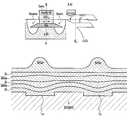
- FIG. 1 aschematically depicts a typical conventional n-Si-MOSFET, which has been produced on a p-doped Si (001) wafer, and the associated position-dependent energy band edge pattern of the conduction band between two points A and B.
- SiO 2 /Si interfaceelectrons are transported from source to drain, whereby the electron flow is controlled by the gate voltage.
- a splitting of the ⁇ -valleysoccurs in known fashion, which occurs, however, with this conventional structure only in the range of a few meV.
- FIG. 1 bdepicts an n-channel-Si-MOSFET with a strained channel region. Below the Si-channel region, there is a pseudomorphically strained Ge island. This island generates a local strain field in the Si-channel above the island. Since the intrinsic lattice constant of Ge is larger than that of Si, the Si is expanded in the growth plane above the island, a situation which is reflected in the opposing arrows. The strain reduces the symmetry of the Si crystal and cancels the 6-fold degeneracy of the ⁇ -valleys. The ⁇ (2)-valleys are lowered in the growth direction and the ⁇ (4)-valleys are raised in the growth plane. Compared to the conventional structure of FIG.
- splittingcan be increased many times over.
- the depressed ⁇ (2)-valleysare filled. Since the ⁇ (2)-valleys in the growth plane have an approximately 5-fold smaller effective mass than the ⁇ (4)-valleys, the charge carrier mobility can be drastically increased in this manner.
- the greater splittingalso results in the fact that charge carrier scattering processes are reduced.
- FIG. 7depicts a transistor structure according to the invention schematically in a top plan view.
- the Ge island structuresare arranged linearly along the gate width and connect the source and drain regions to each other.
- the gate widthis discernibly clearly longer than the gate length.
- the gate lengths used nowadays in MOS technologyare typically 100-200 nm, whereby it is to be anticipated that in the future an additional shortening will occur in accordance with Moore's Law.
- the island structuresmust be arranged in a chain or in a line along the gate width. Consequently, for mass integration, the production of parallel island chains is extremely advantageous. It should be mentioned here already that, with the process according to the invention, islands arranged in chains also form under the source, drain and gate contacts. However, this has no effect on the function of the transistor components.
- FIG. 8schematically depicts a process for the production of linear Si—Ge island structures on a Si substrate.
- linear ditches or depressions 1 a , 1 bare formed in a (001)-oriented Si substrate.
- an alternating sequence of Si layers and germanium-rich SiGe layersis then initially grown.
- the formation of a strain fieldoccurs in the region of the depressions 1 a , 1 b , which continues upward during the growth of additional layers.
- a continuing planarization of the structureis obtained.
- a SiGe layer with an adequate amount of material and germanium concentrationis grown, the formation of island structures along the lines provided by the prestructuring occurs.
- the distance between the linear structuresshould be within the range of the diffusion lengths of the atoms being added and distributed on the surface in the growth process. In the present case, the diffusion length is approximately 250 nm. It is completely possible that under optimum growth conditions, only a single Ge-rich SiGe layer suffices.
- a first SiGe layercan also be initially grown on an unstructured Si substrate and then the SiGe layer can be structured in the above-described manner.
- the coherent Ge islandstypically have a diameter of approximately 10 to several 100 nm. These dimensions thus correspond very well to the gate lengths obtainable currently and in the near future.
- source and drain regionscan then be generated by diffusion or implantation into the transistor structure on two opposite end sections of the island structures, such that in each island layer the source and drain regions are connected to each other by the islands.
- a p-channel transistor like that depicted in FIG. 1 c with an associated position-dependent energy band edge patterncan be realized with the concept according to the invention.
- the capability of production according to the invention of p-channel transistorsis of critical significance for the production according to the invention of components produced in CMOS technology (see FIG. 6 ).
- FIG. 1 ddepicts an embodiment according to this concept, wherein a plurality of island layers are arranged on top of each other in order to generate a reinforced strain field in the channel region above the uppermost island layer.
- the transistorcan selectively be designed as an n- or p-channel transistor.
- the source and drain regionsmay—as depicted—but do not necessarily have to, extend to the uppermost island layer. In the present case, it is advantageous for them to be formed as flat doping regions.
- FIG. 2 aA variant with a buried Si channel region is depicted in FIG. 2 a .
- an additional Ge island layeris grown after growth of the Si channel layer.
- the channel regionis thus embedded between two island layers, whereby a relatively large strain field is generated in the channel region.
- This structurecan also be multiplied so to speak according to FIG. 2 b , in that a plurality of island layers are generated on top of each other and several or all of the Si layers located between them are used as channel regions, in that the source and drain regions are formed as far as the depth of the lowest island layer.
- the transistors depicted in FIGS. 2 a, bmay also be designed as p-channel transistors.
- FIGS. 3 a, bdepict embodiments according to a second aspect of the present invention.
- the channel regionis formed by the island structures themselves, i.e., the source-drain current of the transistor flows through the islands.
- FIG. 3 adepicts an exemplary embodiment in which the island layer is located on the surface of the transistor
- FIG. 3 bdepicts a buried island structure whereby yet another Si layer was grown on the island layer.
- the burying of the island structurehas the advantage that an interface that has better characteristics than a Ge/SiO 2 -interface is generated between the Ge island and Si material in the upward direction as well.
- the two structures depictedmay be designed both as an n- and as a p-channel transistor.
- a position-dependent energy band edge pattern of the valence bandis depicted with respect to a p-channel transistor.
- FIGS. 4 a, bFor the Si/Ge material system and in FIG. 5 for the GaAs/InGaAs material system.
- FIGS. 4 a, bdepicts this concept with reference to a p-channel transistor wherein the channel is formed by Ge islands.
- a highly doped p + -doped Si layeris embedded above the channel region in the surrounding n-doped Si.
- this layeris arranged below the channel region.
- a highly doped n + -layeris embedded in the midst of surrounding p-doped GaAs above an island of n-doped InGaAs of a GaAs-n-channel field-effect transistor.
- Such MODFET structuresmay also be used on embodiments according to FIGS. 1 and 2, in which the channel region is formed by strained semiconductor material.
- FIG. 6depicts yet another complete CMOS structure made up of an n-channel transistor and a p-channel transistor in which the channel region of the n-channel transistor is formed by strained silicon above island structures (left part of drawing) and the channel region of the p-channel transistor is formed by Ge islands (right part of drawing).
- This structuremay also be produced with stacked island layers.
- thermal oxidationis an important process step. Customarily, temperatures>700° C. are necessary for this.
- the epitaxial cluster layermust be able to withstand these temperatures without plastic relaxation.
- initial annealing experimentsit has already been demonstrated that the Si/Ge islands may be heated to temperatures above 1000° C. without dislocations occurring. There was merely a Si—Ge material mixing, which did not, however, interfere with the production of the oxide.
- the production steps of the semiconductor cluster and of the source/drain regionsmay in principle be performed in any order and possibly even self-adjustingly after performance of the production of the gate electrode.
- the semiconductor clustersare generated by implantation of foreign atoms or foreign ions, since these offer greater positional resolution as well as the capability of generating the clusters even in relatively deep regions.
Landscapes
- Insulated Gate Type Field-Effect Transistor (AREA)
- Thin Film Transistor (AREA)
- Metal-Oxide And Bipolar Metal-Oxide Semiconductor Integrated Circuits (AREA)
Abstract
Description
This application claims priority of German patent application number 100 25 264.8, filed May 22, 2000.
The present invention concerns a field-effect transistor based on embedded cluster or island structures made of semiconductor material and a process for its production. The invention refers both to those field-effect transistors in which the strain caused by cluster structures is used in an immediately adjacent channel region and to those field-effect transistors in which the channel region itself is formed by the cluster structures.
Already, field-effect transistors are known in which the channel region is formed from strained semiconductor material. In the publication “Electronic Mobility Enhancement in Strained-Si N-Type Metal-Oxide-Semiconductor Field-Effect Transistors” by J. Welser et al., a field-effect transistor is described in which a pseudomorphically strained Si-channel region is produced by growing a Si layer on a relaxed SiGe buffer layer. The expansion strain in the Si material of the channel region results in a change in the band structure and in a cancellation of the six-fold band degeneracy, whereby higher electron and hole nobilities may be obtained.
The disadvantages of this type of strained field-effect transistors consist, however, in that the relaxed SiGe buffer layer is a few microns thick and is thus expensive and time-consuming to produce. Moreover, these layers have a high concentration of crystal defects which are an impairment to the large-area integration of transistors.
EP 0,921,575 describes a heterostructure MIS field-effect transistor with an expansion strained channel layer whereby a first Si layer, a carbon-containing Si2−YCYlayer which serves as a canal region, and an optional second Si layer are deposited in this order on a substrate. The carbon content Y and the thickness of the Si2−YCYlayer are selected such that the carbon-containing Si material has an expansion strain and this results, in the same manner as in pure expansion-strained silicon, in a splitting of the conduction and valence bands, reduced effective masses, and an increase in the mobility of charge carriers. Expansion-strained field-effect transistors of this type are, obviously, simpler to produce, since no thick SiGe buffer layers have to be grown. The disadvantage of these transistors lies, however, in that their most important region, i.e., the channel region, is no longer formed from pure silicon, but from carbon-containing silicon, whereby the component characteristics are extremely dependent upon the carbon content and the thickness of the channel layer. Thus, it is difficult to produce these field-effect transistors with reproducible component characteristics.
The object of the present invention is to report a fundamentally new material structure for a field-effect transistor, especially for its channel region, by means of which the performance characteristics of the transistor can be improved. A further object of the invention is to report a process for its production.
A field-effect transistor according to the invention, also referred to as a DOTFET, is essentially based on the use of clusterlike or islandlike semiconductor material structures in the channel region or in the vicinity of the channel region of the field-effect transistor. The clusters may be used in two fundamentally different embodiments. According to a first embodiment, they can be arranged below the actual channel region and generate a strain field in the semiconductor material of the channel region, whereby the band structure of the semiconductor material is suitably altered. The band structure may be altered with suitable material selection such that the effective masses of the charge carriers can be reduced and their mobility can be increased. In this variant, the clusterlike structures are, however, not themselves a part of the channel region of the transistor. According to a second embodiment, the channel region itself may also be formed by the clusters or islands. Mixed forms between these two embodiments are also conceivable, wherein the source/drain current flows both through the clusters and through semiconductor layers strained by the clusters.
The field-effect transistor also has source and drain regions which run vertically at least to the channel region. In the above-described first embodiment, wherein the channel region is formed by an expansion-strained semiconductor layer formed above a cluster layer, it is advantageous that relatively flat source/drain regions are formed. However, if, according to the first embodiment a plurality of the embedded expansion-strained silicon channel regions are to be generated and used, the source/drain regions should be formed to a greater depth, possibly down to the lowest semiconductor channel layer. If the channel region according to the second embodiment is to be formed by the clusters themselves, it may be necessary that the source/drain regions be formed to at least the one cluster layer or with the use of a plurality of cluster layers to a greater depth, possibly down to the lowest cluster layer. However, this is not absolutely obligatory even with the second embodiment since the channel region can be formed uniformly from the clusters of the second semiconductor material and the surrounding first semiconductor material located above it, whereby it is then adequate if the source/drain regions only extend to the semiconductor layer located above them. Above this, the embedded island structures of the second semiconductor material can form potential cavity structures within the first semiconductor material because of a lower band gap.
An essential characteristic of the field-effect transistor according to the invention consists in that at least part of the clusters run laterally between two sections which lie either, according to the first embodiment, directly under the source/drain regions, or, according to the second embodiment, inside the source/drain regions. In the first embodiment, it is, consequently, ensured that the semiconductor channel region expansion-strained by such clusters is formed between the source and drain regions. In the second embodiment, it is guaranteed that the channel region formed by the clusters themselves is formed between the source and drain regions.
In the production of field-effect transistors according to the invention, use is made of the phenomenon that with lattice-mismatched growth of a semiconductor material on a substrate of another semiconductor material with suitable selection of material, self-organized growth of island structures on the substrate occurs according to the Stranski-Krastanov mechanism. The layer, which is applied flat, breaks down spontaneously into a three-dimensional system of clusters because the elastic energy stored in the entire system is reduced thereby and an optimum compromise between different energies partially canceling each other occurs. In EP 0,437,385 A, for example, the growth of InAs growth islands on a GaAs substrate is described. Because of the lattice mismatch, a thin InAs wetting layer initially forms, above which a further growth of InAs results in the spontaneous formation of microscopic island structures. Under certain growth conditions, the exact same behavior is observed in the growth of germanium-rich SiGe on silicon substrates. For the present invention, use is made of the fact that the islands on the surface partially relax elastically. When the semiconductor material of the substrate is again grown on such growth islands, i.e., for example, silicon material on SiGe islands, a strain field is generated in this material. Since SiGe has a higher lattice constant than Si, the silicon material exhibits an expansion strain above the SiGe islands. Such an expansion-strained silicon layer can thus be generated by growth on SiGe islands, without having to produce a multi-micron-thick, relaxed, high-dislocation SiGe layer.
For a production process of field-effect transistors according to the invention, in particular in relatively high numbers and regular arrangement, it is thus advantageous if the growth of the islands proceeds not completely self-organized but, instead, is oriented by suitable specimen preparation. In a preferred method of producing a field-effect transistor, the clusters are, for example, deliberately produced spatially on prestructured substrates such that the aforementioned conditions can be fulfilled in the subsequent production of source and drain regions deliberately for a large number off transistors. In a process according to the invention, a semiconductor substrate is prepared from a first semiconductor material, or, in a layer formed from the semiconductor substrate, at least one linear depression is formed in the surface of the semiconductor substrate, whose width is less than or equal to the gate lengths of the field-effect transistor to be reduced; alternating layers of the first semiconductor material and a second semiconductor material different from the first are repeatedly grown, until the surface is substantially planarized; and, finally, a cluster layer of the second semiconductor material is grown. Already, at the time the first growth of a layer of the second semiconductor material, in the case of SiGe, there occurs, for energy reasons, a certain material accumulation of Ge in the recessed sections and thus a strain field is generated in a Si layer deposited thereon in these regions.
In this manner, by suitable substrate preparation, it is possible to cause clusters to be generated substantially along a line such that during a subsequent process step, the source and drain regions must be formed on both sides of this line.
The field-effect transistor according to the invention can be realized in various semiconductor material systems. A first implementation possibility concerns the silicon/germanium material system. A field-effect transistor made of this material system thus includes a semiconductor substrate made of silicon and a cluster layer in which a plurality of semiconductor clusters made of SiXGe1−X(0≦X<1) are arranged on the substrate and are embedded in silicon material.
In the following, the present invention is illustrated in detail with reference to the drawings wherein, among other things, a few of the exemplary embodiments are depicted schematically.
They depict:
FIGS. 1a, ba conventional structure of an n-channel-Si-MOSFET (a) and an embodiment according to the invention of the strained n-channel-Si-MOSFET with a cluster layer and, located above it, a strained Si-channel layer (b) with associated energy band edge patterns;
FIGS. 1c, da p-channel-Si-MOSFET (c) with an associated energy band edge pattern and an n/p-channel-Si-MOSFET with a plurality of island layers (d);
FIGS. 2a, ban n-channel-Si-MOSFET with two island layers and a buried channel layer (a) and a plurality of island layers and a plurality of buried channel layers (b);
FIGS. 3a, ba Si-MOSFET with an island layer forming the channel region and an associated energy band edge pattern (a) and a buried island layer (b) forming the channel region;
FIGS. 4a, bdifferent embodiments of modulation-doped p-channel-Si-MOSFETs with a Ge island layer forming the channel region;
FIG. 5 a modulation-doped n-channel-GaAs-MOSFET with an InGaAs island layer forming the channel region;
FIG. 6 a CMOS structure with an n-channel-Si-MOSFET and a p-channel-Ge-island MOSFET;
FIG. 7 a top plan view of a field-effect transistor according to the invention with a linear arrangement of island structures;
FIG. 8 a depiction of a process according to the invention for the production of the field-effect transistor according to FIG.7.
FIGS. 1 through 6 depict in each case cross-sectional representations of MOSFET structures through the gate, the source and drain regions, and an island structure connecting the source and drain region.
Although the following description often mentions Ge islands for the sake of simplicity, the expression means in general semiconductor clusters with the material composition SiXGe1−X(0≦X<1).
FIG. 1aschematically depicts a typical conventional n-Si-MOSFET, which has been produced on a p-doped Si (001) wafer, and the associated position-dependent energy band edge pattern of the conduction band between two points A and B. On the SiO2/Si interface, electrons are transported from source to drain, whereby the electron flow is controlled by the gate voltage. As a result of the confinement on the interface, a splitting of the Δ-valleys occurs in known fashion, which occurs, however, with this conventional structure only in the range of a few meV.
In contrast with this, FIG. 1bdepicts an n-channel-Si-MOSFET with a strained channel region. Below the Si-channel region, there is a pseudomorphically strained Ge island. This island generates a local strain field in the Si-channel above the island. Since the intrinsic lattice constant of Ge is larger than that of Si, the Si is expanded in the growth plane above the island, a situation which is reflected in the opposing arrows. The strain reduces the symmetry of the Si crystal and cancels the 6-fold degeneracy of the Δ-valleys. The Δ(2)-valleys are lowered in the growth direction and the Δ(4)-valleys are raised in the growth plane. Compared to the conventional structure of FIG. 1a, splitting can be increased many times over. Upon transport of current through the transistor, the depressed Δ(2)-valleys are filled. Since the Δ(2)-valleys in the growth plane have an approximately 5-fold smaller effective mass than the Δ(4)-valleys, the charge carrier mobility can be drastically increased in this manner. The greater splitting also results in the fact that charge carrier scattering processes are reduced.
FIG. 7 depicts a transistor structure according to the invention schematically in a top plan view. The Ge island structures are arranged linearly along the gate width and connect the source and drain regions to each other. The gate width is discernibly clearly longer than the gate length. The gate lengths used nowadays in MOS technology are typically 100-200 nm, whereby it is to be anticipated that in the future an additional shortening will occur in accordance with Moore's Law.
So that a parallel arrangement of field-effect transistors is possible, the island structures must be arranged in a chain or in a line along the gate width. Consequently, for mass integration, the production of parallel island chains is extremely advantageous. It should be mentioned here already that, with the process according to the invention, islands arranged in chains also form under the source, drain and gate contacts. However, this has no effect on the function of the transistor components.
When, on an unstructured semiconductor substrate of the first semiconductor material, a second semiconductor material with a clearly different lattice constant is grown, a spontaneous and spatially random formation of island structures occurs—as already mentioned. In order to guide the island growth in a specific direction, the substrate can be prestructured. FIG. 8 schematically depicts a process for the production of linear Si—Ge island structures on a Si substrate. In this process, linear ditches ordepressions depressions
A first SiGe layer can also be initially grown on an unstructured Si substrate and then the SiGe layer can be structured in the above-described manner.
The coherent Ge islands typically have a diameter of approximately 10 to several 100 nm. These dimensions thus correspond very well to the gate lengths obtainable currently and in the near future.
It is thus possible to produce one or a plurality of island layers with chainlike island structures arranged one on top of another. In a known manner, source and drain regions can then be generated by diffusion or implantation into the transistor structure on two opposite end sections of the island structures, such that in each island layer the source and drain regions are connected to each other by the islands.
Since the Si material of the channel region strained by the strain field of the Ge islands also enables greater hole mobility, a p-channel transistor like that depicted in FIG. 1cwith an associated position-dependent energy band edge pattern can be realized with the concept according to the invention. The capability of production according to the invention of p-channel transistors is of critical significance for the production according to the invention of components produced in CMOS technology (see FIG.6).
It can be seen from the above description of a process according to the invention for the production of linear island structures that it is also possible to arrange self-organized island structures perfectly on top of each other since the strain fields once generated can continue in the growth direction indefinitely on top of each other and thus, with new growth of SiGe layers, result in the formation of growth islands with the same position dependency as in the underlying layers. It is thus possible to arrange self-organizing island structures perfectly on top of each other. Through this concept, the necessary strain fields can be massively reinforced and thus the Δ-splitting can be increased significantly. FIG. 1ddepicts an embodiment according to this concept, wherein a plurality of island layers are arranged on top of each other in order to generate a reinforced strain field in the channel region above the uppermost island layer. The transistor can selectively be designed as an n- or p-channel transistor. The source and drain regions may—as depicted—but do not necessarily have to, extend to the uppermost island layer. In the present case, it is advantageous for them to be formed as flat doping regions.
It is also possible to generate one or a plurality of channel regions buried under the surface of the transistor. A variant with a buried Si channel region is depicted in FIG. 2a. Here, in contrast to the embodiment according to FIG. 1b, an additional Ge island layer is grown after growth of the Si channel layer. The channel region is thus embedded between two island layers, whereby a relatively large strain field is generated in the channel region. This structure can also be multiplied so to speak according to FIG. 2b, in that a plurality of island layers are generated on top of each other and several or all of the Si layers located between them are used as channel regions, in that the source and drain regions are formed as far as the depth of the lowest island layer. Of course, the transistors depicted in FIGS. 2a, bmay also be designed as p-channel transistors.
FIGS. 3a, bdepict embodiments according to a second aspect of the present invention. In these embodiments, the channel region is formed by the island structures themselves, i.e., the source-drain current of the transistor flows through the islands. FIG. 3adepicts an exemplary embodiment in which the island layer is located on the surface of the transistor, whereas FIG. 3bdepicts a buried island structure whereby yet another Si layer was grown on the island layer. The burying of the island structure has the advantage that an interface that has better characteristics than a Ge/SiO2-interface is generated between the Ge island and Si material in the upward direction as well. The two structures depicted may be designed both as an n- and as a p-channel transistor. In the right hand part of the drawing of FIG. 3a, a position-dependent energy band edge pattern of the valence band is depicted with respect to a p-channel transistor.
When, with certain material systems, no suitable gate oxide or other insulator is available, it is possible to use, as an additional embodiment according to the invention, a modulation-doped transistor structure known in the prior art. Such so-called MODFET structures are depicted in FIGS. 4a, bfor the Si/Ge material system and in FIG. 5 for the GaAs/InGaAs material system.
FIGS. 4a, bdepicts this concept with reference to a p-channel transistor wherein the channel is formed by Ge islands. In the embodiment according to FIG. 4a,a highly doped p+-doped Si layer is embedded above the channel region in the surrounding n-doped Si. In the inverted structure of FIG. 4b, this layer is arranged below the channel region. In FIG. 5, a highly doped n+-layer is embedded in the midst of surrounding p-doped GaAs above an island of n-doped InGaAs of a GaAs-n-channel field-effect transistor. Such MODFET structures may also be used on embodiments according to FIGS. 1 and 2, in which the channel region is formed by strained semiconductor material.
And finally, FIG. 6 depicts yet another complete CMOS structure made up of an n-channel transistor and a p-channel transistor in which the channel region of the n-channel transistor is formed by strained silicon above island structures (left part of drawing) and the channel region of the p-channel transistor is formed by Ge islands (right part of drawing). This structure may also be produced with stacked island layers.
In the production of field-effect transistors, both conventional and according to the invention, thermal oxidation is an important process step. Customarily, temperatures>700° C. are necessary for this. The epitaxial cluster layer must be able to withstand these temperatures without plastic relaxation. In initial annealing experiments, it has already been demonstrated that the Si/Ge islands may be heated to temperatures above 1000° C. without dislocations occurring. There was merely a Si—Ge material mixing, which did not, however, interfere with the production of the oxide.
Alternatively to the above-described process for production of a field-effect transistor according to the invention, it can also be produced in that first a layer structure of a conventional field-effect transistor is grown and then semiconductor clusters are generated at the appropriate places by diffusion or implantation. Such a process has, consequently, the following process steps:
Preparing a substrate made of a first semiconductor material;
Forming semiconductor clusters from a second semiconductor material by the addition of impurities, in particular by diffusion or implantation;
Forming source and drain regions in or above end sections of the semiconductor clusters;
Forming a gate electrode on the surface of:the transistor above the semiconductor clusters.
The production steps of the semiconductor cluster and of the source/drain regions may in principle be performed in any order and possibly even self-adjustingly after performance of the production of the gate electrode. Preferably, the semiconductor clusters are generated by implantation of foreign atoms or foreign ions, since these offer greater positional resolution as well as the capability of generating the clusters even in relatively deep regions.
Claims (26)
1. Field-effect transistor, with a semiconductor substrate made of a first semiconductor material, a cluster layer, in which a plurality of semiconductor clusters made of a second semiconductor material different from the first semiconductor material are arranged on the substrate and are at least partially surrounded by the first semiconductor material, wherein the crystal configuration of the semiconductor clusters is in an elastically or partially elastically relaxed state thereby causing a three-dimensional strain field in the surrounding first semiconductor material, source and drain regions which extend vertically at least to a channel region, whereby at least one part of the semiconductor cluster extends laterally between sections that lie below or within the source/drain regions, a channel region that is formed from the aforementioned part of the semiconductor cluster and/or from a layer of said first semiconductor material possibly deposited above said part of the semiconductor cluster, wherein the crystal configuration of the said layer is in a strained state caused by the three-dimensional strain field or fields of the at least partially surrounded and at least partially elastically relaxed clusters, and a gate electrode formed above the channel region.
2. Field-effect transistor according toclaim 1 , characterized in that
the first semiconductor material is silicon,
the second semiconductor material is SixGe1−x(0≦X<1).
3. Field-effect transistor according toclaim 1 , characterized in that
the first semiconductor material is GaAs,
the second semiconductor material is InGaAs.
4. Field-effect transistor according toclaim 1 , characterized in that on the cluster layer, a layer of the first semiconductor material is formed, which layer has the sections forming the channel region made of a strained first semiconductor material, which extend from the source region to the drain region and which lie above said part of the semiconductor cluster.
5. Field-effect transistor according toclaim 4 , characterized in that an additional cluster layer is formed on the layer of the first semiconductor material, in which cluster layer a large number of semiconductor clusters are arranged on the layer of the first semiconductor material and are surrounded by the first semiconductor material.
6. Field-effect transistor according toclaim 4 , characterized in that an alternating sequence of additional cluster layers and layers of the first semiconductor material formed thereon is arranged on the layer of the first semiconductor material, whereby the cluster layers are formed in each case in that a plurality of semiconductor clusters is arranged on the underlying layer of the first semiconductor material.
7. Field-effect transistor according toclaim 6 , characterized in that the source and drain regions extend vertically to the uppermost layer of the first semiconductor material.
8. Field-effect transistor according toclaim 6 , characterized in that the source and drain regions extend vertically to a deeper lying, possibly to the lowest layer of the first semiconductor material.
9. Field-effect transistor according toclaim 1 , characterized in that the channel region is formed by semiconductor clusters that extend from the source region to the drain region.
10. Field-effect transistor according toclaim 9 , characterized in that the gate electrode is formed directly above the cluster layer.
11. Field-effect transistor according toclaim 9 , characterized in that a layer of the first semiconductor material is formed on the cluster layer such that the cluster layer is formed as a buried layer.
12. Field-effect transistor according toclaim 1 , characterized in that it is designed as a MODFET structure.
13. Field-effect transistor according toclaim 1 , characterized in that
the semiconductor clusters are arranged linearly in the at least one cluster layer.
14. Field-effect transistor according toclaim 13 , characterized in that
a plurality of cluster layers are stacked one on top of another and the lines of the semiconductor clusters are arranged on top of each other.
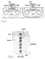
15. A CMOS semiconductor device comprising:
a p-type semiconductor substrate;
an NMOS transistor having:
NMOS transistor n-type doped source and drain zones provided in an NMOS transistor surface region of the p-type semiconductor substrate and extending to a depth from the NMOS transistor surface region,
an NMOS transistor gate electrode overlying the NMOS transistor surface region with an NMOS transistor gate dielectric layer therebetween,
an NMOS transistor n-type channel region disposed in the p-type semiconductor substrate under the NMOS transistor gate electrode and interposed between the *NMOS transistor n-type doped source and drain zones, and
an NMOS cluster layer disposed in the p-type semiconductor substrate adjacent the NMOS transistor n-type channel region and interposed between the NMOS transistor n-type doped source and drain zones, the NMOS cluster layer being configured in an elastically or partially elastically relaxed state to generate a three-dimensional strain field in the adjacent NMOS transistor n-type channel region; and
a PMOS transistor having:
PMOS transistor p-type doped source and drain zones provided in a PMOS transistor surface region of a n-type well disposed in the p-type semiconductor substrate, the PMOS transistor p-type doped source and drain zones extending to a depth from the PMOS transistor surface region,
a PMOS transistor gate electrode overlying the PMOS transistor surface region with a PMOS transistor gate dielectric layer therebetween, and
a PMOS transistor p-type channel region disposed in the n-type well under the PMOS transistor gate electrode and interposed between the PMOS transistor p-type doped source and drain zones, the PMOS transistor p-type channel region being formed by a PMOS transistor cluster layer disposed in the n-type well and interposed between the PMOS transistor p-type doped source and drain zones.
16. The CMOS transistor according toclaim 15 , wherein the p-type semiconductor substrate and the n-type well are silicon and the NMOS cluster layer and the PMOS cluster a layer are SixGe1−x(0≦X<1).
17. The CMOS transistor according toclaim 15 , wherein the p-type semiconductor substrate and the n-type well are GaAs and the NMOS cluster layer and the PMOS cluster layer are InGaAs.
18. The CMOS transistor according toclaim 15 , further comprising an alternating sequence of one or more additional NMOS n-type channel regions and one or more respective adjacent NMOS cluster layers disposed in the substrate under the NMOS transistor gate electrode and interposed between the NMOS transistor n-type doped source and drain zones.
19. An NMOS transistor comprising:
a p-type semiconductor substrate;
NMOS transistor n-type doped source and drain zones provided in an NMOS transistor surface region of the p-type semiconductor substrate and extending to a depth from the NMOS transistor surface region;
an NMOS transistor gate electrode overlying the NMOS transistor surface region with an NMOS transistor gate dielectric layer therebetween;
an NMOS transistor n-type channel region disposed in the p-type semiconductor substrate under the NMOS transistor gate electrode and interposed between the NMOS transistor n-type doped source and drain zones; and
an NMOS cluster layer disposed in the p-type semiconductor substrate adjacent the NMOS transistor n-type channel region and interposed between the NMOS transistor n-type doped source and drain zones, the NMOS cluster layer being configured in an elastically or partially elastically relaxed state to generate a three-dimensional strain field in the adjacent NMOS transistor n-type channel region.
20. The NMOS transistor according toclaim 19 , wherein the p-type semiconductor substrate is silicon and the NMOS cluster layer is SixGe1−x(0≦X<1).
21. The NMOS transistor according toclaim 19 , wherein the p-type semiconductor substrate is GaAs, and the NMOS cluster layer is InGaAs.
22. The NMOS transistor according toclaim 19 , further comprising an alternating sequence of one or more additional NMOS n-type channel regions and one or more respective adjacent NMOS cluster layers disposed in the p-type semiconductor substrate under the NMOS transistor gate electrode and interposed between the NMOS transistor n-type doped source and drain zones.
23. A PMOS transistor comprising:
an n-type semiconductor substrate;
PMOS transistor p-type doped source and drain zones provided in a PMOS transistor surface region of the n-type semiconductor substrate and extending co a depth from the PMOS transistor surface region;
a PMOS transistor gate electrode overlying the PMOS transistor surface region with a PMOS transistor gate dielectric layer therebetween;
a PMOS transistor p-type channel region disposed in the n-type semiconductor substrate under the PMOS transistor gate electrode and interposed between the PMOS transistor p-type doped source and drain zones; and
a PMOS cluster layer disposed in the n-type semiconductor substrate adjacent the PMOS transistor p-type channel region and interposed between the PMOS transistor p-type doped source and drain zones, the PMOS cluster layer being configured in an elastically or partially elastically relaxed state to generate a three-dimensional strain field in the adjacent PMOS transistor p-type channel region.
24. The PMOS transistor according toclaim 23 , wherein the n-type semiconductor substrate is silicon and the PMOS cluster layer is SixGe1−x(0<X≦1).
25. The PMOS transistor according toclaim 23 , wherein the n-type semiconductor substrate is GaAs, and the PMOS cluster layer is InGaAs.
26. The PMOS transistor according toclaim 23 , further comprising an alternating sequence of one or more additional PMOS p-type channel regions and one or more respective adjacent PMOS cluster layers disposed in the n-type semiconductor substrate under the PMOS transistor gate electrode and interposed between the PMOS transistor p-type doped source and drain zones.
Priority Applications (1)
| Application Number | Priority Date | Filing Date | Title |
|---|---|---|---|
| US10/280,172US6872625B2 (en) | 2000-05-22 | 2002-10-25 | Field-effect transistor based on embedded cluster structures and process for its production |
Applications Claiming Priority (3)
| Application Number | Priority Date | Filing Date | Title |
|---|---|---|---|
| DE10025264.8 | 2000-05-22 | ||
| DE10025264ADE10025264A1 (en) | 2000-05-22 | 2000-05-22 | Field effect transistor based on embedded cluster structures and method for its production |
| DE10025264 | 2000-05-22 |
Related Child Applications (1)
| Application Number | Title | Priority Date | Filing Date |
|---|---|---|---|
| US10/280,172DivisionUS6872625B2 (en) | 2000-05-22 | 2002-10-25 | Field-effect transistor based on embedded cluster structures and process for its production |
Publications (2)
| Publication Number | Publication Date |
|---|---|
| US20010045582A1 US20010045582A1 (en) | 2001-11-29 |
| US6498359B2true US6498359B2 (en) | 2002-12-24 |
Family
ID=7643091
Family Applications (2)
| Application Number | Title | Priority Date | Filing Date |
|---|---|---|---|
| US09/860,742Expired - Fee RelatedUS6498359B2 (en) | 2000-05-22 | 2001-05-18 | Field-effect transistor based on embedded cluster structures and process for its production |
| US10/280,172Expired - Fee RelatedUS6872625B2 (en) | 2000-05-22 | 2002-10-25 | Field-effect transistor based on embedded cluster structures and process for its production |
Family Applications After (1)
| Application Number | Title | Priority Date | Filing Date |
|---|---|---|---|
| US10/280,172Expired - Fee RelatedUS6872625B2 (en) | 2000-05-22 | 2002-10-25 | Field-effect transistor based on embedded cluster structures and process for its production |
Country Status (2)
| Country | Link |
|---|---|
| US (2) | US6498359B2 (en) |
| DE (1) | DE10025264A1 (en) |
Cited By (106)
| Publication number | Priority date | Publication date | Assignee | Title |
|---|---|---|---|---|
| US20020197803A1 (en)* | 2001-06-21 | 2002-12-26 | Amberwave Systems Corporation | Enhancement of p-type metal-oxide-semiconductor field effect transistors |
| US20030013323A1 (en)* | 2001-06-14 | 2003-01-16 | Richard Hammond | Method of selective removal of SiGe alloys |
| US20030052334A1 (en)* | 2001-06-18 | 2003-03-20 | Lee Minjoo L. | Structure and method for a high-speed semiconductor device |
| US20030057439A1 (en)* | 2001-08-09 | 2003-03-27 | Fitzgerald Eugene A. | Dual layer CMOS devices |
| US20030227013A1 (en)* | 2001-08-09 | 2003-12-11 | Amberwave Systems Corporation | Dual-channel CMOS transistors with differentially strained channels |
| US20040026765A1 (en)* | 2002-06-07 | 2004-02-12 | Amberwave Systems Corporation | Semiconductor devices having strained dual channel layers |
| US6730551B2 (en) | 2001-08-06 | 2004-05-04 | Massachusetts Institute Of Technology | Formation of planar strained layers |
| US20040206951A1 (en)* | 2003-04-18 | 2004-10-21 | Mirabedini Mohammad R. | Ion implantation in channel region of CMOS device for enhanced carrier mobility |
| US20040206950A1 (en)* | 2003-04-18 | 2004-10-21 | Agajan Suvkhanov | Ion recoil implantation and enhanced carrier mobility in CMOS device |
| US6830964B1 (en) | 2003-06-26 | 2004-12-14 | Rj Mears, Llc | Method for making semiconductor device including band-engineered superlattice |
| US6833294B1 (en) | 2003-06-26 | 2004-12-21 | Rj Mears, Llc | Method for making semiconductor device including band-engineered superlattice |
| US20040262594A1 (en)* | 2003-06-26 | 2004-12-30 | Rj Mears, Llc | Semiconductor structures having improved conductivity effective mass and methods for fabricating same |
| US20040266116A1 (en)* | 2003-06-26 | 2004-12-30 | Rj Mears, Llc | Methods of fabricating semiconductor structures having improved conductivity effective mass |
| US20050029509A1 (en)* | 2003-06-26 | 2005-02-10 | Rj Mears, Llc | Electronic device comprising active optical devices with an energy band engineered superlattice |
| US20050035470A1 (en)* | 2003-08-12 | 2005-02-17 | Chih-Hsin Ko | Strained channel complementary field-effect transistors and methods of manufacture |
| US20050035410A1 (en)* | 2003-08-15 | 2005-02-17 | Yee-Chia Yeo | Semiconductor diode with reduced leakage |
| US20050035409A1 (en)* | 2003-08-15 | 2005-02-17 | Chih-Hsin Ko | Structure and method of a strained channel transistor and a second semiconductor component in an integrated circuit |
| US20050093067A1 (en)* | 2003-04-30 | 2005-05-05 | Yee-Chia Yeo | Semiconductor-on-insulator chip incorporating strained-channel partially-depleted, fully-depleted, and multiple-gate transistors |
| US20050156274A1 (en)* | 2003-04-25 | 2005-07-21 | Yee-Chia Yeo | Strained channel transistor and methods of manufacture |
| US20050170591A1 (en)* | 2003-06-26 | 2005-08-04 | Rj Mears, Llc | Method for making a semiconductor device including a superlattice and adjacent semiconductor layer with doped regions defining a semiconductor junction |
| US20050167649A1 (en)* | 2003-06-26 | 2005-08-04 | Rj Mears, Llc | Semiconductor device including a superlattice and adjacent semiconductor layer with doped regions defining a semiconductor junction |
| US20050170590A1 (en)* | 2003-06-26 | 2005-08-04 | Rj Mears, Llc. | Method for making a semiconductor device including a superlattice with regions defining a semiconductor junction |
| US20050167653A1 (en)* | 2003-06-26 | 2005-08-04 | Rj Mears, Llc | Semiconductor device including a superlattice with regions defining a semiconductor junction |
| US6946371B2 (en) | 2002-06-10 | 2005-09-20 | Amberwave Systems Corporation | Methods of fabricating semiconductor structures having epitaxially grown source and drain elements |
| US20050205929A1 (en)* | 2004-03-16 | 2005-09-22 | Hajime Nagano | Semiconductor substrate, manufacturing method therefor, and semiconductor device |
| US20050224798A1 (en)* | 2004-04-06 | 2005-10-13 | Texas Instruments, Incorporated | Process to improve transistor drive current through the use of strain |
| US20050233552A1 (en)* | 2003-04-03 | 2005-10-20 | Chung-Hu Ke | Strained channel on insulator device |
| US20050282330A1 (en)* | 2003-06-26 | 2005-12-22 | Rj Mears, Llc | Method for making a semiconductor device including a superlattice having at least one group of substantially undoped layers |
| US20050279991A1 (en)* | 2003-06-26 | 2005-12-22 | Rj Mears, Llc | Semiconductor device including a superlattice having at least one group of substantially undoped layers |
| US6982474B2 (en)* | 2002-06-25 | 2006-01-03 | Amberwave Systems Corporation | Reacted conductive gate electrodes |
| US20060011905A1 (en)* | 2003-06-26 | 2006-01-19 | Rj Mears, Llc | Semiconductor device comprising a superlattice dielectric interface layer |
| US20060019454A1 (en)* | 2003-06-26 | 2006-01-26 | Rj Mears, Llc | Method for making a semiconductor device comprising a superlattice dielectric interface layer |
| US20060024874A1 (en)* | 2004-07-30 | 2006-02-02 | Eun-Jung Yun | Methods of forming a multi-bridge-channel MOSFET |
| US20060040503A1 (en)* | 2004-08-17 | 2006-02-23 | Sun-Jay Chang | Process for fabricating a strained channel MOSFET device |
| US20060076625A1 (en)* | 2004-09-25 | 2006-04-13 | Lee Sung-Young | Field effect transistors having a strained silicon channel and methods of fabricating same |
| US20060194387A1 (en)* | 2005-02-25 | 2006-08-31 | Chih-Hao Wang | High performance transistors with SiGe strain |
| US20060202189A1 (en)* | 2003-06-26 | 2006-09-14 | Rj Mears, Llc | Semiconductor device including a memory cell with a negative differential resistance (ndr) device |
| US20060220118A1 (en)* | 2003-06-26 | 2006-10-05 | Rj Mears, Llc | Semiconductor device including a dopant blocking superlattice |
| US20060226487A1 (en)* | 2003-08-18 | 2006-10-12 | Yee-Chia Yeo | Resistor with reduced leakage |
| US20060228872A1 (en)* | 2005-03-30 | 2006-10-12 | Bich-Yen Nguyen | Method of making a semiconductor device having an arched structure strained semiconductor layer |
| US20060226492A1 (en)* | 2005-03-30 | 2006-10-12 | Bich-Yen Nguyen | Semiconductor device featuring an arched structure strained semiconductor layer |
| US20060231857A1 (en)* | 2003-06-26 | 2006-10-19 | Rj Mears, Llc | Method for making a semiconductor device including a memory cell with a negative differential resistance (ndr) device |
| US20060243964A1 (en)* | 2003-06-26 | 2006-11-02 | Rj Mears, Llc | Method for making a semiconductor device having a semiconductor-on-insulator configuration and a superlattice |
| US20060261327A1 (en)* | 2003-06-26 | 2006-11-23 | Rj Mears, Llc | Semiconductor device having a semiconductor-on-insulator configuration and a superlattice |
| US20060267130A1 (en)* | 2003-06-26 | 2006-11-30 | Rj Mears, Llc | Semiconductor Device Including Shallow Trench Isolation (STI) Regions with a Superlattice Therebetween |
| US20060270169A1 (en)* | 2003-06-26 | 2006-11-30 | Rj Mears, Llc | Method for Making a Semiconductor Device Including Shallow Trench Isolation (STI) Regions with a Superlattice Therebetween |
| US20060273299A1 (en)* | 2003-06-26 | 2006-12-07 | Rj Mears, Llc | Method for making a semiconductor device including a dopant blocking superlattice |
| US7153763B2 (en) | 2003-06-26 | 2006-12-26 | Rj Mears, Llc | Method for making a semiconductor device including band-engineered superlattice using intermediate annealing |
| US20060292818A1 (en)* | 2003-06-26 | 2006-12-28 | Rj Mears, Llc | Method for Making a Semiconductor Device Having a Semiconductor-on-Insulator (SOI) Configuration and Including a Superlattice on a Thin Semiconductor Layer |
| US20060292765A1 (en)* | 2003-06-26 | 2006-12-28 | Rj Mears, Llc | Method for Making a FINFET Including a Superlattice |
| US20060292889A1 (en)* | 2003-06-26 | 2006-12-28 | Rj Mears, Llc | FINFET Including a Superlattice |
| US20060289049A1 (en)* | 2003-06-26 | 2006-12-28 | Rj Mears, Llc | Semiconductor Device Having a Semiconductor-on-Insulator (SOI) Configuration and Including a Superlattice on a Thin Semiconductor Layer |
| US20070007508A1 (en)* | 2003-06-26 | 2007-01-11 | Rj Mears, Llc | Semiconductor Device Including a Strained Superlattice Layer Above a Stress Layer |
| US20070010040A1 (en)* | 2003-06-26 | 2007-01-11 | Rj Mears, Llc | Method for Making a Semiconductor Device Including a Strained Superlattice Layer Above a Stress Layer |
| US20070012909A1 (en)* | 2003-06-26 | 2007-01-18 | Rj Mears, Llc | Semiconductor Device Including a Strained Superlattice Between at Least One Pair of Spaced Apart Stress Regions |
| US20070015344A1 (en)* | 2003-06-26 | 2007-01-18 | Rj Mears, Llc | Method for Making a Semiconductor Device Including a Strained Superlattice Between at Least One Pair of Spaced Apart Stress Regions |
| US20070012911A1 (en)* | 2003-06-26 | 2007-01-18 | Rj Mears, Llc | Semiconductor Device Including Regions of Band-Engineered Semiconductor Superlattice to Reduce Device-On Resistance |
| US20070012912A1 (en)* | 2003-06-26 | 2007-01-18 | Rj Mears, Llc | Semiconductor Device Including a Strained Superlattice and Overlying Stress Layer and Related Methods |
| US20070012999A1 (en)* | 2003-06-26 | 2007-01-18 | Rj Mears, Llc | Method for Making a Semiconductor Device Including Regions of Band-Engineered Semiconductor Superlattice to Reduce Device-On Resistance |
| US20070020860A1 (en)* | 2003-06-26 | 2007-01-25 | Rj Mears, Llc | Method for Making Semiconductor Device Including a Strained Superlattice and Overlying Stress Layer and Related Methods |
| US20070020833A1 (en)* | 2003-06-26 | 2007-01-25 | Rj Mears, Llc | Method for Making a Semiconductor Device Including a Channel with a Non-Semiconductor Layer Monolayer |
| US20070063185A1 (en)* | 2003-06-26 | 2007-03-22 | Rj Mears, Llc | Semiconductor device including a front side strained superlattice layer and a back side stress layer |
| US20070063186A1 (en)* | 2003-06-26 | 2007-03-22 | Rj Mears, Llc | Method for making a semiconductor device including a front side strained superlattice layer and a back side stress layer |
| US20070082470A1 (en)* | 2000-08-07 | 2007-04-12 | Amberwave System Corporation | Gate technology for strained surface channel and strained buried channel MOSFET devices |
| US20070158640A1 (en)* | 2005-12-22 | 2007-07-12 | Rj Mears, Llc | Electronic device including a poled superlattice having a net electrical dipole moment |
| US20070161138A1 (en)* | 2005-12-22 | 2007-07-12 | Rj Mears, Llc | Method for making an electronic device including a poled superlattice having a net electrical dipole moment |
| US7256142B2 (en) | 2001-03-02 | 2007-08-14 | Amberwave Systems Corporation | Relaxed SiGe platform for high speed CMOS electronics and high speed analog circuits |
| US20070194298A1 (en)* | 2006-02-21 | 2007-08-23 | Rj Mears, Llc | Semiconductor device comprising a lattice matching layer |
| US7338834B2 (en) | 2006-03-17 | 2008-03-04 | Acorn Technologies, Inc. | Strained silicon with elastic edge relaxation |
| US7354843B2 (en) | 2003-07-25 | 2008-04-08 | Taiwan Semiconductor Manufacturing Company, Ltd. | Method of forming a capacitor that includes forming a bottom electrode in a strained silicon layer |
| US20080142842A1 (en)* | 2002-08-27 | 2008-06-19 | Taiwan Semiconductor Manufacturing Company, Ltd. | Relaxed silicon germanium substrate with low defect density |
| US20080179588A1 (en)* | 2007-01-25 | 2008-07-31 | Mears Technologies, Inc. | Semiconductor device including a metal-to-semiconductor superlattice interface layer and related methods |
| US20080197340A1 (en)* | 2007-02-16 | 2008-08-21 | Rj Mears, Llc | Multiple-wavelength opto-electronic device including a superlattice |
| US20080197341A1 (en)* | 2007-02-16 | 2008-08-21 | Rj Mears, Llc | Method for making a multiple-wavelength opto-electronic device including a superlattice |
| US20080258134A1 (en)* | 2007-04-23 | 2008-10-23 | Mears Technologies, Inc. | Method for making a semiconductor device including shallow trench isolation (sti) regions with maskless superlattice deposition following sti formation and related structures |
| US7504704B2 (en) | 2003-03-07 | 2009-03-17 | Amberwave Systems Corporation | Shallow trench isolation process |
| US7586165B2 (en) | 2003-06-26 | 2009-09-08 | Mears Technologies, Inc. | Microelectromechanical systems (MEMS) device including a superlattice |
| US7615829B2 (en) | 2002-06-07 | 2009-11-10 | Amberwave Systems Corporation | Elevated source and drain elements for strained-channel heterojuntion field-effect transistors |
| US7659539B2 (en) | 2003-06-26 | 2010-02-09 | Mears Technologies, Inc. | Semiconductor device including a floating gate memory cell with a superlattice channel |
| US7700416B1 (en) | 2008-04-25 | 2010-04-20 | Acorn Technologies, Inc. | Tensile strained semiconductor on insulator using elastic edge relaxation and a sacrificial stressor layer |
| US7745279B2 (en) | 2003-07-25 | 2010-06-29 | Taiwan Semiconductor Manufacturing Company, Ltd. | Capacitor that includes high permittivity capacitor dielectric |
| US7781827B2 (en) | 2007-01-24 | 2010-08-24 | Mears Technologies, Inc. | Semiconductor device with a vertical MOSFET including a superlattice and related methods |
| US7808051B2 (en) | 2008-09-29 | 2010-10-05 | Taiwan Semiconductor Manufacturing Company, Ltd. | Standard cell without OD space effect in Y-direction |
| US20100308374A1 (en)* | 2008-02-05 | 2010-12-09 | Globalfoundries Singapore Pte. Ltd. | Strained channel transistor structure and method |
| US7851325B1 (en) | 2008-09-12 | 2010-12-14 | Acorn Technologies, Inc. | Strained semiconductor using elastic edge relaxation, a buried stressor layer and a sacrificial stressor layer |
| US7867860B2 (en)* | 2003-07-25 | 2011-01-11 | Taiwan Semiconductor Manufacturing Company, Ltd. | Strained channel transistor formation |
| US7888201B2 (en) | 2003-11-04 | 2011-02-15 | Taiwan Semiconductor Manufacturing Company, Ltd. | Semiconductor-on-insulator SRAM configured using partially-depleted and fully-depleted transistors |
| US7943961B2 (en) | 2008-03-13 | 2011-05-17 | Taiwan Semiconductor Manufacturing Company, Ltd. | Strain bars in stressed layers of MOS devices |
| US8361867B2 (en) | 2010-03-19 | 2013-01-29 | Acorn Technologies, Inc. | Biaxial strained field effect transistor devices |
| US8361868B2 (en) | 2010-04-28 | 2013-01-29 | Acorn Technologies, Inc. | Transistor with longitudinal strain in channel induced by buried stressor relaxed by implantation |
| US8386549B1 (en) | 2008-03-04 | 2013-02-26 | Acorn Technologies, Inc. | Reduced complexity adaptive multistage wiener filter |
| US8395213B2 (en) | 2010-08-27 | 2013-03-12 | Acorn Technologies, Inc. | Strained semiconductor using elastic edge relaxation of a stressor combined with buried insulating layer |
| US8558278B2 (en) | 2007-01-16 | 2013-10-15 | Taiwan Semiconductor Manufacturing Company, Ltd. | Strained transistor with optimized drive current and method of forming |
| US20140234977A1 (en)* | 2012-11-30 | 2014-08-21 | Leibniz-Institut Fuer Festkoerper-Und Werkstoffforschung Dresden E.V | Rolled-up, three-dimensional field-effect transistors and the use thereof in electronics, sensors and microfluidics |
| US8822282B2 (en) | 2001-03-02 | 2014-09-02 | Taiwan Semiconductor Manufacturing Company, Ltd. | Methods of fabricating contact regions for FET incorporating SiGe |
| US9059201B2 (en) | 2010-04-28 | 2015-06-16 | Acorn Technologies, Inc. | Transistor with longitudinal strain in channel induced by buried stressor relaxed by implantation |
| US9275996B2 (en) | 2013-11-22 | 2016-03-01 | Mears Technologies, Inc. | Vertical semiconductor devices including superlattice punch through stop layer and related methods |
| US9406798B2 (en) | 2010-08-27 | 2016-08-02 | Acorn Technologies, Inc. | Strained semiconductor using elastic edge relaxation of a stressor combined with buried insulating layer |
| US9406753B2 (en) | 2013-11-22 | 2016-08-02 | Atomera Incorporated | Semiconductor devices including superlattice depletion layer stack and related methods |
| US9558939B1 (en) | 2016-01-15 | 2017-01-31 | Atomera Incorporated | Methods for making a semiconductor device including atomic layer structures using N2O as an oxygen source |
| US9716147B2 (en) | 2014-06-09 | 2017-07-25 | Atomera Incorporated | Semiconductor devices with enhanced deterministic doping and related methods |
| US9722046B2 (en) | 2014-11-25 | 2017-08-01 | Atomera Incorporated | Semiconductor device including a superlattice and replacement metal gate structure and related methods |
| US9721790B2 (en) | 2015-06-02 | 2017-08-01 | Atomera Incorporated | Method for making enhanced semiconductor structures in single wafer processing chamber with desired uniformity control |
| US9899479B2 (en) | 2015-05-15 | 2018-02-20 | Atomera Incorporated | Semiconductor devices with superlattice layers providing halo implant peak confinement and related methods |
| US10833194B2 (en) | 2010-08-27 | 2020-11-10 | Acorn Semi, Llc | SOI wafers and devices with buried stressor |
| US11289575B2 (en)* | 2020-02-04 | 2022-03-29 | United Semiconductor (Xiamen) Co., Ltd. | Semiconductor transistor having epitaxial channel layer |
Families Citing this family (7)
| Publication number | Priority date | Publication date | Assignee | Title |
|---|---|---|---|---|
| WO2002101833A1 (en)* | 2001-06-07 | 2002-12-19 | Amberwave Systems Corporation | Multiple gate insulators with strained semiconductor heterostructures |
| WO2002103801A1 (en)* | 2001-06-18 | 2002-12-27 | Massachusetts Institute Of Technology | Structures and methods for a high-speed semiconductor device |
| EP1294016A1 (en)* | 2001-09-18 | 2003-03-19 | Paul Scherrer Institut | Formation of self-organized stacked islands for self-aligned contacts of low dimensional structures |
| KR100647457B1 (en)* | 2005-12-09 | 2006-11-23 | 한국전자통신연구원 | Semiconductor device and manufacturing method |
| US8293631B2 (en) | 2008-03-13 | 2012-10-23 | International Business Machines Corporation | Semiconductor devices having tensile and/or compressive stress and methods of manufacturing |
| FR2965975B1 (en) | 2010-10-11 | 2012-12-21 | Commissariat Energie Atomique | FIELD EFFECT TRANSISTOR ON SOIL OF SELF-ASSEMBLED SEMICONDUCTOR MATERIAL |
| WO2016043769A1 (en)* | 2014-09-19 | 2016-03-24 | Intel Corporation | Apparatus and methods to create an indium gallium arsenide active channel having indium rich surfaces |
Citations (18)
| Publication number | Priority date | Publication date | Assignee | Title |
|---|---|---|---|---|
| US4710788A (en)* | 1985-11-30 | 1987-12-01 | Licentia Patent-Verwaltungs-Gmbh | Modulation doped field effect transistor with doped Six Ge1-x -intrinsic Si layering |
| US4814838A (en)* | 1986-06-02 | 1989-03-21 | Hitachi, Ltd. | Semiconductor device and method of manufacturing the same |
| US4827320A (en)* | 1986-09-19 | 1989-05-02 | University Of Illinois | Semiconductor device with strained InGaAs layer |
| US4865659A (en)* | 1986-11-27 | 1989-09-12 | Sharp Kabushiki Kaisha | Heteroepitaxial growth of SiC on Si |
| US4994866A (en)* | 1988-01-07 | 1991-02-19 | Fujitsu Limited | Complementary semiconductor device |
| EP0437385A1 (en) | 1990-01-10 | 1991-07-17 | France Telecom | Semiconductor structure for optoelectronic devices |
| JPH03227530A (en)* | 1990-02-01 | 1991-10-08 | Nec Corp | Field effect transistor and manufacture thereof |
| US5057880A (en)* | 1989-10-23 | 1991-10-15 | Fujitsu Limited | Semiconductor device having a heteroepitaxial substrate |
| JPH05129635A (en)* | 1991-11-05 | 1993-05-25 | Hitachi Ltd | Field effect transistor and production thereof |
| US5241214A (en)* | 1991-04-29 | 1993-08-31 | Massachusetts Institute Of Technology | Oxides and nitrides of metastabale group iv alloys and nitrides of group iv elements and semiconductor devices formed thereof |
| US5245208A (en)* | 1991-04-22 | 1993-09-14 | Mitsubishi Denki Kabushiki Kaisha | Semiconductor device and manufacturing method thereof |
| US5331185A (en)* | 1991-07-17 | 1994-07-19 | Sumitomo Electric Industries, Ltd. | Field effect transistor having a GaInAs/GaAs quantum well structure |
| US5357119A (en)* | 1993-02-19 | 1994-10-18 | Board Of Regents Of The University Of California | Field effect devices having short period superlattice structures using Si and Ge |
| US5461250A (en)* | 1992-08-10 | 1995-10-24 | International Business Machines Corporation | SiGe thin film or SOI MOSFET and method for making the same |
| US5461243A (en)* | 1993-10-29 | 1995-10-24 | International Business Machines Corporation | Substrate for tensilely strained semiconductor |
| US5561302A (en)* | 1994-09-26 | 1996-10-01 | Motorola, Inc. | Enhanced mobility MOSFET device and method |
| EP0921575A2 (en) | 1997-12-03 | 1999-06-09 | Matsushita Electric Industrial Co., Ltd. | Semiconductor device comprising a heterostructure MIS field-effect transistor having a strained channel layer |
| US6424004B2 (en)* | 1997-12-16 | 2002-07-23 | Hyundai Electronics Industries Co., Ltd. | Semiconductor device having quantum dots |
Family Cites Families (2)
| Publication number | Priority date | Publication date | Assignee | Title |
|---|---|---|---|---|
| US5227644A (en)* | 1989-07-06 | 1993-07-13 | Nec Corporation | Heterojunction field effect transistor with improve carrier density and mobility |
| US6723621B1 (en)* | 1997-06-30 | 2004-04-20 | International Business Machines Corporation | Abrupt delta-like doping in Si and SiGe films by UHV-CVD |
- 2000
- 2000-05-22DEDE10025264Apatent/DE10025264A1/ennot_activeWithdrawn
- 2001
- 2001-05-18USUS09/860,742patent/US6498359B2/ennot_activeExpired - Fee Related
- 2002
- 2002-10-25USUS10/280,172patent/US6872625B2/ennot_activeExpired - Fee Related
Patent Citations (19)
| Publication number | Priority date | Publication date | Assignee | Title |
|---|---|---|---|---|
| US4710788A (en)* | 1985-11-30 | 1987-12-01 | Licentia Patent-Verwaltungs-Gmbh | Modulation doped field effect transistor with doped Six Ge1-x -intrinsic Si layering |
| US4814838A (en)* | 1986-06-02 | 1989-03-21 | Hitachi, Ltd. | Semiconductor device and method of manufacturing the same |
| US4827320A (en)* | 1986-09-19 | 1989-05-02 | University Of Illinois | Semiconductor device with strained InGaAs layer |
| US4865659A (en)* | 1986-11-27 | 1989-09-12 | Sharp Kabushiki Kaisha | Heteroepitaxial growth of SiC on Si |
| US4994866A (en)* | 1988-01-07 | 1991-02-19 | Fujitsu Limited | Complementary semiconductor device |
| US5057880A (en)* | 1989-10-23 | 1991-10-15 | Fujitsu Limited | Semiconductor device having a heteroepitaxial substrate |
| US5075742A (en)* | 1990-01-10 | 1991-12-24 | French State Represented By The Minister Of The Post, Telecommunications And Space | Semiconductor structure for optoelectronic components with inclusions |
| EP0437385A1 (en) | 1990-01-10 | 1991-07-17 | France Telecom | Semiconductor structure for optoelectronic devices |
| JPH03227530A (en)* | 1990-02-01 | 1991-10-08 | Nec Corp | Field effect transistor and manufacture thereof |
| US5245208A (en)* | 1991-04-22 | 1993-09-14 | Mitsubishi Denki Kabushiki Kaisha | Semiconductor device and manufacturing method thereof |
| US5241214A (en)* | 1991-04-29 | 1993-08-31 | Massachusetts Institute Of Technology | Oxides and nitrides of metastabale group iv alloys and nitrides of group iv elements and semiconductor devices formed thereof |
| US5331185A (en)* | 1991-07-17 | 1994-07-19 | Sumitomo Electric Industries, Ltd. | Field effect transistor having a GaInAs/GaAs quantum well structure |
| JPH05129635A (en)* | 1991-11-05 | 1993-05-25 | Hitachi Ltd | Field effect transistor and production thereof |
| US5461250A (en)* | 1992-08-10 | 1995-10-24 | International Business Machines Corporation | SiGe thin film or SOI MOSFET and method for making the same |
| US5357119A (en)* | 1993-02-19 | 1994-10-18 | Board Of Regents Of The University Of California | Field effect devices having short period superlattice structures using Si and Ge |
| US5461243A (en)* | 1993-10-29 | 1995-10-24 | International Business Machines Corporation | Substrate for tensilely strained semiconductor |
| US5561302A (en)* | 1994-09-26 | 1996-10-01 | Motorola, Inc. | Enhanced mobility MOSFET device and method |
| EP0921575A2 (en) | 1997-12-03 | 1999-06-09 | Matsushita Electric Industrial Co., Ltd. | Semiconductor device comprising a heterostructure MIS field-effect transistor having a strained channel layer |
| US6424004B2 (en)* | 1997-12-16 | 2002-07-23 | Hyundai Electronics Industries Co., Ltd. | Semiconductor device having quantum dots |
Non-Patent Citations (3)
| Title |
|---|
| J. Welser et al., "Electronic Mobility Enhancement in Strained-Si N-Type Metal-oxide-Semiconductor Field-Effect Transistors." IEEE Electron Device Letters, vol. 15, No. 3, Mar. 1994, pp 100-102. |
| Murakami et al., Ultra High Hole Mobility in Strain-Controlled Si-Ge Modulation-Doped FET, 1990, IEEE, IEDM, pp. 375-378.** |
| Wang et al., High Hole Mobility Transistor (HHMT) With Dual Si/Ge0.4Si0.6/Si Wells Structure Grown by Si MBE, IEEE, EDMS '94, pp. 2-5-17 to 2-5-20.** |
Cited By (232)
| Publication number | Priority date | Publication date | Assignee | Title |
|---|---|---|---|---|
| US20070082470A1 (en)* | 2000-08-07 | 2007-04-12 | Amberwave System Corporation | Gate technology for strained surface channel and strained buried channel MOSFET devices |
| US7256142B2 (en) | 2001-03-02 | 2007-08-14 | Amberwave Systems Corporation | Relaxed SiGe platform for high speed CMOS electronics and high speed analog circuits |
| US7501351B2 (en) | 2001-03-02 | 2009-03-10 | Amberwave Systems Corporation | Relaxed SiGe platform for high speed CMOS electronics and high speed analog circuits |
| US8822282B2 (en) | 2001-03-02 | 2014-09-02 | Taiwan Semiconductor Manufacturing Company, Ltd. | Methods of fabricating contact regions for FET incorporating SiGe |
| US20040171223A1 (en)* | 2001-06-14 | 2004-09-02 | Amberwave Systems Corporation | Method of selective removal of SiGe alloys |
| US20030013323A1 (en)* | 2001-06-14 | 2003-01-16 | Richard Hammond | Method of selective removal of SiGe alloys |
| US6900094B2 (en) | 2001-06-14 | 2005-05-31 | Amberwave Systems Corporation | Method of selective removal of SiGe alloys |
| US20080128747A1 (en)* | 2001-06-18 | 2008-06-05 | Lee Minjoo L | STRUCTURE AND METHOD FOR A HIGH-SPEED SEMICONDUCTOR DEVICE HAVING A Ge CHANNEL LAYER |
| US7301180B2 (en)* | 2001-06-18 | 2007-11-27 | Massachusetts Institute Of Technology | Structure and method for a high-speed semiconductor device having a Ge channel layer |
| US20030052334A1 (en)* | 2001-06-18 | 2003-03-20 | Lee Minjoo L. | Structure and method for a high-speed semiconductor device |
| US8436336B2 (en)* | 2001-06-18 | 2013-05-07 | Massachusetts Institute Of Technology | Structure and method for a high-speed semiconductor device having a Ge channel layer |
| US20020197803A1 (en)* | 2001-06-21 | 2002-12-26 | Amberwave Systems Corporation | Enhancement of p-type metal-oxide-semiconductor field effect transistors |
| US6916727B2 (en) | 2001-06-21 | 2005-07-12 | Massachusetts Institute Of Technology | Enhancement of P-type metal-oxide-semiconductor field effect transistors |
| US20050151164A1 (en)* | 2001-06-21 | 2005-07-14 | Amberwave Systems Corporation | Enhancement of p-type metal-oxide-semiconductor field effect transistors |
| US20040164318A1 (en)* | 2001-08-06 | 2004-08-26 | Massachusetts Institute Of Technology | Structures with planar strained layers |
| US7141820B2 (en) | 2001-08-06 | 2006-11-28 | Amberwave Systems Corporation | Structures with planar strained layers |
| US6730551B2 (en) | 2001-08-06 | 2004-05-04 | Massachusetts Institute Of Technology | Formation of planar strained layers |
| US7138649B2 (en) | 2001-08-09 | 2006-11-21 | Amberwave Systems Corporation | Dual-channel CMOS transistors with differentially strained channels |
| US7465619B2 (en) | 2001-08-09 | 2008-12-16 | Amberwave Systems Corporation | Methods of fabricating dual layer semiconductor devices |
| US20030227013A1 (en)* | 2001-08-09 | 2003-12-11 | Amberwave Systems Corporation | Dual-channel CMOS transistors with differentially strained channels |
| US20030057439A1 (en)* | 2001-08-09 | 2003-03-27 | Fitzgerald Eugene A. | Dual layer CMOS devices |
| US20050221550A1 (en)* | 2001-08-09 | 2005-10-06 | Amberwave Systems Corporation | Dual layer semiconductor devices |
| US6974735B2 (en) | 2001-08-09 | 2005-12-13 | Amberwave Systems Corporation | Dual layer Semiconductor Devices |
| US20040026765A1 (en)* | 2002-06-07 | 2004-02-12 | Amberwave Systems Corporation | Semiconductor devices having strained dual channel layers |
| US7566606B2 (en) | 2002-06-07 | 2009-07-28 | Amberwave Systems Corporation | Methods of fabricating semiconductor devices having strained dual channel layers |
| US7615829B2 (en) | 2002-06-07 | 2009-11-10 | Amberwave Systems Corporation | Elevated source and drain elements for strained-channel heterojuntion field-effect transistors |
| US7138310B2 (en) | 2002-06-07 | 2006-11-21 | Amberwave Systems Corporation | Semiconductor devices having strained dual channel layers |
| US7439164B2 (en) | 2002-06-10 | 2008-10-21 | Amberwave Systems Corporation | Methods of fabricating semiconductor structures having epitaxially grown source and drain elements |
| US6946371B2 (en) | 2002-06-10 | 2005-09-20 | Amberwave Systems Corporation | Methods of fabricating semiconductor structures having epitaxially grown source and drain elements |
| US7122449B2 (en) | 2002-06-10 | 2006-10-17 | Amberwave Systems Corporation | Methods of fabricating semiconductor structures having epitaxially grown source and drain elements |
| US8129821B2 (en) | 2002-06-25 | 2012-03-06 | Taiwan Semiconductor Manufacturing Co., Ltd. | Reacted conductive gate electrodes |
| US7217603B2 (en) | 2002-06-25 | 2007-05-15 | Amberwave Systems Corporation | Methods of forming reacted conductive gate electrodes |
| US6982474B2 (en)* | 2002-06-25 | 2006-01-03 | Amberwave Systems Corporation | Reacted conductive gate electrodes |
| US20080142842A1 (en)* | 2002-08-27 | 2008-06-19 | Taiwan Semiconductor Manufacturing Company, Ltd. | Relaxed silicon germanium substrate with low defect density |
| US8564018B2 (en)* | 2002-08-27 | 2013-10-22 | Taiwan Semiconductor Manufacturing Company, Ltd. | Relaxed silicon germanium substrate with low defect density |
| US7504704B2 (en) | 2003-03-07 | 2009-03-17 | Amberwave Systems Corporation | Shallow trench isolation process |
| US7029994B2 (en) | 2003-04-03 | 2006-04-18 | Taiwan Semiconductor Manufacturing Company, Ltd. | Strained channel on insulator device |
| US20050233552A1 (en)* | 2003-04-03 | 2005-10-20 | Chung-Hu Ke | Strained channel on insulator device |
| US6982229B2 (en)* | 2003-04-18 | 2006-01-03 | Lsi Logic Corporation | Ion recoil implantation and enhanced carrier mobility in CMOS device |
| US7129516B2 (en) | 2003-04-18 | 2006-10-31 | Lsi Logic Corporation | Ion recoil implantation and enhanced carrier mobility in CMOS device |
| US20050167654A1 (en)* | 2003-04-18 | 2005-08-04 | Lsi Logic Corporation | Ion recoil implantation and enhanced carrier mobility in CMOS device |
| US20040206950A1 (en)* | 2003-04-18 | 2004-10-21 | Agajan Suvkhanov | Ion recoil implantation and enhanced carrier mobility in CMOS device |
| US20040206951A1 (en)* | 2003-04-18 | 2004-10-21 | Mirabedini Mohammad R. | Ion implantation in channel region of CMOS device for enhanced carrier mobility |
| US7052964B2 (en) | 2003-04-25 | 2006-05-30 | Taiwan Semiconductor Manufacturing Company, Ltd. | Strained channel transistor and methods of manufacture |
| US20050156274A1 (en)* | 2003-04-25 | 2005-07-21 | Yee-Chia Yeo | Strained channel transistor and methods of manufacture |
| US20050093067A1 (en)* | 2003-04-30 | 2005-05-05 | Yee-Chia Yeo | Semiconductor-on-insulator chip incorporating strained-channel partially-depleted, fully-depleted, and multiple-gate transistors |
| US7268024B2 (en) | 2003-04-30 | 2007-09-11 | Taiwan Semiconductor Manufacturing Company, Ltd. | Semiconductor-on-insulator chip incorporating strained-channel partially-depleted, fully-depleted, and multiple-gate transistors |
| US20070063186A1 (en)* | 2003-06-26 | 2007-03-22 | Rj Mears, Llc | Method for making a semiconductor device including a front side strained superlattice layer and a back side stress layer |
| US20050029511A1 (en)* | 2003-06-26 | 2005-02-10 | Rj Mears, Llc | Integrated circuit comprising an active optical device having an energy band engineered superlattice |
| US20050167653A1 (en)* | 2003-06-26 | 2005-08-04 | Rj Mears, Llc | Semiconductor device including a superlattice with regions defining a semiconductor junction |
| US6927413B2 (en) | 2003-06-26 | 2005-08-09 | Rj Mears, Llc | Semiconductor device including band-engineered superlattice |
| US20050173696A1 (en)* | 2003-06-26 | 2005-08-11 | Rj Mears, Llc | Method for making a semiconductor device including a MOSFET having a band-engineered superlattice with a semiconductor cap layer providing a channel |
| US20050173697A1 (en)* | 2003-06-26 | 2005-08-11 | Rj Mears, Llc | Semiconductor device including a MOSFET having a band-engineered superlattice with a semiconductor cap layer providing a channel |
| US20050184286A1 (en)* | 2003-06-26 | 2005-08-25 | Rj Mears, Llc, State Of Incorporation: Delaware | Semiconductor device including mosfet having band-engineered superlattice |
| US20050167649A1 (en)* | 2003-06-26 | 2005-08-04 | Rj Mears, Llc | Semiconductor device including a superlattice and adjacent semiconductor layer with doped regions defining a semiconductor junction |
| US6830964B1 (en) | 2003-06-26 | 2004-12-14 | Rj Mears, Llc | Method for making semiconductor device including band-engineered superlattice |
| US6952018B2 (en) | 2003-06-26 | 2005-10-04 | Rj Mears, Llc | Semiconductor device including band-engineered superlattice |
| US20050170591A1 (en)* | 2003-06-26 | 2005-08-04 | Rj Mears, Llc | Method for making a semiconductor device including a superlattice and adjacent semiconductor layer with doped regions defining a semiconductor junction |
| US6833294B1 (en) | 2003-06-26 | 2004-12-21 | Rj Mears, Llc | Method for making semiconductor device including band-engineered superlattice |
| US20050110003A1 (en)* | 2003-06-26 | 2005-05-26 | Rj Mears, Llc | Semiconductor device comprising a superlattice with upper portions extending above adjacent upper portions of source and drain regions |
| US6958486B2 (en) | 2003-06-26 | 2005-10-25 | Rj Mears, Llc | Semiconductor device including band-engineered superlattice |
| US6897472B2 (en) | 2003-06-26 | 2005-05-24 | Rj Mears, Llc | Semiconductor device including MOSFET having band-engineered superlattice |
| US20050282330A1 (en)* | 2003-06-26 | 2005-12-22 | Rj Mears, Llc | Method for making a semiconductor device including a superlattice having at least one group of substantially undoped layers |
| US20050279991A1 (en)* | 2003-06-26 | 2005-12-22 | Rj Mears, Llc | Semiconductor device including a superlattice having at least one group of substantially undoped layers |
| US6891188B2 (en) | 2003-06-26 | 2005-05-10 | Rj Mears, Llc | Semiconductor device including band-engineered superlattice |
| US20050087736A1 (en)* | 2003-06-26 | 2005-04-28 | Rj Mears, Llc. | Semiconductor device including band-engineered superlattice having 3/1-5/1 germanium layer structure |
| US20060011905A1 (en)* | 2003-06-26 | 2006-01-19 | Rj Mears, Llc | Semiconductor device comprising a superlattice dielectric interface layer |
| US20060019454A1 (en)* | 2003-06-26 | 2006-01-26 | Rj Mears, Llc | Method for making a semiconductor device comprising a superlattice dielectric interface layer |
| US20040262597A1 (en)* | 2003-06-26 | 2004-12-30 | Rj Mears, Llc | Semiconductor device including mosfet having band-engineered superlattice |
| US20040266046A1 (en)* | 2003-06-26 | 2004-12-30 | Rj Mears, Llc | Method for making semiconductor device including band-engineered superlattice |
| US7018900B2 (en) | 2003-06-26 | 2006-03-28 | Rj Mears, Llc | Method for making a semiconductor device comprising a superlattice channel vertically stepped above source and drain regions |
| US7436026B2 (en) | 2003-06-26 | 2008-10-14 | Mears Technologies, Inc. | Semiconductor device comprising a superlattice channel vertically stepped above source and drain regions |
| US7435988B2 (en) | 2003-06-26 | 2008-10-14 | Mears Technologies, Inc. | Semiconductor device including a MOSFET having a band-engineered superlattice with a semiconductor cap layer providing a channel |
| US20050090048A1 (en)* | 2003-06-26 | 2005-04-28 | Rj Mears, Llc | Method for making a semiconductor device comprising a superlattice channel vertically stepped above source and drain regions |
| US7033437B2 (en) | 2003-06-26 | 2006-04-25 | Rj Mears, Llc | Method for making semiconductor device including band-engineered superlattice |
| US7034329B2 (en) | 2003-06-26 | 2006-04-25 | Rj Mears, Llc | Semiconductor device including band-engineered superlattice having 3/1-5/1 germanium layer structure |
| US7045377B2 (en) | 2003-06-26 | 2006-05-16 | Rj Mears, Llc | Method for making a semiconductor device including a superlattice and adjacent semiconductor layer with doped regions defining a semiconductor junction |
| US7045813B2 (en) | 2003-06-26 | 2006-05-16 | Rj Mears, Llc | Semiconductor device including a superlattice with regions defining a semiconductor junction |
| US20050087738A1 (en)* | 2003-06-26 | 2005-04-28 | R.J. Mears Llc | Method for making a semiconductor device including band-engineered superlattice having 3/1-5/1 germanium layer structure |
| US7659539B2 (en) | 2003-06-26 | 2010-02-09 | Mears Technologies, Inc. | Semiconductor device including a floating gate memory cell with a superlattice channel |
| US7071119B2 (en) | 2003-06-26 | 2006-07-04 | Rj Mears, Llc | Method for making a semiconductor device including band-engineered superlattice having 3/1-5/1 germanium layer structure |
| US20040262595A1 (en)* | 2003-06-26 | 2004-12-30 | Rj Mears Llc | Semiconductor device including band-engineered superlattice |
| US20040266116A1 (en)* | 2003-06-26 | 2004-12-30 | Rj Mears, Llc | Methods of fabricating semiconductor structures having improved conductivity effective mass |
| US20060202189A1 (en)* | 2003-06-26 | 2006-09-14 | Rj Mears, Llc | Semiconductor device including a memory cell with a negative differential resistance (ndr) device |
| US7109052B2 (en) | 2003-06-26 | 2006-09-19 | Rj Mears, Llc | Method for making an integrated circuit comprising a waveguide having an energy band engineered superlattice |
| US7612366B2 (en) | 2003-06-26 | 2009-11-03 | Mears Technologies, Inc. | Semiconductor device including a strained superlattice layer above a stress layer |
| US20060220118A1 (en)* | 2003-06-26 | 2006-10-05 | Rj Mears, Llc | Semiconductor device including a dopant blocking superlattice |
| US7598515B2 (en) | 2003-06-26 | 2009-10-06 | Mears Technologies, Inc. | Semiconductor device including a strained superlattice and overlying stress layer and related methods |
| US7586165B2 (en) | 2003-06-26 | 2009-09-08 | Mears Technologies, Inc. | Microelectromechanical systems (MEMS) device including a superlattice |
| US7586116B2 (en) | 2003-06-26 | 2009-09-08 | Mears Technologies, Inc. | Semiconductor device having a semiconductor-on-insulator configuration and a superlattice |
| US20050087737A1 (en)* | 2003-06-26 | 2005-04-28 | Rj Mears, Llc | Semiconductor device comprising a superlattice channel vertically stepped above source and drain regions |
| US20060231857A1 (en)* | 2003-06-26 | 2006-10-19 | Rj Mears, Llc | Method for making a semiconductor device including a memory cell with a negative differential resistance (ndr) device |
| US6878576B1 (en) | 2003-06-26 | 2005-04-12 | Rj Mears, Llc | Method for making semiconductor device including band-engineered superlattice |
| US20060243964A1 (en)* | 2003-06-26 | 2006-11-02 | Rj Mears, Llc | Method for making a semiconductor device having a semiconductor-on-insulator configuration and a superlattice |
| US20050170590A1 (en)* | 2003-06-26 | 2005-08-04 | Rj Mears, Llc. | Method for making a semiconductor device including a superlattice with regions defining a semiconductor junction |
| US20040262628A1 (en)* | 2003-06-26 | 2004-12-30 | Rj Mears, Llc | Semiconductor device including band-engineered superlattice |
| US20060261327A1 (en)* | 2003-06-26 | 2006-11-23 | Rj Mears, Llc | Semiconductor device having a semiconductor-on-insulator configuration and a superlattice |
| US7446002B2 (en) | 2003-06-26 | 2008-11-04 | Mears Technologies, Inc. | Method for making a semiconductor device comprising a superlattice dielectric interface layer |
| US20060267130A1 (en)* | 2003-06-26 | 2006-11-30 | Rj Mears, Llc | Semiconductor Device Including Shallow Trench Isolation (STI) Regions with a Superlattice Therebetween |
| US20060270169A1 (en)* | 2003-06-26 | 2006-11-30 | Rj Mears, Llc | Method for Making a Semiconductor Device Including Shallow Trench Isolation (STI) Regions with a Superlattice Therebetween |
| US20060273299A1 (en)* | 2003-06-26 | 2006-12-07 | Rj Mears, Llc | Method for making a semiconductor device including a dopant blocking superlattice |
| US7153763B2 (en) | 2003-06-26 | 2006-12-26 | Rj Mears, Llc | Method for making a semiconductor device including band-engineered superlattice using intermediate annealing |
| US20060292818A1 (en)* | 2003-06-26 | 2006-12-28 | Rj Mears, Llc | Method for Making a Semiconductor Device Having a Semiconductor-on-Insulator (SOI) Configuration and Including a Superlattice on a Thin Semiconductor Layer |
| US20060292765A1 (en)* | 2003-06-26 | 2006-12-28 | Rj Mears, Llc | Method for Making a FINFET Including a Superlattice |
| US20060292889A1 (en)* | 2003-06-26 | 2006-12-28 | Rj Mears, Llc | FINFET Including a Superlattice |
| US20060289049A1 (en)* | 2003-06-26 | 2006-12-28 | Rj Mears, Llc | Semiconductor Device Having a Semiconductor-on-Insulator (SOI) Configuration and Including a Superlattice on a Thin Semiconductor Layer |
| US20070007508A1 (en)* | 2003-06-26 | 2007-01-11 | Rj Mears, Llc | Semiconductor Device Including a Strained Superlattice Layer Above a Stress Layer |
| US20070010040A1 (en)* | 2003-06-26 | 2007-01-11 | Rj Mears, Llc | Method for Making a Semiconductor Device Including a Strained Superlattice Layer Above a Stress Layer |
| US20070012909A1 (en)* | 2003-06-26 | 2007-01-18 | Rj Mears, Llc | Semiconductor Device Including a Strained Superlattice Between at Least One Pair of Spaced Apart Stress Regions |
| US20070015344A1 (en)* | 2003-06-26 | 2007-01-18 | Rj Mears, Llc | Method for Making a Semiconductor Device Including a Strained Superlattice Between at Least One Pair of Spaced Apart Stress Regions |
| US20070012911A1 (en)* | 2003-06-26 | 2007-01-18 | Rj Mears, Llc | Semiconductor Device Including Regions of Band-Engineered Semiconductor Superlattice to Reduce Device-On Resistance |
| US20070012912A1 (en)* | 2003-06-26 | 2007-01-18 | Rj Mears, Llc | Semiconductor Device Including a Strained Superlattice and Overlying Stress Layer and Related Methods |
| US20070012999A1 (en)* | 2003-06-26 | 2007-01-18 | Rj Mears, Llc | Method for Making a Semiconductor Device Including Regions of Band-Engineered Semiconductor Superlattice to Reduce Device-On Resistance |
| US20070020860A1 (en)* | 2003-06-26 | 2007-01-25 | Rj Mears, Llc | Method for Making Semiconductor Device Including a Strained Superlattice and Overlying Stress Layer and Related Methods |
| US20070020833A1 (en)* | 2003-06-26 | 2007-01-25 | Rj Mears, Llc | Method for Making a Semiconductor Device Including a Channel with a Non-Semiconductor Layer Monolayer |
| US20070063185A1 (en)* | 2003-06-26 | 2007-03-22 | Rj Mears, Llc | Semiconductor device including a front side strained superlattice layer and a back side stress layer |
| US20050032260A1 (en)* | 2003-06-26 | 2005-02-10 | Rj Mears, Llc | Method for making an intetgrated circuit comprising a waveguide having an energy band engineered superlattice |
| US7202494B2 (en) | 2003-06-26 | 2007-04-10 | Rj Mears, Llc | FINFET including a superlattice |
| US20050032247A1 (en)* | 2003-06-26 | 2005-02-10 | Rj Mears, Llp | Method for making an integrated circuit comprising an active optical device having an energy band engineered superlattice |
| US7535041B2 (en) | 2003-06-26 | 2009-05-19 | Mears Technologies, Inc. | Method for making a semiconductor device including regions of band-engineered semiconductor superlattice to reduce device-on resistance |
| US7432524B2 (en) | 2003-06-26 | 2008-10-07 | Mears Technologies, Inc. | Integrated circuit comprising an active optical device having an energy band engineered superlattice |
| US7227174B2 (en) | 2003-06-26 | 2007-06-05 | Rj Mears, Llc | Semiconductor device including a superlattice and adjacent semiconductor layer with doped regions defining a semiconductor junction |
| US7229902B2 (en) | 2003-06-26 | 2007-06-12 | Rj Mears, Llc | Method for making a semiconductor device including a superlattice with regions defining a semiconductor junction |
| US7531850B2 (en) | 2003-06-26 | 2009-05-12 | Mears Technologies, Inc. | Semiconductor device including a memory cell with a negative differential resistance (NDR) device |
| US7531828B2 (en) | 2003-06-26 | 2009-05-12 | Mears Technologies, Inc. | Semiconductor device including a strained superlattice between at least one pair of spaced apart stress regions |
| US7531829B2 (en) | 2003-06-26 | 2009-05-12 | Mears Technologies, Inc. | Semiconductor device including regions of band-engineered semiconductor superlattice to reduce device-on resistance |
| US20050029510A1 (en)* | 2003-06-26 | 2005-02-10 | Rj Mears, Llc | Method for making electronic device comprising active optical devices with an energy band engineered superlattice |
| US7514328B2 (en) | 2003-06-26 | 2009-04-07 | Mears Technologies, Inc. | Method for making a semiconductor device including shallow trench isolation (STI) regions with a superlattice therebetween |
| US20040262594A1 (en)* | 2003-06-26 | 2004-12-30 | Rj Mears, Llc | Semiconductor structures having improved conductivity effective mass and methods for fabricating same |
| US20040262596A1 (en)* | 2003-06-26 | 2004-12-30 | Rj Mears, Llc. | Semiconductor device including band-engineered superlattice |
| US7265002B2 (en) | 2003-06-26 | 2007-09-04 | Rj Mears, Llc | Method for making a semiconductor device including a MOSFET having a band-engineered superlattice with a semiconductor cap layer providing a channel |
| US20050031247A1 (en)* | 2003-06-26 | 2005-02-10 | Rj Mears, Llc | Integrated circuit comprising a waveguide having an energy band engineered superlattice |
| US7491587B2 (en) | 2003-06-26 | 2009-02-17 | Mears Technologies, Inc. | Method for making a semiconductor device having a semiconductor-on-insulator (SOI) configuration and including a superlattice on a thin semiconductor layer |
| US7279699B2 (en) | 2003-06-26 | 2007-10-09 | Rj Mears, Llc | Integrated circuit comprising a waveguide having an energy band engineered superlattice |
| US7279701B2 (en) | 2003-06-26 | 2007-10-09 | Rj Mears, Llc | Semiconductor device comprising a superlattice with upper portions extending above adjacent upper portions of source and drain regions |
| US20040261695A1 (en)* | 2003-06-26 | 2004-12-30 | Rj Mears, Llc. | Method for making semiconductor device including band-engineered superlattice |
| US7288457B2 (en) | 2003-06-26 | 2007-10-30 | Rj Mears, Llc | Method for making semiconductor device comprising a superlattice with upper portions extending above adjacent upper portions of source and drain regions |
| US20050029509A1 (en)* | 2003-06-26 | 2005-02-10 | Rj Mears, Llc | Electronic device comprising active optical devices with an energy band engineered superlattice |
| US7303948B2 (en) | 2003-06-26 | 2007-12-04 | Mears Technologies, Inc. | Semiconductor device including MOSFET having band-engineered superlattice |
| US7446334B2 (en) | 2003-06-26 | 2008-11-04 | Mears Technologies, Inc. | Electronic device comprising active optical devices with an energy band engineered superlattice |
| US20040266045A1 (en)* | 2003-06-26 | 2004-12-30 | Rj Mears Llc. | Method for making semiconductor device including band-engineered superlattice |
| US20050017235A1 (en)* | 2003-06-26 | 2005-01-27 | R.J. Mears Llc | Semiconductor device including band-engineered superlattice |
| US7354843B2 (en) | 2003-07-25 | 2008-04-08 | Taiwan Semiconductor Manufacturing Company, Ltd. | Method of forming a capacitor that includes forming a bottom electrode in a strained silicon layer |
| US7745279B2 (en) | 2003-07-25 | 2010-06-29 | Taiwan Semiconductor Manufacturing Company, Ltd. | Capacitor that includes high permittivity capacitor dielectric |
| US7867860B2 (en)* | 2003-07-25 | 2011-01-11 | Taiwan Semiconductor Manufacturing Company, Ltd. | Strained channel transistor formation |
| US20050035470A1 (en)* | 2003-08-12 | 2005-02-17 | Chih-Hsin Ko | Strained channel complementary field-effect transistors and methods of manufacture |
| US7101742B2 (en) | 2003-08-12 | 2006-09-05 | Taiwan Semiconductor Manufacturing Company, Ltd. | Strained channel complementary field-effect transistors and methods of manufacture |
| US20050035409A1 (en)* | 2003-08-15 | 2005-02-17 | Chih-Hsin Ko | Structure and method of a strained channel transistor and a second semiconductor component in an integrated circuit |
| US7112495B2 (en) | 2003-08-15 | 2006-09-26 | Taiwan Semiconductor Manufacturing Company, Ltd. | Structure and method of a strained channel transistor and a second semiconductor component in an integrated circuit |
| US20050035410A1 (en)* | 2003-08-15 | 2005-02-17 | Yee-Chia Yeo | Semiconductor diode with reduced leakage |
| US7646068B2 (en) | 2003-08-15 | 2010-01-12 | Taiwan Semiconductor Manufacturing Company, Ltd. | Structure and method of a strained channel transistor and a second semiconductor component in an integrated circuit |
| US20060226487A1 (en)* | 2003-08-18 | 2006-10-12 | Yee-Chia Yeo | Resistor with reduced leakage |
| US7888201B2 (en) | 2003-11-04 | 2011-02-15 | Taiwan Semiconductor Manufacturing Company, Ltd. | Semiconductor-on-insulator SRAM configured using partially-depleted and fully-depleted transistors |
| US20050205929A1 (en)* | 2004-03-16 | 2005-09-22 | Hajime Nagano | Semiconductor substrate, manufacturing method therefor, and semiconductor device |
| CN1314120C (en)* | 2004-03-16 | 2007-05-02 | 株式会社东芝 | Semiconductor substrate, manufacturing method therefor, and semiconductor device |
| US7525154B2 (en)* | 2004-03-16 | 2009-04-28 | Kabushiki Kaisha Toshiba | Semiconductor substrate, manufacturing method therefor, and semiconductor device |
| US20060131584A1 (en)* | 2004-04-06 | 2006-06-22 | Buss Dennis D | Process to improve transistor drive current through the use of strain |
| US7023018B2 (en)* | 2004-04-06 | 2006-04-04 | Texas Instruments Incorporated | SiGe transistor with strained layers |
| US20050224798A1 (en)* | 2004-04-06 | 2005-10-13 | Texas Instruments, Incorporated | Process to improve transistor drive current through the use of strain |
| US7402483B2 (en) | 2004-07-30 | 2008-07-22 | Samsung Electronics Co., Ltd. | Methods of forming a multi-bridge-channel MOSFET |
| US20060024874A1 (en)* | 2004-07-30 | 2006-02-02 | Eun-Jung Yun | Methods of forming a multi-bridge-channel MOSFET |
| US7898028B2 (en) | 2004-08-17 | 2011-03-01 | Taiwan Semiconductor Manufacturing Company, Ltd. | Process for fabricating a strained channel MOSFET device |
| US20060040503A1 (en)* | 2004-08-17 | 2006-02-23 | Sun-Jay Chang | Process for fabricating a strained channel MOSFET device |
| US7279430B2 (en) | 2004-08-17 | 2007-10-09 | Taiwan Semiconductor Manufacturing Company, Ltd. | Process for fabricating a strained channel MOSFET device |
| US20060076625A1 (en)* | 2004-09-25 | 2006-04-13 | Lee Sung-Young | Field effect transistors having a strained silicon channel and methods of fabricating same |
| US7268362B2 (en)* | 2005-02-25 | 2007-09-11 | Taiwan Semiconductor Manufacturing Company, Ltd. | High performance transistors with SiGe strain |
| US20060194387A1 (en)* | 2005-02-25 | 2006-08-31 | Chih-Hao Wang | High performance transistors with SiGe strain |
| US20060226492A1 (en)* | 2005-03-30 | 2006-10-12 | Bich-Yen Nguyen | Semiconductor device featuring an arched structure strained semiconductor layer |
| US20060228872A1 (en)* | 2005-03-30 | 2006-10-12 | Bich-Yen Nguyen | Method of making a semiconductor device having an arched structure strained semiconductor layer |
| US20070166928A1 (en)* | 2005-12-22 | 2007-07-19 | Rj Mears, Llc | Method for making an electronic device including a selectively polable superlattice |
| US20070161138A1 (en)* | 2005-12-22 | 2007-07-12 | Rj Mears, Llc | Method for making an electronic device including a poled superlattice having a net electrical dipole moment |
| US20070158640A1 (en)* | 2005-12-22 | 2007-07-12 | Rj Mears, Llc | Electronic device including a poled superlattice having a net electrical dipole moment |
| US7517702B2 (en) | 2005-12-22 | 2009-04-14 | Mears Technologies, Inc. | Method for making an electronic device including a poled superlattice having a net electrical dipole moment |
| US20070187667A1 (en)* | 2005-12-22 | 2007-08-16 | Rj Mears, Llc | Electronic device including a selectively polable superlattice |
| US20070197006A1 (en)* | 2006-02-21 | 2007-08-23 | Rj Mears, Llc | Method for making a semiconductor device comprising a lattice matching layer |
| US7700447B2 (en) | 2006-02-21 | 2010-04-20 | Mears Technologies, Inc. | Method for making a semiconductor device comprising a lattice matching layer |
| US7718996B2 (en) | 2006-02-21 | 2010-05-18 | Mears Technologies, Inc. | Semiconductor device comprising a lattice matching layer |
| US20070194298A1 (en)* | 2006-02-21 | 2007-08-23 | Rj Mears, Llc | Semiconductor device comprising a lattice matching layer |
| US20100047977A1 (en)* | 2006-03-17 | 2010-02-25 | Acorn Technologies, Inc. | Strained silicon with elastic edge relaxation |
| US7612365B2 (en) | 2006-03-17 | 2009-11-03 | Acorn Technologies, Inc. | Strained silicon with elastic edge relaxation |
| US7977147B2 (en) | 2006-03-17 | 2011-07-12 | Acom Technologies, Inc. | Strained silicon with elastic edge relaxation |
| US20080213962A1 (en)* | 2006-03-17 | 2008-09-04 | Acorn Technologies, Inc. | Strained silicon with elastic edge relaxation |
| US7338834B2 (en) | 2006-03-17 | 2008-03-04 | Acorn Technologies, Inc. | Strained silicon with elastic edge relaxation |
| US8558278B2 (en) | 2007-01-16 | 2013-10-15 | Taiwan Semiconductor Manufacturing Company, Ltd. | Strained transistor with optimized drive current and method of forming |
| US7781827B2 (en) | 2007-01-24 | 2010-08-24 | Mears Technologies, Inc. | Semiconductor device with a vertical MOSFET including a superlattice and related methods |
| US7928425B2 (en) | 2007-01-25 | 2011-04-19 | Mears Technologies, Inc. | Semiconductor device including a metal-to-semiconductor superlattice interface layer and related methods |
| US20080179588A1 (en)* | 2007-01-25 | 2008-07-31 | Mears Technologies, Inc. | Semiconductor device including a metal-to-semiconductor superlattice interface layer and related methods |
| US7863066B2 (en) | 2007-02-16 | 2011-01-04 | Mears Technologies, Inc. | Method for making a multiple-wavelength opto-electronic device including a superlattice |
| US7880161B2 (en) | 2007-02-16 | 2011-02-01 | Mears Technologies, Inc. | Multiple-wavelength opto-electronic device including a superlattice |
| US20080197340A1 (en)* | 2007-02-16 | 2008-08-21 | Rj Mears, Llc | Multiple-wavelength opto-electronic device including a superlattice |
| US20080197341A1 (en)* | 2007-02-16 | 2008-08-21 | Rj Mears, Llc | Method for making a multiple-wavelength opto-electronic device including a superlattice |
| US8389974B2 (en) | 2007-02-16 | 2013-03-05 | Mears Technologies, Inc. | Multiple-wavelength opto-electronic device including a superlattice |
| US7812339B2 (en) | 2007-04-23 | 2010-10-12 | Mears Technologies, Inc. | Method for making a semiconductor device including shallow trench isolation (STI) regions with maskless superlattice deposition following STI formation and related structures |
| US20080258134A1 (en)* | 2007-04-23 | 2008-10-23 | Mears Technologies, Inc. | Method for making a semiconductor device including shallow trench isolation (sti) regions with maskless superlattice deposition following sti formation and related structures |
| US20100308374A1 (en)* | 2008-02-05 | 2010-12-09 | Globalfoundries Singapore Pte. Ltd. | Strained channel transistor structure and method |
| US8754447B2 (en)* | 2008-02-05 | 2014-06-17 | Globalfoundries Singapore Pte. Ltd. | Strained channel transistor structure and method |
| US8386549B1 (en) | 2008-03-04 | 2013-02-26 | Acorn Technologies, Inc. | Reduced complexity adaptive multistage wiener filter |
| US8389316B2 (en) | 2008-03-13 | 2013-03-05 | Taiwan Semiconductor Manufacturing Company, Ltd. | Strain bars in stressed layers of MOS devices |
| US7943961B2 (en) | 2008-03-13 | 2011-05-17 | Taiwan Semiconductor Manufacturing Company, Ltd. | Strain bars in stressed layers of MOS devices |
| US7700416B1 (en) | 2008-04-25 | 2010-04-20 | Acorn Technologies, Inc. | Tensile strained semiconductor on insulator using elastic edge relaxation and a sacrificial stressor layer |
| US8003486B2 (en) | 2008-09-12 | 2011-08-23 | Acorn Technologies, Inc. | Method of making a semiconductor device having a strained semiconductor active region using edge relaxation, a buried stressor layer and a sacrificial stressor layer |
| US20110092047A1 (en)* | 2008-09-12 | 2011-04-21 | Acorn Technologies, Inc. | Strained Semiconductor Using Elastic Edge Relaxation, a Buried Stressor Layer and a Sacrificial Stressor Layer |
| US7851325B1 (en) | 2008-09-12 | 2010-12-14 | Acorn Technologies, Inc. | Strained semiconductor using elastic edge relaxation, a buried stressor layer and a sacrificial stressor layer |
| US7808051B2 (en) | 2008-09-29 | 2010-10-05 | Taiwan Semiconductor Manufacturing Company, Ltd. | Standard cell without OD space effect in Y-direction |
| US8361867B2 (en) | 2010-03-19 | 2013-01-29 | Acorn Technologies, Inc. | Biaxial strained field effect transistor devices |
| US9059201B2 (en) | 2010-04-28 | 2015-06-16 | Acorn Technologies, Inc. | Transistor with longitudinal strain in channel induced by buried stressor relaxed by implantation |
| US8361868B2 (en) | 2010-04-28 | 2013-01-29 | Acorn Technologies, Inc. | Transistor with longitudinal strain in channel induced by buried stressor relaxed by implantation |
| US11791411B2 (en) | 2010-08-27 | 2023-10-17 | Acorn Semi, Llc | Relating to SOI wafers and devices with buried stressors |
| US8395213B2 (en) | 2010-08-27 | 2013-03-12 | Acorn Technologies, Inc. | Strained semiconductor using elastic edge relaxation of a stressor combined with buried insulating layer |
| US12402365B2 (en) | 2010-08-27 | 2025-08-26 | Acorn Semi, Llc | SOI wafers and devices with buried stressors |
| US9406798B2 (en) | 2010-08-27 | 2016-08-02 | Acorn Technologies, Inc. | Strained semiconductor using elastic edge relaxation of a stressor combined with buried insulating layer |
| US11978800B2 (en) | 2010-08-27 | 2024-05-07 | Acorn Semi, Llc | Strained semiconductor using elastic edge relaxation of a stressor combined with buried insulating layer |
| US10084091B2 (en) | 2010-08-27 | 2018-09-25 | Acorn Technologies, Inc. | Strained semiconductor using elastic edge relaxation of a stressor combined with buried insulating layer |
| US11476364B2 (en) | 2010-08-27 | 2022-10-18 | Acorn Semi, Llc | Strained semiconductor using elastic edge relaxation of a stressor combined with buried insulating layer |
| US11322615B2 (en) | 2010-08-27 | 2022-05-03 | Acorn Semi, Llc | SOI wafers and devices with buried stressor |
| US10950727B2 (en) | 2010-08-27 | 2021-03-16 | Acorn Semi, Llc | Strained semiconductor using elastic edge relaxation of a stressor combined with buried insulating layer |
| US10833194B2 (en) | 2010-08-27 | 2020-11-10 | Acorn Semi, Llc | SOI wafers and devices with buried stressor |
| US10580896B2 (en) | 2010-08-27 | 2020-03-03 | Acorn Semi, Llc | Strained semiconductor using elastic edge relaxation of a stressor combined with buried insulating layer |
| US20140234977A1 (en)* | 2012-11-30 | 2014-08-21 | Leibniz-Institut Fuer Festkoerper-Und Werkstoffforschung Dresden E.V | Rolled-up, three-dimensional field-effect transistors and the use thereof in electronics, sensors and microfluidics |
| US9972685B2 (en) | 2013-11-22 | 2018-05-15 | Atomera Incorporated | Vertical semiconductor devices including superlattice punch through stop layer and related methods |
| US9406753B2 (en) | 2013-11-22 | 2016-08-02 | Atomera Incorporated | Semiconductor devices including superlattice depletion layer stack and related methods |
| US9275996B2 (en) | 2013-11-22 | 2016-03-01 | Mears Technologies, Inc. | Vertical semiconductor devices including superlattice punch through stop layer and related methods |
| US10170560B2 (en) | 2014-06-09 | 2019-01-01 | Atomera Incorporated | Semiconductor devices with enhanced deterministic doping and related methods |
| US9716147B2 (en) | 2014-06-09 | 2017-07-25 | Atomera Incorporated | Semiconductor devices with enhanced deterministic doping and related methods |
| US10084045B2 (en) | 2014-11-25 | 2018-09-25 | Atomera Incorporated | Semiconductor device including a superlattice and replacement metal gate structure and related methods |
| US9722046B2 (en) | 2014-11-25 | 2017-08-01 | Atomera Incorporated | Semiconductor device including a superlattice and replacement metal gate structure and related methods |
| US9941359B2 (en) | 2015-05-15 | 2018-04-10 | Atomera Incorporated | Semiconductor devices with superlattice and punch-through stop (PTS) layers at different depths and related methods |
| US9899479B2 (en) | 2015-05-15 | 2018-02-20 | Atomera Incorporated | Semiconductor devices with superlattice layers providing halo implant peak confinement and related methods |
| US9721790B2 (en) | 2015-06-02 | 2017-08-01 | Atomera Incorporated | Method for making enhanced semiconductor structures in single wafer processing chamber with desired uniformity control |
| US9558939B1 (en) | 2016-01-15 | 2017-01-31 | Atomera Incorporated | Methods for making a semiconductor device including atomic layer structures using N2O as an oxygen source |
| US11289575B2 (en)* | 2020-02-04 | 2022-03-29 | United Semiconductor (Xiamen) Co., Ltd. | Semiconductor transistor having epitaxial channel layer |
| US11637183B2 (en) | 2020-02-04 | 2023-04-25 | United Semiconductor (Xiamen) Co., Ltd. | Method of forming a semiconductor transistor having an epitaxial channel layer |
Also Published As
| Publication number | Publication date |
|---|---|
| US6872625B2 (en) | 2005-03-29 |
| US20030042565A1 (en) | 2003-03-06 |
| US20010045582A1 (en) | 2001-11-29 |
| DE10025264A1 (en) | 2001-11-29 |
Similar Documents
| Publication | Publication Date | Title |
|---|---|---|
| US6498359B2 (en) | Field-effect transistor based on embedded cluster structures and process for its production | |
| US7023018B2 (en) | SiGe transistor with strained layers | |
| US7781799B2 (en) | Source/drain strained layers | |
| US8441000B2 (en) | Heterojunction tunneling field effect transistors, and methods for fabricating the same | |
| US7101742B2 (en) | Strained channel complementary field-effect transistors and methods of manufacture | |
| JP4301506B2 (en) | Low leakage heterojunction vertical transistor and its high performance device | |
| US6844227B2 (en) | Semiconductor devices and method for manufacturing the same | |
| US6936869B2 (en) | Heterojunction field effect transistors using silicon-germanium and silicon-carbon alloys | |
| US7057216B2 (en) | High mobility heterojunction complementary field effect transistors and methods thereof | |
| US20060237746A1 (en) | GeSOI transistor with low junction current and low junction capacitance and method for making the same | |
| US20090065808A1 (en) | Semiconductor transistor having a stressed channel | |
| US20050285212A1 (en) | Transistors with increased mobility in the channel zone and method of fabrication | |
| JP2004531901A (en) | MOSFET with strained semiconductor layer | |
| US20080116487A1 (en) | Methods of fabricating transistors having high carrier mobility and transistors fabricated thereby | |
| KR101258864B1 (en) | Strained silicon, gate engineered Fermi-FETs | |
| US6867428B1 (en) | Strained silicon NMOS having silicon source/drain extensions and method for its fabrication | |
| US20060172511A1 (en) | In situ formed halo region in a transistor device | |
| US20090206407A1 (en) | Semiconductor devices having tensile and/or compressive stress and methods of manufacturing | |
| Quinones et al. | Enhanced mobility PMOSFETs using tensile-strained Si/sub 1-y/C y layers | |
| WO2006083546A2 (en) | In situ formed halo region in a transistor device | |
| CN110729355B (en) | A Longitudinal Tunneling Field Effect Transistor with Improved Subthreshold Swing | |
| KR20030069407A (en) | Method of manufacturing a heterojunction CMOS transistor in a semiconductor device | |
| US20110079769A1 (en) | Nanometric MOS Transistor With Maximized Ration Between On-State Current and Off-State Current | |
| KR20070070868A (en) | Semiconductor device and manufacturing method thereof |
Legal Events
| Date | Code | Title | Description |
|---|---|---|---|
| AS | Assignment | Owner name:MAX-PLANCK-GESELLSCHAFT ZUR FOERDERUNG DER WISSENS Free format text:ASSIGNMENT OF ASSIGNORS INTEREST;ASSIGNORS:SCHMIDT, OLIVER G.;EBERL, KARL;REEL/FRAME:011841/0680 Effective date:20010418 | |
| FEPP | Fee payment procedure | Free format text:PAT HOLDER CLAIMS SMALL ENTITY STATUS, ENTITY STATUS SET TO SMALL (ORIGINAL EVENT CODE: LTOS); ENTITY STATUS OF PATENT OWNER: SMALL ENTITY | |
| REFU | Refund | Free format text:REFUND - PAYMENT OF MAINTENANCE FEE, 4TH YEAR, LARGE ENTITY (ORIGINAL EVENT CODE: R1551); ENTITY STATUS OF PATENT OWNER: SMALL ENTITY | |
| FPAY | Fee payment | Year of fee payment:4 | |
| SULP | Surcharge for late payment | ||
| FPAY | Fee payment | Year of fee payment:8 | |
| REMI | Maintenance fee reminder mailed | ||
| LAPS | Lapse for failure to pay maintenance fees | ||
| STCH | Information on status: patent discontinuation | Free format text:PATENT EXPIRED DUE TO NONPAYMENT OF MAINTENANCE FEES UNDER 37 CFR 1.362 | |
| FP | Lapsed due to failure to pay maintenance fee | Effective date:20141224 |