US6498091B1 - Method of using a barrier sputter reactor to remove an underlying barrier layer - Google Patents
Method of using a barrier sputter reactor to remove an underlying barrier layerDownload PDFInfo
- Publication number
- US6498091B1 US6498091B1US09/704,161US70416100AUS6498091B1US 6498091 B1US6498091 B1US 6498091B1US 70416100 AUS70416100 AUS 70416100AUS 6498091 B1US6498091 B1US 6498091B1
- Authority
- US
- United States
- Prior art keywords
- barrier layer
- hole
- barrier
- sidewalls
- layer
- Prior art date
- Legal status (The legal status is an assumption and is not a legal conclusion. Google has not performed a legal analysis and makes no representation as to the accuracy of the status listed.)
- Expired - Lifetime
Links
- 230000004888barrier functionEffects0.000titleclaimsabstractdescription157
- 238000000034methodMethods0.000titleclaimsabstractdescription72
- 238000005229chemical vapour depositionMethods0.000claimsabstractdescription38
- 238000004544sputter depositionMethods0.000claimsabstractdescription28
- 230000008569processEffects0.000claimsdescription65
- RYGMFSIKBFXOCR-UHFFFAOYSA-NCopperChemical compound[Cu]RYGMFSIKBFXOCR-UHFFFAOYSA-N0.000claimsdescription45
- 239000010949copperSubstances0.000claimsdescription45
- 229910052802copperInorganic materials0.000claimsdescription45
- 238000000151depositionMethods0.000claimsdescription32
- 229910052751metalInorganic materials0.000claimsdescription30
- 239000002184metalSubstances0.000claimsdescription30
- XKRFYHLGVUSROY-UHFFFAOYSA-NArgonChemical compound[Ar]XKRFYHLGVUSROY-UHFFFAOYSA-N0.000claimsdescription16
- 229910052715tantalumInorganic materials0.000claimsdescription13
- GUVRBAGPIYLISA-UHFFFAOYSA-Ntantalum atomChemical compound[Ta]GUVRBAGPIYLISA-UHFFFAOYSA-N0.000claimsdescription13
- 239000000758substrateSubstances0.000claimsdescription12
- 229910021645metal ionInorganic materials0.000claimsdescription11
- NJPPVKZQTLUDBO-UHFFFAOYSA-NnovaluronChemical compoundC1=C(Cl)C(OC(F)(F)C(OC(F)(F)F)F)=CC=C1NC(=O)NC(=O)C1=C(F)C=CC=C1FNJPPVKZQTLUDBO-UHFFFAOYSA-N0.000claimsdescription11
- 229910052786argonInorganic materials0.000claimsdescription10
- IJGRMHOSHXDMSA-UHFFFAOYSA-NAtomic nitrogenChemical compoundN#NIJGRMHOSHXDMSA-UHFFFAOYSA-N0.000claimsdescription8
- 238000009792diffusion processMethods0.000claimsdescription7
- 150000004767nitridesChemical class0.000claimsdescription7
- 230000001939inductive effectEffects0.000claimsdescription6
- 230000000694effectsEffects0.000claimsdescription5
- 230000008878couplingEffects0.000claimsdescription4
- 238000010168coupling processMethods0.000claimsdescription4
- 238000005859coupling reactionMethods0.000claimsdescription4
- 229910052757nitrogenInorganic materials0.000claimsdescription4
- 238000005546reactive sputteringMethods0.000claimsdescription4
- MZLGASXMSKOWSE-UHFFFAOYSA-Ntantalum nitrideChemical compound[Ta]#NMZLGASXMSKOWSE-UHFFFAOYSA-N0.000claimsdescription4
- 239000010936titaniumSubstances0.000claimsdescription3
- 229910052719titaniumInorganic materials0.000claimsdescription3
- RTAQQCXQSZGOHL-UHFFFAOYSA-NTitaniumChemical compound[Ti]RTAQQCXQSZGOHL-UHFFFAOYSA-N0.000claimsdescription2
- 150000002500ionsChemical class0.000abstractdescription11
- 230000007935neutral effectEffects0.000abstractdescription8
- 229910008482TiSiNInorganic materials0.000abstract1
- QRXWMOHMRWLFEY-UHFFFAOYSA-NisoniazideChemical compoundNNC(=O)C1=CC=NC=C1QRXWMOHMRWLFEY-UHFFFAOYSA-N0.000abstract1
- 238000005240physical vapour depositionMethods0.000description49
- 235000012431wafersNutrition0.000description25
- 238000001465metallisationMethods0.000description23
- 230000008021depositionEffects0.000description18
- 239000000463materialSubstances0.000description10
- 238000005530etchingMethods0.000description6
- 239000000126substanceSubstances0.000description6
- 238000005498polishingMethods0.000description5
- 229910001460tantalum ionInorganic materials0.000description5
- ATJFFYVFTNAWJD-UHFFFAOYSA-NTinChemical compound[Sn]ATJFFYVFTNAWJD-UHFFFAOYSA-N0.000description4
- -1argon ionsChemical class0.000description4
- 230000015572biosynthetic processEffects0.000description4
- 230000001965increasing effectEffects0.000description4
- 238000007747platingMethods0.000description4
- XUIMIQQOPSSXEZ-UHFFFAOYSA-NSiliconChemical compound[Si]XUIMIQQOPSSXEZ-UHFFFAOYSA-N0.000description3
- 229910052782aluminiumInorganic materials0.000description3
- XAGFODPZIPBFFR-UHFFFAOYSA-NaluminiumChemical compound[Al]XAGFODPZIPBFFR-UHFFFAOYSA-N0.000description3
- 239000007789gasSubstances0.000description3
- 239000003870refractory metalSubstances0.000description3
- 229910052710siliconInorganic materials0.000description3
- 239000010703siliconSubstances0.000description3
- VYPSYNLAJGMNEJ-UHFFFAOYSA-NSilicium dioxideChemical compoundO=[Si]=OVYPSYNLAJGMNEJ-UHFFFAOYSA-N0.000description2
- 238000000231atomic layer depositionMethods0.000description2
- WYEMLYFITZORAB-UHFFFAOYSA-NboscalidChemical compoundC1=CC(Cl)=CC=C1C1=CC=CC=C1NC(=O)C1=CC=CN=C1ClWYEMLYFITZORAB-UHFFFAOYSA-N0.000description2
- 238000004140cleaningMethods0.000description2
- 238000010586diagramMethods0.000description2
- 230000009977dual effectEffects0.000description2
- 238000009713electroplatingMethods0.000description2
- 238000004519manufacturing processMethods0.000description2
- 238000005268plasma chemical vapour depositionMethods0.000description2
- 238000002294plasma sputter depositionMethods0.000description2
- 239000004065semiconductorSubstances0.000description2
- 238000005477sputtering targetMethods0.000description2
- 238000002230thermal chemical vapour depositionMethods0.000description2
- 229910052581Si3N4Inorganic materials0.000description1
- BLRPTPMANUNPDV-UHFFFAOYSA-NSilaneChemical compound[SiH4]BLRPTPMANUNPDV-UHFFFAOYSA-N0.000description1
- NRTOMJZYCJJWKI-UHFFFAOYSA-NTitanium nitrideChemical group[Ti]#NNRTOMJZYCJJWKI-UHFFFAOYSA-N0.000description1
- UGACIEPFGXRWCH-UHFFFAOYSA-N[Si].[Ti]Chemical group[Si].[Ti]UGACIEPFGXRWCH-UHFFFAOYSA-N0.000description1
- 238000000637aluminium metallisationMethods0.000description1
- QVGXLLKOCUKJST-UHFFFAOYSA-Natomic oxygenChemical compound[O]QVGXLLKOCUKJST-UHFFFAOYSA-N0.000description1
- 230000008901benefitEffects0.000description1
- 239000003990capacitorSubstances0.000description1
- 239000011248coating agentSubstances0.000description1
- 238000000576coating methodMethods0.000description1
- 239000000356contaminantSubstances0.000description1
- 230000003247decreasing effectEffects0.000description1
- 238000005137deposition processMethods0.000description1
- 239000003989dielectric materialSubstances0.000description1
- 238000005429filling processMethods0.000description1
- 230000004907fluxEffects0.000description1
- 238000009616inductively coupled plasmaMethods0.000description1
- 238000001459lithographyMethods0.000description1
- VIKNJXKGJWUCNN-XGXHKTLJSA-NnorethisteroneChemical compoundO=C1CC[C@@H]2[C@H]3CC[C@](C)([C@](CC4)(O)C#C)[C@@H]4[C@@H]3CCC2=C1VIKNJXKGJWUCNN-XGXHKTLJSA-N0.000description1
- 230000003647oxidationEffects0.000description1
- 238000007254oxidation reactionMethods0.000description1
- 239000001301oxygenSubstances0.000description1
- 229910052760oxygenInorganic materials0.000description1
- 230000000149penetrating effectEffects0.000description1
- 238000001020plasma etchingMethods0.000description1
- 238000009832plasma treatmentMethods0.000description1
- 239000002243precursorSubstances0.000description1
- 229910000077silaneInorganic materials0.000description1
- 235000012239silicon dioxideNutrition0.000description1
- 239000000377silicon dioxideSubstances0.000description1
- 230000002269spontaneous effectEffects0.000description1
- 238000000992sputter etchingMethods0.000description1
- 230000003068static effectEffects0.000description1
- 238000006467substitution reactionMethods0.000description1
- 230000007704transitionEffects0.000description1
- WFKWXMTUELFFGS-UHFFFAOYSA-NtungstenChemical compound[W]WFKWXMTUELFFGS-UHFFFAOYSA-N0.000description1
- 229910052721tungstenInorganic materials0.000description1
- 239000010937tungstenSubstances0.000description1
Images


Classifications
- H—ELECTRICITY
- H01—ELECTRIC ELEMENTS
- H01L—SEMICONDUCTOR DEVICES NOT COVERED BY CLASS H10
- H01L21/00—Processes or apparatus adapted for the manufacture or treatment of semiconductor or solid state devices or of parts thereof
- H01L21/70—Manufacture or treatment of devices consisting of a plurality of solid state components formed in or on a common substrate or of parts thereof; Manufacture of integrated circuit devices or of parts thereof
- H01L21/71—Manufacture of specific parts of devices defined in group H01L21/70
- H01L21/768—Applying interconnections to be used for carrying current between separate components within a device comprising conductors and dielectrics
- H01L21/76838—Applying interconnections to be used for carrying current between separate components within a device comprising conductors and dielectrics characterised by the formation and the after-treatment of the conductors
- H01L21/76841—Barrier, adhesion or liner layers
- H01L21/76843—Barrier, adhesion or liner layers formed in openings in a dielectric
- H01L21/76844—Bottomless liners
- H—ELECTRICITY
- H01—ELECTRIC ELEMENTS
- H01L—SEMICONDUCTOR DEVICES NOT COVERED BY CLASS H10
- H01L21/00—Processes or apparatus adapted for the manufacture or treatment of semiconductor or solid state devices or of parts thereof
- H01L21/02—Manufacture or treatment of semiconductor devices or of parts thereof
- H01L21/04—Manufacture or treatment of semiconductor devices or of parts thereof the devices having potential barriers, e.g. a PN junction, depletion layer or carrier concentration layer
- H01L21/18—Manufacture or treatment of semiconductor devices or of parts thereof the devices having potential barriers, e.g. a PN junction, depletion layer or carrier concentration layer the devices having semiconductor bodies comprising elements of Group IV of the Periodic Table or AIIIBV compounds with or without impurities, e.g. doping materials
- H01L21/28—Manufacture of electrodes on semiconductor bodies using processes or apparatus not provided for in groups H01L21/20 - H01L21/268
- H01L21/283—Deposition of conductive or insulating materials for electrodes conducting electric current
- H01L21/285—Deposition of conductive or insulating materials for electrodes conducting electric current from a gas or vapour, e.g. condensation
- H01L21/28506—Deposition of conductive or insulating materials for electrodes conducting electric current from a gas or vapour, e.g. condensation of conductive layers
- H01L21/28512—Deposition of conductive or insulating materials for electrodes conducting electric current from a gas or vapour, e.g. condensation of conductive layers on semiconductor bodies comprising elements of Group IV of the Periodic Table
- H01L21/2855—Deposition of conductive or insulating materials for electrodes conducting electric current from a gas or vapour, e.g. condensation of conductive layers on semiconductor bodies comprising elements of Group IV of the Periodic Table by physical means, e.g. sputtering, evaporation
- H—ELECTRICITY
- H01—ELECTRIC ELEMENTS
- H01L—SEMICONDUCTOR DEVICES NOT COVERED BY CLASS H10
- H01L21/00—Processes or apparatus adapted for the manufacture or treatment of semiconductor or solid state devices or of parts thereof
- H01L21/02—Manufacture or treatment of semiconductor devices or of parts thereof
- H01L21/04—Manufacture or treatment of semiconductor devices or of parts thereof the devices having potential barriers, e.g. a PN junction, depletion layer or carrier concentration layer
- H01L21/18—Manufacture or treatment of semiconductor devices or of parts thereof the devices having potential barriers, e.g. a PN junction, depletion layer or carrier concentration layer the devices having semiconductor bodies comprising elements of Group IV of the Periodic Table or AIIIBV compounds with or without impurities, e.g. doping materials
- H01L21/28—Manufacture of electrodes on semiconductor bodies using processes or apparatus not provided for in groups H01L21/20 - H01L21/268
- H01L21/283—Deposition of conductive or insulating materials for electrodes conducting electric current
- H01L21/285—Deposition of conductive or insulating materials for electrodes conducting electric current from a gas or vapour, e.g. condensation
- H01L21/28506—Deposition of conductive or insulating materials for electrodes conducting electric current from a gas or vapour, e.g. condensation of conductive layers
- H01L21/28512—Deposition of conductive or insulating materials for electrodes conducting electric current from a gas or vapour, e.g. condensation of conductive layers on semiconductor bodies comprising elements of Group IV of the Periodic Table
- H01L21/28556—Deposition of conductive or insulating materials for electrodes conducting electric current from a gas or vapour, e.g. condensation of conductive layers on semiconductor bodies comprising elements of Group IV of the Periodic Table by chemical means, e.g. CVD, LPCVD, PECVD, laser CVD
- H—ELECTRICITY
- H01—ELECTRIC ELEMENTS
- H01L—SEMICONDUCTOR DEVICES NOT COVERED BY CLASS H10
- H01L21/00—Processes or apparatus adapted for the manufacture or treatment of semiconductor or solid state devices or of parts thereof
- H01L21/70—Manufacture or treatment of devices consisting of a plurality of solid state components formed in or on a common substrate or of parts thereof; Manufacture of integrated circuit devices or of parts thereof
- H01L21/71—Manufacture of specific parts of devices defined in group H01L21/70
- H01L21/768—Applying interconnections to be used for carrying current between separate components within a device comprising conductors and dielectrics
- H01L21/76838—Applying interconnections to be used for carrying current between separate components within a device comprising conductors and dielectrics characterised by the formation and the after-treatment of the conductors
- H01L21/76841—Barrier, adhesion or liner layers
- H01L21/76843—Barrier, adhesion or liner layers formed in openings in a dielectric
- H01L21/76846—Layer combinations
- H—ELECTRICITY
- H01—ELECTRIC ELEMENTS
- H01L—SEMICONDUCTOR DEVICES NOT COVERED BY CLASS H10
- H01L21/00—Processes or apparatus adapted for the manufacture or treatment of semiconductor or solid state devices or of parts thereof
- H01L21/70—Manufacture or treatment of devices consisting of a plurality of solid state components formed in or on a common substrate or of parts thereof; Manufacture of integrated circuit devices or of parts thereof
- H01L21/71—Manufacture of specific parts of devices defined in group H01L21/70
- H01L21/768—Applying interconnections to be used for carrying current between separate components within a device comprising conductors and dielectrics
- H01L21/76838—Applying interconnections to be used for carrying current between separate components within a device comprising conductors and dielectrics characterised by the formation and the after-treatment of the conductors
- H01L21/76841—Barrier, adhesion or liner layers
- H01L21/76853—Barrier, adhesion or liner layers characterized by particular after-treatment steps
- H01L21/76855—After-treatment introducing at least one additional element into the layer
- H01L21/76856—After-treatment introducing at least one additional element into the layer by treatment in plasmas or gaseous environments, e.g. nitriding a refractory metal liner
- H—ELECTRICITY
- H01—ELECTRIC ELEMENTS
- H01L—SEMICONDUCTOR DEVICES NOT COVERED BY CLASS H10
- H01L21/00—Processes or apparatus adapted for the manufacture or treatment of semiconductor or solid state devices or of parts thereof
- H01L21/70—Manufacture or treatment of devices consisting of a plurality of solid state components formed in or on a common substrate or of parts thereof; Manufacture of integrated circuit devices or of parts thereof
- H01L21/71—Manufacture of specific parts of devices defined in group H01L21/70
- H01L21/768—Applying interconnections to be used for carrying current between separate components within a device comprising conductors and dielectrics
- H01L21/76838—Applying interconnections to be used for carrying current between separate components within a device comprising conductors and dielectrics characterised by the formation and the after-treatment of the conductors
- H01L21/76841—Barrier, adhesion or liner layers
- H01L21/76853—Barrier, adhesion or liner layers characterized by particular after-treatment steps
- H01L21/76865—Selective removal of parts of the layer
Definitions
- the inventionrelates generally to processes for formation of vertical interconnects in integrated circuits.
- the inventionrelates to the use of a plasma sputter reactor for both etching and deposition.
- Modem integrated circuitsinclude several levels of metallization formed over the active semiconductor circuitry formed in the substrate, most commonly a silicon wafer.
- the multiple metallization layersare required to interconnect the millions to tens of millions of discrete semiconductor devices formed in a single integrated circuit.
- Each metallization layerincludes a dielectric layer, for example, of silicon dioxide or possibly a low-k dielectric material deposited over the previous layer, a via (or contact) hole etched through the dielectric layer, and a metallization including a vertical metallic plug filled into the hole and a horizontal interconnect formed on top of the dielectric layer.
- a dielectric layerfor example, of silicon dioxide or possibly a low-k dielectric material deposited over the previous layer, a via (or contact) hole etched through the dielectric layer, and a metallization including a vertical metallic plug filled into the hole and a horizontal interconnect formed on top of the dielectric layer.
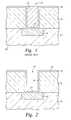
- a generic viais illustrated in the cross-sectional view of FIG. 1 . It includes a lower dielectric layer 12 (which in the case of a contact is a silicon-containing layer) having formed therein a conductive feature 14 , such as another metallization or, in the case of a contact, a contact region of a transistor.
- An upper level dielectric layer 16overlies the lower dielectric layer 12 and the conductive feature 14 .
- Advanced plasma etching processesetch a via hole 18 through the upper dielectric layer 16 to the vicinity of the conductive feature 14 .
- the holePrior to filling metallization into the via hole 18 , the hole is lined with a barrier layer 20 to prevent the diffusion of aluminum or copper into the dielectric 16 , which would short out the dielectric between neighboring via, or the diffusion of oxygen from the dielectric 16 into the metallization, which reduces the conductivity of the plug. Only thereafter is a metallization plug 22 filled into the via hole 18 .
- the filling processtypically includes a physical vapor deposition or sputtering (PVD) deposition of a copper seed layer followed by an electrochemical plating (ECP) of copper into the hole.
- PVDphysical vapor deposition or sputtering
- ECPelectrochemical plating
- the barrier structurehas become increasingly important as the lateral critical dimension has shrunk to 0.25 ⁇ m and below while the vertical dimension has remained virtually static at between 0.7 and 1.5 ⁇ m.
- the aspect ratio of the via hole 18has increased, and the electrical resistance of the vertical electrical metallization has become increasingly important.
- This emphasis on reduced vertical impedancehas been further heightened by the substitution of copper for aluminum as the most desired metallization since copper has a lower bulk resistivity.
- the controlling parameteris the total resistance along a path, including the resistance through the bottom barrier layer portion 24 at the bottom of the via 18 . Particularly in the case of an inter-metal dielectric between two metallizations of the same metal, there is no need to include the bottom barrier layer portion 24 since the copper or other metal in the via 18 will be contacting a same metal in the conductive feature 14 .
- One aspect of the inventionincludes removing a barrier layer formed at the bottom of a via by a sputter etching process performed in a plasma sputter deposition chamber.
- the same sputter deposition chambermay advantageously be used to then deposit a second barrier layer.
- the inventionalso includes the aspect of removing the barrier layer at the bottom of the via and simultaneously depositing a second barrier layer on vertically extending sidewalls.
- Another aspect of the inventionincludes removing the barrier layer at the bottom of the via while not removing the barrier layer from some other horizontally extending surfaces.
- the selective removalcan be effected by simultaneously sputter depositing a second barrier layer on these other horizontal surfaces.
- the selective deposition of the second barrier layercan be advantageously followed by the sputter deposition in the same sputter reactor of another layer of the second barrier layer under different conditions such that the additional layer is also deposited on the via bottom.
- the combined processmay be performed in an inductively coupled plasma sputter reactor in which, during the removal step, the sputtering target is not energized and thus not sputtered, but, during the deposition of the second barrier layer, it is energized to be sputtered.
- the inductive coilgenerates a plasma of the sputtering working gas, and the wafer is biased to attract the working gas ions.
- the inventionincludes structures achievable by the invention in which a barrier layer is coated on the sides of the hole but not its bottom. It also includes a dual-damascene structure in which the barrier is coated on the trench floor but not on the via bottom.
- FIG. 1is a cross-sectional view of a generic via structure of the prior art.
- FIG. 2is a cross-sectional view of a via structure coated with a CVD barrier layer.
- FIG. 3is a cross-sectional view of the via structure of FIG. 2 with the bottom portion of the CVD barrier layer being removed in a PVD chamber.
- FIG. 4is a cross-sectional view of the via structure of FIG. 3 further coated with a PVD barrier layer.
- FIG. 5is a cross-sectional view of the via structure of FIG. 4 coated with a copper seed layer and then electro-chemically filled with copper.
- FIG. 6is a cross-sectional view of the vis structure of FIG. 5 after completion of the inter-level dielectric level by chemical mechanical polishing.
- FIG. 7is a cross-sectional view of a via structure with the CVD barrier being removed from the bottom of the via at the same time that a first PVD barrier layer is deposited at least on the via sidewalls and possibly in the field area over the top of the dielectric.
- FIG. 8is a cross-sectional view of the via structure of FIG. 7 with the further deposition of a second PVD barrier layer.
- FIG. 9is a cross-sectional view of the via structure of FIG. 8 after completion of copper metallization.
- FIG. 10is a cross-sectional view of a dual-damascene structure after deposition of the barrier and seed layers.
- FIG. 11is a cross-sectional view of the structure of FIG. 10 after electroplating and chemical mechanical polishing.
- FIG. 12is a flow diagram of an integrated process liner deposition process.
- FIG. 13is schematic plan view of an integrated tool capable of performing the integrated process of FIG. 12 .
- the first stepis performed in a CVD (chemical vapor deposition) chamber in which a CVD barrier layer 30 , as illustrated in the cross-sectional view of FIG. 2, is first deposited having a composition of titanium silicon nitride (TiSiN).
- TiSiNtitanium silicon nitride
- the CVD barrier layer 30may be formed by a three-step process in the T ⁇ Z plasma CVD reactor, available from Applied Materials, Inc. of Santa Clara, Calif. Zhao et al. describe a version of this chamber and a TiN deposition procedure in U.S. Pat. No. 5,846,332.
- a TiN layeris deposited to a thickness of about 5mn by a well known process of thermal chemical vapor deposition at about 350° C. using tetrakis-dimethyl-amido titanium (TDMAT) as the precursor gas.
- TDMATtetrakis-dimethyl-amido titanium
- Koai et al.describe an alternative plasma CVD process and chamber in U.S. Pat. No. 6,106,625.
- the thermal CVDis followed by a plasma treatment in the same chamber of the wafer held at 350° C.
- the same chamberis used for the third step of a thermal soak of the wafer in the presence of silane (SiH 4 ) to convert the TiN to TiSiN.
- the CVD processis nearly conformal and coats the sidewalls and bottom of the via hole including a CVD barrier bottom portion 32 , a CVD barrier sidewall portion 34 , and a CVD barrier field portion 36 on top of the dielectric layer 16 .
- the substrateis transferred to a physical vapor deposition (PVD) chamber in which a tantalum target is used as the sputtering target.
- PVDphysical vapor deposition
- the PVD chambershould be one which is capable of producing a relatively high ionization fraction of sputtered atoms, for example, above 10%.
- the chamberpreferably also has the capability of biasing the pedestal electrode supporting the electrode. Typically, the biasing involves applying an RF bias signal, for example, at 13.56 MHz to the pedestal electrode. The RF power creates a negative DC bias on the pedestal and thus accelerates positively charged sputtered metal ions to the wafer.
- Endura IMPion metal plating
- This reactoruses an inductive coil to couple RF power into a remote plasma source region.
- This reactoroperates at relatively high argon pressures of about 20 milliTorr to produce a large volume of a high-density plasma, that is, one having an ionization fraction of at least 10 11 cm ⁇ 3 .
- Metal ionization fractionsmay exceed 50% or even 75% in an IMP reactor.
- Two other reactors being developed by Applied Materialscan also be used for the process of the invention. Both are more conventional DC diode magnetron reactors not relying on RF inductive coupling to create the plasma. Various techniques are used to create a relatively high density plasma in a small portion of the target. The magnetron is scanned over the back of target to provide the required uniformity. Both these reactors can be operated at relatively low pressures of about 1 milliTorr or somewhat less. Their metal ionization fractions are somewhat lower, in the 10% to 50% range. Fu described an SIP (self-ionized plasma) reactor in U.S. patent application Ser. No. 09/373,097, filed Aug. 12, 1999, now issued as U.S. Pat. No. 6,183,614.
- This reactoruses a flat target and a small unbalanced magnetron having a strong magnet pole of one polarity surrounding a weaker magnetic pole of the other polarity.
- Praburam et al.describe an SIP + reactor in U.S. patent application Ser. No. 09/518,180, filed Mar. 2, 2000, now issued as U.S. Pat. No. 2,277,249.
- This reactorincludes a target having a large annular groove or vault formed in its side facing the wafer.
- Various magnetsare placed adjacent to the sidewalls and roof of the vault. Very high plasma densities are formed within portions of the vault, thereby increasing the metal ionization fraction.
- the same PVD chamberperforms two steps.
- the first stephas the effect of removing the CVD barrier layer at the bottom of the via hole, and the second step completes the deposition of the PVD barrier layer.
- Two embodiments of the two-step processwill be described.
- the first stepdeposits no material and only sputters the CVD barrier layer.
- the first stepcombines removal at the bottom of the via hole and deposition of some PVD barrier material in areas other than the bottom of the via hole.
- an argon plasmais formed and the pedestal electrode is RF biased to create a significant negative DC self-bias to strongly attract the argon ions to the pedestal.
- the IMP chamberallows the formation of an argon plasma without sputtering the tantalum target by exciting the plasma through the inductive coil and not significantly DC biasing the target.
- the highly directional high-energy argon ions incident on the waferremove or sputter the CVD barrier bottom and field portions 32 , 36 . That is, a sputtering process is performed on the wafer, not a sputter deposition process.
- the argon ionsdo not remove the CVD barrier sidewall portion 34 , as illustrated in the cross-sectional view of FIG. 3, because the ions are mostly traveling parallel to the sidewall. In fact, some of the barrier material sputtered from the CVD barrier bottom portion 32 will deposit on the sidewall. Further, the argon ions may even slightly etch into the exposed face 38 of the underlying metallic feature 14 . The etching of the metallic feature 14 may be advantageous as a pre-cleaning step to remove any oxide that has spontaneously formed there. The removal of the CVD barrier bottom portion 32 at the bottom of the via hole 18 is advantageous because the TiSiN CVD bottom barrier would increase the contact resistance between the plug to be formed in the via hole 18 and the conductive feature. Gopalraja et al. have described in the above cited patent application a similar sputter removal of a barrier layer during sputter deposition of a copper seed layer.
- a PVD barrier layer 40is sputter deposited, with the chamber conditions adjusted to produce a sufficiently high energy in the sputtered metal ions that they coat not only the top of the dielectric layer 16 but also over the CVD barrier layer 30 on the sidewalls of the via hole 18 (although the sidewall coverage is small), and at the bottom of the via hole 18 in direct contact to the metallic feature 14 .
- the second steppreferably at least begins with the sputter deposition of tantalum or other barrier metal.
- the second stepmay include a subsequent deposition of tantalum nitride by admitting nitrogen into the plasma reactor to effect reactive sputtering.
- Step 1Target Power 0 1 (kW) Coil Power 1 2.5 (kW) Pressure 1 38 (milli Torr) Wafer Bias Power 600 350 (W) Bias Duty Cycle 100 50 (%)
- the waferis then moved to a copper PVD chamber for deposition of a thin copper seed layer 44 , illustrated in the cross-sectional view of FIG. 5 .
- the copper seed layer 44is needed to act as an electrode for the subsequent electrochemical plating (ECP) of copper and to nucleate the ECP copper.
- ECPelectrochemical plating
- the copper seed layer 44is preferably performed in either an IMP reactor, a SIP reactor, or a SIP + reactor although other sputter reactors may be satisfactory.
- the via holeis filled and overfilled with a copper layer 46 deposited by an ECP process.
- the excess copper as well as most typically the field portions of the various barriersare removed by chemical mechanical polishing (CMP), which stops on the hard dielectric 16 to produce the structure of FIG. 6 .
- CMPchemical mechanical polishing
- the targetneeds to be powered to create a plasma.
- tantalumis being sputtered from the target in the first step.
- the geometry of the via holemakes the situation more complex.
- chamber conditionsare adjusted to produce tantalum ions having relatively high energies as they are attracted to the wafer to deposit, as illustrated in the cross-sectional view of FIG. 7, a first PVD barrier layer 70 , typically of tantalum for copper metallization.
- a first PVD barrier layer 70typically of tantalum for copper metallization.
- a sidewall portion 74 of the first PVD barrier layer 70is formed on the sides of the via hole 18 , partially from the metal ions reflected off the via bottom.
- the situation in the field area atop the dielectric layer 16is more complex. If the tantalum ion fraction is high and the ion energy is sufficiently high, then the field portions of the first PVD barrier layer 70 does not form and instead the field portion 36 of the CVD barrier is removed. However, in SIP and SIP + sputtering, it is possible to balance the ion and neutral fractions. The neutral fraction does not reach the protected bottom of the via hole but does reach the field region with modest energy because they are not affected by pedestal biasing.
- a second PVD barrier layer 80is deposited in the same PVD chamber with the chamber conditions adjusted to produce a lower energy for the sputtered metal ions. With the lower energies, the second PVD barrier layer 80 forms with a bottom portion 82 , a sidewall portion 84 , and a field portion 86 .
- the second steppreferably at least begins with the sputter deposition of tantalum or other barrier metal.
- the second stepmay include a subsequent deposition of titanium nitride by admitting nitrogen into the plasma reactor to effect reactive sputtering.
- the second PVD sputtering (deposition) stepshould be performed at lower bias power, higher pressure, or lower target power than is the first PVD sputtering (etch) step.
- adjustment of some combination of the three controlscan be used.
- the SIP and SIP + sputter reactorsallow tuning of not only the metal ion energy but the ratio of ions to neutrals. This tunability allows the possibility of very selective removal of the first barrier layer at only the bottom of the via in a dual-damascene structure, as illustrated in the cross-sectional view of FIG. 10.
- a multi-step etching processis used to etch a dual-damascene hole in the upper dielectric layer 16 including a via hole 90 for connecting to the underlying copper feature 14 and a trench 92 providing horizontal interconnects.
- the underlying copper feature 14may be a copper-filled trench in the lower metallization level.
- the trench 92may have a lateral size only slightly larger than the diameter of the via hole 90 , but it typically has a substantially longer length. Etch stop layers and underlying barrier layers are not illustrated.
- the CVD barrier layer 30is conformally deposited over the horizontal and vertical surfaces of the via hole 90 and trench 92 as well as over the field area on top of the upper dielectric layer 16 .
- a first PVD sputtering step with energetic metal ionsis used to remove the CVD barrier layer 30 at the bottom of the via holes while depositing a first PVD barrier layer 70 over the CVD barrier layer 30 on the via sidewall 94 , the trench floor 96 , the trench sidewalls 98 , and field area 100 on top of the dielectric layer 16 .
- the differential deposition, particularly on horizontal surfaces,can be achieved because the very narrow access to the high-aspect ratio via hole 90 admits very few neutral metal atoms to the bottom of the via hole 90 , and instead the energetic metal ions etch the CVD barrier layer 30 at the via bottom.
- the trench floor 96is slightly more exposed in its lateral direction and significantly more exposed in it axial direction. As a result, a substantial number of the neutral metal atoms reach the trench floor 96 and attempt to deposit there. On net, the deposited neutrals prevent the energetic metal ions from significant etching the underlying CVD barrier layer 30 on the trench floor 96 .
- the field areas of the CVD barrier layer 30are even more exposed to the neutral metal atoms, and a thicker first PVD barrier layer 70 grows there.
- a second PVD sputter steppreferably performed in the same PVD chamber coats a second PVD barrier layer 80 over the entire exposed surface, including the bottom of the via hole 90 .
- the copper seed layer(not illustrated here) is deposited, copper is electroplated into the via and trench and over the top of the trench, and the structure is chemical-mechanically polished down to the dielectric layer 16 to produce the metallized dual-damascene structure of FIG. 11, in which a copper metallization 102 fills both the via 90 and the trench 92 .
- This structureis advantageous over that possible with the barrier removal of Geffken et al. in that the trench floor is protected by a complete set of barrier layers preventing vertical diffusion between the oxide layer 16 and copper metallization 102 .
- step 110the wafer is degassed. This operation is usually combined with an orientation step to orient the orientation indicia on the wafer in a predetermined direction.
- the waferis pre-cleaned by a process including subjecting the wafer to an argon plasma formed by a remote inductive coil with a chamber pressure of about 0.5 Torr with about 300W of RF bias applied to the pedestal electrode.
- This soft plasma etchremoves spontaneous oxidation and other contaminants from the exposed surface.
- a CVD barrier layeris deposited, typically composed of TiN or TiSiN. As described before, the CVD barrier layer nearly conformally coats the sidewalls and bottom of the via hole as well as the field area on top of the dielectric layer.
- Step 116is a PVD operation that removes the CVD barrier layer at the bottom of the via.
- the first PVD barrier sputter stepmay coat a first PVD barrier layer on the via sidewalls and possibly on the field area.
- the first barrier PVD stepremoves the CVD barrier layer only at the bottom of the via hole but coats the first PVD barrier layer on the trench floor and in the field area.
- Step 118sputter deposits another PVD barrier layer on all exposed surfaces including the via bottom, via sidewalls, and field area as well into surfaces of the trench or trenches if any.
- the first barrier PVD step 116 netdeposits the barrier, it is preferably a metallic tantalum deposition.
- at least an initial part of the PVD barrier layer deposited in the second barrier PVD step 118is preferably composed of tantalum.
- a second part of the second PVD barrier layeris composed of tantalum nitride formed by admitting nitrogen into the PVD reactor.
- the two barrier PVD steps 116 , 118are preferably performed in the same plasma sputter reactor having a tantalum or other barrier metal target.
- a copper seed layeris deposited in step 120 , after which the wafer having a complete liner formed thereon is removed from the system.
- Subsequent steps of electro-chemical plating (ECP) and chemical mechanical polishing (CMP)are performed elsewhere to complete the inter-level metallization.
- ECPelectro-chemical plating
- CMPchemical mechanical polishing
- the inventiondoes not require ECP or CMP, but may instead use more conventional sputter filling of the via and/or metal lithography of the horizontal interconnects.
- the liner processis not restricted to copper metallization, and the process may be adapted to aluminum metallization.
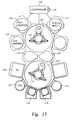
- the integrated process of FIG. 12may be practiced on an integrated tool, such as the Endura tool illustrated in schematic plan view in FIG. 13 and available from Applied Materials, Inc.
- the systemincludes two central vacuum transfer chambers 124 , 126 which are interconnected through vacuum locked pass through stations 128 , 130 and each of which contains a wafer robot 132 , 134 capable of reaching any of multiple stations arranged around the periphery of the respective transfer chambers 124 , 126 .
- Wafersare loaded into and out of the first transfer chamber 124 through wafer cassettes contained in load lock chambers 136 , 138 .
- an orient/degas chamber 142rotates the wafer to the correct orientation and heats it sufficiently to degas it.
- a pre-clean chamber 144then subjects the wafer to an argon plasma pre-cleaning.
- a CVD chamber 148deposits the CVD barrier layer.
- a PVD chamber 150may be used for both PVD steps, both the first one operating to remove material on the via bottom and a second one with a lower ion energy to produce net deposition. If desired, the same chamber can be used for reactive sputtering of a nitrided barrier layer.
- the PVD chamber 150typically has a tantalum target.
- a second PVD chamber 152is used to deposit the copper seed layer.
- the wafer with its liner layer completely formedis returned through the first transfer chamber 124 to a cassette in one of the load locks 136 , 138 . It is appreciated that for higher throughput the empty space on the second transfer chamber 126 can be used for a second CVD barrier chamber 148 or a second PVD barrier chamber 150 depending on their relative processing rates.
- a controller 154is loaded with a process recipe through a removable recording medium 156 and controls the operation of the entire integrated tool.
- ALDAtomic layer deposition
- a first sputtered barrier layermay comprise a first refractory metal
- a second sputtered barrier layermay comprise a second refractory metal requiring another sputter reactor.
- barrier layersmay be based on different materials than those discussed.
- the most common barriersare based on the refractory metals titanium, tantalum, and tungsten and their nitrides, but other barriers are possible.
- the same sputtering chambercan be used for distinctly different effects of removing restricted portions of a liner layer as well as coating over the liner layer and other exposed portions.
Landscapes
- Engineering & Computer Science (AREA)
- Physics & Mathematics (AREA)
- General Physics & Mathematics (AREA)
- Condensed Matter Physics & Semiconductors (AREA)
- Manufacturing & Machinery (AREA)
- Computer Hardware Design (AREA)
- Microelectronics & Electronic Packaging (AREA)
- Power Engineering (AREA)
- General Chemical & Material Sciences (AREA)
- Chemical Kinetics & Catalysis (AREA)
- Chemical & Material Sciences (AREA)
- Plasma & Fusion (AREA)
- Internal Circuitry In Semiconductor Integrated Circuit Devices (AREA)
Abstract
Description
The invention relates generally to processes for formation of vertical interconnects in integrated circuits. In particular, the invention relates to the use of a plasma sputter reactor for both etching and deposition.
Modem integrated circuits include several levels of metallization formed over the active semiconductor circuitry formed in the substrate, most commonly a silicon wafer. The multiple metallization layers are required to interconnect the millions to tens of millions of discrete semiconductor devices formed in a single integrated circuit. For advanced microprocessors, there may be five or more levels of metallization.
Each metallization layer includes a dielectric layer, for example, of silicon dioxide or possibly a low-k dielectric material deposited over the previous layer, a via (or contact) hole etched through the dielectric layer, and a metallization including a vertical metallic plug filled into the hole and a horizontal interconnect formed on top of the dielectric layer.
The formation of vias has become increasingly crucial with the continuing shrinkage of critical dimensions and the transition to copper rather than aluminum interconnects. Contacts to underlying silicon will for the most part not be explicitly described hereafter but can equally benefit from the various aspects of the invention.
A generic via is illustrated in the cross-sectional view of FIG.1. It includes a lower dielectric layer12 (which in the case of a contact is a silicon-containing layer) having formed therein aconductive feature 14, such as another metallization or, in the case of a contact, a contact region of a transistor. An upper leveldielectric layer 16 overlies the lowerdielectric layer 12 and theconductive feature 14. Advanced plasma etching processes etch avia hole 18 through the upperdielectric layer 16 to the vicinity of theconductive feature 14. This explanation avoids many details about etch stop layers, horizontal interconnects, and advanced structures, particularly including dual damascene, but the fundamental concepts for the invention remain the same.
Prior to filling metallization into thevia hole 18, the hole is lined with abarrier layer 20 to prevent the diffusion of aluminum or copper into the dielectric16, which would short out the dielectric between neighboring via, or the diffusion of oxygen from the dielectric16 into the metallization, which reduces the conductivity of the plug. Only thereafter is ametallization plug 22 filled into thevia hole 18. In the case of copper metallization, the filling process typically includes a physical vapor deposition or sputtering (PVD) deposition of a copper seed layer followed by an electrochemical plating (ECP) of copper into the hole.
The barrier structure has become increasingly important as the lateral critical dimension has shrunk to 0.25 μm and below while the vertical dimension has remained virtually static at between 0.7 and 1.5 μm. As a result, the aspect ratio of thevia hole 18 has increased, and the electrical resistance of the vertical electrical metallization has become increasingly important. This emphasis on reduced vertical impedance has been further heightened by the substitution of copper for aluminum as the most desired metallization since copper has a lower bulk resistivity. However, the controlling parameter is the total resistance along a path, including the resistance through the bottombarrier layer portion 24 at the bottom of thevia 18. Particularly in the case of an inter-metal dielectric between two metallizations of the same metal, there is no need to include the bottombarrier layer portion 24 since the copper or other metal in thevia 18 will be contacting a same metal in theconductive feature 14.
In U.S. Pat. No. 5,985,762, Geffken et al. have disclosed directionally etching away the barrier layer exposed on horizontal surfaces of a copper dual-damascene structure but leaving the barrier layer on the sidewalls to protect the dielectric sidewalls from copper sputtered from the underlying copper feature. This process requires presumably a separate etching chamber. Furthermore, the process deleteriously also removes the barrier at the bottom of the trench in a dual-damascene structure. They accordingly deposit another conformal barrier layer, which remains under the metallized via.
In commonly assigned U.S. patent application, Ser. No. 09/518,180 filed Mar. 2, 2000, Gopalraja et al. have suggested that a self-ionized plasma sputter deposition of a copper seed layer for acopper metallization 22 can be used to remove the bottombarrier layer portion 24.
Accordingly, it is desired to provide a structure and method of making it which reduces the contact resistance at the bottom of a via.
It is further desired to provide such structure and method without unduly complicating the integrated circuit fabrication process.
One aspect of the invention includes removing a barrier layer formed at the bottom of a via by a sputter etching process performed in a plasma sputter deposition chamber. The same sputter deposition chamber may advantageously be used to then deposit a second barrier layer.
The invention also includes the aspect of removing the barrier layer at the bottom of the via and simultaneously depositing a second barrier layer on vertically extending sidewalls.
Another aspect of the invention includes removing the barrier layer at the bottom of the via while not removing the barrier layer from some other horizontally extending surfaces. The selective removal can be effected by simultaneously sputter depositing a second barrier layer on these other horizontal surfaces. The selective deposition of the second barrier layer can be advantageously followed by the sputter deposition in the same sputter reactor of another layer of the second barrier layer under different conditions such that the additional layer is also deposited on the via bottom.
The combined process may be performed in an inductively coupled plasma sputter reactor in which, during the removal step, the sputtering target is not energized and thus not sputtered, but, during the deposition of the second barrier layer, it is energized to be sputtered. During the removal step, the inductive coil generates a plasma of the sputtering working gas, and the wafer is biased to attract the working gas ions.
The invention includes structures achievable by the invention in which a barrier layer is coated on the sides of the hole but not its bottom. It also includes a dual-damascene structure in which the barrier is coated on the trench floor but not on the via bottom.
FIG. 1 is a cross-sectional view of a generic via structure of the prior art.
FIG. 2 is a cross-sectional view of a via structure coated with a CVD barrier layer.
FIG. 3 is a cross-sectional view of the via structure of FIG. 2 with the bottom portion of the CVD barrier layer being removed in a PVD chamber.
FIG. 4 is a cross-sectional view of the via structure of FIG. 3 further coated with a PVD barrier layer.
FIG. 5 is a cross-sectional view of the via structure of FIG. 4 coated with a copper seed layer and then electro-chemically filled with copper.
FIG. 6 is a cross-sectional view of the vis structure of FIG. 5 after completion of the inter-level dielectric level by chemical mechanical polishing.
FIG. 7 is a cross-sectional view of a via structure with the CVD barrier being removed from the bottom of the via at the same time that a first PVD barrier layer is deposited at least on the via sidewalls and possibly in the field area over the top of the dielectric.
FIG. 8 is a cross-sectional view of the via structure of FIG. 7 with the further deposition of a second PVD barrier layer.
FIG. 9 is a cross-sectional view of the via structure of FIG. 8 after completion of copper metallization.
FIG. 10 is a cross-sectional view of a dual-damascene structure after deposition of the barrier and seed layers.
FIG. 11 is a cross-sectional view of the structure of FIG. 10 after electroplating and chemical mechanical polishing.
FIG. 12 is a flow diagram of an integrated process liner deposition process.
FIG. 13 is schematic plan view of an integrated tool capable of performing the integrated process of FIG.12.
It has been found useful to form a via barrier in two chambers. The first step is performed in a CVD (chemical vapor deposition) chamber in which aCVD barrier layer 30, as illustrated in the cross-sectional view of FIG. 2, is first deposited having a composition of titanium silicon nitride (TiSiN). Again, the illustrated structure ignores features such as etch stop layers and dual-damascene holes. TheCVD barrier layer 30 may be formed by a three-step process in the T×Z plasma CVD reactor, available from Applied Materials, Inc. of Santa Clara, Calif. Zhao et al. describe a version of this chamber and a TiN deposition procedure in U.S. Pat. No. 5,846,332. In the first step, a TiN layer is deposited to a thickness of about 5mn by a well known process of thermal chemical vapor deposition at about 350° C. using tetrakis-dimethyl-amido titanium (TDMAT) as the precursor gas. Koai et al. describe an alternative plasma CVD process and chamber in U.S. Pat. No. 6,106,625. The thermal CVD is followed by a plasma treatment in the same chamber of the wafer held at 350° C. The same chamber is used for the third step of a thermal soak of the wafer in the presence of silane (SiH4) to convert the TiN to TiSiN. The CVD process is nearly conformal and coats the sidewalls and bottom of the via hole including a CVDbarrier bottom portion 32, a CVDbarrier sidewall portion 34, and a CVDbarrier field portion 36 on top of thedielectric layer 16.
Following the formation of theCVD barrier layer 20, the substrate is transferred to a physical vapor deposition (PVD) chamber in which a tantalum target is used as the sputtering target. The PVD chamber should be one which is capable of producing a relatively high ionization fraction of sputtered atoms, for example, above 10%. The chamber preferably also has the capability of biasing the pedestal electrode supporting the electrode. Typically, the biasing involves applying an RF bias signal, for example, at 13.56 MHz to the pedestal electrode. The RF power creates a negative DC bias on the pedestal and thus accelerates positively charged sputtered metal ions to the wafer.
One reactor satisfying these requirements is the Endura IMP (ion metal plating) sputter reactor available from Applied Materials. This reactor uses an inductive coil to couple RF power into a remote plasma source region. This reactor operates at relatively high argon pressures of about 20 milliTorr to produce a large volume of a high-density plasma, that is, one having an ionization fraction of at least 1011cm−3. Metal ionization fractions may exceed 50% or even 75% in an IMP reactor.
Two other reactors being developed by Applied Materials can also be used for the process of the invention. Both are more conventional DC diode magnetron reactors not relying on RF inductive coupling to create the plasma. Various techniques are used to create a relatively high density plasma in a small portion of the target. The magnetron is scanned over the back of target to provide the required uniformity. Both these reactors can be operated at relatively low pressures of about 1 milliTorr or somewhat less. Their metal ionization fractions are somewhat lower, in the 10% to 50% range. Fu described an SIP (self-ionized plasma) reactor in U.S. patent application Ser. No. 09/373,097, filed Aug. 12, 1999, now issued as U.S. Pat. No. 6,183,614. This reactor uses a flat target and a small unbalanced magnetron having a strong magnet pole of one polarity surrounding a weaker magnetic pole of the other polarity. Praburam et al. describe an SIP+ reactor in U.S. patent application Ser. No. 09/518,180, filed Mar. 2, 2000, now issued as U.S. Pat. No. 2,277,249. This reactor includes a target having a large annular groove or vault formed in its side facing the wafer. Various magnets are placed adjacent to the sidewalls and roof of the vault. Very high plasma densities are formed within portions of the vault, thereby increasing the metal ionization fraction.
According to the invention, the same PVD chamber performs two steps. The first step has the effect of removing the CVD barrier layer at the bottom of the via hole, and the second step completes the deposition of the PVD barrier layer. Two embodiments of the two-step process will be described. In the first, the first step deposits no material and only sputters the CVD barrier layer. In the second, the first step combines removal at the bottom of the via hole and deposition of some PVD barrier material in areas other than the bottom of the via hole.
In the first embodiment, particularly as practiced in an IMP chamber configured for sputter deposition of a barrier layer, an argon plasma is formed and the pedestal electrode is RF biased to create a significant negative DC self-bias to strongly attract the argon ions to the pedestal. The IMP chamber allows the formation of an argon plasma without sputtering the tantalum target by exciting the plasma through the inductive coil and not significantly DC biasing the target. The highly directional high-energy argon ions incident on the wafer remove or sputter the CVD barrier bottom andfield portions barrier sidewall portion 34, as illustrated in the cross-sectional view of FIG. 3, because the ions are mostly traveling parallel to the sidewall. In fact, some of the barrier material sputtered from the CVDbarrier bottom portion 32 will deposit on the sidewall. Further, the argon ions may even slightly etch into the exposedface 38 of the underlyingmetallic feature 14. The etching of themetallic feature 14 may be advantageous as a pre-cleaning step to remove any oxide that has spontaneously formed there. The removal of the CVDbarrier bottom portion 32 at the bottom of the viahole 18 is advantageous because the TiSiN CVD bottom barrier would increase the contact resistance between the plug to be formed in the viahole 18 and the conductive feature. Gopalraja et al. have described in the above cited patent application a similar sputter removal of a barrier layer during sputter deposition of a copper seed layer.
Thereafter, in a second step performed in the same barrier PVD reactor, aPVD barrier layer 40 is sputter deposited, with the chamber conditions adjusted to produce a sufficiently high energy in the sputtered metal ions that they coat not only the top of thedielectric layer 16 but also over theCVD barrier layer 30 on the sidewalls of the via hole18 (although the sidewall coverage is small), and at the bottom of the viahole 18 in direct contact to themetallic feature 14. The second step preferably at least begins with the sputter deposition of tantalum or other barrier metal. The second step may include a subsequent deposition of tantalum nitride by admitting nitrogen into the plasma reactor to effect reactive sputtering.
Exemplary process conditions for the two steps are presented in TABLE 1 for the IMP reactor.
| TABLE 1 | |||
| Target Power | 0 | 1 | ||
| (kW) | ||||
| 1 | 2.5 | |||
| (kW) | ||||
| 1 | 38 | |||
| (milli Torr) | ||||
| Wafer Bias Power | 600 | 350 | ||
| (W) | ||||
| 100 | 50 | |||
| (%) | ||||
These parameters show that the IMP chamber is being operated in the wafer pre-clean mode in the first step and in an ionized sputter deposition mode in the second step.
The wafer is then moved to a copper PVD chamber for deposition of a thincopper seed layer 44, illustrated in the cross-sectional view of FIG.5. Thecopper seed layer 44 is needed to act as an electrode for the subsequent electrochemical plating (ECP) of copper and to nucleate the ECP copper. Thecopper seed layer 44 is preferably performed in either an IMP reactor, a SIP reactor, or a SIP+ reactor although other sputter reactors may be satisfactory. Thereafter, the via hole is filled and overfilled with acopper layer 46 deposited by an ECP process. The excess copper as well as most typically the field portions of the various barriers are removed by chemical mechanical polishing (CMP), which stops on thehard dielectric 16 to produce the structure of FIG.6. It is assumed that a dual-damascene or similar interconnect structure is used so that the remainingmetal 48 acts both as a via to the underlyingmetallic feature 14 and as a horizontal interconnect just below the surface of thedielectric layer 16.
In the SIP and SIP+ sputter reactors as currently configured as well as in other typical diode reactors, the target needs to be powered to create a plasma. In the case of a Ta/TaN barrier, tantalum is being sputtered from the target in the first step. However, it is possible to divide the tantalum sputtering into two steps, the first producing tantalum ions having high energy, the second producing tantalum ions having lower energy so that the first step operates in the sputter removal mode with respect to the wafer while the second step operates in the sputter deposition mode. But, the geometry of the via hole makes the situation more complex.
In the first step, chamber conditions are adjusted to produce tantalum ions having relatively high energies as they are attracted to the wafer to deposit, as illustrated in the cross-sectional view of FIG. 7, a firstPVD barrier layer 70, typically of tantalum for copper metallization. As a result, the ions that are attracted to the bottom of the via18 have such high energy that, not only do they not deposit on the bottom, they sputter away the underlying CVDbarrier bottom portion 32 of FIG.2 and may even slightly etch into the exposedface 38 of the underlyingmetallic feature 14. With the finite tantalum ion flux, asidewall portion 74 of the firstPVD barrier layer 70 is formed on the sides of the viahole 18, partially from the metal ions reflected off the via bottom. The situation in the field area atop thedielectric layer 16 is more complex. If the tantalum ion fraction is high and the ion energy is sufficiently high, then the field portions of the firstPVD barrier layer 70 does not form and instead thefield portion 36 of the CVD barrier is removed. However, in SIP and SIP+ sputtering, it is possible to balance the ion and neutral fractions. The neutral fraction does not reach the protected bottom of the via hole but does reach the field region with modest energy because they are not affected by pedestal biasing. Therefore, they can deposit on the field region more quickly than the energetic ions are removing material there. Therefore, it is possible to achieve a net deposit of the firstPVD barrier layer 70 over the field area. Gopalraja et al. have described in the above cited patent application a similar sputter removal of a barrier layer during sputter deposition of a copper seed layer.
Thereafter, in a second step of the PVD barrier deposition, a secondPVD barrier layer 80, illustrated in FIG. 8, is deposited in the same PVD chamber with the chamber conditions adjusted to produce a lower energy for the sputtered metal ions. With the lower energies, the secondPVD barrier layer 80 forms with abottom portion 82, asidewall portion 84, and afield portion 86. The second step preferably at least begins with the sputter deposition of tantalum or other barrier metal. The second step may include a subsequent deposition of titanium nitride by admitting nitrogen into the plasma reactor to effect reactive sputtering.
Several methods are available to control the metal ion energy. Increasing the RF bias applied to the pedestal electrode through a coupling capacitor will increase the magnitude of the negative DC self-bias and thus increase the energy of the metal ions. At least in the case of SIP and SIP+, either decreasing the chamber pressure or increasing the target power will also increase the DC self-bias. Thus, the second PVD sputtering (deposition) step should be performed at lower bias power, higher pressure, or lower target power than is the first PVD sputtering (etch) step. Of course, adjustment of some combination of the three controls can be used.
The previously described steps associated with deposition of the copper seed layer, electroplating of copper, and chemical mechanical polishing are similarly performed to produce the structure of FIG. 9, which differs from that of FIG. 6 by the addition of the sidewall portion of the firstPVD barrier layer 70.
The SIP and SIP+ sputter reactors allow tuning of not only the metal ion energy but the ratio of ions to neutrals. This tunability allows the possibility of very selective removal of the first barrier layer at only the bottom of the via in a dual-damascene structure, as illustrated in the cross-sectional view of FIG. 10. A multi-step etching process is used to etch a dual-damascene hole in theupper dielectric layer 16 including a viahole 90 for connecting to theunderlying copper feature 14 and atrench 92 providing horizontal interconnects. Usually, there are multiple viaholes 90 and corresponding underlying copper features14. Theunderlying copper feature 14 may be a copper-filled trench in the lower metallization level. Thetrench 92 may have a lateral size only slightly larger than the diameter of the viahole 90, but it typically has a substantially longer length. Etch stop layers and underlying barrier layers are not illustrated.
TheCVD barrier layer 30 is conformally deposited over the horizontal and vertical surfaces of the viahole 90 andtrench 92 as well as over the field area on top of theupper dielectric layer 16. A first PVD sputtering step with energetic metal ions is used to remove theCVD barrier layer 30 at the bottom of the via holes while depositing a firstPVD barrier layer 70 over theCVD barrier layer 30 on the viasidewall 94, thetrench floor 96, the trench sidewalls98, andfield area 100 on top of thedielectric layer 16. The differential deposition, particularly on horizontal surfaces, can be achieved because the very narrow access to the high-aspect ratio viahole 90 admits very few neutral metal atoms to the bottom of the viahole 90, and instead the energetic metal ions etch theCVD barrier layer 30 at the via bottom. On the other hand, thetrench floor 96 is slightly more exposed in its lateral direction and significantly more exposed in it axial direction. As a result, a substantial number of the neutral metal atoms reach thetrench floor 96 and attempt to deposit there. On net, the deposited neutrals prevent the energetic metal ions from significant etching the underlyingCVD barrier layer 30 on thetrench floor 96. The field areas of theCVD barrier layer 30 are even more exposed to the neutral metal atoms, and a thicker firstPVD barrier layer 70 grows there. A second PVD sputter step preferably performed in the same PVD chamber coats a secondPVD barrier layer 80 over the entire exposed surface, including the bottom of the viahole 90.
Gopalraja et al. describe a similar sputter etch and sputter deposition process in U.S. application, Ser. No. 09/703,601, concurrently filed on Nov. 1, 2000 MODES, incorporated herein by reference in its entirety.
Thereafter, the copper seed layer (not illustrated here) is deposited, copper is electroplated into the via and trench and over the top of the trench, and the structure is chemical-mechanically polished down to thedielectric layer 16 to produce the metallized dual-damascene structure of FIG. 11, in which acopper metallization 102 fills both the via90 and thetrench 92. This structure is advantageous over that possible with the barrier removal of Geffken et al. in that the trench floor is protected by a complete set of barrier layers preventing vertical diffusion between theoxide layer 16 andcopper metallization 102.
The steps described above are part of an integrated process for forming a liner in hole penetrating through a dielectric layer. The process flow is presented in the flow diagram of FIG.12 and can be performed on a single integrated tool such as that illustrated in FIG.13. Before entering the system, the via hole is etched through the uppermost dielectric layer down to the underlying metallic feature. The etch may form a dual-damascene structure and involve a more complex structure for the dielectric layer. After the wafer enters the system, instep 110 the wafer is degassed. This operation is usually combined with an orientation step to orient the orientation indicia on the wafer in a predetermined direction. Instep 112, the wafer is pre-cleaned by a process including subjecting the wafer to an argon plasma formed by a remote inductive coil with a chamber pressure of about 0.5 Torr with about 300W of RF bias applied to the pedestal electrode. This soft plasma etch removes spontaneous oxidation and other contaminants from the exposed surface.
Instep 114, a CVD barrier layer is deposited, typically composed of TiN or TiSiN. As described before, the CVD barrier layer nearly conformally coats the sidewalls and bottom of the via hole as well as the field area on top of the dielectric layer.
Step116 is a PVD operation that removes the CVD barrier layer at the bottom of the via. Depending upon the sputter chamber being used and the precise process parameters, the first PVD barrier sputter step may coat a first PVD barrier layer on the via sidewalls and possibly on the field area. In a process tuned for dual damascene the first barrier PVD step removes the CVD barrier layer only at the bottom of the via hole but coats the first PVD barrier layer on the trench floor and in the field area. Step118 sputter deposits another PVD barrier layer on all exposed surfaces including the via bottom, via sidewalls, and field area as well into surfaces of the trench or trenches if any. For a copper metallization, if the first barrier PVD step116 net deposits the barrier, it is preferably a metallic tantalum deposition. In either case, at least an initial part of the PVD barrier layer deposited in the secondbarrier PVD step 118 is preferably composed of tantalum. Optionally, a second part of the second PVD barrier layer is composed of tantalum nitride formed by admitting nitrogen into the PVD reactor. The two barrier PVD steps116,118 are preferably performed in the same plasma sputter reactor having a tantalum or other barrier metal target.
Finally, a copper seed layer is deposited instep 120, after which the wafer having a complete liner formed thereon is removed from the system. Subsequent steps of electro-chemical plating (ECP) and chemical mechanical polishing (CMP) are performed elsewhere to complete the inter-level metallization. It is also appreciated that the invention does not require ECP or CMP, but may instead use more conventional sputter filling of the via and/or metal lithography of the horizontal interconnects. It is further appreciated that the liner process is not restricted to copper metallization, and the process may be adapted to aluminum metallization.
The integrated process of FIG. 12 may be practiced on an integrated tool, such as the Endura tool illustrated in schematic plan view in FIG.13 and available from Applied Materials, Inc. The system includes two centralvacuum transfer chambers stations wafer robot respective transfer chambers
Wafers are loaded into and out of thefirst transfer chamber 124 through wafer cassettes contained inload lock chambers degas chamber 142 rotates the wafer to the correct orientation and heats it sufficiently to degas it. Apre-clean chamber 144 then subjects the wafer to an argon plasma pre-cleaning.
The wafer is then transferred to thesecond transfer chamber 126, which is typically held at a higher vacuum than thefirst transfer chamber 124. ACVD chamber 148 deposits the CVD barrier layer. APVD chamber 150 may be used for both PVD steps, both the first one operating to remove material on the via bottom and a second one with a lower ion energy to produce net deposition. If desired, the same chamber can be used for reactive sputtering of a nitrided barrier layer. For copper metallization, thePVD chamber 150 typically has a tantalum target. Asecond PVD chamber 152 is used to deposit the copper seed layer. Thereafter, the wafer with its liner layer completely formed is returned through thefirst transfer chamber 124 to a cassette in one of the load locks136,138. It is appreciated that for higher throughput the empty space on thesecond transfer chamber 126 can be used for a secondCVD barrier chamber 148 or a secondPVD barrier chamber 150 depending on their relative processing rates.
Acontroller 154 is loaded with a process recipe through a removable recording medium156 and controls the operation of the entire integrated tool.
Although the invention has been described in context of the first barrier layer being deposited by a CVD method, the invention is applicable to structures using first barrier layers deposited by other methods. Atomic layer deposition (ALD) is a process for depositing the barrier one atomic layer at a time. In another example, a first sputtered barrier layer may comprise a first refractory metal, and a second sputtered barrier layer may comprise a second refractory metal requiring another sputter reactor.
It is appreciated that the various barrier layers may be based on different materials than those discussed. The most common barriers are based on the refractory metals titanium, tantalum, and tungsten and their nitrides, but other barriers are possible.
Accordingly, it is seen that the same sputtering chamber can be used for distinctly different effects of removing restricted portions of a liner layer as well as coating over the liner layer and other exposed portions.
Claims (31)
1. A process performed in a plasma sputter reactor having a metal target for forming a barrier in a hole formed in a dielectric layer formed over a substrate, wherein a first barrier layer is coated on a bottom and on sidewalls of said hole, said process comprising the steps of:
a first step performed in said plasma sputter reactor of sputtering said first barrier layer from said bottom of said hole; and
a second step performed in said plasma sputter reactor of sputter depositing from said target a second barrier layer over a bottom of said hole and over said first barrier layer on said sidewalls of said hole;
wherein said first and second barrier layers act as barriers to diffusion between said dielectric layer and metal filled into said hole.
2. The process ofclaim 1 , wherein said second step additionally deposits a barrier layer on sidewalls of said hole.
3. The process ofclaim 1 ,
wherein said first and second steps are performed in a plasma sputter chamber having an inductive coil coupling RF energy into said chamber;
wherein said first step is performed while coupling RF energy into said chamber to excite a plasma of argon but while not negatively biasing said target to a sufficient degree to sputter said target to coat said bottom of said hole; and
wherein said second step is performed while negatively biasing said target to effect sputtering of said target.
4. The process ofclaim 1 ,
wherein said first and second steps are performed in a diode plasma chamber; and
wherein a DC self-bias applied to a pedestal electrode supporting said substrate is greater in said first step than in said second step.
5. The process ofclaim 1 ,
wherein said first and second steps are performed in a diode plasma chamber; and
wherein a pressure in said chamber is less in said first step than in said second step.
6. The process ofclaim 1 ,
wherein said first and second steps are performed in a diode plasma chamber; and
wherein greater power is applied to said metal target in said second step than in said first step.
7. The process ofclaim 1 , further comprising depositing a copper seed layer over said second barrier layer.
8. The process ofclaim 7 , further comprising electrochemically filling said hole with copper.
9. The process ofclaim 1 , wherein during said first and second steps said substrate is in opposition to said target.
10. The process ofclaim 1 , wherein said second step includes reactive sputtering of a metal nitride.
11. The process ofclaim 10 , wherein said metal nitride comprises tantalum nitride.
12. A process for forming a barrier in a hole formed in a dielectric layer formed over a substrate, wherein a first barrier layer is coated on a bottom and on sidewalls of said hole, said process comprising the steps of:
a first step performed in a plasma sputter reactor having a metal target of sputtering said first barrier layer from said bottom of said hole, wherein said first step leaves said barrier layer exposed on said sidewalls of said hole; and
a second step performed in said plasma sputter reactor of sputter depositing from said metal target a second barrier layer over a bottom of said hole and over said first barrier layer on said sidewalls of said hole;
wherein said first and second barrier layers act as barriers to diffusion between said dielectric layer and metal filled into said hole.
13. The process ofclaim 12 ,
wherein said barrier layer is coated over a top of said dielectric layer;
wherein said first step removes said first barrier layer from said top of said dielectric layer; and
wherein said second step deposits said second barrier layer over said top of said dielectric layer.
14. The process ofclaim 12 , wherein a pedestal electrode supporting said substrate is impressed with a larger negative bias in said second step than in said first step.
15. The process ofclaim 12 , wherein a pressure in a chamber of said reactor containing said target and said substrate is lower in said first step than in said second step.
16. The process ofclaim 12 , wherein a power applied to said target in said reactor is higher in said second step than in said first step.
17. The process ofclaim 12 ,
wherein said second barrier layer includes a nitride portion at said bottom of said via hole, and
further comprising sputter coating a copper seed layer over said sidewalls of said via hole while simultaneously removing said nitride portion.
18. A process for forming a barrier in a hole formed in a dielectric layer formed over a substrate, comprising the steps of:
a first step of depositing a first barrier layer on a bottom and on sidewalls of said hole; and
a second step of simultaneously depositing a second barrier layer on said sidewalls while removing said first barrier layer from said bottom.
19. A process for forming a barrier in a hole formed in a dielectric layer formed over a substrate, comprising the steps of:
a first step of depositing a first barrier layer on a bottom and on sidewalls of said hole;
a second step of simultaneously depositing a second barrier layer on said sidewalls while removing said first barrier layer from said bottom; and
a third step of depositing a third barrier layer on said bottom and said sidewalls,
wherein said first, second and third barrier layers deposited on said sidewalls act as a diffusion barrier between metal filled into said hole and said dielectric layer.
20. The process ofclaim 19 , wherein said second and third barrier layers comprise a same metal.
21. The process ofclaim 20 , wherein said same metal is tantalum.
22. The process ofclaim 19 , wherein said second and third steps are performed in a same plasma sputter reactor.
23. The process ofclaim 19 , wherein said second step produces metal ions having higher energies than does said third step.
24. The process ofclaim 19 , wherein a pedestal electrode supporting said substrate is impressed with a larger negative bias in said second step than in said third step.
25. The process ofclaim 19 , wherein a pressure in said chamber is lower in said second step than in said third step.
26. The process ofclaim 19 , wherein a power applied to a target in said reactor is lower in said second step than in said third step.
27. The process ofclaim 18 , wherein said first barrier layer comprises titanium and nitrogen.
28. The process ofclaim 18 , wherein said first step comprises chemical vapor deposition and said second step is performed in a plasma sputter reactor.
29. The process ofclaim 18 , wherein said second barrier layer comprises a metal nitride layer.
30. The process ofclaim 29 , wherein said metal nitride layer comprises tantalum nitride.
31. A process for forming a barrier in a hole formed in a dielectric layer formed over a substrate, wherein a first barrier layer is coated on a bottom and on sidewalls of said hole, said process comprising the steps of:
sputtering said first barrier layer from said bottom of said hole; and
sputter depositing a second barrier layer over a bottom of said hole and over said first barrier layer on said sidewalls of said hole;
wherein said sputtering step and said sputter depositing step are performed in a same plasma reactor and wherein said first and second barrier layers act as barriers to diffusion between said dielectric layer and metal filled into said hole.
Priority Applications (6)
| Application Number | Priority Date | Filing Date | Title |
|---|---|---|---|
| US09/704,161US6498091B1 (en) | 2000-11-01 | 2000-11-01 | Method of using a barrier sputter reactor to remove an underlying barrier layer |
| TW090127096ATW521379B (en) | 2000-11-01 | 2001-10-31 | Use of a barrier sputter reactor to remove an underlying barrier layer |
| PCT/US2001/045167WO2002039500A2 (en) | 2000-11-01 | 2001-11-01 | Use of a barrier sputter reactor to remove an underlying barrier layer |
| US10/290,746US6660622B2 (en) | 2000-11-01 | 2002-11-07 | Process for removing an underlying layer and depositing a barrier layer in one reactor |
| US10/693,775US6953742B2 (en) | 2000-11-01 | 2003-10-25 | Tantalum barrier layer for copper metallization |
| US11/184,431US7576002B2 (en) | 2000-11-01 | 2005-07-19 | Multi-step barrier deposition method |
Applications Claiming Priority (1)
| Application Number | Priority Date | Filing Date | Title |
|---|---|---|---|
| US09/704,161US6498091B1 (en) | 2000-11-01 | 2000-11-01 | Method of using a barrier sputter reactor to remove an underlying barrier layer |
Related Child Applications (2)
| Application Number | Title | Priority Date | Filing Date |
|---|---|---|---|
| US10/290,746ContinuationUS6660622B2 (en) | 2000-11-01 | 2002-11-07 | Process for removing an underlying layer and depositing a barrier layer in one reactor |
| US10/290,746DivisionUS6660622B2 (en) | 2000-11-01 | 2002-11-07 | Process for removing an underlying layer and depositing a barrier layer in one reactor |
Publications (1)
| Publication Number | Publication Date |
|---|---|
| US6498091B1true US6498091B1 (en) | 2002-12-24 |
Family
ID=24828340
Family Applications (4)
| Application Number | Title | Priority Date | Filing Date |
|---|---|---|---|
| US09/704,161Expired - LifetimeUS6498091B1 (en) | 2000-11-01 | 2000-11-01 | Method of using a barrier sputter reactor to remove an underlying barrier layer |
| US10/290,746Expired - LifetimeUS6660622B2 (en) | 2000-11-01 | 2002-11-07 | Process for removing an underlying layer and depositing a barrier layer in one reactor |
| US10/693,775Expired - LifetimeUS6953742B2 (en) | 2000-11-01 | 2003-10-25 | Tantalum barrier layer for copper metallization |
| US11/184,431Expired - Fee RelatedUS7576002B2 (en) | 2000-11-01 | 2005-07-19 | Multi-step barrier deposition method |
Family Applications After (3)
| Application Number | Title | Priority Date | Filing Date |
|---|---|---|---|
| US10/290,746Expired - LifetimeUS6660622B2 (en) | 2000-11-01 | 2002-11-07 | Process for removing an underlying layer and depositing a barrier layer in one reactor |
| US10/693,775Expired - LifetimeUS6953742B2 (en) | 2000-11-01 | 2003-10-25 | Tantalum barrier layer for copper metallization |
| US11/184,431Expired - Fee RelatedUS7576002B2 (en) | 2000-11-01 | 2005-07-19 | Multi-step barrier deposition method |
Country Status (3)
| Country | Link |
|---|---|
| US (4) | US6498091B1 (en) |
| TW (1) | TW521379B (en) |
| WO (1) | WO2002039500A2 (en) |
Cited By (418)
| Publication number | Priority date | Publication date | Assignee | Title |
|---|---|---|---|---|
| US20020060363A1 (en)* | 1997-05-14 | 2002-05-23 | Applied Materials, Inc. | Reliability barrier integration for Cu application |
| US20020089063A1 (en)* | 2001-01-08 | 2002-07-11 | Ahn Kie Y. | Copper dual damascene interconnect technology |
| EP1233448A3 (en)* | 2001-02-14 | 2003-04-23 | Texas Instruments Inc. | Reliable interconnects with low via/contact resistance |
| US20030075752A1 (en)* | 2001-10-19 | 2003-04-24 | Nec Corporation | Semiconductor device and method for manufacturing the same |
| US20030116427A1 (en)* | 2001-08-30 | 2003-06-26 | Applied Materials, Inc. | Self-ionized and inductively-coupled plasma for sputtering and resputtering |
| US6620724B1 (en)* | 2002-05-09 | 2003-09-16 | Infineon Technologies Ag | Low resistivity deep trench fill for DRAM and EDRAM applications |
| US20040018722A1 (en)* | 2002-07-25 | 2004-01-29 | Matsushita Electric Industrial Co., Ltd. | Method for manufacturing semiconductor device |
| US6689684B1 (en)* | 2001-02-15 | 2004-02-10 | Advanced Micro Devices, Inc. | Cu damascene interconnections using barrier/capping layer |
| US20040048461A1 (en)* | 2002-09-11 | 2004-03-11 | Fusen Chen | Methods and apparatus for forming barrier layers in high aspect ratio vias |
| US20040058527A1 (en)* | 2002-09-20 | 2004-03-25 | Semiconductor Energy Laboratory Co., Ltd. | Manufacturing method of semiconductor device |
| US20040056855A1 (en)* | 2002-09-20 | 2004-03-25 | Semiconductor Energy Laboratory Co., Ltd. | Display device and manufacturing method thereof |
| US20040063307A1 (en)* | 2002-09-30 | 2004-04-01 | Subramanian Karthikeyan | Method to avoid copper contamination of a via or dual damascene structure |
| US20040094402A1 (en)* | 2002-08-01 | 2004-05-20 | Applied Materials, Inc. | Self-ionized and capacitively-coupled plasma for sputtering and resputtering |
| US20040115928A1 (en)* | 2002-12-11 | 2004-06-17 | International Business Machines Corporation | Method for depositing a metal layer on a semiconductor interconnect structure |
| US20040115930A1 (en)* | 2002-12-14 | 2004-06-17 | Dongbu Electronics Co., Ltd. | Method for forming barrier metal of semiconductor device |
| US20040157425A1 (en)* | 2001-10-18 | 2004-08-12 | Lsi Logic Corporation | Multi-step process for forming a barrier film for use in copper layer formation |
| WO2004070830A1 (en)* | 2003-02-03 | 2004-08-19 | International Business Machines Corporation | Sacrificial metal liner for copper interconnects |
| US20040241979A1 (en)* | 2003-05-27 | 2004-12-02 | Texas Instruments Incorporated | Methods for providing improved layer adhesion in a semiconductor device |
| US20040253807A1 (en)* | 2003-06-13 | 2004-12-16 | Taiwan Semiconductor Manufacturing Co., Ltd. | Barrier layer stack to prevent Ti diffusion |
| WO2004114398A1 (en)* | 2003-06-13 | 2004-12-29 | Applied Materials, Inc. | Integration of ald tantalum nitride for copper metallization |
| US20050074968A1 (en)* | 2000-11-01 | 2005-04-07 | Ling Chen | Tantalum barrier layer for copper metallization |
| US20050093155A1 (en)* | 2003-10-31 | 2005-05-05 | Volker Kahlert | Barrier layer including a titanium nitride liner for a copper metallization layer including a low-k dielectric |
| US20050101148A1 (en)* | 2003-11-08 | 2005-05-12 | Advanced Micro Devices, Inc. | Method for preventing an increase in contact hole width during contact formation |
| US20050098427A1 (en)* | 2003-11-11 | 2005-05-12 | Taiwan Semiconductor Manufacturing Co., Ltd. | RF coil design for improved film uniformity of an ion metal plasma source |
| US20050118796A1 (en)* | 2003-11-28 | 2005-06-02 | Chiras Stefanie R. | Process for forming an electrically conductive interconnect |
| US20050181598A1 (en)* | 2003-01-15 | 2005-08-18 | Kailasam Sridhar K. | Methods of providing an adhesion layer for adhesion of barrier and/or seed layers to dielectric films |
| US20050263891A1 (en)* | 2004-05-28 | 2005-12-01 | Bih-Huey Lee | Diffusion barrier for damascene structures |
| US20060009034A1 (en)* | 2000-06-28 | 2006-01-12 | Lai Ken K | Methods for depositing tungsten layers employing atomic layer deposition techniques |
| US20060068604A1 (en)* | 2004-09-30 | 2006-03-30 | Cheng-Lin Huang | Barrier layer and fabrication method thereof |
| US20060073690A1 (en)* | 2004-10-05 | 2006-04-06 | Applied Materials, Inc. | Apparatus and method for metal plasma vapor deposition and re-sputter with source and bias power frequencies applied through the workpiece |
| US20060073283A1 (en)* | 2004-10-05 | 2006-04-06 | Applied Materials, Inc. | Apparatus for metal plasma vapor deposition and re-sputter with source and bias power frequencies applied through the workpiece |
| US20060073700A1 (en)* | 2004-10-05 | 2006-04-06 | Applied Materials, Inc. | Method for forming a barrier layer in an integrated circuit in a plasma with source and bias power frequencies applied through the workpiece |
| US20060081986A1 (en)* | 2004-10-14 | 2006-04-20 | International Business Machines Corporation | Modified via bottom structure for reliability enhancement |
| US7049226B2 (en) | 2001-09-26 | 2006-05-23 | Applied Materials, Inc. | Integration of ALD tantalum nitride for copper metallization |
| US20060169578A1 (en)* | 2005-02-03 | 2006-08-03 | Applied Materials, Inc. | Apparatus for plasma-enhanced physical vapor deposition of copper with RF source power applied through the workpiece with a lighter-than-copper carrier gas |
| US20060194430A1 (en)* | 2005-02-28 | 2006-08-31 | Michael Beck | Metal interconnect structure and method |
| US20060216928A1 (en)* | 2001-12-07 | 2006-09-28 | Hua Chung | Cyclical deposition of refractory metal silicon nitride |
| US20060223300A1 (en)* | 2005-03-31 | 2006-10-05 | Harsono Simka | Organometallic precursors for the chemical phase deposition of metal films in interconnect applications |
| DE102004015862B4 (en)* | 2004-03-31 | 2006-11-16 | Advanced Micro Devices, Inc., Sunnyvale | A method of forming a conductive barrier layer in critical openings by means of a final deposition step after backsputter deposition |
| US20060264048A1 (en)* | 2003-11-21 | 2006-11-23 | International Business Machines Corporation | Interconnect Structure Diffusion Barrier With High Nitrogen Content |
| US20070126120A1 (en)* | 2005-12-06 | 2007-06-07 | Taiwan Semiconductor Manufacturing Co., Ltd. | Semiconductor device |
| US20070152342A1 (en)* | 2005-12-30 | 2007-07-05 | Taiwan Semiconductor Manufacturing Co., Ltd. | Via structure and process for forming the same |
| US20070218688A1 (en)* | 2000-06-28 | 2007-09-20 | Ming Xi | Method for depositing tungsten-containing layers by vapor deposition techniques |
| US20070257366A1 (en)* | 2006-05-03 | 2007-11-08 | Taiwan Semiconductor Manufacturing Company, Ltd. | Barrier layer for semiconductor interconnect structure |
| US20070284736A1 (en)* | 2006-05-18 | 2007-12-13 | International Business Machines Corporation | Enhanced mechanical strength via contacts |
| US20070285471A1 (en)* | 2003-08-25 | 2007-12-13 | Sung-Joon Park | Protective layer of ink-jet print head and method of making ink-jet print head having the same |
| US20080012142A1 (en)* | 2006-02-15 | 2008-01-17 | International Business Machines Corporation | Structure and method of chemically formed anchored metallic vias |
| CN100364057C (en)* | 2004-11-24 | 2008-01-23 | 中芯国际集成电路制造(上海)有限公司 | Method and system for metal barrier and seed integration |
| US20080057700A1 (en)* | 2006-08-31 | 2008-03-06 | Dongbu Hitek Co., Ltd. | Apparatus for manufacturing semiconductor device and method for manufacturing semiconductor device using the same |
| US7352048B2 (en) | 2001-09-26 | 2008-04-01 | Applied Materials, Inc. | Integration of barrier layer and seed layer |
| US20080157371A1 (en)* | 2006-12-27 | 2008-07-03 | Seung Hyun Kim | Metal Line of Semiconductor Device and Method of Manufacturing the Same |
| US20080169189A1 (en)* | 2006-05-16 | 2008-07-17 | Southwest Research Institute | Apparatus And Method for RF Plasma Enhanced Magnetron Sputter Deposition |
| US7402210B2 (en) | 2002-11-14 | 2008-07-22 | Applied Materials, Inc. | Apparatus and method for hybrid chemical processing |
| US20080182409A1 (en)* | 2007-01-31 | 2008-07-31 | Robert Seidel | Method of forming a metal layer over a patterned dielectric by electroless deposition using a selectively provided activation layer |
| US20080237861A1 (en)* | 2007-03-30 | 2008-10-02 | Dominguez Juan E | Novel Fluorine-Free Precursors and Methods for the Deposition of Conformal Conductive Films for Nanointerconnect Seed and Fill |
| CN100424868C (en)* | 2005-07-13 | 2008-10-08 | 精工爱普生株式会社 | Semiconductor device and manufacturing method thereof |
| US7465666B2 (en) | 2000-06-28 | 2008-12-16 | Applied Materials, Inc. | Method for forming tungsten materials during vapor deposition processes |
| US20090045047A1 (en)* | 2007-08-14 | 2009-02-19 | Southwest Research Institute | Conformal Magnetron Sputter Deposition |
| US20090087982A1 (en)* | 2007-09-28 | 2009-04-02 | Applied Materials, Inc. | Selective ruthenium deposition on copper materials |
| US7514358B2 (en) | 2002-03-04 | 2009-04-07 | Applied Materials, Inc. | Sequential deposition of tantalum nitride using a tantalum-containing precursor and a nitrogen-containing precursor |
| US7521379B2 (en) | 2006-10-09 | 2009-04-21 | Applied Materials, Inc. | Deposition and densification process for titanium nitride barrier layers |
| US20090117733A1 (en)* | 2002-06-28 | 2009-05-07 | Dubin Valery M | Protection of seedlayer for electroplating |
| US7585762B2 (en) | 2007-09-25 | 2009-09-08 | Applied Materials, Inc. | Vapor deposition processes for tantalum carbide nitride materials |
| DE102004017411B4 (en)* | 2003-04-09 | 2010-01-07 | Infineon Technologies Ag | In situ metal barrier deposition for sputter etching on a connection structure |
| US7645696B1 (en) | 2006-06-22 | 2010-01-12 | Novellus Systems, Inc. | Deposition of thin continuous PVD seed layers having improved adhesion to the barrier layer |
| US7659197B1 (en) | 2007-09-21 | 2010-02-09 | Novellus Systems, Inc. | Selective resputtering of metal seed layers |
| US7678298B2 (en) | 2007-09-25 | 2010-03-16 | Applied Materials, Inc. | Tantalum carbide nitride materials by vapor deposition processes |
| US7682946B2 (en) | 2005-11-04 | 2010-03-23 | Applied Materials, Inc. | Apparatus and process for plasma-enhanced atomic layer deposition |
| US7682966B1 (en) | 2007-02-01 | 2010-03-23 | Novellus Systems, Inc. | Multistep method of depositing metal seed layers |
| US7732314B1 (en)* | 2001-03-13 | 2010-06-08 | Novellus Systems, Inc. | Method for depositing a diffusion barrier for copper interconnect applications |
| US7732327B2 (en) | 2000-06-28 | 2010-06-08 | Applied Materials, Inc. | Vapor deposition of tungsten materials |
| US7745327B2 (en)* | 2007-01-31 | 2010-06-29 | Advanced Micro Devices, Inc. | Method of forming a copper-based metallization layer including a conductive cap layer by an advanced integration regime |
| US7781327B1 (en) | 2001-03-13 | 2010-08-24 | Novellus Systems, Inc. | Resputtering process for eliminating dielectric damage |
| US7780788B2 (en) | 2001-10-26 | 2010-08-24 | Applied Materials, Inc. | Gas delivery apparatus for atomic layer deposition |
| US7794544B2 (en) | 2004-05-12 | 2010-09-14 | Applied Materials, Inc. | Control of gas flow and delivery to suppress the formation of particles in an MOCVD/ALD system |
| US7798096B2 (en) | 2006-05-05 | 2010-09-21 | Applied Materials, Inc. | Plasma, UV and ion/neutral assisted ALD or CVD in a batch tool |
| US7824743B2 (en) | 2007-09-28 | 2010-11-02 | Applied Materials, Inc. | Deposition processes for titanium nitride barrier and aluminum |
| US7842605B1 (en) | 2003-04-11 | 2010-11-30 | Novellus Systems, Inc. | Atomic layer profiling of diffusion barrier and metal seed layers |
| US7851360B2 (en) | 2007-02-14 | 2010-12-14 | Intel Corporation | Organometallic precursors for seed/barrier processes and methods thereof |
| US7855147B1 (en) | 2006-06-22 | 2010-12-21 | Novellus Systems, Inc. | Methods and apparatus for engineering an interface between a diffusion barrier layer and a seed layer |
| US7897516B1 (en) | 2007-05-24 | 2011-03-01 | Novellus Systems, Inc. | Use of ultra-high magnetic fields in resputter and plasma etching |
| US7922880B1 (en) | 2007-05-24 | 2011-04-12 | Novellus Systems, Inc. | Method and apparatus for increasing local plasma density in magnetically confined plasma |
| US7964505B2 (en) | 2005-01-19 | 2011-06-21 | Applied Materials, Inc. | Atomic layer deposition of tungsten materials |
| US8017523B1 (en) | 2008-05-16 | 2011-09-13 | Novellus Systems, Inc. | Deposition of doped copper seed layers having improved reliability |
| US20110220490A1 (en)* | 2010-03-15 | 2011-09-15 | Southwest Research Institute | Apparatus And Method Utilizing A Double Glow Discharge Plasma For Sputter Cleaning |
| US8043484B1 (en) | 2001-03-13 | 2011-10-25 | Novellus Systems, Inc. | Methods and apparatus for resputtering process that improves barrier coverage |
| US8298933B2 (en) | 2003-04-11 | 2012-10-30 | Novellus Systems, Inc. | Conformal films on semiconductor substrates |
| US8491967B2 (en) | 2008-09-08 | 2013-07-23 | Applied Materials, Inc. | In-situ chamber treatment and deposition process |
| US8668816B2 (en) | 1999-10-08 | 2014-03-11 | Applied Materials Inc. | Self-ionized and inductively-coupled plasma for sputtering and resputtering |
| US8679972B1 (en)* | 2001-03-13 | 2014-03-25 | Novellus Systems, Inc. | Method of depositing a diffusion barrier for copper interconnect applications |
| US8836129B1 (en)* | 2013-03-14 | 2014-09-16 | United Microelectronics Corp. | Plug structure |
| US8858763B1 (en) | 2006-11-10 | 2014-10-14 | Novellus Systems, Inc. | Apparatus and methods for deposition and/or etch selectivity |
| US9082719B2 (en) | 2012-10-19 | 2015-07-14 | Infineon Technologies Ag | Method for removing a dielectric layer from a bottom of a trench |
| US20150240359A1 (en)* | 2014-02-25 | 2015-08-27 | Asm Ip Holding B.V. | Gas Supply Manifold And Method Of Supplying Gases To Chamber Using Same |
| EP2913842A2 (en) | 2008-07-03 | 2015-09-02 | Applied Materials, Inc. | Apparatuses for atomic layer deposition |
| US9418890B2 (en) | 2008-09-08 | 2016-08-16 | Applied Materials, Inc. | Method for tuning a deposition rate during an atomic layer deposition process |
| US10047430B2 (en) | 1999-10-08 | 2018-08-14 | Applied Materials, Inc. | Self-ionized and inductively-coupled plasma for sputtering and resputtering |
| US10559458B1 (en) | 2018-11-26 | 2020-02-11 | Asm Ip Holding B.V. | Method of forming oxynitride film |
| US10561975B2 (en) | 2014-10-07 | 2020-02-18 | Asm Ip Holdings B.V. | Variable conductance gas distribution apparatus and method |
| USD876504S1 (en) | 2017-04-03 | 2020-02-25 | Asm Ip Holding B.V. | Exhaust flow control ring for semiconductor deposition apparatus |
| US10590535B2 (en) | 2017-07-26 | 2020-03-17 | Asm Ip Holdings B.V. | Chemical treatment, deposition and/or infiltration apparatus and method for using the same |
| US10600673B2 (en) | 2015-07-07 | 2020-03-24 | Asm Ip Holding B.V. | Magnetic susceptor to baseplate seal |
| US10604847B2 (en) | 2014-03-18 | 2020-03-31 | Asm Ip Holding B.V. | Gas distribution system, reactor including the system, and methods of using the same |
| US10612136B2 (en) | 2018-06-29 | 2020-04-07 | ASM IP Holding, B.V. | Temperature-controlled flange and reactor system including same |
| US10622375B2 (en) | 2016-11-07 | 2020-04-14 | Asm Ip Holding B.V. | Method of processing a substrate and a device manufactured by using the method |
| US10643904B2 (en) | 2016-11-01 | 2020-05-05 | Asm Ip Holdings B.V. | Methods for forming a semiconductor device and related semiconductor device structures |
| US10643826B2 (en) | 2016-10-26 | 2020-05-05 | Asm Ip Holdings B.V. | Methods for thermally calibrating reaction chambers |
| US10655221B2 (en) | 2017-02-09 | 2020-05-19 | Asm Ip Holding B.V. | Method for depositing oxide film by thermal ALD and PEALD |
| US10658181B2 (en) | 2018-02-20 | 2020-05-19 | Asm Ip Holding B.V. | Method of spacer-defined direct patterning in semiconductor fabrication |
| US10658205B2 (en) | 2017-09-28 | 2020-05-19 | Asm Ip Holdings B.V. | Chemical dispensing apparatus and methods for dispensing a chemical to a reaction chamber |
| US10665452B2 (en) | 2016-05-02 | 2020-05-26 | Asm Ip Holdings B.V. | Source/drain performance through conformal solid state doping |
| US10672636B2 (en) | 2017-08-09 | 2020-06-02 | Asm Ip Holding B.V. | Cassette holder assembly for a substrate cassette and holding member for use in such assembly |
| US10685834B2 (en) | 2017-07-05 | 2020-06-16 | Asm Ip Holdings B.V. | Methods for forming a silicon germanium tin layer and related semiconductor device structures |
| US10692741B2 (en) | 2017-08-08 | 2020-06-23 | Asm Ip Holdings B.V. | Radiation shield |
| US10707106B2 (en) | 2011-06-06 | 2020-07-07 | Asm Ip Holding B.V. | High-throughput semiconductor-processing apparatus equipped with multiple dual-chamber modules |
| US10714350B2 (en) | 2016-11-01 | 2020-07-14 | ASM IP Holdings, B.V. | Methods for forming a transition metal niobium nitride film on a substrate by atomic layer deposition and related semiconductor device structures |
| US10714315B2 (en) | 2012-10-12 | 2020-07-14 | Asm Ip Holdings B.V. | Semiconductor reaction chamber showerhead |
| US10714335B2 (en) | 2017-04-25 | 2020-07-14 | Asm Ip Holding B.V. | Method of depositing thin film and method of manufacturing semiconductor device |
| US10714385B2 (en) | 2016-07-19 | 2020-07-14 | Asm Ip Holding B.V. | Selective deposition of tungsten |
| US10720322B2 (en) | 2016-02-19 | 2020-07-21 | Asm Ip Holding B.V. | Method for forming silicon nitride film selectively on top surface |
| US10720331B2 (en) | 2016-11-01 | 2020-07-21 | ASM IP Holdings, B.V. | Methods for forming a transition metal nitride film on a substrate by atomic layer deposition and related semiconductor device structures |
| US10734497B2 (en) | 2017-07-18 | 2020-08-04 | Asm Ip Holding B.V. | Methods for forming a semiconductor device structure and related semiconductor device structures |
| US10731249B2 (en) | 2018-02-15 | 2020-08-04 | Asm Ip Holding B.V. | Method of forming a transition metal containing film on a substrate by a cyclical deposition process, a method for supplying a transition metal halide compound to a reaction chamber, and related vapor deposition apparatus |
| US10734244B2 (en) | 2017-11-16 | 2020-08-04 | Asm Ip Holding B.V. | Method of processing a substrate and a device manufactured by the same |
| US10734223B2 (en) | 2017-10-10 | 2020-08-04 | Asm Ip Holding B.V. | Method for depositing a metal chalcogenide on a substrate by cyclical deposition |
| US10741385B2 (en) | 2016-07-28 | 2020-08-11 | Asm Ip Holding B.V. | Method and apparatus for filling a gap |
| US10755922B2 (en) | 2018-07-03 | 2020-08-25 | Asm Ip Holding B.V. | Method for depositing silicon-free carbon-containing film as gap-fill layer by pulse plasma-assisted deposition |
| US10755923B2 (en) | 2018-07-03 | 2020-08-25 | Asm Ip Holding B.V. | Method for depositing silicon-free carbon-containing film as gap-fill layer by pulse plasma-assisted deposition |
| US10770286B2 (en) | 2017-05-08 | 2020-09-08 | Asm Ip Holdings B.V. | Methods for selectively forming a silicon nitride film on a substrate and related semiconductor device structures |
| US10767789B2 (en) | 2018-07-16 | 2020-09-08 | Asm Ip Holding B.V. | Diaphragm valves, valve components, and methods for forming valve components |
| US10770336B2 (en) | 2017-08-08 | 2020-09-08 | Asm Ip Holding B.V. | Substrate lift mechanism and reactor including same |
| US10784102B2 (en) | 2016-12-22 | 2020-09-22 | Asm Ip Holding B.V. | Method of forming a structure on a substrate |
| US10787741B2 (en) | 2014-08-21 | 2020-09-29 | Asm Ip Holding B.V. | Method and system for in situ formation of gas-phase compounds |
| US10797133B2 (en) | 2018-06-21 | 2020-10-06 | Asm Ip Holding B.V. | Method for depositing a phosphorus doped silicon arsenide film and related semiconductor device structures |
| US10804098B2 (en) | 2009-08-14 | 2020-10-13 | Asm Ip Holding B.V. | Systems and methods for thin-film deposition of metal oxides using excited nitrogen-oxygen species |
| US10811256B2 (en) | 2018-10-16 | 2020-10-20 | Asm Ip Holding B.V. | Method for etching a carbon-containing feature |
| USD900036S1 (en) | 2017-08-24 | 2020-10-27 | Asm Ip Holding B.V. | Heater electrical connector and adapter |
| US10818758B2 (en) | 2018-11-16 | 2020-10-27 | Asm Ip Holding B.V. | Methods for forming a metal silicate film on a substrate in a reaction chamber and related semiconductor device structures |
| US10829852B2 (en) | 2018-08-16 | 2020-11-10 | Asm Ip Holding B.V. | Gas distribution device for a wafer processing apparatus |
| US10832903B2 (en) | 2011-10-28 | 2020-11-10 | Asm Ip Holding B.V. | Process feed management for semiconductor substrate processing |
| US10847365B2 (en) | 2018-10-11 | 2020-11-24 | Asm Ip Holding B.V. | Method of forming conformal silicon carbide film by cyclic CVD |
| US10847371B2 (en) | 2018-03-27 | 2020-11-24 | Asm Ip Holding B.V. | Method of forming an electrode on a substrate and a semiconductor device structure including an electrode |
| US10844486B2 (en) | 2009-04-06 | 2020-11-24 | Asm Ip Holding B.V. | Semiconductor processing reactor and components thereof |
| US10847366B2 (en) | 2018-11-16 | 2020-11-24 | Asm Ip Holding B.V. | Methods for depositing a transition metal chalcogenide film on a substrate by a cyclical deposition process |
| US10844484B2 (en) | 2017-09-22 | 2020-11-24 | Asm Ip Holding B.V. | Apparatus for dispensing a vapor phase reactant to a reaction chamber and related methods |
| US10851456B2 (en) | 2016-04-21 | 2020-12-01 | Asm Ip Holding B.V. | Deposition of metal borides |
| USD903477S1 (en) | 2018-01-24 | 2020-12-01 | Asm Ip Holdings B.V. | Metal clamp |
| US10854498B2 (en) | 2011-07-15 | 2020-12-01 | Asm Ip Holding B.V. | Wafer-supporting device and method for producing same |
| US10858737B2 (en) | 2014-07-28 | 2020-12-08 | Asm Ip Holding B.V. | Showerhead assembly and components thereof |
| US10867788B2 (en) | 2016-12-28 | 2020-12-15 | Asm Ip Holding B.V. | Method of forming a structure on a substrate |
| US10865475B2 (en) | 2016-04-21 | 2020-12-15 | Asm Ip Holding B.V. | Deposition of metal borides and silicides |
| US10867786B2 (en) | 2018-03-30 | 2020-12-15 | Asm Ip Holding B.V. | Substrate processing method |
| US10872771B2 (en) | 2018-01-16 | 2020-12-22 | Asm Ip Holding B. V. | Method for depositing a material film on a substrate within a reaction chamber by a cyclical deposition process and related device structures |
| US10883175B2 (en) | 2018-08-09 | 2021-01-05 | Asm Ip Holding B.V. | Vertical furnace for processing substrates and a liner for use therein |
| US10892156B2 (en) | 2017-05-08 | 2021-01-12 | Asm Ip Holding B.V. | Methods for forming a silicon nitride film on a substrate and related semiconductor device structures |
| US10896820B2 (en) | 2018-02-14 | 2021-01-19 | Asm Ip Holding B.V. | Method for depositing a ruthenium-containing film on a substrate by a cyclical deposition process |
| US10910262B2 (en) | 2017-11-16 | 2021-02-02 | Asm Ip Holding B.V. | Method of selectively depositing a capping layer structure on a semiconductor device structure |
| US10914004B2 (en) | 2018-06-29 | 2021-02-09 | Asm Ip Holding B.V. | Thin-film deposition method and manufacturing method of semiconductor device |
| US10923344B2 (en) | 2017-10-30 | 2021-02-16 | Asm Ip Holding B.V. | Methods for forming a semiconductor structure and related semiconductor structures |
| US10928731B2 (en) | 2017-09-21 | 2021-02-23 | Asm Ip Holding B.V. | Method of sequential infiltration synthesis treatment of infiltrateable material and structures and devices formed using same |
| US10934619B2 (en) | 2016-11-15 | 2021-03-02 | Asm Ip Holding B.V. | Gas supply unit and substrate processing apparatus including the gas supply unit |
| US10941490B2 (en) | 2014-10-07 | 2021-03-09 | Asm Ip Holding B.V. | Multiple temperature range susceptor, assembly, reactor and system including the susceptor, and methods of using the same |
| USD913980S1 (en) | 2018-02-01 | 2021-03-23 | Asm Ip Holding B.V. | Gas supply plate for semiconductor manufacturing apparatus |
| US10975470B2 (en) | 2018-02-23 | 2021-04-13 | Asm Ip Holding B.V. | Apparatus for detecting or monitoring for a chemical precursor in a high temperature environment |
| US11001925B2 (en) | 2016-12-19 | 2021-05-11 | Asm Ip Holding B.V. | Substrate processing apparatus |
| US11004977B2 (en) | 2017-07-19 | 2021-05-11 | Asm Ip Holding B.V. | Method for depositing a group IV semiconductor and related semiconductor device structures |
| US11018002B2 (en) | 2017-07-19 | 2021-05-25 | Asm Ip Holding B.V. | Method for selectively depositing a Group IV semiconductor and related semiconductor device structures |
| US11015245B2 (en) | 2014-03-19 | 2021-05-25 | Asm Ip Holding B.V. | Gas-phase reactor and system having exhaust plenum and components thereof |
| US11018047B2 (en) | 2018-01-25 | 2021-05-25 | Asm Ip Holding B.V. | Hybrid lift pin |
| US11022879B2 (en) | 2017-11-24 | 2021-06-01 | Asm Ip Holding B.V. | Method of forming an enhanced unexposed photoresist layer |
| US11024523B2 (en) | 2018-09-11 | 2021-06-01 | Asm Ip Holding B.V. | Substrate processing apparatus and method |
| US11031242B2 (en) | 2018-11-07 | 2021-06-08 | Asm Ip Holding B.V. | Methods for depositing a boron doped silicon germanium film |
| USD922229S1 (en) | 2019-06-05 | 2021-06-15 | Asm Ip Holding B.V. | Device for controlling a temperature of a gas supply unit |
| US11049751B2 (en) | 2018-09-14 | 2021-06-29 | Asm Ip Holding B.V. | Cassette supply system to store and handle cassettes and processing apparatus equipped therewith |
| US11053591B2 (en) | 2018-08-06 | 2021-07-06 | Asm Ip Holding B.V. | Multi-port gas injection system and reactor system including same |
| US11056567B2 (en) | 2018-05-11 | 2021-07-06 | Asm Ip Holding B.V. | Method of forming a doped metal carbide film on a substrate and related semiconductor device structures |
| US11056344B2 (en) | 2017-08-30 | 2021-07-06 | Asm Ip Holding B.V. | Layer forming method |
| US11069510B2 (en) | 2017-08-30 | 2021-07-20 | Asm Ip Holding B.V. | Substrate processing apparatus |
| US11081345B2 (en) | 2018-02-06 | 2021-08-03 | Asm Ip Holding B.V. | Method of post-deposition treatment for silicon oxide film |
| US11087997B2 (en) | 2018-10-31 | 2021-08-10 | Asm Ip Holding B.V. | Substrate processing apparatus for processing substrates |
| US11088002B2 (en) | 2018-03-29 | 2021-08-10 | Asm Ip Holding B.V. | Substrate rack and a substrate processing system and method |
| US11094582B2 (en) | 2016-07-08 | 2021-08-17 | Asm Ip Holding B.V. | Selective deposition method to form air gaps |
| US11094546B2 (en) | 2017-10-05 | 2021-08-17 | Asm Ip Holding B.V. | Method for selectively depositing a metallic film on a substrate |
| US11101370B2 (en) | 2016-05-02 | 2021-08-24 | Asm Ip Holding B.V. | Method of forming a germanium oxynitride film |
| US11114294B2 (en) | 2019-03-08 | 2021-09-07 | Asm Ip Holding B.V. | Structure including SiOC layer and method of forming same |
| US11114283B2 (en) | 2018-03-16 | 2021-09-07 | Asm Ip Holding B.V. | Reactor, system including the reactor, and methods of manufacturing and using same |
| USD930782S1 (en) | 2019-08-22 | 2021-09-14 | Asm Ip Holding B.V. | Gas distributor |
| US11127589B2 (en) | 2019-02-01 | 2021-09-21 | Asm Ip Holding B.V. | Method of topology-selective film formation of silicon oxide |
| US11127617B2 (en) | 2017-11-27 | 2021-09-21 | Asm Ip Holding B.V. | Storage device for storing wafer cassettes for use with a batch furnace |
| USD931978S1 (en) | 2019-06-27 | 2021-09-28 | Asm Ip Holding B.V. | Showerhead vacuum transport |
| US11139308B2 (en) | 2015-12-29 | 2021-10-05 | Asm Ip Holding B.V. | Atomic layer deposition of III-V compounds to form V-NAND devices |
| US11139191B2 (en) | 2017-08-09 | 2021-10-05 | Asm Ip Holding B.V. | Storage apparatus for storing cassettes for substrates and processing apparatus equipped therewith |
| US11158513B2 (en) | 2018-12-13 | 2021-10-26 | Asm Ip Holding B.V. | Methods for forming a rhenium-containing film on a substrate by a cyclical deposition process and related semiconductor device structures |
| US11171025B2 (en) | 2019-01-22 | 2021-11-09 | Asm Ip Holding B.V. | Substrate processing device |
| USD935572S1 (en) | 2019-05-24 | 2021-11-09 | Asm Ip Holding B.V. | Gas channel plate |
| US11205585B2 (en) | 2016-07-28 | 2021-12-21 | Asm Ip Holding B.V. | Substrate processing apparatus and method of operating the same |
| US11217444B2 (en) | 2018-11-30 | 2022-01-04 | Asm Ip Holding B.V. | Method for forming an ultraviolet radiation responsive metal oxide-containing film |
| US11222772B2 (en) | 2016-12-14 | 2022-01-11 | Asm Ip Holding B.V. | Substrate processing apparatus |
| USD940837S1 (en) | 2019-08-22 | 2022-01-11 | Asm Ip Holding B.V. | Electrode |
| US11227782B2 (en) | 2019-07-31 | 2022-01-18 | Asm Ip Holding B.V. | Vertical batch furnace assembly |
| US11227789B2 (en) | 2019-02-20 | 2022-01-18 | Asm Ip Holding B.V. | Method and apparatus for filling a recess formed within a substrate surface |
| US11232963B2 (en) | 2018-10-03 | 2022-01-25 | Asm Ip Holding B.V. | Substrate processing apparatus and method |
| US11230766B2 (en) | 2018-03-29 | 2022-01-25 | Asm Ip Holding B.V. | Substrate processing apparatus and method |
| US11233133B2 (en) | 2015-10-21 | 2022-01-25 | Asm Ip Holding B.V. | NbMC layers |
| US11242598B2 (en) | 2015-06-26 | 2022-02-08 | Asm Ip Holding B.V. | Structures including metal carbide material, devices including the structures, and methods of forming same |
| US11251068B2 (en) | 2018-10-19 | 2022-02-15 | Asm Ip Holding B.V. | Substrate processing apparatus and substrate processing method |
| US11251040B2 (en) | 2019-02-20 | 2022-02-15 | Asm Ip Holding B.V. | Cyclical deposition method including treatment step and apparatus for same |
| USD944946S1 (en) | 2019-06-14 | 2022-03-01 | Asm Ip Holding B.V. | Shower plate |
| US11270899B2 (en) | 2018-06-04 | 2022-03-08 | Asm Ip Holding B.V. | Wafer handling chamber with moisture reduction |
| US11274369B2 (en) | 2018-09-11 | 2022-03-15 | Asm Ip Holding B.V. | Thin film deposition method |
| US11282698B2 (en) | 2019-07-19 | 2022-03-22 | Asm Ip Holding B.V. | Method of forming topology-controlled amorphous carbon polymer film |
| US11286558B2 (en) | 2019-08-23 | 2022-03-29 | Asm Ip Holding B.V. | Methods for depositing a molybdenum nitride film on a surface of a substrate by a cyclical deposition process and related semiconductor device structures including a molybdenum nitride film |
| US11286562B2 (en) | 2018-06-08 | 2022-03-29 | Asm Ip Holding B.V. | Gas-phase chemical reactor and method of using same |
| US11289326B2 (en) | 2019-05-07 | 2022-03-29 | Asm Ip Holding B.V. | Method for reforming amorphous carbon polymer film |
| US11295980B2 (en) | 2017-08-30 | 2022-04-05 | Asm Ip Holding B.V. | Methods for depositing a molybdenum metal film over a dielectric surface of a substrate by a cyclical deposition process and related semiconductor device structures |
| USD947913S1 (en) | 2019-05-17 | 2022-04-05 | Asm Ip Holding B.V. | Susceptor shaft |
| USD948463S1 (en) | 2018-10-24 | 2022-04-12 | Asm Ip Holding B.V. | Susceptor for semiconductor substrate supporting apparatus |
| US11306395B2 (en) | 2017-06-28 | 2022-04-19 | Asm Ip Holding B.V. | Methods for depositing a transition metal nitride film on a substrate by atomic layer deposition and related deposition apparatus |
| USD949319S1 (en) | 2019-08-22 | 2022-04-19 | Asm Ip Holding B.V. | Exhaust duct |
| US11315794B2 (en) | 2019-10-21 | 2022-04-26 | Asm Ip Holding B.V. | Apparatus and methods for selectively etching films |
| US11339476B2 (en) | 2019-10-08 | 2022-05-24 | Asm Ip Holding B.V. | Substrate processing device having connection plates, substrate processing method |
| US11342216B2 (en) | 2019-02-20 | 2022-05-24 | Asm Ip Holding B.V. | Cyclical deposition method and apparatus for filling a recess formed within a substrate surface |
| US11345999B2 (en) | 2019-06-06 | 2022-05-31 | Asm Ip Holding B.V. | Method of using a gas-phase reactor system including analyzing exhausted gas |
| US11355338B2 (en) | 2019-05-10 | 2022-06-07 | Asm Ip Holding B.V. | Method of depositing material onto a surface and structure formed according to the method |
| US11361990B2 (en) | 2018-05-28 | 2022-06-14 | Asm Ip Holding B.V. | Substrate processing method and device manufactured by using the same |
| US11374112B2 (en) | 2017-07-19 | 2022-06-28 | Asm Ip Holding B.V. | Method for depositing a group IV semiconductor and related semiconductor device structures |
| US11378337B2 (en) | 2019-03-28 | 2022-07-05 | Asm Ip Holding B.V. | Door opener and substrate processing apparatus provided therewith |
| US11390945B2 (en) | 2019-07-03 | 2022-07-19 | Asm Ip Holding B.V. | Temperature control assembly for substrate processing apparatus and method of using same |
| US11390950B2 (en) | 2017-01-10 | 2022-07-19 | Asm Ip Holding B.V. | Reactor system and method to reduce residue buildup during a film deposition process |
| US11390946B2 (en) | 2019-01-17 | 2022-07-19 | Asm Ip Holding B.V. | Methods of forming a transition metal containing film on a substrate by a cyclical deposition process |
| US11393690B2 (en) | 2018-01-19 | 2022-07-19 | Asm Ip Holding B.V. | Deposition method |
| US11401605B2 (en) | 2019-11-26 | 2022-08-02 | Asm Ip Holding B.V. | Substrate processing apparatus |
| US11410851B2 (en) | 2017-02-15 | 2022-08-09 | Asm Ip Holding B.V. | Methods for forming a metallic film on a substrate by cyclical deposition and related semiconductor device structures |
| US11414760B2 (en) | 2018-10-08 | 2022-08-16 | Asm Ip Holding B.V. | Substrate support unit, thin film deposition apparatus including the same, and substrate processing apparatus including the same |
| US11424119B2 (en) | 2019-03-08 | 2022-08-23 | Asm Ip Holding B.V. | Method for selective deposition of silicon nitride layer and structure including selectively-deposited silicon nitride layer |
| US11430674B2 (en) | 2018-08-22 | 2022-08-30 | Asm Ip Holding B.V. | Sensor array, apparatus for dispensing a vapor phase reactant to a reaction chamber and related methods |
| US11430640B2 (en) | 2019-07-30 | 2022-08-30 | Asm Ip Holding B.V. | Substrate processing apparatus |
| US11437241B2 (en) | 2020-04-08 | 2022-09-06 | Asm Ip Holding B.V. | Apparatus and methods for selectively etching silicon oxide films |
| US11443926B2 (en) | 2019-07-30 | 2022-09-13 | Asm Ip Holding B.V. | Substrate processing apparatus |
| US11447861B2 (en) | 2016-12-15 | 2022-09-20 | Asm Ip Holding B.V. | Sequential infiltration synthesis apparatus and a method of forming a patterned structure |
| US11447864B2 (en) | 2019-04-19 | 2022-09-20 | Asm Ip Holding B.V. | Layer forming method and apparatus |
| USD965044S1 (en) | 2019-08-19 | 2022-09-27 | Asm Ip Holding B.V. | Susceptor shaft |
| US11453943B2 (en) | 2016-05-25 | 2022-09-27 | Asm Ip Holding B.V. | Method for forming carbon-containing silicon/metal oxide or nitride film by ALD using silicon precursor and hydrocarbon precursor |
| USD965524S1 (en) | 2019-08-19 | 2022-10-04 | Asm Ip Holding B.V. | Susceptor support |
| US11469098B2 (en) | 2018-05-08 | 2022-10-11 | Asm Ip Holding B.V. | Methods for depositing an oxide film on a substrate by a cyclical deposition process and related device structures |
| US11473195B2 (en) | 2018-03-01 | 2022-10-18 | Asm Ip Holding B.V. | Semiconductor processing apparatus and a method for processing a substrate |
| US11476109B2 (en) | 2019-06-11 | 2022-10-18 | Asm Ip Holding B.V. | Method of forming an electronic structure using reforming gas, system for performing the method, and structure formed using the method |
| US11482412B2 (en) | 2018-01-19 | 2022-10-25 | Asm Ip Holding B.V. | Method for depositing a gap-fill layer by plasma-assisted deposition |
| US11482418B2 (en) | 2018-02-20 | 2022-10-25 | Asm Ip Holding B.V. | Substrate processing method and apparatus |
| US11482533B2 (en) | 2019-02-20 | 2022-10-25 | Asm Ip Holding B.V. | Apparatus and methods for plug fill deposition in 3-D NAND applications |
| US11488819B2 (en) | 2018-12-04 | 2022-11-01 | Asm Ip Holding B.V. | Method of cleaning substrate processing apparatus |
| US11488854B2 (en) | 2020-03-11 | 2022-11-01 | Asm Ip Holding B.V. | Substrate handling device with adjustable joints |
| US11492703B2 (en) | 2018-06-27 | 2022-11-08 | Asm Ip Holding B.V. | Cyclic deposition methods for forming metal-containing material and films and structures including the metal-containing material |
| US11495459B2 (en) | 2019-09-04 | 2022-11-08 | Asm Ip Holding B.V. | Methods for selective deposition using a sacrificial capping layer |
| US11499226B2 (en) | 2018-11-02 | 2022-11-15 | Asm Ip Holding B.V. | Substrate supporting unit and a substrate processing device including the same |
| US11499222B2 (en) | 2018-06-27 | 2022-11-15 | Asm Ip Holding B.V. | Cyclic deposition methods for forming metal-containing material and films and structures including the metal-containing material |
| US11501968B2 (en) | 2019-11-15 | 2022-11-15 | Asm Ip Holding B.V. | Method for providing a semiconductor device with silicon filled gaps |
| US11515187B2 (en) | 2020-05-01 | 2022-11-29 | Asm Ip Holding B.V. | Fast FOUP swapping with a FOUP handler |
| US11515188B2 (en) | 2019-05-16 | 2022-11-29 | Asm Ip Holding B.V. | Wafer boat handling device, vertical batch furnace and method |
| US11521851B2 (en) | 2020-02-03 | 2022-12-06 | Asm Ip Holding B.V. | Method of forming structures including a vanadium or indium layer |
| US11527400B2 (en) | 2019-08-23 | 2022-12-13 | Asm Ip Holding B.V. | Method for depositing silicon oxide film having improved quality by peald using bis(diethylamino)silane |
| US11527403B2 (en) | 2019-12-19 | 2022-12-13 | Asm Ip Holding B.V. | Methods for filling a gap feature on a substrate surface and related semiconductor structures |
| US11530876B2 (en) | 2020-04-24 | 2022-12-20 | Asm Ip Holding B.V. | Vertical batch furnace assembly comprising a cooling gas supply |
| US11532757B2 (en) | 2016-10-27 | 2022-12-20 | Asm Ip Holding B.V. | Deposition of charge trapping layers |
| US11530483B2 (en) | 2018-06-21 | 2022-12-20 | Asm Ip Holding B.V. | Substrate processing system |
| US11551912B2 (en) | 2020-01-20 | 2023-01-10 | Asm Ip Holding B.V. | Method of forming thin film and method of modifying surface of thin film |
| US11551925B2 (en) | 2019-04-01 | 2023-01-10 | Asm Ip Holding B.V. | Method for manufacturing a semiconductor device |
| USD975665S1 (en) | 2019-05-17 | 2023-01-17 | Asm Ip Holding B.V. | Susceptor shaft |
| US11557474B2 (en) | 2019-07-29 | 2023-01-17 | Asm Ip Holding B.V. | Methods for selective deposition utilizing n-type dopants and/or alternative dopants to achieve high dopant incorporation |
| US11562901B2 (en) | 2019-09-25 | 2023-01-24 | Asm Ip Holding B.V. | Substrate processing method |
| US11572620B2 (en) | 2018-11-06 | 2023-02-07 | Asm Ip Holding B.V. | Methods for selectively depositing an amorphous silicon film on a substrate |
| US11581186B2 (en) | 2016-12-15 | 2023-02-14 | Asm Ip Holding B.V. | Sequential infiltration synthesis apparatus |
| US11587814B2 (en) | 2019-07-31 | 2023-02-21 | Asm Ip Holding B.V. | Vertical batch furnace assembly |
| US11587815B2 (en) | 2019-07-31 | 2023-02-21 | Asm Ip Holding B.V. | Vertical batch furnace assembly |
| US11594450B2 (en) | 2019-08-22 | 2023-02-28 | Asm Ip Holding B.V. | Method for forming a structure with a hole |
| USD979506S1 (en) | 2019-08-22 | 2023-02-28 | Asm Ip Holding B.V. | Insulator |
| US11594600B2 (en) | 2019-11-05 | 2023-02-28 | Asm Ip Holding B.V. | Structures with doped semiconductor layers and methods and systems for forming same |
| US11605528B2 (en) | 2019-07-09 | 2023-03-14 | Asm Ip Holding B.V. | Plasma device using coaxial waveguide, and substrate treatment method |
| USD980813S1 (en) | 2021-05-11 | 2023-03-14 | Asm Ip Holding B.V. | Gas flow control plate for substrate processing apparatus |
| USD980814S1 (en) | 2021-05-11 | 2023-03-14 | Asm Ip Holding B.V. | Gas distributor for substrate processing apparatus |
| US11610775B2 (en) | 2016-07-28 | 2023-03-21 | Asm Ip Holding B.V. | Method and apparatus for filling a gap |
| US11610774B2 (en) | 2019-10-02 | 2023-03-21 | Asm Ip Holding B.V. | Methods for forming a topographically selective silicon oxide film by a cyclical plasma-enhanced deposition process |
| USD981973S1 (en) | 2021-05-11 | 2023-03-28 | Asm Ip Holding B.V. | Reactor wall for substrate processing apparatus |
| US11615970B2 (en) | 2019-07-17 | 2023-03-28 | Asm Ip Holding B.V. | Radical assist ignition plasma system and method |
| US11626308B2 (en) | 2020-05-13 | 2023-04-11 | Asm Ip Holding B.V. | Laser alignment fixture for a reactor system |
| US11626316B2 (en) | 2019-11-20 | 2023-04-11 | Asm Ip Holding B.V. | Method of depositing carbon-containing material on a surface of a substrate, structure formed using the method, and system for forming the structure |
| US11629407B2 (en) | 2019-02-22 | 2023-04-18 | Asm Ip Holding B.V. | Substrate processing apparatus and method for processing substrates |
| US11629406B2 (en) | 2018-03-09 | 2023-04-18 | Asm Ip Holding B.V. | Semiconductor processing apparatus comprising one or more pyrometers for measuring a temperature of a substrate during transfer of the substrate |
| US11637011B2 (en) | 2019-10-16 | 2023-04-25 | Asm Ip Holding B.V. | Method of topology-selective film formation of silicon oxide |
| US11637014B2 (en) | 2019-10-17 | 2023-04-25 | Asm Ip Holding B.V. | Methods for selective deposition of doped semiconductor material |
| US11639548B2 (en) | 2019-08-21 | 2023-05-02 | Asm Ip Holding B.V. | Film-forming material mixed-gas forming device and film forming device |
| US11639811B2 (en) | 2017-11-27 | 2023-05-02 | Asm Ip Holding B.V. | Apparatus including a clean mini environment |
| US11646184B2 (en) | 2019-11-29 | 2023-05-09 | Asm Ip Holding B.V. | Substrate processing apparatus |
| US11646204B2 (en) | 2020-06-24 | 2023-05-09 | Asm Ip Holding B.V. | Method for forming a layer provided with silicon |
| US11643724B2 (en) | 2019-07-18 | 2023-05-09 | Asm Ip Holding B.V. | Method of forming structures using a neutral beam |
| US11646205B2 (en) | 2019-10-29 | 2023-05-09 | Asm Ip Holding B.V. | Methods of selectively forming n-type doped material on a surface, systems for selectively forming n-type doped material, and structures formed using same |
| US11644758B2 (en) | 2020-07-17 | 2023-05-09 | Asm Ip Holding B.V. | Structures and methods for use in photolithography |
| US11649546B2 (en) | 2016-07-08 | 2023-05-16 | Asm Ip Holding B.V. | Organic reactants for atomic layer deposition |
| US11658029B2 (en) | 2018-12-14 | 2023-05-23 | Asm Ip Holding B.V. | Method of forming a device structure using selective deposition of gallium nitride and system for same |
| US11658030B2 (en) | 2017-03-29 | 2023-05-23 | Asm Ip Holding B.V. | Method for forming doped metal oxide films on a substrate by cyclical deposition and related semiconductor device structures |
| US11658035B2 (en) | 2020-06-30 | 2023-05-23 | Asm Ip Holding B.V. | Substrate processing method |
| US11664267B2 (en) | 2019-07-10 | 2023-05-30 | Asm Ip Holding B.V. | Substrate support assembly and substrate processing device including the same |
| US11664199B2 (en) | 2018-10-19 | 2023-05-30 | Asm Ip Holding B.V. | Substrate processing apparatus and substrate processing method |
| US11664245B2 (en) | 2019-07-16 | 2023-05-30 | Asm Ip Holding B.V. | Substrate processing device |
| US11674220B2 (en) | 2020-07-20 | 2023-06-13 | Asm Ip Holding B.V. | Method for depositing molybdenum layers using an underlayer |
| US11680839B2 (en) | 2019-08-05 | 2023-06-20 | Asm Ip Holding B.V. | Liquid level sensor for a chemical source vessel |
| US11688603B2 (en) | 2019-07-17 | 2023-06-27 | Asm Ip Holding B.V. | Methods of forming silicon germanium structures |
| US11685991B2 (en) | 2018-02-14 | 2023-06-27 | Asm Ip Holding B.V. | Method for depositing a ruthenium-containing film on a substrate by a cyclical deposition process |
| USD990441S1 (en) | 2021-09-07 | 2023-06-27 | Asm Ip Holding B.V. | Gas flow control plate |
| USD990534S1 (en) | 2020-09-11 | 2023-06-27 | Asm Ip Holding B.V. | Weighted lift pin |
| US11705333B2 (en) | 2020-05-21 | 2023-07-18 | Asm Ip Holding B.V. | Structures including multiple carbon layers and methods of forming and using same |
| US11718913B2 (en) | 2018-06-04 | 2023-08-08 | Asm Ip Holding B.V. | Gas distribution system and reactor system including same |
| US11725280B2 (en) | 2020-08-26 | 2023-08-15 | Asm Ip Holding B.V. | Method for forming metal silicon oxide and metal silicon oxynitride layers |
| US11725277B2 (en) | 2011-07-20 | 2023-08-15 | Asm Ip Holding B.V. | Pressure transmitter for a semiconductor processing environment |
| US11735422B2 (en) | 2019-10-10 | 2023-08-22 | Asm Ip Holding B.V. | Method of forming a photoresist underlayer and structure including same |
| US11742198B2 (en) | 2019-03-08 | 2023-08-29 | Asm Ip Holding B.V. | Structure including SiOCN layer and method of forming same |
| US11742189B2 (en) | 2015-03-12 | 2023-08-29 | Asm Ip Holding B.V. | Multi-zone reactor, system including the reactor, and method of using the same |
| US11769682B2 (en) | 2017-08-09 | 2023-09-26 | Asm Ip Holding B.V. | Storage apparatus for storing cassettes for substrates and processing apparatus equipped therewith |
| US11767589B2 (en) | 2020-05-29 | 2023-09-26 | Asm Ip Holding B.V. | Substrate processing device |
| US11776846B2 (en) | 2020-02-07 | 2023-10-03 | Asm Ip Holding B.V. | Methods for depositing gap filling fluids and related systems and devices |
| US20230317812A1 (en)* | 2022-03-30 | 2023-10-05 | Fuji Electric Co., Ltd. | Semiconductor device and method of manufacturing semiconductor device |
| US11781243B2 (en) | 2020-02-17 | 2023-10-10 | Asm Ip Holding B.V. | Method for depositing low temperature phosphorous-doped silicon |
| US11781221B2 (en) | 2019-05-07 | 2023-10-10 | Asm Ip Holding B.V. | Chemical source vessel with dip tube |
| US11804364B2 (en) | 2020-05-19 | 2023-10-31 | Asm Ip Holding B.V. | Substrate processing apparatus |
| US11814747B2 (en) | 2019-04-24 | 2023-11-14 | Asm Ip Holding B.V. | Gas-phase reactor system-with a reaction chamber, a solid precursor source vessel, a gas distribution system, and a flange assembly |
| US11821078B2 (en) | 2020-04-15 | 2023-11-21 | Asm Ip Holding B.V. | Method for forming precoat film and method for forming silicon-containing film |
| US11823876B2 (en) | 2019-09-05 | 2023-11-21 | Asm Ip Holding B.V. | Substrate processing apparatus |
| US11823866B2 (en) | 2020-04-02 | 2023-11-21 | Asm Ip Holding B.V. | Thin film forming method |
| US11830738B2 (en) | 2020-04-03 | 2023-11-28 | Asm Ip Holding B.V. | Method for forming barrier layer and method for manufacturing semiconductor device |
| US11827981B2 (en) | 2020-10-14 | 2023-11-28 | Asm Ip Holding B.V. | Method of depositing material on stepped structure |
| US11828707B2 (en) | 2020-02-04 | 2023-11-28 | Asm Ip Holding B.V. | Method and apparatus for transmittance measurements of large articles |
| US11830730B2 (en) | 2017-08-29 | 2023-11-28 | Asm Ip Holding B.V. | Layer forming method and apparatus |
| US11840761B2 (en) | 2019-12-04 | 2023-12-12 | Asm Ip Holding B.V. | Substrate processing apparatus |
| US11873557B2 (en) | 2020-10-22 | 2024-01-16 | Asm Ip Holding B.V. | Method of depositing vanadium metal |
| US11876356B2 (en) | 2020-03-11 | 2024-01-16 | Asm Ip Holding B.V. | Lockout tagout assembly and system and method of using same |
| US11887857B2 (en) | 2020-04-24 | 2024-01-30 | Asm Ip Holding B.V. | Methods and systems for depositing a layer comprising vanadium, nitrogen, and a further element |
| US11885020B2 (en) | 2020-12-22 | 2024-01-30 | Asm Ip Holding B.V. | Transition metal deposition method |
| US11885023B2 (en) | 2018-10-01 | 2024-01-30 | Asm Ip Holding B.V. | Substrate retaining apparatus, system including the apparatus, and method of using same |
| US11885013B2 (en) | 2019-12-17 | 2024-01-30 | Asm Ip Holding B.V. | Method of forming vanadium nitride layer and structure including the vanadium nitride layer |
| USD1012873S1 (en) | 2020-09-24 | 2024-01-30 | Asm Ip Holding B.V. | Electrode for semiconductor processing apparatus |
| US11891696B2 (en) | 2020-11-30 | 2024-02-06 | Asm Ip Holding B.V. | Injector configured for arrangement within a reaction chamber of a substrate processing apparatus |
| US11898243B2 (en) | 2020-04-24 | 2024-02-13 | Asm Ip Holding B.V. | Method of forming vanadium nitride-containing layer |
| US11901179B2 (en) | 2020-10-28 | 2024-02-13 | Asm Ip Holding B.V. | Method and device for depositing silicon onto substrates |
| US11915929B2 (en) | 2019-11-26 | 2024-02-27 | Asm Ip Holding B.V. | Methods for selectively forming a target film on a substrate comprising a first dielectric surface and a second metallic surface |
| US11923181B2 (en) | 2019-11-29 | 2024-03-05 | Asm Ip Holding B.V. | Substrate processing apparatus for minimizing the effect of a filling gas during substrate processing |
| US11929251B2 (en) | 2019-12-02 | 2024-03-12 | Asm Ip Holding B.V. | Substrate processing apparatus having electrostatic chuck and substrate processing method |
| US11946137B2 (en) | 2020-12-16 | 2024-04-02 | Asm Ip Holding B.V. | Runout and wobble measurement fixtures |
| US11959168B2 (en) | 2020-04-29 | 2024-04-16 | Asm Ip Holding B.V. | Solid source precursor vessel |
| US11961741B2 (en) | 2020-03-12 | 2024-04-16 | Asm Ip Holding B.V. | Method for fabricating layer structure having target topological profile |
| US11967488B2 (en) | 2013-02-01 | 2024-04-23 | Asm Ip Holding B.V. | Method for treatment of deposition reactor |
| USD1023959S1 (en) | 2021-05-11 | 2024-04-23 | Asm Ip Holding B.V. | Electrode for substrate processing apparatus |
| US11976359B2 (en) | 2020-01-06 | 2024-05-07 | Asm Ip Holding B.V. | Gas supply assembly, components thereof, and reactor system including same |
| US11976002B2 (en) | 2021-01-05 | 2024-05-07 | Applied Materials, Inc. | Methods for encapsulating silver mirrors on optical structures |
| US11986868B2 (en) | 2020-02-28 | 2024-05-21 | Asm Ip Holding B.V. | System dedicated for parts cleaning |
| US11987881B2 (en) | 2020-05-22 | 2024-05-21 | Asm Ip Holding B.V. | Apparatus for depositing thin films using hydrogen peroxide |
| US11993843B2 (en) | 2017-08-31 | 2024-05-28 | Asm Ip Holding B.V. | Substrate processing apparatus |
| US11996309B2 (en) | 2019-05-16 | 2024-05-28 | Asm Ip Holding B.V. | Wafer boat handling device, vertical batch furnace and method |
| US11993847B2 (en) | 2020-01-08 | 2024-05-28 | Asm Ip Holding B.V. | Injector |
| US11996289B2 (en) | 2020-04-16 | 2024-05-28 | Asm Ip Holding B.V. | Methods of forming structures including silicon germanium and silicon layers, devices formed using the methods, and systems for performing the methods |
| US11996292B2 (en) | 2019-10-25 | 2024-05-28 | Asm Ip Holding B.V. | Methods for filling a gap feature on a substrate surface and related semiconductor structures |
| US12006572B2 (en) | 2019-10-08 | 2024-06-11 | Asm Ip Holding B.V. | Reactor system including a gas distribution assembly for use with activated species and method of using same |
| US12009241B2 (en) | 2019-10-14 | 2024-06-11 | Asm Ip Holding B.V. | Vertical batch furnace assembly with detector to detect cassette |
| US12009224B2 (en) | 2020-09-29 | 2024-06-11 | Asm Ip Holding B.V. | Apparatus and method for etching metal nitrides |
| US12020934B2 (en) | 2020-07-08 | 2024-06-25 | Asm Ip Holding B.V. | Substrate processing method |
| US12027365B2 (en) | 2020-11-24 | 2024-07-02 | Asm Ip Holding B.V. | Methods for filling a gap and related systems and devices |
| US12025484B2 (en) | 2018-05-08 | 2024-07-02 | Asm Ip Holding B.V. | Thin film forming method |
| US12033885B2 (en) | 2020-01-06 | 2024-07-09 | Asm Ip Holding B.V. | Channeled lift pin |
| US12040199B2 (en) | 2018-11-28 | 2024-07-16 | Asm Ip Holding B.V. | Substrate processing apparatus for processing substrates |
| US12040177B2 (en) | 2020-08-18 | 2024-07-16 | Asm Ip Holding B.V. | Methods for forming a laminate film by cyclical plasma-enhanced deposition processes |
| US12040200B2 (en) | 2017-06-20 | 2024-07-16 | Asm Ip Holding B.V. | Semiconductor processing apparatus and methods for calibrating a semiconductor processing apparatus |
| US12051567B2 (en) | 2020-10-07 | 2024-07-30 | Asm Ip Holding B.V. | Gas supply unit and substrate processing apparatus including gas supply unit |
| US12051602B2 (en) | 2020-05-04 | 2024-07-30 | Asm Ip Holding B.V. | Substrate processing system for processing substrates with an electronics module located behind a door in a front wall of the substrate processing system |
| US12057314B2 (en) | 2020-05-15 | 2024-08-06 | Asm Ip Holding B.V. | Methods for silicon germanium uniformity control using multiple precursors |
| US12074022B2 (en) | 2020-08-27 | 2024-08-27 | Asm Ip Holding B.V. | Method and system for forming patterned structures using multiple patterning process |
| US12087586B2 (en) | 2020-04-15 | 2024-09-10 | Asm Ip Holding B.V. | Method of forming chromium nitride layer and structure including the chromium nitride layer |
| US12107005B2 (en) | 2020-10-06 | 2024-10-01 | Asm Ip Holding B.V. | Deposition method and an apparatus for depositing a silicon-containing material |
| US12106944B2 (en) | 2020-06-02 | 2024-10-01 | Asm Ip Holding B.V. | Rotating substrate support |
| US12112940B2 (en) | 2019-07-19 | 2024-10-08 | Asm Ip Holding B.V. | Method of forming topology-controlled amorphous carbon polymer film |
| US12125700B2 (en) | 2020-01-16 | 2024-10-22 | Asm Ip Holding B.V. | Method of forming high aspect ratio features |
| US12131885B2 (en) | 2020-12-22 | 2024-10-29 | Asm Ip Holding B.V. | Plasma treatment device having matching box |
| US12129545B2 (en) | 2020-12-22 | 2024-10-29 | Asm Ip Holding B.V. | Precursor capsule, a vessel and a method |
| US12148609B2 (en) | 2020-09-16 | 2024-11-19 | Asm Ip Holding B.V. | Silicon oxide deposition method |
| US12154824B2 (en) | 2020-08-14 | 2024-11-26 | Asm Ip Holding B.V. | Substrate processing method |
| US12159788B2 (en) | 2020-12-14 | 2024-12-03 | Asm Ip Holding B.V. | Method of forming structures for threshold voltage control |
| US12169361B2 (en) | 2019-07-30 | 2024-12-17 | Asm Ip Holding B.V. | Substrate processing apparatus and method |
| US12173404B2 (en) | 2020-03-17 | 2024-12-24 | Asm Ip Holding B.V. | Method of depositing epitaxial material, structure formed using the method, and system for performing the method |
| US12195852B2 (en) | 2020-11-23 | 2025-01-14 | Asm Ip Holding B.V. | Substrate processing apparatus with an injector |
| US12203166B2 (en) | 2020-05-07 | 2025-01-21 | Asm Ip Holding B.V. | Apparatus and methods for performing an in-situ etch of reaction chambers with fluorine-based radicals |
| US12211742B2 (en) | 2020-09-10 | 2025-01-28 | Asm Ip Holding B.V. | Methods for depositing gap filling fluid |
| US12209308B2 (en) | 2020-11-12 | 2025-01-28 | Asm Ip Holding B.V. | Reactor and related methods |
| US12217954B2 (en) | 2020-08-25 | 2025-02-04 | Asm Ip Holding B.V. | Method of cleaning a surface |
| US12217946B2 (en) | 2020-10-15 | 2025-02-04 | Asm Ip Holding B.V. | Method of manufacturing semiconductor device, and substrate treatment apparatus using ether-CAT |
| US12218000B2 (en) | 2020-09-25 | 2025-02-04 | Asm Ip Holding B.V. | Semiconductor processing method |
| USD1060598S1 (en) | 2021-12-03 | 2025-02-04 | Asm Ip Holding B.V. | Split showerhead cover |
| US12218269B2 (en) | 2020-02-13 | 2025-02-04 | Asm Ip Holding B.V. | Substrate processing apparatus including light receiving device and calibration method of light receiving device |
| US12221357B2 (en) | 2020-04-24 | 2025-02-11 | Asm Ip Holding B.V. | Methods and apparatus for stabilizing vanadium compounds |
| US12230531B2 (en) | 2018-04-09 | 2025-02-18 | Asm Ip Holding B.V. | Substrate supporting apparatus, substrate processing apparatus including the same, and substrate processing method |
| US12241158B2 (en) | 2020-07-20 | 2025-03-04 | Asm Ip Holding B.V. | Method for forming structures including transition metal layers |
| US12243747B2 (en) | 2020-04-24 | 2025-03-04 | Asm Ip Holding B.V. | Methods of forming structures including vanadium boride and vanadium phosphide layers |
| US12243757B2 (en) | 2020-05-21 | 2025-03-04 | Asm Ip Holding B.V. | Flange and apparatus for processing substrates |
| US12243742B2 (en) | 2020-04-21 | 2025-03-04 | Asm Ip Holding B.V. | Method for processing a substrate |
| US12240760B2 (en) | 2016-03-18 | 2025-03-04 | Asm Ip Holding B.V. | Aligned carbon nanotubes |
| US12247286B2 (en) | 2019-08-09 | 2025-03-11 | Asm Ip Holding B.V. | Heater assembly including cooling apparatus and method of using same |
| US12255053B2 (en) | 2020-12-10 | 2025-03-18 | Asm Ip Holding B.V. | Methods and systems for depositing a layer |
| US12252785B2 (en) | 2019-06-10 | 2025-03-18 | Asm Ip Holding B.V. | Method for cleaning quartz epitaxial chambers |
| US12266524B2 (en) | 2020-06-16 | 2025-04-01 | Asm Ip Holding B.V. | Method for depositing boron containing silicon germanium layers |
| US12272527B2 (en) | 2018-05-09 | 2025-04-08 | Asm Ip Holding B.V. | Apparatus for use with hydrogen radicals and method of using same |
| US12276023B2 (en) | 2017-08-04 | 2025-04-15 | Asm Ip Holding B.V. | Showerhead assembly for distributing a gas within a reaction chamber |
| US12278129B2 (en) | 2020-03-04 | 2025-04-15 | Asm Ip Holding B.V. | Alignment fixture for a reactor system |
| US12288710B2 (en) | 2020-12-18 | 2025-04-29 | Asm Ip Holding B.V. | Wafer processing apparatus with a rotatable table |
| US12322591B2 (en) | 2020-07-27 | 2025-06-03 | Asm Ip Holding B.V. | Thin film deposition process |
| US12378665B2 (en) | 2018-10-26 | 2025-08-05 | Asm Ip Holding B.V. | High temperature coatings for a preclean and etch apparatus and related methods |
| US12406846B2 (en) | 2020-05-26 | 2025-09-02 | Asm Ip Holding B.V. | Method for depositing boron and gallium containing silicon germanium layers |
| US12410515B2 (en) | 2020-01-29 | 2025-09-09 | Asm Ip Holding B.V. | Contaminant trap system for a reactor system |
| US12431354B2 (en) | 2020-07-01 | 2025-09-30 | Asm Ip Holding B.V. | Silicon nitride and silicon oxide deposition methods using fluorine inhibitor |
| US12428726B2 (en) | 2019-10-08 | 2025-09-30 | Asm Ip Holding B.V. | Gas injection system and reactor system including same |
| US12431334B2 (en) | 2020-02-13 | 2025-09-30 | Asm Ip Holding B.V. | Gas distribution assembly |
| US12442082B2 (en) | 2021-05-04 | 2025-10-14 | Asm Ip Holding B.V. | Reactor system comprising a tuning circuit |
Families Citing this family (78)
| Publication number | Priority date | Publication date | Assignee | Title |
|---|---|---|---|---|
| WO1999027579A1 (en) | 1997-11-26 | 1999-06-03 | Applied Materials, Inc. | Damage-free sculptured coating deposition |
| US7541283B2 (en) | 2002-08-30 | 2009-06-02 | Tokyo Electron Limited | Plasma processing method and plasma processing apparatus |
| US7101785B2 (en)* | 2003-07-22 | 2006-09-05 | Infineon Technologies Ag | Formation of a contact in a device, and the device including the contact |
| US7033931B2 (en)* | 2003-08-01 | 2006-04-25 | Agere Systems Inc. | Temperature optimization of a physical vapor deposition process to prevent extrusion into openings |
| US6818517B1 (en)* | 2003-08-29 | 2004-11-16 | Asm International N.V. | Methods of depositing two or more layers on a substrate in situ |
| US7091124B2 (en) | 2003-11-13 | 2006-08-15 | Micron Technology, Inc. | Methods for forming vias in microelectronic devices, and methods for packaging microelectronic devices |
| US8084866B2 (en) | 2003-12-10 | 2011-12-27 | Micron Technology, Inc. | Microelectronic devices and methods for filling vias in microelectronic devices |
| US6949457B1 (en)* | 2004-01-21 | 2005-09-27 | Kla-Tencor Technologies Corporation | Barrier enhancement |
| JP2005244178A (en)* | 2004-01-26 | 2005-09-08 | Toshiba Corp | Manufacturing method of semiconductor device |
| US20050247894A1 (en) | 2004-05-05 | 2005-11-10 | Watkins Charles M | Systems and methods for forming apertures in microfeature workpieces |
| JP4832807B2 (en)* | 2004-06-10 | 2011-12-07 | ルネサスエレクトロニクス株式会社 | Semiconductor device |
| US8432037B2 (en) | 2004-06-10 | 2013-04-30 | Renesas Electronics Corporation | Semiconductor device with a line and method of fabrication thereof |
| US7232754B2 (en) | 2004-06-29 | 2007-06-19 | Micron Technology, Inc. | Microelectronic devices and methods for forming interconnects in microelectronic devices |
| US20060009030A1 (en)* | 2004-07-08 | 2006-01-12 | Texas Instruments Incorporated | Novel barrier integration scheme for high-reliability vias |
| US20060024953A1 (en)* | 2004-07-29 | 2006-02-02 | Papa Rao Satyavolu S | Dual damascene diffusion barrier/liner process with selective via-to-trench-bottom recess |
| US7425499B2 (en) | 2004-08-24 | 2008-09-16 | Micron Technology, Inc. | Methods for forming interconnects in vias and microelectronic workpieces including such interconnects |
| SG120200A1 (en) | 2004-08-27 | 2006-03-28 | Micron Technology Inc | Slanted vias for electrical circuits on circuit boards and other substrates |
| US7279407B2 (en)* | 2004-09-02 | 2007-10-09 | Micron Technology, Inc. | Selective nickel plating of aluminum, copper, and tungsten structures |
| US7300857B2 (en) | 2004-09-02 | 2007-11-27 | Micron Technology, Inc. | Through-wafer interconnects for photoimager and memory wafers |
| JP2006148074A (en)* | 2004-10-19 | 2006-06-08 | Tokyo Electron Ltd | Method of depositing film and equipment for plasma-deposing film |
| JP4447438B2 (en)* | 2004-11-29 | 2010-04-07 | Necエレクトロニクス株式会社 | Manufacturing method of semiconductor device |
| KR100668833B1 (en)* | 2004-12-17 | 2007-01-16 | 주식회사 하이닉스반도체 | Capacitor Manufacturing Method of Semiconductor Device |
| US7271482B2 (en) | 2004-12-30 | 2007-09-18 | Micron Technology, Inc. | Methods for forming interconnects in microelectronic workpieces and microelectronic workpieces formed using such methods |
| CN101287857B (en)* | 2005-05-05 | 2011-07-13 | H.C.施塔克有限公司 | Coating method for manufacturing or reprocessing sputtering targets and X-ray anodes |
| US8802191B2 (en) | 2005-05-05 | 2014-08-12 | H. C. Starck Gmbh | Method for coating a substrate surface and coated product |
| US7902639B2 (en)* | 2005-05-13 | 2011-03-08 | Siluria Technologies, Inc. | Printable electric circuits, electronic components and method of forming the same |
| US7695981B2 (en)* | 2005-05-13 | 2010-04-13 | Siluria Technologies, Inc. | Seed layers, cap layers, and thin films and methods of making thereof |
| US7795134B2 (en) | 2005-06-28 | 2010-09-14 | Micron Technology, Inc. | Conductive interconnect structures and formation methods using supercritical fluids |
| US7253097B2 (en)* | 2005-06-30 | 2007-08-07 | Chartered Semiconductor Manufacturing, Ltd. | Integrated circuit system using dual damascene process |
| KR100640662B1 (en)* | 2005-08-06 | 2006-11-01 | 삼성전자주식회사 | A semiconductor device having a barrier metal spacer and a method of manufacturing the same |
| US7863187B2 (en) | 2005-09-01 | 2011-01-04 | Micron Technology, Inc. | Microfeature workpieces and methods for forming interconnects in microfeature workpieces |
| US7262134B2 (en) | 2005-09-01 | 2007-08-28 | Micron Technology, Inc. | Microfeature workpieces and methods for forming interconnects in microfeature workpieces |
| US7622377B2 (en) | 2005-09-01 | 2009-11-24 | Micron Technology, Inc. | Microfeature workpiece substrates having through-substrate vias, and associated methods of formation |
| US7368779B2 (en)* | 2006-01-04 | 2008-05-06 | Taiwan Semiconductor Manufacturing Co., Ltd. | Hemi-spherical structure and method for fabricating the same |
| US7432195B2 (en)* | 2006-03-29 | 2008-10-07 | Tokyo Electron Limited | Method for integrating a conformal ruthenium layer into copper metallization of high aspect ratio features |
| JP2007311771A (en) | 2006-04-21 | 2007-11-29 | Sanyo Electric Co Ltd | Semiconductor device and manufacturing method thereof |
| US7670946B2 (en)* | 2006-05-15 | 2010-03-02 | Chartered Semiconductor Manufacturing, Ltd. | Methods to eliminate contact plug sidewall slit |
| US7749899B2 (en) | 2006-06-01 | 2010-07-06 | Micron Technology, Inc. | Microelectronic workpieces and methods and systems for forming interconnects in microelectronic workpieces |
| KR100737155B1 (en)* | 2006-08-28 | 2007-07-06 | 동부일렉트로닉스 주식회사 | Method for manufacturing high frequency inductor of semiconductor device |
| US7629249B2 (en) | 2006-08-28 | 2009-12-08 | Micron Technology, Inc. | Microfeature workpieces having conductive interconnect structures formed by chemically reactive processes, and associated systems and methods |
| DE102006040585B4 (en)* | 2006-08-30 | 2013-02-07 | Infineon Technologies Ag | A method of filling a trench in a semiconductor product |
| US7902643B2 (en) | 2006-08-31 | 2011-03-08 | Micron Technology, Inc. | Microfeature workpieces having interconnects and conductive backplanes, and associated systems and methods |
| US7473634B2 (en)* | 2006-09-28 | 2009-01-06 | Tokyo Electron Limited | Method for integrated substrate processing in copper metallization |
| US20080078268A1 (en) | 2006-10-03 | 2008-04-03 | H.C. Starck Inc. | Process for preparing metal powders having low oxygen content, powders so-produced and uses thereof |
| DE102006056626B4 (en)* | 2006-11-30 | 2024-12-19 | Advanced Micro Devices, Inc. | Method for forming an opening in a metallization structure of a semiconductor device using a self-limiting deposition process |
| US20080145688A1 (en) | 2006-12-13 | 2008-06-19 | H.C. Starck Inc. | Method of joining tantalum clade steel structures |
| JP4786518B2 (en)* | 2006-12-19 | 2011-10-05 | 株式会社東芝 | Manufacturing method of semiconductor device |
| US8197894B2 (en) | 2007-05-04 | 2012-06-12 | H.C. Starck Gmbh | Methods of forming sputtering targets |
| SG150410A1 (en) | 2007-08-31 | 2009-03-30 | Micron Technology Inc | Partitioned through-layer via and associated systems and methods |
| US8202798B2 (en)* | 2007-09-20 | 2012-06-19 | Freescale Semiconductor, Inc. | Improvements for reducing electromigration effect in an integrated circuit |
| US20090102058A1 (en)* | 2007-10-17 | 2009-04-23 | Chao-Ching Hsieh | Method for forming a plug structure and related plug structure thereof |
| US7884015B2 (en) | 2007-12-06 | 2011-02-08 | Micron Technology, Inc. | Methods for forming interconnects in microelectronic workpieces and microelectronic workpieces formed using such methods |
| US20090179328A1 (en)* | 2008-01-14 | 2009-07-16 | International Business Machines Corporation | Barrier sequence for use in copper interconnect metallization |
| US8246903B2 (en) | 2008-09-09 | 2012-08-21 | H.C. Starck Inc. | Dynamic dehydriding of refractory metal powders |
| US8043655B2 (en)* | 2008-10-06 | 2011-10-25 | H.C. Starck, Inc. | Low-energy method of manufacturing bulk metallic structures with submicron grain sizes |
| US8641828B2 (en) | 2011-07-13 | 2014-02-04 | United Microelectronics Corp. | Cleaning method of semiconductor manufacturing process |
| US9412568B2 (en) | 2011-09-29 | 2016-08-09 | H.C. Starck, Inc. | Large-area sputtering targets |
| US20130307153A1 (en) | 2012-05-18 | 2013-11-21 | International Business Machines Corporation | Interconnect with titanium-oxide diffusion barrier |
| US8980740B2 (en) | 2013-03-06 | 2015-03-17 | Globalfoundries Inc. | Barrier layer conformality in copper interconnects |
| CN111554659B (en)* | 2013-03-29 | 2022-05-24 | 联华电子股份有限公司 | Plug structure and its manufacturing process |
| US9502653B2 (en)* | 2013-12-25 | 2016-11-22 | Ignis Innovation Inc. | Electrode contacts |
| US9019650B1 (en) | 2014-04-30 | 2015-04-28 | Seagate Technology Llc | Multi-stage actuator with writer position determination capability |
| US9177858B1 (en)* | 2014-05-08 | 2015-11-03 | GlobalFoundries, Inc. | Methods for fabricating integrated circuits including barrier layers for interconnect structures |
| US9412619B2 (en)* | 2014-08-12 | 2016-08-09 | Applied Materials, Inc. | Method of outgassing a mask material deposited over a workpiece in a process tool |
| US20160104670A1 (en)* | 2014-10-10 | 2016-04-14 | Globalfoundries Inc. | Interlayer ballistic conductor signal lines |
| JP6415376B2 (en)* | 2015-04-16 | 2018-10-31 | ルネサスエレクトロニクス株式会社 | Semiconductor device and manufacturing method thereof |
| KR20180069038A (en)* | 2015-11-13 | 2018-06-22 | 어플라이드 머티어리얼스, 인코포레이티드 | Techniques for filling structures using selective surface modification |
| US9704804B1 (en) | 2015-12-18 | 2017-07-11 | Texas Instruments Incorporated | Oxidation resistant barrier metal process for semiconductor devices |
| KR20180097179A (en) | 2016-01-21 | 2018-08-30 | 어플라이드 머티어리얼스, 인코포레이티드 | Process and Chemistry of Plating of Silicon Through Vias |
| US10141260B1 (en)* | 2017-05-26 | 2018-11-27 | Taiwan Semiconductor Manufacturing Co., Ltd. | Interconnection structure and method for forming the same |
| US11049719B2 (en)* | 2017-08-30 | 2021-06-29 | Applied Materials, Inc. | Epitaxy system integrated with high selectivity oxide removal and high temperature contaminant removal |
| US10510549B2 (en)* | 2017-12-25 | 2019-12-17 | United Microelectronics Corp. | Method of fabricating a metal layer |
| TW202000967A (en)* | 2018-06-17 | 2020-01-01 | 美商應用材料股份有限公司 | Treatment and doping of barrier layers |
| US11069566B2 (en) | 2018-10-11 | 2021-07-20 | International Business Machines Corporation | Hybrid sidewall barrier facilitating low resistance interconnection |
| US10636705B1 (en) | 2018-11-29 | 2020-04-28 | Applied Materials, Inc. | High pressure annealing of metal gate structures |
| EP3723117A1 (en) | 2019-04-10 | 2020-10-14 | AT & S Austria Technologie & Systemtechnik Aktiengesellschaft | Component carrier and method of manufacturing the same |
| US11075165B2 (en)* | 2019-07-19 | 2021-07-27 | Applied Materials, Inc. | Methods and apparatus for forming dual metal interconnects |
| US20240145300A1 (en)* | 2022-10-31 | 2024-05-02 | Applied Materials, Inc. | Buffer Layer for Dielectric Protection in Physical Vapor Deposition Metal Liner Applications |
Citations (10)
| Publication number | Priority date | Publication date | Assignee | Title |
|---|---|---|---|---|
| US5770519A (en)* | 1995-06-05 | 1998-06-23 | Advanced Micro Devices, Inc. | Copper reservoir for reducing electromigration effects associated with a conductive via in a semiconductor device |
| US5846332A (en) | 1996-07-12 | 1998-12-08 | Applied Materials, Inc. | Thermally floating pedestal collar in a chemical vapor deposition chamber |
| US5933753A (en) | 1996-12-16 | 1999-08-03 | International Business Machines Corporation | Open-bottomed via liner structure and method for fabricating same |
| US5985762A (en)* | 1997-05-19 | 1999-11-16 | International Business Machines Corporation | Method of forming a self-aligned copper diffusion barrier in vias |
| US6106625A (en) | 1997-12-02 | 2000-08-22 | Applied Materials, Inc. | Reactor useful for chemical vapor deposition of titanium nitride |
| US6277249B1 (en)* | 2000-01-21 | 2001-08-21 | Applied Materials Inc. | Integrated process for copper via filling using a magnetron and target producing highly energetic ions |
| US6284657B1 (en)* | 2000-02-25 | 2001-09-04 | Chartered Semiconductor Manufacturing Ltd. | Non-metallic barrier formation for copper damascene type interconnects |
| US6287977B1 (en)* | 1998-07-31 | 2001-09-11 | Applied Materials, Inc. | Method and apparatus for forming improved metal interconnects |
| US6294458B1 (en)* | 2000-01-31 | 2001-09-25 | Motorola, Inc. | Semiconductor device adhesive layer structure and process for forming structure |
| US6306732B1 (en)* | 1998-10-09 | 2001-10-23 | Advanced Micro Devices, Inc. | Method and apparatus for simultaneously improving the electromigration reliability and resistance of damascene vias using a controlled diffusivity barrier |
Family Cites Families (22)
| Publication number | Priority date | Publication date | Assignee | Title |
|---|---|---|---|---|
| US4871433A (en)* | 1986-04-04 | 1989-10-03 | Materials Research Corporation | Method and apparatus for improving the uniformity ion bombardment in a magnetron sputtering system |
| JPS6318071A (en) | 1986-07-11 | 1988-01-25 | Toshiba Corp | Single wafer bias sputtering device |
| US6017144A (en)* | 1996-03-05 | 2000-01-25 | Applied Materials, Inc. | Method and apparatus for depositing highly oriented and reflective crystalline layers using a low temperature seeding layer |
| TW417249B (en)* | 1997-05-14 | 2001-01-01 | Applied Materials Inc | Reliability barrier integration for cu application |
| US20050272254A1 (en)* | 1997-11-26 | 2005-12-08 | Applied Materials, Inc. | Method of depositing low resistivity barrier layers for copper interconnects |
| TW389991B (en)* | 1998-09-04 | 2000-05-11 | United Microelectronics Corp | Method for producing copper interconnect |
| US6255192B1 (en)* | 1998-09-29 | 2001-07-03 | Conexant Systems, Inc. | Methods for barrier layer formation |
| US6179973B1 (en)* | 1999-01-05 | 2001-01-30 | Novellus Systems, Inc. | Apparatus and method for controlling plasma uniformity across a substrate |
| JP2000323571A (en)* | 1999-05-14 | 2000-11-24 | Sony Corp | Manufacture of semiconductor device |
| US6328871B1 (en)* | 1999-08-16 | 2001-12-11 | Applied Materials, Inc. | Barrier layer for electroplating processes |
| US6391785B1 (en)* | 1999-08-24 | 2002-05-21 | Interuniversitair Microelektronica Centrum (Imec) | Method for bottomless deposition of barrier layers in integrated circuit metallization schemes |
| US6100587A (en)* | 1999-08-26 | 2000-08-08 | Lucent Technologies Inc. | Silicon carbide barrier layers for porous low dielectric constant materials |
| US6136707A (en)* | 1999-10-02 | 2000-10-24 | Cohen; Uri | Seed layers for interconnects and methods for fabricating such seed layers |
| US20030116427A1 (en)* | 2001-08-30 | 2003-06-26 | Applied Materials, Inc. | Self-ionized and inductively-coupled plasma for sputtering and resputtering |
| US6350353B2 (en)* | 1999-11-24 | 2002-02-26 | Applied Materials, Inc. | Alternate steps of IMP and sputtering process to improve sidewall coverage |
| US6368954B1 (en)* | 2000-07-28 | 2002-04-09 | Advanced Micro Devices, Inc. | Method of copper interconnect formation using atomic layer copper deposition |
| US6498091B1 (en)* | 2000-11-01 | 2002-12-24 | Applied Materials, Inc. | Method of using a barrier sputter reactor to remove an underlying barrier layer |
| US6607977B1 (en)* | 2001-03-13 | 2003-08-19 | Novellus Systems, Inc. | Method of depositing a diffusion barrier for copper interconnect applications |
| US6764940B1 (en)* | 2001-03-13 | 2004-07-20 | Novellus Systems, Inc. | Method for depositing a diffusion barrier for copper interconnect applications |
| US7186648B1 (en)* | 2001-03-13 | 2007-03-06 | Novellus Systems, Inc. | Barrier first method for single damascene trench applications |
| US6784096B2 (en)* | 2002-09-11 | 2004-08-31 | Applied Materials, Inc. | Methods and apparatus for forming barrier layers in high aspect ratio vias |
| US7048837B2 (en)* | 2002-09-13 | 2006-05-23 | Applied Materials, Inc. | End point detection for sputtering and resputtering |
- 2000
- 2000-11-01USUS09/704,161patent/US6498091B1/ennot_activeExpired - Lifetime
- 2001
- 2001-10-31TWTW090127096Apatent/TW521379B/ennot_activeIP Right Cessation
- 2001-11-01WOPCT/US2001/045167patent/WO2002039500A2/ennot_activeApplication Discontinuation
- 2002
- 2002-11-07USUS10/290,746patent/US6660622B2/ennot_activeExpired - Lifetime
- 2003
- 2003-10-25USUS10/693,775patent/US6953742B2/ennot_activeExpired - Lifetime
- 2005
- 2005-07-19USUS11/184,431patent/US7576002B2/ennot_activeExpired - Fee Related
Patent Citations (10)
| Publication number | Priority date | Publication date | Assignee | Title |
|---|---|---|---|---|
| US5770519A (en)* | 1995-06-05 | 1998-06-23 | Advanced Micro Devices, Inc. | Copper reservoir for reducing electromigration effects associated with a conductive via in a semiconductor device |
| US5846332A (en) | 1996-07-12 | 1998-12-08 | Applied Materials, Inc. | Thermally floating pedestal collar in a chemical vapor deposition chamber |
| US5933753A (en) | 1996-12-16 | 1999-08-03 | International Business Machines Corporation | Open-bottomed via liner structure and method for fabricating same |
| US5985762A (en)* | 1997-05-19 | 1999-11-16 | International Business Machines Corporation | Method of forming a self-aligned copper diffusion barrier in vias |
| US6106625A (en) | 1997-12-02 | 2000-08-22 | Applied Materials, Inc. | Reactor useful for chemical vapor deposition of titanium nitride |
| US6287977B1 (en)* | 1998-07-31 | 2001-09-11 | Applied Materials, Inc. | Method and apparatus for forming improved metal interconnects |
| US6306732B1 (en)* | 1998-10-09 | 2001-10-23 | Advanced Micro Devices, Inc. | Method and apparatus for simultaneously improving the electromigration reliability and resistance of damascene vias using a controlled diffusivity barrier |
| US6277249B1 (en)* | 2000-01-21 | 2001-08-21 | Applied Materials Inc. | Integrated process for copper via filling using a magnetron and target producing highly energetic ions |
| US6294458B1 (en)* | 2000-01-31 | 2001-09-25 | Motorola, Inc. | Semiconductor device adhesive layer structure and process for forming structure |
| US6284657B1 (en)* | 2000-02-25 | 2001-09-04 | Chartered Semiconductor Manufacturing Ltd. | Non-metallic barrier formation for copper damascene type interconnects |
Non-Patent Citations (1)
| Title |
|---|
| Wolf et al., Silicon Processing for the VLSI Era, vol. 1, Lattice Press, 1986, pp. 335-374; 542-582.* |
Cited By (613)
| Publication number | Priority date | Publication date | Assignee | Title |
|---|---|---|---|---|
| US20030013297A1 (en)* | 1997-05-14 | 2003-01-16 | Applied Materials, Inc. | Reliability barrier integration for Cu application |
| US20030017695A1 (en)* | 1997-05-14 | 2003-01-23 | Applied Materials, Inc. | Reliability barrier integration for Cu application |
| US20020060363A1 (en)* | 1997-05-14 | 2002-05-23 | Applied Materials, Inc. | Reliability barrier integration for Cu application |
| US20070151861A1 (en)* | 1997-05-14 | 2007-07-05 | Ming Xi | Reliability barrier integration for cu application |
| US20040209460A1 (en)* | 1997-05-14 | 2004-10-21 | Ming Xi | Reliability barrier integration for Cu application |
| US8668816B2 (en) | 1999-10-08 | 2014-03-11 | Applied Materials Inc. | Self-ionized and inductively-coupled plasma for sputtering and resputtering |
| US10047430B2 (en) | 1999-10-08 | 2018-08-14 | Applied Materials, Inc. | Self-ionized and inductively-coupled plasma for sputtering and resputtering |
| US8696875B2 (en) | 1999-10-08 | 2014-04-15 | Applied Materials, Inc. | Self-ionized and inductively-coupled plasma for sputtering and resputtering |
| US7745333B2 (en) | 2000-06-28 | 2010-06-29 | Applied Materials, Inc. | Methods for depositing tungsten layers employing atomic layer deposition techniques |
| US7465666B2 (en) | 2000-06-28 | 2008-12-16 | Applied Materials, Inc. | Method for forming tungsten materials during vapor deposition processes |
| US20060009034A1 (en)* | 2000-06-28 | 2006-01-12 | Lai Ken K | Methods for depositing tungsten layers employing atomic layer deposition techniques |
| US7846840B2 (en) | 2000-06-28 | 2010-12-07 | Applied Materials, Inc. | Method for forming tungsten materials during vapor deposition processes |
| US20070218688A1 (en)* | 2000-06-28 | 2007-09-20 | Ming Xi | Method for depositing tungsten-containing layers by vapor deposition techniques |
| US7732327B2 (en) | 2000-06-28 | 2010-06-08 | Applied Materials, Inc. | Vapor deposition of tungsten materials |
| US7405158B2 (en)* | 2000-06-28 | 2008-07-29 | Applied Materials, Inc. | Methods for depositing tungsten layers employing atomic layer deposition techniques |
| US7709385B2 (en) | 2000-06-28 | 2010-05-04 | Applied Materials, Inc. | Method for depositing tungsten-containing layers by vapor deposition techniques |
| US7674715B2 (en) | 2000-06-28 | 2010-03-09 | Applied Materials, Inc. | Method for forming tungsten materials during vapor deposition processes |
| US7465665B2 (en) | 2000-06-28 | 2008-12-16 | Applied Materials, Inc. | Method for depositing tungsten-containing layers by vapor deposition techniques |
| US20050074968A1 (en)* | 2000-11-01 | 2005-04-07 | Ling Chen | Tantalum barrier layer for copper metallization |
| US6953742B2 (en)* | 2000-11-01 | 2005-10-11 | Applied Materials, Inc. | Tantalum barrier layer for copper metallization |
| US20030207564A1 (en)* | 2001-01-08 | 2003-11-06 | Ahn Kie Y. | Copper dual damascene interconnect technology |
| US20020089063A1 (en)* | 2001-01-08 | 2002-07-11 | Ahn Kie Y. | Copper dual damascene interconnect technology |
| US6624066B2 (en)* | 2001-02-14 | 2003-09-23 | Texas Instruments Incorporated | Reliable interconnects with low via/contact resistance |
| EP1233448A3 (en)* | 2001-02-14 | 2003-04-23 | Texas Instruments Inc. | Reliable interconnects with low via/contact resistance |
| US6689684B1 (en)* | 2001-02-15 | 2004-02-10 | Advanced Micro Devices, Inc. | Cu damascene interconnections using barrier/capping layer |
| US8043484B1 (en) | 2001-03-13 | 2011-10-25 | Novellus Systems, Inc. | Methods and apparatus for resputtering process that improves barrier coverage |
| US9508593B1 (en) | 2001-03-13 | 2016-11-29 | Novellus Systems, Inc. | Method of depositing a diffusion barrier for copper interconnect applications |
| US7781327B1 (en) | 2001-03-13 | 2010-08-24 | Novellus Systems, Inc. | Resputtering process for eliminating dielectric damage |
| US7732314B1 (en)* | 2001-03-13 | 2010-06-08 | Novellus Systems, Inc. | Method for depositing a diffusion barrier for copper interconnect applications |
| US9099535B1 (en) | 2001-03-13 | 2015-08-04 | Novellus Systems, Inc. | Method of depositing a diffusion barrier for copper interconnect applications |
| US8679972B1 (en)* | 2001-03-13 | 2014-03-25 | Novellus Systems, Inc. | Method of depositing a diffusion barrier for copper interconnect applications |
| US20030116427A1 (en)* | 2001-08-30 | 2003-06-26 | Applied Materials, Inc. | Self-ionized and inductively-coupled plasma for sputtering and resputtering |
| US7494908B2 (en) | 2001-09-26 | 2009-02-24 | Applied Materials, Inc. | Apparatus for integration of barrier layer and seed layer |
| US20100075494A1 (en)* | 2001-09-26 | 2010-03-25 | Hua Chung | Integration of ald tantalum nitride for copper metallization |
| US8324095B2 (en) | 2001-09-26 | 2012-12-04 | Applied Materials, Inc. | Integration of ALD tantalum nitride for copper metallization |
| US7352048B2 (en) | 2001-09-26 | 2008-04-01 | Applied Materials, Inc. | Integration of barrier layer and seed layer |
| US7049226B2 (en) | 2001-09-26 | 2006-05-23 | Applied Materials, Inc. | Integration of ALD tantalum nitride for copper metallization |
| US20040157425A1 (en)* | 2001-10-18 | 2004-08-12 | Lsi Logic Corporation | Multi-step process for forming a barrier film for use in copper layer formation |
| US7413984B2 (en) | 2001-10-18 | 2008-08-19 | Lsi Corporation | Multi-step process for forming a barrier film for use in copper layer formation |
| US7229923B2 (en)* | 2001-10-18 | 2007-06-12 | Lsi Corporation | Multi-step process for forming a barrier film for use in copper layer formation |
| US20030075752A1 (en)* | 2001-10-19 | 2003-04-24 | Nec Corporation | Semiconductor device and method for manufacturing the same |
| US6900539B2 (en)* | 2001-10-19 | 2005-05-31 | Nec Electronics Corporation | Semiconductor device and method for manufacturing the same |
| US8668776B2 (en) | 2001-10-26 | 2014-03-11 | Applied Materials, Inc. | Gas delivery apparatus and method for atomic layer deposition |
| US7780788B2 (en) | 2001-10-26 | 2010-08-24 | Applied Materials, Inc. | Gas delivery apparatus for atomic layer deposition |
| US20060216928A1 (en)* | 2001-12-07 | 2006-09-28 | Hua Chung | Cyclical deposition of refractory metal silicon nitride |
| US7892602B2 (en) | 2001-12-07 | 2011-02-22 | Applied Materials, Inc. | Cyclical deposition of refractory metal silicon nitride |
| US7867896B2 (en) | 2002-03-04 | 2011-01-11 | Applied Materials, Inc. | Sequential deposition of tantalum nitride using a tantalum-containing precursor and a nitrogen-containing precursor |
| US7514358B2 (en) | 2002-03-04 | 2009-04-07 | Applied Materials, Inc. | Sequential deposition of tantalum nitride using a tantalum-containing precursor and a nitrogen-containing precursor |
| US6620724B1 (en)* | 2002-05-09 | 2003-09-16 | Infineon Technologies Ag | Low resistivity deep trench fill for DRAM and EDRAM applications |
| US20090117733A1 (en)* | 2002-06-28 | 2009-05-07 | Dubin Valery M | Protection of seedlayer for electroplating |
| US6951809B2 (en)* | 2002-07-25 | 2005-10-04 | Matsushita Electric Industrial Co., Ltd. | Method for manufacturing semiconductor device |
| US20040018722A1 (en)* | 2002-07-25 | 2004-01-29 | Matsushita Electric Industrial Co., Ltd. | Method for manufacturing semiconductor device |
| US20040094402A1 (en)* | 2002-08-01 | 2004-05-20 | Applied Materials, Inc. | Self-ionized and capacitively-coupled plasma for sputtering and resputtering |
| US7504006B2 (en) | 2002-08-01 | 2009-03-17 | Applied Materials, Inc. | Self-ionized and capacitively-coupled plasma for sputtering and resputtering |
| US9062372B2 (en) | 2002-08-01 | 2015-06-23 | Applied Materials, Inc. | Self-ionized and capacitively-coupled plasma for sputtering and resputtering |
| US20040266175A1 (en)* | 2002-09-11 | 2004-12-30 | Applied Materials, Inc. | Methods and apparatus for forming barrier layers in high aspect ratio vias |
| US6784096B2 (en)* | 2002-09-11 | 2004-08-31 | Applied Materials, Inc. | Methods and apparatus for forming barrier layers in high aspect ratio vias |
| US7547644B2 (en) | 2002-09-11 | 2009-06-16 | Applied Materials, Inc. | Methods and apparatus for forming barrier layers in high aspect ratio vias |
| US20060057843A1 (en)* | 2002-09-11 | 2006-03-16 | Applied Materials, Inc. | Methods and apparatus for forming barrier layers in high aspect ratio vias |
| US20040048461A1 (en)* | 2002-09-11 | 2004-03-11 | Fusen Chen | Methods and apparatus for forming barrier layers in high aspect ratio vias |
| US6974771B2 (en) | 2002-09-11 | 2005-12-13 | Applied Materials, Inc. | Methods and apparatus for forming barrier layers in high aspect ratio vias |
| US20100276695A1 (en)* | 2002-09-20 | 2010-11-04 | Semiconductor Energy Laboratory Co., Ltd. | Display device and manufacturing method thereof |
| US7897973B2 (en) | 2002-09-20 | 2011-03-01 | Semiconductor Energy Laboratory Co., Ltd. | Display device and manufacturing method thereof |
| US8749061B2 (en) | 2002-09-20 | 2014-06-10 | Semiconductor Energy Laboratory Co., Ltd. | Display device and manufacturing method thereof |
| US20040058527A1 (en)* | 2002-09-20 | 2004-03-25 | Semiconductor Energy Laboratory Co., Ltd. | Manufacturing method of semiconductor device |
| US7781772B2 (en)* | 2002-09-20 | 2010-08-24 | Semiconductor Energy Laboratory Co., Ltd. | Display device and manufacturing method thereof |
| US20060252260A1 (en)* | 2002-09-20 | 2006-11-09 | Semiconductor Energy Laboratory Co., Ltd. | Manufacturing method of semiconductor device |
| US20040056855A1 (en)* | 2002-09-20 | 2004-03-25 | Semiconductor Energy Laboratory Co., Ltd. | Display device and manufacturing method thereof |
| US7102231B2 (en)* | 2002-09-20 | 2006-09-05 | Semiconductor Energy Laboratory Co., Ltd. | Display device and manufacturing method thereof |
| US20060289889A1 (en)* | 2002-09-20 | 2006-12-28 | Semiconductor Energy Laboratory Co., Ltd. | Display device and manufacturing method thereof |
| US9622345B2 (en) | 2002-09-20 | 2017-04-11 | Semiconductor Energy Laboratory Co., Ltd. | Display device and manufacturing method thereof |
| US7094684B2 (en) | 2002-09-20 | 2006-08-22 | Semiconductor Energy Laboratory Co., Ltd. | Manufacturing method of semiconductor device |
| US10090373B2 (en) | 2002-09-20 | 2018-10-02 | Semiconductor Energy Laboratory Co., Ltd. | Display device and manufacturing method thereof |
| US20080315205A1 (en)* | 2002-09-20 | 2008-12-25 | Semiconductor Energy Laboratory Co., Ltd. | Display device and manufacturing method thereof |
| US20110140134A1 (en)* | 2002-09-20 | 2011-06-16 | Semiconductor Energy Laboratory Co., Ltd. | Display device and manufacturing method thereof |
| US9082768B2 (en) | 2002-09-20 | 2015-07-14 | Semiconductor Energy Laboratory Co., Ltd. | Display device and manufacturing method thereof |
| US7585761B2 (en) | 2002-09-20 | 2009-09-08 | Semiconductor Energy Laboratory Co., Ltd. | Manufacturing method of semiconductor device |
| US8450851B2 (en) | 2002-09-20 | 2013-05-28 | Semiconductor Energy Laboratory Co., Ltd. | Display device and manufacturing method thereof |
| US9847386B2 (en) | 2002-09-20 | 2017-12-19 | Semiconductor Energy Laboratory Co., Ltd. | Display device and manufacturing method thereof |
| US7417256B2 (en) | 2002-09-20 | 2008-08-26 | Semiconductor Energy Laboratory Co., Ltd. | Display device and manufacturing method thereof |
| US20040063307A1 (en)* | 2002-09-30 | 2004-04-01 | Subramanian Karthikeyan | Method to avoid copper contamination of a via or dual damascene structure |
| US7005375B2 (en)* | 2002-09-30 | 2006-02-28 | Agere Systems Inc. | Method to avoid copper contamination of a via or dual damascene structure |
| US7402210B2 (en) | 2002-11-14 | 2008-07-22 | Applied Materials, Inc. | Apparatus and method for hybrid chemical processing |
| US7591907B2 (en) | 2002-11-14 | 2009-09-22 | Applied Materials, Inc. | Apparatus for hybrid chemical processing |
| US20040115928A1 (en)* | 2002-12-11 | 2004-06-17 | International Business Machines Corporation | Method for depositing a metal layer on a semiconductor interconnect structure |
| US6949461B2 (en)* | 2002-12-11 | 2005-09-27 | International Business Machines Corporation | Method for depositing a metal layer on a semiconductor interconnect structure |
| US20040115930A1 (en)* | 2002-12-14 | 2004-06-17 | Dongbu Electronics Co., Ltd. | Method for forming barrier metal of semiconductor device |
| US20060292862A1 (en)* | 2002-12-14 | 2006-12-28 | Dongbu Electronics Co., Ltd. | Method for forming barrier metal of semiconductor device |
| US7122474B2 (en) | 2002-12-14 | 2006-10-17 | Dongbu Electronics Co., Ltd. | Method for forming barrier metal of semiconductor device |
| US6974768B1 (en)* | 2003-01-15 | 2005-12-13 | Novellus Systems, Inc. | Methods of providing an adhesion layer for adhesion of barrier and/or seed layers to dielectric films |
| US20050181598A1 (en)* | 2003-01-15 | 2005-08-18 | Kailasam Sridhar K. | Methods of providing an adhesion layer for adhesion of barrier and/or seed layers to dielectric films |
| US7446032B2 (en) | 2003-01-15 | 2008-11-04 | Novellus Systems, Inc. | Methods of providing an adhesion layer for adhesion of barrier and/or seed layers to dielectric films |
| US7425506B1 (en)* | 2003-01-15 | 2008-09-16 | Novellus Systems Inc. | Methods of providing an adhesion layer for adhesion of barrier and/or seed layers to dielectric films |
| CN1310310C (en)* | 2003-02-03 | 2007-04-11 | 国际商业机器公司 | Semiconductor device including liner structure |
| WO2004070830A1 (en)* | 2003-02-03 | 2004-08-19 | International Business Machines Corporation | Sacrificial metal liner for copper interconnects |
| DE102004017411B4 (en)* | 2003-04-09 | 2010-01-07 | Infineon Technologies Ag | In situ metal barrier deposition for sputter etching on a connection structure |
| US7842605B1 (en) | 2003-04-11 | 2010-11-30 | Novellus Systems, Inc. | Atomic layer profiling of diffusion barrier and metal seed layers |
| US8765596B1 (en) | 2003-04-11 | 2014-07-01 | Novellus Systems, Inc. | Atomic layer profiling of diffusion barrier and metal seed layers |
| US9117884B1 (en) | 2003-04-11 | 2015-08-25 | Novellus Systems, Inc. | Conformal films on semiconductor substrates |
| US8298933B2 (en) | 2003-04-11 | 2012-10-30 | Novellus Systems, Inc. | Conformal films on semiconductor substrates |
| US6927159B2 (en)* | 2003-05-27 | 2005-08-09 | Texas Instruments Incorporated | Methods for providing improved layer adhesion in a semiconductor device |
| US20040241979A1 (en)* | 2003-05-27 | 2004-12-02 | Texas Instruments Incorporated | Methods for providing improved layer adhesion in a semiconductor device |
| WO2004114398A1 (en)* | 2003-06-13 | 2004-12-29 | Applied Materials, Inc. | Integration of ald tantalum nitride for copper metallization |
| US20040253807A1 (en)* | 2003-06-13 | 2004-12-16 | Taiwan Semiconductor Manufacturing Co., Ltd. | Barrier layer stack to prevent Ti diffusion |
| US7064056B2 (en)* | 2003-06-13 | 2006-06-20 | Taiwan Semiconductor Manufacturing Co., Ltd. | Barrier layer stack to prevent Ti diffusion |
| CN100593235C (en)* | 2003-06-13 | 2010-03-03 | 应用材料公司 | Integration of ALD Tantalum Nitride for Copper Metallization |
| US20070285471A1 (en)* | 2003-08-25 | 2007-12-13 | Sung-Joon Park | Protective layer of ink-jet print head and method of making ink-jet print head having the same |
| US20050093155A1 (en)* | 2003-10-31 | 2005-05-05 | Volker Kahlert | Barrier layer including a titanium nitride liner for a copper metallization layer including a low-k dielectric |
| US7005387B2 (en) | 2003-11-08 | 2006-02-28 | Advanced Micro Devices, Inc. | Method for preventing an increase in contact hole width during contact formation |
| US20050101148A1 (en)* | 2003-11-08 | 2005-05-12 | Advanced Micro Devices, Inc. | Method for preventing an increase in contact hole width during contact formation |
| WO2005048342A1 (en)* | 2003-11-08 | 2005-05-26 | Advanced Micro Devices, Inc. | Method for preventing an increase in contact hole width during contact formation |
| GB2423635A (en)* | 2003-11-08 | 2006-08-30 | Advanced Micro Devices Inc | Method for preventing an increase in contact hole width during contact formation |
| GB2423635B (en)* | 2003-11-08 | 2007-05-30 | Advanced Micro Devices Inc | Method for preventing an increase in contact hole width during contact formation |
| JP2007511087A (en)* | 2003-11-08 | 2007-04-26 | アドバンスト・マイクロ・ディバイシズ・インコーポレイテッド | How to prevent an increase in contact hole width during contact formation |
| US20050098427A1 (en)* | 2003-11-11 | 2005-05-12 | Taiwan Semiconductor Manufacturing Co., Ltd. | RF coil design for improved film uniformity of an ion metal plasma source |
| US7378338B2 (en)* | 2003-11-21 | 2008-05-27 | International Business Machines Corporation | Method of forming an interconnect structure diffusion barrier with high nitrogen content |
| US20060264048A1 (en)* | 2003-11-21 | 2006-11-23 | International Business Machines Corporation | Interconnect Structure Diffusion Barrier With High Nitrogen Content |
| WO2005053019A1 (en)* | 2003-11-28 | 2005-06-09 | International Business Machines Corporation | Process for forming an electrically conductive interconnect |
| US20050118796A1 (en)* | 2003-11-28 | 2005-06-02 | Chiras Stefanie R. | Process for forming an electrically conductive interconnect |
| DE102004015862B4 (en)* | 2004-03-31 | 2006-11-16 | Advanced Micro Devices, Inc., Sunnyvale | A method of forming a conductive barrier layer in critical openings by means of a final deposition step after backsputter deposition |
| US8343279B2 (en) | 2004-05-12 | 2013-01-01 | Applied Materials, Inc. | Apparatuses for atomic layer deposition |
| US7794544B2 (en) | 2004-05-12 | 2010-09-14 | Applied Materials, Inc. | Control of gas flow and delivery to suppress the formation of particles in an MOCVD/ALD system |
| US8282992B2 (en) | 2004-05-12 | 2012-10-09 | Applied Materials, Inc. | Methods for atomic layer deposition of hafnium-containing high-K dielectric materials |
| US20050263891A1 (en)* | 2004-05-28 | 2005-12-01 | Bih-Huey Lee | Diffusion barrier for damascene structures |
| CN100373611C (en)* | 2004-05-28 | 2008-03-05 | 台湾积体电路制造股份有限公司 | semiconductor structure |
| US20060068604A1 (en)* | 2004-09-30 | 2006-03-30 | Cheng-Lin Huang | Barrier layer and fabrication method thereof |
| US7179759B2 (en) | 2004-09-30 | 2007-02-20 | Taiwan Semiconductor Manufacturing Company | Barrier layer and fabrication method thereof |
| US20060073283A1 (en)* | 2004-10-05 | 2006-04-06 | Applied Materials, Inc. | Apparatus for metal plasma vapor deposition and re-sputter with source and bias power frequencies applied through the workpiece |
| US7268076B2 (en) | 2004-10-05 | 2007-09-11 | Applied Materials, Inc. | Apparatus and method for metal plasma vapor deposition and re-sputter with source and bias power frequencies applied through the workpiece |
| US20060073700A1 (en)* | 2004-10-05 | 2006-04-06 | Applied Materials, Inc. | Method for forming a barrier layer in an integrated circuit in a plasma with source and bias power frequencies applied through the workpiece |
| US7399943B2 (en) | 2004-10-05 | 2008-07-15 | Applied Materials, Inc. | Apparatus for metal plasma vapor deposition and re-sputter with source and bias power frequencies applied through the workpiece |
| US7214619B2 (en) | 2004-10-05 | 2007-05-08 | Applied Materials, Inc. | Method for forming a barrier layer in an integrated circuit in a plasma with source and bias power frequencies applied through the workpiece |
| US20060073690A1 (en)* | 2004-10-05 | 2006-04-06 | Applied Materials, Inc. | Apparatus and method for metal plasma vapor deposition and re-sputter with source and bias power frequencies applied through the workpiece |
| US7282802B2 (en)* | 2004-10-14 | 2007-10-16 | International Business Machines Corporation | Modified via bottom structure for reliability enhancement |
| US7906428B2 (en) | 2004-10-14 | 2011-03-15 | International Business Machines Corporation | Modified via bottom structure for reliability enhancement |
| US20060081986A1 (en)* | 2004-10-14 | 2006-04-20 | International Business Machines Corporation | Modified via bottom structure for reliability enhancement |
| US20080220608A1 (en)* | 2004-10-14 | 2008-09-11 | International Business Machines Corporation | Modified via bottom structure for reliability enhancement |
| CN100364057C (en)* | 2004-11-24 | 2008-01-23 | 中芯国际集成电路制造(上海)有限公司 | Method and system for metal barrier and seed integration |
| US7964505B2 (en) | 2005-01-19 | 2011-06-21 | Applied Materials, Inc. | Atomic layer deposition of tungsten materials |
| US20060169582A1 (en)* | 2005-02-03 | 2006-08-03 | Applied Materials, Inc. | Physical vapor deposition plasma reactor with RF source power applied to the target and having a magnetron |
| US20070193982A1 (en)* | 2005-02-03 | 2007-08-23 | Applied Materials, Inc. | Physical vapor deposition plasma reactor with arcing suppression |
| US20060169578A1 (en)* | 2005-02-03 | 2006-08-03 | Applied Materials, Inc. | Apparatus for plasma-enhanced physical vapor deposition of copper with RF source power applied through the workpiece with a lighter-than-copper carrier gas |
| US8562798B2 (en) | 2005-02-03 | 2013-10-22 | Applied Materials, Inc. | Physical vapor deposition plasma reactor with RF source power applied to the target and having a magnetron |
| US8512526B2 (en) | 2005-02-03 | 2013-08-20 | Applied Materials, Inc. | Method of performing physical vapor deposition with RF plasma source power applied to the target using a magnetron |
| US20060172536A1 (en)* | 2005-02-03 | 2006-08-03 | Brown Karl M | Apparatus for plasma-enhanced physical vapor deposition of copper with RF source power applied through the workpiece |
| US7244344B2 (en) | 2005-02-03 | 2007-07-17 | Applied Materials, Inc. | Physical vapor deposition plasma reactor with VHF source power applied through the workpiece |
| US20060169576A1 (en)* | 2005-02-03 | 2006-08-03 | Applied Materials, Inc. | Physical vapor deposition plasma reactor with VHF source power applied through the workpiece |
| US7820020B2 (en) | 2005-02-03 | 2010-10-26 | Applied Materials, Inc. | Apparatus for plasma-enhanced physical vapor deposition of copper with RF source power applied through the workpiece with a lighter-than-copper carrier gas |
| US8062484B2 (en) | 2005-02-03 | 2011-11-22 | Applied Materials, Inc. | Method for plasma-enhanced physical vapor deposition of copper with RF source power applied to the target |
| US20060169584A1 (en)* | 2005-02-03 | 2006-08-03 | Applied Materials Inc. | Physical vapor deposition plasma reactor with RF source power applied to the target |
| US7804040B2 (en) | 2005-02-03 | 2010-09-28 | Applied Materials, Inc. | Physical vapor deposition plasma reactor with arcing suppression |
| US7332428B2 (en)* | 2005-02-28 | 2008-02-19 | Infineon Technologies Ag | Metal interconnect structure and method |
| US20060194430A1 (en)* | 2005-02-28 | 2006-08-31 | Michael Beck | Metal interconnect structure and method |
| US20060223300A1 (en)* | 2005-03-31 | 2006-10-05 | Harsono Simka | Organometallic precursors for the chemical phase deposition of metal films in interconnect applications |
| US7220671B2 (en)* | 2005-03-31 | 2007-05-22 | Intel Corporation | Organometallic precursors for the chemical phase deposition of metal films in interconnect applications |
| CN100424868C (en)* | 2005-07-13 | 2008-10-08 | 精工爱普生株式会社 | Semiconductor device and manufacturing method thereof |
| US9032906B2 (en) | 2005-11-04 | 2015-05-19 | Applied Materials, Inc. | Apparatus and process for plasma-enhanced atomic layer deposition |
| US7682946B2 (en) | 2005-11-04 | 2010-03-23 | Applied Materials, Inc. | Apparatus and process for plasma-enhanced atomic layer deposition |
| US7850779B2 (en) | 2005-11-04 | 2010-12-14 | Applied Materisals, Inc. | Apparatus and process for plasma-enhanced atomic layer deposition |
| US20070126120A1 (en)* | 2005-12-06 | 2007-06-07 | Taiwan Semiconductor Manufacturing Co., Ltd. | Semiconductor device |
| US20070152342A1 (en)* | 2005-12-30 | 2007-07-05 | Taiwan Semiconductor Manufacturing Co., Ltd. | Via structure and process for forming the same |
| US7417321B2 (en)* | 2005-12-30 | 2008-08-26 | Taiwan Semiconductor Manufacturing Co., Ltd | Via structure and process for forming the same |
| US7517736B2 (en) | 2006-02-15 | 2009-04-14 | International Business Machines Corporation | Structure and method of chemically formed anchored metallic vias |
| US20080012142A1 (en)* | 2006-02-15 | 2008-01-17 | International Business Machines Corporation | Structure and method of chemically formed anchored metallic vias |
| US20070257366A1 (en)* | 2006-05-03 | 2007-11-08 | Taiwan Semiconductor Manufacturing Company, Ltd. | Barrier layer for semiconductor interconnect structure |
| US7798096B2 (en) | 2006-05-05 | 2010-09-21 | Applied Materials, Inc. | Plasma, UV and ion/neutral assisted ALD or CVD in a batch tool |
| US20080169189A1 (en)* | 2006-05-16 | 2008-07-17 | Southwest Research Institute | Apparatus And Method for RF Plasma Enhanced Magnetron Sputter Deposition |
| US8273222B2 (en) | 2006-05-16 | 2012-09-25 | Southwest Research Institute | Apparatus and method for RF plasma enhanced magnetron sputter deposition |
| US7670943B2 (en)* | 2006-05-18 | 2010-03-02 | International Business Machines Corporation | Enhanced mechanical strength via contacts |
| US7439624B2 (en)* | 2006-05-18 | 2008-10-21 | International Business Machines Corporation | Enhanced mechanical strength via contacts |
| US20070284736A1 (en)* | 2006-05-18 | 2007-12-13 | International Business Machines Corporation | Enhanced mechanical strength via contacts |
| US20080280434A1 (en)* | 2006-05-18 | 2008-11-13 | International Business Machines Corporation | Enhanced Mechanical Strength Via Contacts |
| US20080284030A1 (en)* | 2006-05-18 | 2008-11-20 | International Buisness Machines Corporation | Enhanced mechanical strength via contacts |
| US7671470B2 (en)* | 2006-05-18 | 2010-03-02 | International Business Machines Corporation | Enhanced mechanical strength via contacts |
| US7645696B1 (en) | 2006-06-22 | 2010-01-12 | Novellus Systems, Inc. | Deposition of thin continuous PVD seed layers having improved adhesion to the barrier layer |
| US7855147B1 (en) | 2006-06-22 | 2010-12-21 | Novellus Systems, Inc. | Methods and apparatus for engineering an interface between a diffusion barrier layer and a seed layer |
| US7674700B2 (en) | 2006-08-31 | 2010-03-09 | Dongbu Hitek Co., Ltd. | Apparatus for manufacturing semiconductor device and method for manufacturing semiconductor device using the same |
| US20080057700A1 (en)* | 2006-08-31 | 2008-03-06 | Dongbu Hitek Co., Ltd. | Apparatus for manufacturing semiconductor device and method for manufacturing semiconductor device using the same |
| US7521379B2 (en) | 2006-10-09 | 2009-04-21 | Applied Materials, Inc. | Deposition and densification process for titanium nitride barrier layers |
| US7838441B2 (en) | 2006-10-09 | 2010-11-23 | Applied Materials, Inc. | Deposition and densification process for titanium nitride barrier layers |
| US8858763B1 (en) | 2006-11-10 | 2014-10-14 | Novellus Systems, Inc. | Apparatus and methods for deposition and/or etch selectivity |
| US7709965B2 (en)* | 2006-12-27 | 2010-05-04 | Dongbu Hitek Co., Ltd. | Metal line of semiconductor device and method of manufacturing the same |
| US20080157371A1 (en)* | 2006-12-27 | 2008-07-03 | Seung Hyun Kim | Metal Line of Semiconductor Device and Method of Manufacturing the Same |
| US7745327B2 (en)* | 2007-01-31 | 2010-06-29 | Advanced Micro Devices, Inc. | Method of forming a copper-based metallization layer including a conductive cap layer by an advanced integration regime |
| US20080182409A1 (en)* | 2007-01-31 | 2008-07-31 | Robert Seidel | Method of forming a metal layer over a patterned dielectric by electroless deposition using a selectively provided activation layer |
| US8298936B1 (en) | 2007-02-01 | 2012-10-30 | Novellus Systems, Inc. | Multistep method of depositing metal seed layers |
| US7682966B1 (en) | 2007-02-01 | 2010-03-23 | Novellus Systems, Inc. | Multistep method of depositing metal seed layers |
| US7851360B2 (en) | 2007-02-14 | 2010-12-14 | Intel Corporation | Organometallic precursors for seed/barrier processes and methods thereof |
| US20080237861A1 (en)* | 2007-03-30 | 2008-10-02 | Dominguez Juan E | Novel Fluorine-Free Precursors and Methods for the Deposition of Conformal Conductive Films for Nanointerconnect Seed and Fill |
| US7858525B2 (en)* | 2007-03-30 | 2010-12-28 | Intel Corporation | Fluorine-free precursors and methods for the deposition of conformal conductive films for nanointerconnect seed and fill |
| US7922880B1 (en) | 2007-05-24 | 2011-04-12 | Novellus Systems, Inc. | Method and apparatus for increasing local plasma density in magnetically confined plasma |
| US7897516B1 (en) | 2007-05-24 | 2011-03-01 | Novellus Systems, Inc. | Use of ultra-high magnetic fields in resputter and plasma etching |
| US8449731B1 (en) | 2007-05-24 | 2013-05-28 | Novellus Systems, Inc. | Method and apparatus for increasing local plasma density in magnetically confined plasma |
| US8277617B2 (en) | 2007-08-14 | 2012-10-02 | Southwest Research Institute | Conformal magnetron sputter deposition |
| US20090045047A1 (en)* | 2007-08-14 | 2009-02-19 | Southwest Research Institute | Conformal Magnetron Sputter Deposition |
| US7659197B1 (en) | 2007-09-21 | 2010-02-09 | Novellus Systems, Inc. | Selective resputtering of metal seed layers |
| US7678298B2 (en) | 2007-09-25 | 2010-03-16 | Applied Materials, Inc. | Tantalum carbide nitride materials by vapor deposition processes |
| US7585762B2 (en) | 2007-09-25 | 2009-09-08 | Applied Materials, Inc. | Vapor deposition processes for tantalum carbide nitride materials |
| US7737028B2 (en) | 2007-09-28 | 2010-06-15 | Applied Materials, Inc. | Selective ruthenium deposition on copper materials |
| US20090087982A1 (en)* | 2007-09-28 | 2009-04-02 | Applied Materials, Inc. | Selective ruthenium deposition on copper materials |
| US7824743B2 (en) | 2007-09-28 | 2010-11-02 | Applied Materials, Inc. | Deposition processes for titanium nitride barrier and aluminum |
| US8017523B1 (en) | 2008-05-16 | 2011-09-13 | Novellus Systems, Inc. | Deposition of doped copper seed layers having improved reliability |
| EP2913842A2 (en) | 2008-07-03 | 2015-09-02 | Applied Materials, Inc. | Apparatuses for atomic layer deposition |
| US9418890B2 (en) | 2008-09-08 | 2016-08-16 | Applied Materials, Inc. | Method for tuning a deposition rate during an atomic layer deposition process |
| US8491967B2 (en) | 2008-09-08 | 2013-07-23 | Applied Materials, Inc. | In-situ chamber treatment and deposition process |
| US10844486B2 (en) | 2009-04-06 | 2020-11-24 | Asm Ip Holding B.V. | Semiconductor processing reactor and components thereof |
| US10804098B2 (en) | 2009-08-14 | 2020-10-13 | Asm Ip Holding B.V. | Systems and methods for thin-film deposition of metal oxides using excited nitrogen-oxygen species |
| US8747631B2 (en) | 2010-03-15 | 2014-06-10 | Southwest Research Institute | Apparatus and method utilizing a double glow discharge plasma for sputter cleaning |
| US20110220490A1 (en)* | 2010-03-15 | 2011-09-15 | Southwest Research Institute | Apparatus And Method Utilizing A Double Glow Discharge Plasma For Sputter Cleaning |
| US10707106B2 (en) | 2011-06-06 | 2020-07-07 | Asm Ip Holding B.V. | High-throughput semiconductor-processing apparatus equipped with multiple dual-chamber modules |
| US10854498B2 (en) | 2011-07-15 | 2020-12-01 | Asm Ip Holding B.V. | Wafer-supporting device and method for producing same |
| US11725277B2 (en) | 2011-07-20 | 2023-08-15 | Asm Ip Holding B.V. | Pressure transmitter for a semiconductor processing environment |
| US10832903B2 (en) | 2011-10-28 | 2020-11-10 | Asm Ip Holding B.V. | Process feed management for semiconductor substrate processing |
| US10714315B2 (en) | 2012-10-12 | 2020-07-14 | Asm Ip Holdings B.V. | Semiconductor reaction chamber showerhead |
| US11501956B2 (en) | 2012-10-12 | 2022-11-15 | Asm Ip Holding B.V. | Semiconductor reaction chamber showerhead |
| US9082719B2 (en) | 2012-10-19 | 2015-07-14 | Infineon Technologies Ag | Method for removing a dielectric layer from a bottom of a trench |
| US11967488B2 (en) | 2013-02-01 | 2024-04-23 | Asm Ip Holding B.V. | Method for treatment of deposition reactor |
| US8836129B1 (en)* | 2013-03-14 | 2014-09-16 | United Microelectronics Corp. | Plug structure |
| US20150240359A1 (en)* | 2014-02-25 | 2015-08-27 | Asm Ip Holding B.V. | Gas Supply Manifold And Method Of Supplying Gases To Chamber Using Same |
| US10683571B2 (en)* | 2014-02-25 | 2020-06-16 | Asm Ip Holding B.V. | Gas supply manifold and method of supplying gases to chamber using same |
| US10604847B2 (en) | 2014-03-18 | 2020-03-31 | Asm Ip Holding B.V. | Gas distribution system, reactor including the system, and methods of using the same |
| US11015245B2 (en) | 2014-03-19 | 2021-05-25 | Asm Ip Holding B.V. | Gas-phase reactor and system having exhaust plenum and components thereof |
| US10858737B2 (en) | 2014-07-28 | 2020-12-08 | Asm Ip Holding B.V. | Showerhead assembly and components thereof |
| US10787741B2 (en) | 2014-08-21 | 2020-09-29 | Asm Ip Holding B.V. | Method and system for in situ formation of gas-phase compounds |
| US11795545B2 (en) | 2014-10-07 | 2023-10-24 | Asm Ip Holding B.V. | Multiple temperature range susceptor, assembly, reactor and system including the susceptor, and methods of using the same |
| US10561975B2 (en) | 2014-10-07 | 2020-02-18 | Asm Ip Holdings B.V. | Variable conductance gas distribution apparatus and method |
| US10941490B2 (en) | 2014-10-07 | 2021-03-09 | Asm Ip Holding B.V. | Multiple temperature range susceptor, assembly, reactor and system including the susceptor, and methods of using the same |
| US11742189B2 (en) | 2015-03-12 | 2023-08-29 | Asm Ip Holding B.V. | Multi-zone reactor, system including the reactor, and method of using the same |
| US11242598B2 (en) | 2015-06-26 | 2022-02-08 | Asm Ip Holding B.V. | Structures including metal carbide material, devices including the structures, and methods of forming same |
| US10600673B2 (en) | 2015-07-07 | 2020-03-24 | Asm Ip Holding B.V. | Magnetic susceptor to baseplate seal |
| US11233133B2 (en) | 2015-10-21 | 2022-01-25 | Asm Ip Holding B.V. | NbMC layers |
| US11139308B2 (en) | 2015-12-29 | 2021-10-05 | Asm Ip Holding B.V. | Atomic layer deposition of III-V compounds to form V-NAND devices |
| US11956977B2 (en) | 2015-12-29 | 2024-04-09 | Asm Ip Holding B.V. | Atomic layer deposition of III-V compounds to form V-NAND devices |
| US10720322B2 (en) | 2016-02-19 | 2020-07-21 | Asm Ip Holding B.V. | Method for forming silicon nitride film selectively on top surface |
| US11676812B2 (en) | 2016-02-19 | 2023-06-13 | Asm Ip Holding B.V. | Method for forming silicon nitride film selectively on top/bottom portions |
| US12240760B2 (en) | 2016-03-18 | 2025-03-04 | Asm Ip Holding B.V. | Aligned carbon nanotubes |
| US10851456B2 (en) | 2016-04-21 | 2020-12-01 | Asm Ip Holding B.V. | Deposition of metal borides |
| US10865475B2 (en) | 2016-04-21 | 2020-12-15 | Asm Ip Holding B.V. | Deposition of metal borides and silicides |
| US10665452B2 (en) | 2016-05-02 | 2020-05-26 | Asm Ip Holdings B.V. | Source/drain performance through conformal solid state doping |
| US11101370B2 (en) | 2016-05-02 | 2021-08-24 | Asm Ip Holding B.V. | Method of forming a germanium oxynitride film |
| US11453943B2 (en) | 2016-05-25 | 2022-09-27 | Asm Ip Holding B.V. | Method for forming carbon-containing silicon/metal oxide or nitride film by ALD using silicon precursor and hydrocarbon precursor |
| US11749562B2 (en) | 2016-07-08 | 2023-09-05 | Asm Ip Holding B.V. | Selective deposition method to form air gaps |
| US11094582B2 (en) | 2016-07-08 | 2021-08-17 | Asm Ip Holding B.V. | Selective deposition method to form air gaps |
| US11649546B2 (en) | 2016-07-08 | 2023-05-16 | Asm Ip Holding B.V. | Organic reactants for atomic layer deposition |
| US10714385B2 (en) | 2016-07-19 | 2020-07-14 | Asm Ip Holding B.V. | Selective deposition of tungsten |
| US11694892B2 (en) | 2016-07-28 | 2023-07-04 | Asm Ip Holding B.V. | Method and apparatus for filling a gap |
| US11107676B2 (en) | 2016-07-28 | 2021-08-31 | Asm Ip Holding B.V. | Method and apparatus for filling a gap |
| US11205585B2 (en) | 2016-07-28 | 2021-12-21 | Asm Ip Holding B.V. | Substrate processing apparatus and method of operating the same |
| US11610775B2 (en) | 2016-07-28 | 2023-03-21 | Asm Ip Holding B.V. | Method and apparatus for filling a gap |
| US10741385B2 (en) | 2016-07-28 | 2020-08-11 | Asm Ip Holding B.V. | Method and apparatus for filling a gap |
| US10943771B2 (en) | 2016-10-26 | 2021-03-09 | Asm Ip Holding B.V. | Methods for thermally calibrating reaction chambers |
| US10643826B2 (en) | 2016-10-26 | 2020-05-05 | Asm Ip Holdings B.V. | Methods for thermally calibrating reaction chambers |
| US11532757B2 (en) | 2016-10-27 | 2022-12-20 | Asm Ip Holding B.V. | Deposition of charge trapping layers |
| US10643904B2 (en) | 2016-11-01 | 2020-05-05 | Asm Ip Holdings B.V. | Methods for forming a semiconductor device and related semiconductor device structures |
| US10714350B2 (en) | 2016-11-01 | 2020-07-14 | ASM IP Holdings, B.V. | Methods for forming a transition metal niobium nitride film on a substrate by atomic layer deposition and related semiconductor device structures |
| US11810788B2 (en) | 2016-11-01 | 2023-11-07 | Asm Ip Holding B.V. | Methods for forming a transition metal niobium nitride film on a substrate by atomic layer deposition and related semiconductor device structures |
| US10720331B2 (en) | 2016-11-01 | 2020-07-21 | ASM IP Holdings, B.V. | Methods for forming a transition metal nitride film on a substrate by atomic layer deposition and related semiconductor device structures |
| US10644025B2 (en) | 2016-11-07 | 2020-05-05 | Asm Ip Holding B.V. | Method of processing a substrate and a device manufactured by using the method |
| US10622375B2 (en) | 2016-11-07 | 2020-04-14 | Asm Ip Holding B.V. | Method of processing a substrate and a device manufactured by using the method |
| US10934619B2 (en) | 2016-11-15 | 2021-03-02 | Asm Ip Holding B.V. | Gas supply unit and substrate processing apparatus including the gas supply unit |
| US11396702B2 (en) | 2016-11-15 | 2022-07-26 | Asm Ip Holding B.V. | Gas supply unit and substrate processing apparatus including the gas supply unit |
| US11222772B2 (en) | 2016-12-14 | 2022-01-11 | Asm Ip Holding B.V. | Substrate processing apparatus |
| US12000042B2 (en) | 2016-12-15 | 2024-06-04 | Asm Ip Holding B.V. | Sequential infiltration synthesis apparatus and a method of forming a patterned structure |
| US11581186B2 (en) | 2016-12-15 | 2023-02-14 | Asm Ip Holding B.V. | Sequential infiltration synthesis apparatus |
| US11447861B2 (en) | 2016-12-15 | 2022-09-20 | Asm Ip Holding B.V. | Sequential infiltration synthesis apparatus and a method of forming a patterned structure |
| US11970766B2 (en) | 2016-12-15 | 2024-04-30 | Asm Ip Holding B.V. | Sequential infiltration synthesis apparatus |
| US11851755B2 (en) | 2016-12-15 | 2023-12-26 | Asm Ip Holding B.V. | Sequential infiltration synthesis apparatus and a method of forming a patterned structure |
| US11001925B2 (en) | 2016-12-19 | 2021-05-11 | Asm Ip Holding B.V. | Substrate processing apparatus |
| US10784102B2 (en) | 2016-12-22 | 2020-09-22 | Asm Ip Holding B.V. | Method of forming a structure on a substrate |
| US11251035B2 (en) | 2016-12-22 | 2022-02-15 | Asm Ip Holding B.V. | Method of forming a structure on a substrate |
| US10867788B2 (en) | 2016-12-28 | 2020-12-15 | Asm Ip Holding B.V. | Method of forming a structure on a substrate |
| US12043899B2 (en) | 2017-01-10 | 2024-07-23 | Asm Ip Holding B.V. | Reactor system and method to reduce residue buildup during a film deposition process |
| US11390950B2 (en) | 2017-01-10 | 2022-07-19 | Asm Ip Holding B.V. | Reactor system and method to reduce residue buildup during a film deposition process |
| US10655221B2 (en) | 2017-02-09 | 2020-05-19 | Asm Ip Holding B.V. | Method for depositing oxide film by thermal ALD and PEALD |
| US12106965B2 (en) | 2017-02-15 | 2024-10-01 | Asm Ip Holding B.V. | Methods for forming a metallic film on a substrate by cyclical deposition and related semiconductor device structures |
| US11410851B2 (en) | 2017-02-15 | 2022-08-09 | Asm Ip Holding B.V. | Methods for forming a metallic film on a substrate by cyclical deposition and related semiconductor device structures |
| US11658030B2 (en) | 2017-03-29 | 2023-05-23 | Asm Ip Holding B.V. | Method for forming doped metal oxide films on a substrate by cyclical deposition and related semiconductor device structures |
| USD876504S1 (en) | 2017-04-03 | 2020-02-25 | Asm Ip Holding B.V. | Exhaust flow control ring for semiconductor deposition apparatus |
| US10714335B2 (en) | 2017-04-25 | 2020-07-14 | Asm Ip Holding B.V. | Method of depositing thin film and method of manufacturing semiconductor device |
| US10950432B2 (en) | 2017-04-25 | 2021-03-16 | Asm Ip Holding B.V. | Method of depositing thin film and method of manufacturing semiconductor device |
| US10892156B2 (en) | 2017-05-08 | 2021-01-12 | Asm Ip Holding B.V. | Methods for forming a silicon nitride film on a substrate and related semiconductor device structures |
| US10770286B2 (en) | 2017-05-08 | 2020-09-08 | Asm Ip Holdings B.V. | Methods for selectively forming a silicon nitride film on a substrate and related semiconductor device structures |
| US11848200B2 (en) | 2017-05-08 | 2023-12-19 | Asm Ip Holding B.V. | Methods for selectively forming a silicon nitride film on a substrate and related semiconductor device structures |
| US12040200B2 (en) | 2017-06-20 | 2024-07-16 | Asm Ip Holding B.V. | Semiconductor processing apparatus and methods for calibrating a semiconductor processing apparatus |
| US11306395B2 (en) | 2017-06-28 | 2022-04-19 | Asm Ip Holding B.V. | Methods for depositing a transition metal nitride film on a substrate by atomic layer deposition and related deposition apparatus |
| US11976361B2 (en) | 2017-06-28 | 2024-05-07 | Asm Ip Holding B.V. | Methods for depositing a transition metal nitride film on a substrate by atomic layer deposition and related deposition apparatus |
| US10685834B2 (en) | 2017-07-05 | 2020-06-16 | Asm Ip Holdings B.V. | Methods for forming a silicon germanium tin layer and related semiconductor device structures |
| US10734497B2 (en) | 2017-07-18 | 2020-08-04 | Asm Ip Holding B.V. | Methods for forming a semiconductor device structure and related semiconductor device structures |
| US11695054B2 (en) | 2017-07-18 | 2023-07-04 | Asm Ip Holding B.V. | Methods for forming a semiconductor device structure and related semiconductor device structures |
| US11164955B2 (en) | 2017-07-18 | 2021-11-02 | Asm Ip Holding B.V. | Methods for forming a semiconductor device structure and related semiconductor device structures |
| US11374112B2 (en) | 2017-07-19 | 2022-06-28 | Asm Ip Holding B.V. | Method for depositing a group IV semiconductor and related semiconductor device structures |
| US12363960B2 (en) | 2017-07-19 | 2025-07-15 | Asm Ip Holding B.V. | Method for depositing a Group IV semiconductor and related semiconductor device structures |
| US11018002B2 (en) | 2017-07-19 | 2021-05-25 | Asm Ip Holding B.V. | Method for selectively depositing a Group IV semiconductor and related semiconductor device structures |
| US11004977B2 (en) | 2017-07-19 | 2021-05-11 | Asm Ip Holding B.V. | Method for depositing a group IV semiconductor and related semiconductor device structures |
| US10590535B2 (en) | 2017-07-26 | 2020-03-17 | Asm Ip Holdings B.V. | Chemical treatment, deposition and/or infiltration apparatus and method for using the same |
| US11802338B2 (en) | 2017-07-26 | 2023-10-31 | Asm Ip Holding B.V. | Chemical treatment, deposition and/or infiltration apparatus and method for using the same |
| US12276023B2 (en) | 2017-08-04 | 2025-04-15 | Asm Ip Holding B.V. | Showerhead assembly for distributing a gas within a reaction chamber |
| US11417545B2 (en) | 2017-08-08 | 2022-08-16 | Asm Ip Holding B.V. | Radiation shield |
| US11587821B2 (en) | 2017-08-08 | 2023-02-21 | Asm Ip Holding B.V. | Substrate lift mechanism and reactor including same |
| US10770336B2 (en) | 2017-08-08 | 2020-09-08 | Asm Ip Holding B.V. | Substrate lift mechanism and reactor including same |
| US10692741B2 (en) | 2017-08-08 | 2020-06-23 | Asm Ip Holdings B.V. | Radiation shield |
| US10672636B2 (en) | 2017-08-09 | 2020-06-02 | Asm Ip Holding B.V. | Cassette holder assembly for a substrate cassette and holding member for use in such assembly |
| US11139191B2 (en) | 2017-08-09 | 2021-10-05 | Asm Ip Holding B.V. | Storage apparatus for storing cassettes for substrates and processing apparatus equipped therewith |
| US11769682B2 (en) | 2017-08-09 | 2023-09-26 | Asm Ip Holding B.V. | Storage apparatus for storing cassettes for substrates and processing apparatus equipped therewith |
| USD900036S1 (en) | 2017-08-24 | 2020-10-27 | Asm Ip Holding B.V. | Heater electrical connector and adapter |
| US11830730B2 (en) | 2017-08-29 | 2023-11-28 | Asm Ip Holding B.V. | Layer forming method and apparatus |
| US11069510B2 (en) | 2017-08-30 | 2021-07-20 | Asm Ip Holding B.V. | Substrate processing apparatus |
| US11295980B2 (en) | 2017-08-30 | 2022-04-05 | Asm Ip Holding B.V. | Methods for depositing a molybdenum metal film over a dielectric surface of a substrate by a cyclical deposition process and related semiconductor device structures |
| US11056344B2 (en) | 2017-08-30 | 2021-07-06 | Asm Ip Holding B.V. | Layer forming method |
| US11581220B2 (en) | 2017-08-30 | 2023-02-14 | Asm Ip Holding B.V. | Methods for depositing a molybdenum metal film over a dielectric surface of a substrate by a cyclical deposition process and related semiconductor device structures |
| US11993843B2 (en) | 2017-08-31 | 2024-05-28 | Asm Ip Holding B.V. | Substrate processing apparatus |
| US10928731B2 (en) | 2017-09-21 | 2021-02-23 | Asm Ip Holding B.V. | Method of sequential infiltration synthesis treatment of infiltrateable material and structures and devices formed using same |
| US10844484B2 (en) | 2017-09-22 | 2020-11-24 | Asm Ip Holding B.V. | Apparatus for dispensing a vapor phase reactant to a reaction chamber and related methods |
| US11387120B2 (en) | 2017-09-28 | 2022-07-12 | Asm Ip Holding B.V. | Chemical dispensing apparatus and methods for dispensing a chemical to a reaction chamber |
| US10658205B2 (en) | 2017-09-28 | 2020-05-19 | Asm Ip Holdings B.V. | Chemical dispensing apparatus and methods for dispensing a chemical to a reaction chamber |
| US12033861B2 (en) | 2017-10-05 | 2024-07-09 | Asm Ip Holding B.V. | Method for selectively depositing a metallic film on a substrate |
| US11094546B2 (en) | 2017-10-05 | 2021-08-17 | Asm Ip Holding B.V. | Method for selectively depositing a metallic film on a substrate |
| US10734223B2 (en) | 2017-10-10 | 2020-08-04 | Asm Ip Holding B.V. | Method for depositing a metal chalcogenide on a substrate by cyclical deposition |
| US10923344B2 (en) | 2017-10-30 | 2021-02-16 | Asm Ip Holding B.V. | Methods for forming a semiconductor structure and related semiconductor structures |
| US12040184B2 (en) | 2017-10-30 | 2024-07-16 | Asm Ip Holding B.V. | Methods for forming a semiconductor structure and related semiconductor structures |
| US10910262B2 (en) | 2017-11-16 | 2021-02-02 | Asm Ip Holding B.V. | Method of selectively depositing a capping layer structure on a semiconductor device structure |
| US10734244B2 (en) | 2017-11-16 | 2020-08-04 | Asm Ip Holding B.V. | Method of processing a substrate and a device manufactured by the same |
| US11022879B2 (en) | 2017-11-24 | 2021-06-01 | Asm Ip Holding B.V. | Method of forming an enhanced unexposed photoresist layer |
| US11639811B2 (en) | 2017-11-27 | 2023-05-02 | Asm Ip Holding B.V. | Apparatus including a clean mini environment |
| US11682572B2 (en) | 2017-11-27 | 2023-06-20 | Asm Ip Holdings B.V. | Storage device for storing wafer cassettes for use with a batch furnace |
| US11127617B2 (en) | 2017-11-27 | 2021-09-21 | Asm Ip Holding B.V. | Storage device for storing wafer cassettes for use with a batch furnace |
| US11501973B2 (en) | 2018-01-16 | 2022-11-15 | Asm Ip Holding B.V. | Method for depositing a material film on a substrate within a reaction chamber by a cyclical deposition process and related device structures |
| US10872771B2 (en) | 2018-01-16 | 2020-12-22 | Asm Ip Holding B. V. | Method for depositing a material film on a substrate within a reaction chamber by a cyclical deposition process and related device structures |
| US11482412B2 (en) | 2018-01-19 | 2022-10-25 | Asm Ip Holding B.V. | Method for depositing a gap-fill layer by plasma-assisted deposition |
| US11972944B2 (en) | 2018-01-19 | 2024-04-30 | Asm Ip Holding B.V. | Method for depositing a gap-fill layer by plasma-assisted deposition |
| US11393690B2 (en) | 2018-01-19 | 2022-07-19 | Asm Ip Holding B.V. | Deposition method |
| US12119228B2 (en) | 2018-01-19 | 2024-10-15 | Asm Ip Holding B.V. | Deposition method |
| USD903477S1 (en) | 2018-01-24 | 2020-12-01 | Asm Ip Holdings B.V. | Metal clamp |
| US11018047B2 (en) | 2018-01-25 | 2021-05-25 | Asm Ip Holding B.V. | Hybrid lift pin |
| USD913980S1 (en) | 2018-02-01 | 2021-03-23 | Asm Ip Holding B.V. | Gas supply plate for semiconductor manufacturing apparatus |
| US11735414B2 (en) | 2018-02-06 | 2023-08-22 | Asm Ip Holding B.V. | Method of post-deposition treatment for silicon oxide film |
| US11081345B2 (en) | 2018-02-06 | 2021-08-03 | Asm Ip Holding B.V. | Method of post-deposition treatment for silicon oxide film |
| US11387106B2 (en) | 2018-02-14 | 2022-07-12 | Asm Ip Holding B.V. | Method for depositing a ruthenium-containing film on a substrate by a cyclical deposition process |
| US11685991B2 (en) | 2018-02-14 | 2023-06-27 | Asm Ip Holding B.V. | Method for depositing a ruthenium-containing film on a substrate by a cyclical deposition process |
| US10896820B2 (en) | 2018-02-14 | 2021-01-19 | Asm Ip Holding B.V. | Method for depositing a ruthenium-containing film on a substrate by a cyclical deposition process |
| US10731249B2 (en) | 2018-02-15 | 2020-08-04 | Asm Ip Holding B.V. | Method of forming a transition metal containing film on a substrate by a cyclical deposition process, a method for supplying a transition metal halide compound to a reaction chamber, and related vapor deposition apparatus |
| US12173402B2 (en) | 2018-02-15 | 2024-12-24 | Asm Ip Holding B.V. | Method of forming a transition metal containing film on a substrate by a cyclical deposition process, a method for supplying a transition metal halide compound to a reaction chamber, and related vapor deposition apparatus |
| US10658181B2 (en) | 2018-02-20 | 2020-05-19 | Asm Ip Holding B.V. | Method of spacer-defined direct patterning in semiconductor fabrication |
| US11482418B2 (en) | 2018-02-20 | 2022-10-25 | Asm Ip Holding B.V. | Substrate processing method and apparatus |
| US10975470B2 (en) | 2018-02-23 | 2021-04-13 | Asm Ip Holding B.V. | Apparatus for detecting or monitoring for a chemical precursor in a high temperature environment |
| US11939673B2 (en) | 2018-02-23 | 2024-03-26 | Asm Ip Holding B.V. | Apparatus for detecting or monitoring for a chemical precursor in a high temperature environment |
| US11473195B2 (en) | 2018-03-01 | 2022-10-18 | Asm Ip Holding B.V. | Semiconductor processing apparatus and a method for processing a substrate |
| US11629406B2 (en) | 2018-03-09 | 2023-04-18 | Asm Ip Holding B.V. | Semiconductor processing apparatus comprising one or more pyrometers for measuring a temperature of a substrate during transfer of the substrate |
| US11114283B2 (en) | 2018-03-16 | 2021-09-07 | Asm Ip Holding B.V. | Reactor, system including the reactor, and methods of manufacturing and using same |
| US12020938B2 (en) | 2018-03-27 | 2024-06-25 | Asm Ip Holding B.V. | Method of forming an electrode on a substrate and a semiconductor device structure including an electrode |
| US11398382B2 (en) | 2018-03-27 | 2022-07-26 | Asm Ip Holding B.V. | Method of forming an electrode on a substrate and a semiconductor device structure including an electrode |
| US10847371B2 (en) | 2018-03-27 | 2020-11-24 | Asm Ip Holding B.V. | Method of forming an electrode on a substrate and a semiconductor device structure including an electrode |
| US11088002B2 (en) | 2018-03-29 | 2021-08-10 | Asm Ip Holding B.V. | Substrate rack and a substrate processing system and method |
| US11230766B2 (en) | 2018-03-29 | 2022-01-25 | Asm Ip Holding B.V. | Substrate processing apparatus and method |
| US10867786B2 (en) | 2018-03-30 | 2020-12-15 | Asm Ip Holding B.V. | Substrate processing method |
| US12230531B2 (en) | 2018-04-09 | 2025-02-18 | Asm Ip Holding B.V. | Substrate supporting apparatus, substrate processing apparatus including the same, and substrate processing method |
| US12025484B2 (en) | 2018-05-08 | 2024-07-02 | Asm Ip Holding B.V. | Thin film forming method |
| US11469098B2 (en) | 2018-05-08 | 2022-10-11 | Asm Ip Holding B.V. | Methods for depositing an oxide film on a substrate by a cyclical deposition process and related device structures |
| US12272527B2 (en) | 2018-05-09 | 2025-04-08 | Asm Ip Holding B.V. | Apparatus for use with hydrogen radicals and method of using same |
| US11056567B2 (en) | 2018-05-11 | 2021-07-06 | Asm Ip Holding B.V. | Method of forming a doped metal carbide film on a substrate and related semiconductor device structures |
| US11908733B2 (en) | 2018-05-28 | 2024-02-20 | Asm Ip Holding B.V. | Substrate processing method and device manufactured by using the same |
| US11361990B2 (en) | 2018-05-28 | 2022-06-14 | Asm Ip Holding B.V. | Substrate processing method and device manufactured by using the same |
| US11837483B2 (en) | 2018-06-04 | 2023-12-05 | Asm Ip Holding B.V. | Wafer handling chamber with moisture reduction |
| US11270899B2 (en) | 2018-06-04 | 2022-03-08 | Asm Ip Holding B.V. | Wafer handling chamber with moisture reduction |
| US11718913B2 (en) | 2018-06-04 | 2023-08-08 | Asm Ip Holding B.V. | Gas distribution system and reactor system including same |
| US11286562B2 (en) | 2018-06-08 | 2022-03-29 | Asm Ip Holding B.V. | Gas-phase chemical reactor and method of using same |
| US11530483B2 (en) | 2018-06-21 | 2022-12-20 | Asm Ip Holding B.V. | Substrate processing system |
| US10797133B2 (en) | 2018-06-21 | 2020-10-06 | Asm Ip Holding B.V. | Method for depositing a phosphorus doped silicon arsenide film and related semiconductor device structures |
| US11296189B2 (en) | 2018-06-21 | 2022-04-05 | Asm Ip Holding B.V. | Method for depositing a phosphorus doped silicon arsenide film and related semiconductor device structures |
| US11492703B2 (en) | 2018-06-27 | 2022-11-08 | Asm Ip Holding B.V. | Cyclic deposition methods for forming metal-containing material and films and structures including the metal-containing material |
| US11814715B2 (en) | 2018-06-27 | 2023-11-14 | Asm Ip Holding B.V. | Cyclic deposition methods for forming metal-containing material and films and structures including the metal-containing material |
| US11499222B2 (en) | 2018-06-27 | 2022-11-15 | Asm Ip Holding B.V. | Cyclic deposition methods for forming metal-containing material and films and structures including the metal-containing material |
| US11952658B2 (en) | 2018-06-27 | 2024-04-09 | Asm Ip Holding B.V. | Cyclic deposition methods for forming metal-containing material and films and structures including the metal-containing material |
| US10612136B2 (en) | 2018-06-29 | 2020-04-07 | ASM IP Holding, B.V. | Temperature-controlled flange and reactor system including same |
| US10914004B2 (en) | 2018-06-29 | 2021-02-09 | Asm Ip Holding B.V. | Thin-film deposition method and manufacturing method of semiconductor device |
| US11168395B2 (en) | 2018-06-29 | 2021-11-09 | Asm Ip Holding B.V. | Temperature-controlled flange and reactor system including same |
| US11646197B2 (en) | 2018-07-03 | 2023-05-09 | Asm Ip Holding B.V. | Method for depositing silicon-free carbon-containing film as gap-fill layer by pulse plasma-assisted deposition |
| US11923190B2 (en) | 2018-07-03 | 2024-03-05 | Asm Ip Holding B.V. | Method for depositing silicon-free carbon-containing film as gap-fill layer by pulse plasma-assisted deposition |
| US10755922B2 (en) | 2018-07-03 | 2020-08-25 | Asm Ip Holding B.V. | Method for depositing silicon-free carbon-containing film as gap-fill layer by pulse plasma-assisted deposition |
| US10755923B2 (en) | 2018-07-03 | 2020-08-25 | Asm Ip Holding B.V. | Method for depositing silicon-free carbon-containing film as gap-fill layer by pulse plasma-assisted deposition |
| US10767789B2 (en) | 2018-07-16 | 2020-09-08 | Asm Ip Holding B.V. | Diaphragm valves, valve components, and methods for forming valve components |
| US11053591B2 (en) | 2018-08-06 | 2021-07-06 | Asm Ip Holding B.V. | Multi-port gas injection system and reactor system including same |
| US10883175B2 (en) | 2018-08-09 | 2021-01-05 | Asm Ip Holding B.V. | Vertical furnace for processing substrates and a liner for use therein |
| US10829852B2 (en) | 2018-08-16 | 2020-11-10 | Asm Ip Holding B.V. | Gas distribution device for a wafer processing apparatus |
| US11430674B2 (en) | 2018-08-22 | 2022-08-30 | Asm Ip Holding B.V. | Sensor array, apparatus for dispensing a vapor phase reactant to a reaction chamber and related methods |
| US11274369B2 (en) | 2018-09-11 | 2022-03-15 | Asm Ip Holding B.V. | Thin film deposition method |
| US11804388B2 (en) | 2018-09-11 | 2023-10-31 | Asm Ip Holding B.V. | Substrate processing apparatus and method |
| US11024523B2 (en) | 2018-09-11 | 2021-06-01 | Asm Ip Holding B.V. | Substrate processing apparatus and method |
| US11049751B2 (en) | 2018-09-14 | 2021-06-29 | Asm Ip Holding B.V. | Cassette supply system to store and handle cassettes and processing apparatus equipped therewith |
| US11885023B2 (en) | 2018-10-01 | 2024-01-30 | Asm Ip Holding B.V. | Substrate retaining apparatus, system including the apparatus, and method of using same |
| US11232963B2 (en) | 2018-10-03 | 2022-01-25 | Asm Ip Holding B.V. | Substrate processing apparatus and method |
| US11414760B2 (en) | 2018-10-08 | 2022-08-16 | Asm Ip Holding B.V. | Substrate support unit, thin film deposition apparatus including the same, and substrate processing apparatus including the same |
| US10847365B2 (en) | 2018-10-11 | 2020-11-24 | Asm Ip Holding B.V. | Method of forming conformal silicon carbide film by cyclic CVD |
| US10811256B2 (en) | 2018-10-16 | 2020-10-20 | Asm Ip Holding B.V. | Method for etching a carbon-containing feature |
| US11664199B2 (en) | 2018-10-19 | 2023-05-30 | Asm Ip Holding B.V. | Substrate processing apparatus and substrate processing method |
| US11251068B2 (en) | 2018-10-19 | 2022-02-15 | Asm Ip Holding B.V. | Substrate processing apparatus and substrate processing method |
| USD948463S1 (en) | 2018-10-24 | 2022-04-12 | Asm Ip Holding B.V. | Susceptor for semiconductor substrate supporting apparatus |
| US12378665B2 (en) | 2018-10-26 | 2025-08-05 | Asm Ip Holding B.V. | High temperature coatings for a preclean and etch apparatus and related methods |
| US11735445B2 (en) | 2018-10-31 | 2023-08-22 | Asm Ip Holding B.V. | Substrate processing apparatus for processing substrates |
| US11087997B2 (en) | 2018-10-31 | 2021-08-10 | Asm Ip Holding B.V. | Substrate processing apparatus for processing substrates |
| US11866823B2 (en) | 2018-11-02 | 2024-01-09 | Asm Ip Holding B.V. | Substrate supporting unit and a substrate processing device including the same |
| US11499226B2 (en) | 2018-11-02 | 2022-11-15 | Asm Ip Holding B.V. | Substrate supporting unit and a substrate processing device including the same |
| US11572620B2 (en) | 2018-11-06 | 2023-02-07 | Asm Ip Holding B.V. | Methods for selectively depositing an amorphous silicon film on a substrate |
| US11031242B2 (en) | 2018-11-07 | 2021-06-08 | Asm Ip Holding B.V. | Methods for depositing a boron doped silicon germanium film |
| US10847366B2 (en) | 2018-11-16 | 2020-11-24 | Asm Ip Holding B.V. | Methods for depositing a transition metal chalcogenide film on a substrate by a cyclical deposition process |
| US10818758B2 (en) | 2018-11-16 | 2020-10-27 | Asm Ip Holding B.V. | Methods for forming a metal silicate film on a substrate in a reaction chamber and related semiconductor device structures |
| US11244825B2 (en) | 2018-11-16 | 2022-02-08 | Asm Ip Holding B.V. | Methods for depositing a transition metal chalcogenide film on a substrate by a cyclical deposition process |
| US11411088B2 (en) | 2018-11-16 | 2022-08-09 | Asm Ip Holding B.V. | Methods for forming a metal silicate film on a substrate in a reaction chamber and related semiconductor device structures |
| US11798999B2 (en) | 2018-11-16 | 2023-10-24 | Asm Ip Holding B.V. | Methods for forming a metal silicate film on a substrate in a reaction chamber and related semiconductor device structures |
| US10559458B1 (en) | 2018-11-26 | 2020-02-11 | Asm Ip Holding B.V. | Method of forming oxynitride film |
| US12040199B2 (en) | 2018-11-28 | 2024-07-16 | Asm Ip Holding B.V. | Substrate processing apparatus for processing substrates |
| US11217444B2 (en) | 2018-11-30 | 2022-01-04 | Asm Ip Holding B.V. | Method for forming an ultraviolet radiation responsive metal oxide-containing film |
| US11488819B2 (en) | 2018-12-04 | 2022-11-01 | Asm Ip Holding B.V. | Method of cleaning substrate processing apparatus |
| US11158513B2 (en) | 2018-12-13 | 2021-10-26 | Asm Ip Holding B.V. | Methods for forming a rhenium-containing film on a substrate by a cyclical deposition process and related semiconductor device structures |
| US11769670B2 (en) | 2018-12-13 | 2023-09-26 | Asm Ip Holding B.V. | Methods for forming a rhenium-containing film on a substrate by a cyclical deposition process and related semiconductor device structures |
| US11658029B2 (en) | 2018-12-14 | 2023-05-23 | Asm Ip Holding B.V. | Method of forming a device structure using selective deposition of gallium nitride and system for same |
| US11959171B2 (en) | 2019-01-17 | 2024-04-16 | Asm Ip Holding B.V. | Methods of forming a transition metal containing film on a substrate by a cyclical deposition process |
| US11390946B2 (en) | 2019-01-17 | 2022-07-19 | Asm Ip Holding B.V. | Methods of forming a transition metal containing film on a substrate by a cyclical deposition process |
| US11171025B2 (en) | 2019-01-22 | 2021-11-09 | Asm Ip Holding B.V. | Substrate processing device |
| US11127589B2 (en) | 2019-02-01 | 2021-09-21 | Asm Ip Holding B.V. | Method of topology-selective film formation of silicon oxide |
| US11615980B2 (en) | 2019-02-20 | 2023-03-28 | Asm Ip Holding B.V. | Method and apparatus for filling a recess formed within a substrate surface |
| US12176243B2 (en) | 2019-02-20 | 2024-12-24 | Asm Ip Holding B.V. | Method and apparatus for filling a recess formed within a substrate surface |
| US11342216B2 (en) | 2019-02-20 | 2022-05-24 | Asm Ip Holding B.V. | Cyclical deposition method and apparatus for filling a recess formed within a substrate surface |
| US11227789B2 (en) | 2019-02-20 | 2022-01-18 | Asm Ip Holding B.V. | Method and apparatus for filling a recess formed within a substrate surface |
| US11798834B2 (en) | 2019-02-20 | 2023-10-24 | Asm Ip Holding B.V. | Cyclical deposition method and apparatus for filling a recess formed within a substrate surface |
| US11482533B2 (en) | 2019-02-20 | 2022-10-25 | Asm Ip Holding B.V. | Apparatus and methods for plug fill deposition in 3-D NAND applications |
| US11251040B2 (en) | 2019-02-20 | 2022-02-15 | Asm Ip Holding B.V. | Cyclical deposition method including treatment step and apparatus for same |
| US11629407B2 (en) | 2019-02-22 | 2023-04-18 | Asm Ip Holding B.V. | Substrate processing apparatus and method for processing substrates |
| US12410522B2 (en) | 2019-02-22 | 2025-09-09 | Asm Ip Holding B.V. | Substrate processing apparatus and method for processing substrates |
| US11424119B2 (en) | 2019-03-08 | 2022-08-23 | Asm Ip Holding B.V. | Method for selective deposition of silicon nitride layer and structure including selectively-deposited silicon nitride layer |
| US11742198B2 (en) | 2019-03-08 | 2023-08-29 | Asm Ip Holding B.V. | Structure including SiOCN layer and method of forming same |
| US11901175B2 (en) | 2019-03-08 | 2024-02-13 | Asm Ip Holding B.V. | Method for selective deposition of silicon nitride layer and structure including selectively-deposited silicon nitride layer |
| US11114294B2 (en) | 2019-03-08 | 2021-09-07 | Asm Ip Holding B.V. | Structure including SiOC layer and method of forming same |
| US11378337B2 (en) | 2019-03-28 | 2022-07-05 | Asm Ip Holding B.V. | Door opener and substrate processing apparatus provided therewith |
| US11551925B2 (en) | 2019-04-01 | 2023-01-10 | Asm Ip Holding B.V. | Method for manufacturing a semiconductor device |
| US11447864B2 (en) | 2019-04-19 | 2022-09-20 | Asm Ip Holding B.V. | Layer forming method and apparatus |
| US11814747B2 (en) | 2019-04-24 | 2023-11-14 | Asm Ip Holding B.V. | Gas-phase reactor system-with a reaction chamber, a solid precursor source vessel, a gas distribution system, and a flange assembly |
| US11289326B2 (en) | 2019-05-07 | 2022-03-29 | Asm Ip Holding B.V. | Method for reforming amorphous carbon polymer film |
| US11781221B2 (en) | 2019-05-07 | 2023-10-10 | Asm Ip Holding B.V. | Chemical source vessel with dip tube |
| US11355338B2 (en) | 2019-05-10 | 2022-06-07 | Asm Ip Holding B.V. | Method of depositing material onto a surface and structure formed according to the method |
| US11515188B2 (en) | 2019-05-16 | 2022-11-29 | Asm Ip Holding B.V. | Wafer boat handling device, vertical batch furnace and method |
| US11996309B2 (en) | 2019-05-16 | 2024-05-28 | Asm Ip Holding B.V. | Wafer boat handling device, vertical batch furnace and method |
| USD947913S1 (en) | 2019-05-17 | 2022-04-05 | Asm Ip Holding B.V. | Susceptor shaft |
| USD975665S1 (en) | 2019-05-17 | 2023-01-17 | Asm Ip Holding B.V. | Susceptor shaft |
| USD935572S1 (en) | 2019-05-24 | 2021-11-09 | Asm Ip Holding B.V. | Gas channel plate |
| USD922229S1 (en) | 2019-06-05 | 2021-06-15 | Asm Ip Holding B.V. | Device for controlling a temperature of a gas supply unit |
| US11453946B2 (en) | 2019-06-06 | 2022-09-27 | Asm Ip Holding B.V. | Gas-phase reactor system including a gas detector |
| US11345999B2 (en) | 2019-06-06 | 2022-05-31 | Asm Ip Holding B.V. | Method of using a gas-phase reactor system including analyzing exhausted gas |
| US12195855B2 (en) | 2019-06-06 | 2025-01-14 | Asm Ip Holding B.V. | Gas-phase reactor system including a gas detector |
| US12252785B2 (en) | 2019-06-10 | 2025-03-18 | Asm Ip Holding B.V. | Method for cleaning quartz epitaxial chambers |
| US11908684B2 (en) | 2019-06-11 | 2024-02-20 | Asm Ip Holding B.V. | Method of forming an electronic structure using reforming gas, system for performing the method, and structure formed using the method |
| US11476109B2 (en) | 2019-06-11 | 2022-10-18 | Asm Ip Holding B.V. | Method of forming an electronic structure using reforming gas, system for performing the method, and structure formed using the method |
| USD944946S1 (en) | 2019-06-14 | 2022-03-01 | Asm Ip Holding B.V. | Shower plate |
| USD931978S1 (en) | 2019-06-27 | 2021-09-28 | Asm Ip Holding B.V. | Showerhead vacuum transport |
| US11390945B2 (en) | 2019-07-03 | 2022-07-19 | Asm Ip Holding B.V. | Temperature control assembly for substrate processing apparatus and method of using same |
| US11746414B2 (en) | 2019-07-03 | 2023-09-05 | Asm Ip Holding B.V. | Temperature control assembly for substrate processing apparatus and method of using same |
| US11605528B2 (en) | 2019-07-09 | 2023-03-14 | Asm Ip Holding B.V. | Plasma device using coaxial waveguide, and substrate treatment method |
| US12107000B2 (en) | 2019-07-10 | 2024-10-01 | Asm Ip Holding B.V. | Substrate support assembly and substrate processing device including the same |
| US11664267B2 (en) | 2019-07-10 | 2023-05-30 | Asm Ip Holding B.V. | Substrate support assembly and substrate processing device including the same |
| US11664245B2 (en) | 2019-07-16 | 2023-05-30 | Asm Ip Holding B.V. | Substrate processing device |
| US11996304B2 (en) | 2019-07-16 | 2024-05-28 | Asm Ip Holding B.V. | Substrate processing device |
| US11688603B2 (en) | 2019-07-17 | 2023-06-27 | Asm Ip Holding B.V. | Methods of forming silicon germanium structures |
| US11615970B2 (en) | 2019-07-17 | 2023-03-28 | Asm Ip Holding B.V. | Radical assist ignition plasma system and method |
| US11643724B2 (en) | 2019-07-18 | 2023-05-09 | Asm Ip Holding B.V. | Method of forming structures using a neutral beam |
| US12129548B2 (en) | 2019-07-18 | 2024-10-29 | Asm Ip Holding B.V. | Method of forming structures using a neutral beam |
| US11282698B2 (en) | 2019-07-19 | 2022-03-22 | Asm Ip Holding B.V. | Method of forming topology-controlled amorphous carbon polymer film |
| US12112940B2 (en) | 2019-07-19 | 2024-10-08 | Asm Ip Holding B.V. | Method of forming topology-controlled amorphous carbon polymer film |
| US11557474B2 (en) | 2019-07-29 | 2023-01-17 | Asm Ip Holding B.V. | Methods for selective deposition utilizing n-type dopants and/or alternative dopants to achieve high dopant incorporation |
| US12169361B2 (en) | 2019-07-30 | 2024-12-17 | Asm Ip Holding B.V. | Substrate processing apparatus and method |
| US11443926B2 (en) | 2019-07-30 | 2022-09-13 | Asm Ip Holding B.V. | Substrate processing apparatus |
| US11430640B2 (en) | 2019-07-30 | 2022-08-30 | Asm Ip Holding B.V. | Substrate processing apparatus |
| US11227782B2 (en) | 2019-07-31 | 2022-01-18 | Asm Ip Holding B.V. | Vertical batch furnace assembly |
| US11876008B2 (en) | 2019-07-31 | 2024-01-16 | Asm Ip Holding B.V. | Vertical batch furnace assembly |
| US11587814B2 (en) | 2019-07-31 | 2023-02-21 | Asm Ip Holding B.V. | Vertical batch furnace assembly |
| US11587815B2 (en) | 2019-07-31 | 2023-02-21 | Asm Ip Holding B.V. | Vertical batch furnace assembly |
| US11680839B2 (en) | 2019-08-05 | 2023-06-20 | Asm Ip Holding B.V. | Liquid level sensor for a chemical source vessel |
| US12247286B2 (en) | 2019-08-09 | 2025-03-11 | Asm Ip Holding B.V. | Heater assembly including cooling apparatus and method of using same |
| USD965524S1 (en) | 2019-08-19 | 2022-10-04 | Asm Ip Holding B.V. | Susceptor support |
| USD965044S1 (en) | 2019-08-19 | 2022-09-27 | Asm Ip Holding B.V. | Susceptor shaft |
| US11639548B2 (en) | 2019-08-21 | 2023-05-02 | Asm Ip Holding B.V. | Film-forming material mixed-gas forming device and film forming device |
| USD979506S1 (en) | 2019-08-22 | 2023-02-28 | Asm Ip Holding B.V. | Insulator |
| US12040229B2 (en) | 2019-08-22 | 2024-07-16 | Asm Ip Holding B.V. | Method for forming a structure with a hole |
| USD940837S1 (en) | 2019-08-22 | 2022-01-11 | Asm Ip Holding B.V. | Electrode |
| USD930782S1 (en) | 2019-08-22 | 2021-09-14 | Asm Ip Holding B.V. | Gas distributor |
| US11594450B2 (en) | 2019-08-22 | 2023-02-28 | Asm Ip Holding B.V. | Method for forming a structure with a hole |
| USD949319S1 (en) | 2019-08-22 | 2022-04-19 | Asm Ip Holding B.V. | Exhaust duct |
| US11527400B2 (en) | 2019-08-23 | 2022-12-13 | Asm Ip Holding B.V. | Method for depositing silicon oxide film having improved quality by peald using bis(diethylamino)silane |
| US11286558B2 (en) | 2019-08-23 | 2022-03-29 | Asm Ip Holding B.V. | Methods for depositing a molybdenum nitride film on a surface of a substrate by a cyclical deposition process and related semiconductor device structures including a molybdenum nitride film |
| US12033849B2 (en) | 2019-08-23 | 2024-07-09 | Asm Ip Holding B.V. | Method for depositing silicon oxide film having improved quality by PEALD using bis(diethylamino)silane |
| US11827978B2 (en) | 2019-08-23 | 2023-11-28 | Asm Ip Holding B.V. | Methods for depositing a molybdenum nitride film on a surface of a substrate by a cyclical deposition process and related semiconductor device structures including a molybdenum nitride film |
| US11898242B2 (en) | 2019-08-23 | 2024-02-13 | Asm Ip Holding B.V. | Methods for forming a polycrystalline molybdenum film over a surface of a substrate and related structures including a polycrystalline molybdenum film |
| US11495459B2 (en) | 2019-09-04 | 2022-11-08 | Asm Ip Holding B.V. | Methods for selective deposition using a sacrificial capping layer |
| US11823876B2 (en) | 2019-09-05 | 2023-11-21 | Asm Ip Holding B.V. | Substrate processing apparatus |
| US11562901B2 (en) | 2019-09-25 | 2023-01-24 | Asm Ip Holding B.V. | Substrate processing method |
| US11610774B2 (en) | 2019-10-02 | 2023-03-21 | Asm Ip Holding B.V. | Methods for forming a topographically selective silicon oxide film by a cyclical plasma-enhanced deposition process |
| US12230497B2 (en) | 2019-10-02 | 2025-02-18 | Asm Ip Holding B.V. | Methods for forming a topographically selective silicon oxide film by a cyclical plasma-enhanced deposition process |
| US12428726B2 (en) | 2019-10-08 | 2025-09-30 | Asm Ip Holding B.V. | Gas injection system and reactor system including same |
| US12006572B2 (en) | 2019-10-08 | 2024-06-11 | Asm Ip Holding B.V. | Reactor system including a gas distribution assembly for use with activated species and method of using same |
| US11339476B2 (en) | 2019-10-08 | 2022-05-24 | Asm Ip Holding B.V. | Substrate processing device having connection plates, substrate processing method |
| US11735422B2 (en) | 2019-10-10 | 2023-08-22 | Asm Ip Holding B.V. | Method of forming a photoresist underlayer and structure including same |
| US12009241B2 (en) | 2019-10-14 | 2024-06-11 | Asm Ip Holding B.V. | Vertical batch furnace assembly with detector to detect cassette |
| US11637011B2 (en) | 2019-10-16 | 2023-04-25 | Asm Ip Holding B.V. | Method of topology-selective film formation of silicon oxide |
| US11637014B2 (en) | 2019-10-17 | 2023-04-25 | Asm Ip Holding B.V. | Methods for selective deposition of doped semiconductor material |
| US11315794B2 (en) | 2019-10-21 | 2022-04-26 | Asm Ip Holding B.V. | Apparatus and methods for selectively etching films |
| US11996292B2 (en) | 2019-10-25 | 2024-05-28 | Asm Ip Holding B.V. | Methods for filling a gap feature on a substrate surface and related semiconductor structures |
| US11646205B2 (en) | 2019-10-29 | 2023-05-09 | Asm Ip Holding B.V. | Methods of selectively forming n-type doped material on a surface, systems for selectively forming n-type doped material, and structures formed using same |
| US12266695B2 (en) | 2019-11-05 | 2025-04-01 | Asm Ip Holding B.V. | Structures with doped semiconductor layers and methods and systems for forming same |
| US11594600B2 (en) | 2019-11-05 | 2023-02-28 | Asm Ip Holding B.V. | Structures with doped semiconductor layers and methods and systems for forming same |
| US11501968B2 (en) | 2019-11-15 | 2022-11-15 | Asm Ip Holding B.V. | Method for providing a semiconductor device with silicon filled gaps |
| US11626316B2 (en) | 2019-11-20 | 2023-04-11 | Asm Ip Holding B.V. | Method of depositing carbon-containing material on a surface of a substrate, structure formed using the method, and system for forming the structure |
| US11401605B2 (en) | 2019-11-26 | 2022-08-02 | Asm Ip Holding B.V. | Substrate processing apparatus |
| US11915929B2 (en) | 2019-11-26 | 2024-02-27 | Asm Ip Holding B.V. | Methods for selectively forming a target film on a substrate comprising a first dielectric surface and a second metallic surface |
| US11923181B2 (en) | 2019-11-29 | 2024-03-05 | Asm Ip Holding B.V. | Substrate processing apparatus for minimizing the effect of a filling gas during substrate processing |
| US11646184B2 (en) | 2019-11-29 | 2023-05-09 | Asm Ip Holding B.V. | Substrate processing apparatus |
| US11929251B2 (en) | 2019-12-02 | 2024-03-12 | Asm Ip Holding B.V. | Substrate processing apparatus having electrostatic chuck and substrate processing method |
| US11840761B2 (en) | 2019-12-04 | 2023-12-12 | Asm Ip Holding B.V. | Substrate processing apparatus |
| US11885013B2 (en) | 2019-12-17 | 2024-01-30 | Asm Ip Holding B.V. | Method of forming vanadium nitride layer and structure including the vanadium nitride layer |
| US11527403B2 (en) | 2019-12-19 | 2022-12-13 | Asm Ip Holding B.V. | Methods for filling a gap feature on a substrate surface and related semiconductor structures |
| US12119220B2 (en) | 2019-12-19 | 2024-10-15 | Asm Ip Holding B.V. | Methods for filling a gap feature on a substrate surface and related semiconductor structures |
| US11976359B2 (en) | 2020-01-06 | 2024-05-07 | Asm Ip Holding B.V. | Gas supply assembly, components thereof, and reactor system including same |
| US12033885B2 (en) | 2020-01-06 | 2024-07-09 | Asm Ip Holding B.V. | Channeled lift pin |
| US11993847B2 (en) | 2020-01-08 | 2024-05-28 | Asm Ip Holding B.V. | Injector |
| US12125700B2 (en) | 2020-01-16 | 2024-10-22 | Asm Ip Holding B.V. | Method of forming high aspect ratio features |
| US11551912B2 (en) | 2020-01-20 | 2023-01-10 | Asm Ip Holding B.V. | Method of forming thin film and method of modifying surface of thin film |
| US12410515B2 (en) | 2020-01-29 | 2025-09-09 | Asm Ip Holding B.V. | Contaminant trap system for a reactor system |
| US11521851B2 (en) | 2020-02-03 | 2022-12-06 | Asm Ip Holding B.V. | Method of forming structures including a vanadium or indium layer |
| US11828707B2 (en) | 2020-02-04 | 2023-11-28 | Asm Ip Holding B.V. | Method and apparatus for transmittance measurements of large articles |
| US11776846B2 (en) | 2020-02-07 | 2023-10-03 | Asm Ip Holding B.V. | Methods for depositing gap filling fluids and related systems and devices |
| US12218269B2 (en) | 2020-02-13 | 2025-02-04 | Asm Ip Holding B.V. | Substrate processing apparatus including light receiving device and calibration method of light receiving device |
| US12431334B2 (en) | 2020-02-13 | 2025-09-30 | Asm Ip Holding B.V. | Gas distribution assembly |
| US11781243B2 (en) | 2020-02-17 | 2023-10-10 | Asm Ip Holding B.V. | Method for depositing low temperature phosphorous-doped silicon |
| US11986868B2 (en) | 2020-02-28 | 2024-05-21 | Asm Ip Holding B.V. | System dedicated for parts cleaning |
| US12278129B2 (en) | 2020-03-04 | 2025-04-15 | Asm Ip Holding B.V. | Alignment fixture for a reactor system |
| US11488854B2 (en) | 2020-03-11 | 2022-11-01 | Asm Ip Holding B.V. | Substrate handling device with adjustable joints |
| US11837494B2 (en) | 2020-03-11 | 2023-12-05 | Asm Ip Holding B.V. | Substrate handling device with adjustable joints |
| US11876356B2 (en) | 2020-03-11 | 2024-01-16 | Asm Ip Holding B.V. | Lockout tagout assembly and system and method of using same |
| US11961741B2 (en) | 2020-03-12 | 2024-04-16 | Asm Ip Holding B.V. | Method for fabricating layer structure having target topological profile |
| US12173404B2 (en) | 2020-03-17 | 2024-12-24 | Asm Ip Holding B.V. | Method of depositing epitaxial material, structure formed using the method, and system for performing the method |
| US11823866B2 (en) | 2020-04-02 | 2023-11-21 | Asm Ip Holding B.V. | Thin film forming method |
| US11830738B2 (en) | 2020-04-03 | 2023-11-28 | Asm Ip Holding B.V. | Method for forming barrier layer and method for manufacturing semiconductor device |
| US11437241B2 (en) | 2020-04-08 | 2022-09-06 | Asm Ip Holding B.V. | Apparatus and methods for selectively etching silicon oxide films |
| US12087586B2 (en) | 2020-04-15 | 2024-09-10 | Asm Ip Holding B.V. | Method of forming chromium nitride layer and structure including the chromium nitride layer |
| US11821078B2 (en) | 2020-04-15 | 2023-11-21 | Asm Ip Holding B.V. | Method for forming precoat film and method for forming silicon-containing film |
| US11996289B2 (en) | 2020-04-16 | 2024-05-28 | Asm Ip Holding B.V. | Methods of forming structures including silicon germanium and silicon layers, devices formed using the methods, and systems for performing the methods |
| US12243742B2 (en) | 2020-04-21 | 2025-03-04 | Asm Ip Holding B.V. | Method for processing a substrate |
| US12130084B2 (en) | 2020-04-24 | 2024-10-29 | Asm Ip Holding B.V. | Vertical batch furnace assembly comprising a cooling gas supply |
| US12221357B2 (en) | 2020-04-24 | 2025-02-11 | Asm Ip Holding B.V. | Methods and apparatus for stabilizing vanadium compounds |
| US12243747B2 (en) | 2020-04-24 | 2025-03-04 | Asm Ip Holding B.V. | Methods of forming structures including vanadium boride and vanadium phosphide layers |
| US11898243B2 (en) | 2020-04-24 | 2024-02-13 | Asm Ip Holding B.V. | Method of forming vanadium nitride-containing layer |
| US11887857B2 (en) | 2020-04-24 | 2024-01-30 | Asm Ip Holding B.V. | Methods and systems for depositing a layer comprising vanadium, nitrogen, and a further element |
| US11530876B2 (en) | 2020-04-24 | 2022-12-20 | Asm Ip Holding B.V. | Vertical batch furnace assembly comprising a cooling gas supply |
| US11959168B2 (en) | 2020-04-29 | 2024-04-16 | Asm Ip Holding B.V. | Solid source precursor vessel |
| US11515187B2 (en) | 2020-05-01 | 2022-11-29 | Asm Ip Holding B.V. | Fast FOUP swapping with a FOUP handler |
| US11798830B2 (en) | 2020-05-01 | 2023-10-24 | Asm Ip Holding B.V. | Fast FOUP swapping with a FOUP handler |
| US12051602B2 (en) | 2020-05-04 | 2024-07-30 | Asm Ip Holding B.V. | Substrate processing system for processing substrates with an electronics module located behind a door in a front wall of the substrate processing system |
| US12203166B2 (en) | 2020-05-07 | 2025-01-21 | Asm Ip Holding B.V. | Apparatus and methods for performing an in-situ etch of reaction chambers with fluorine-based radicals |
| US11626308B2 (en) | 2020-05-13 | 2023-04-11 | Asm Ip Holding B.V. | Laser alignment fixture for a reactor system |
| US12057314B2 (en) | 2020-05-15 | 2024-08-06 | Asm Ip Holding B.V. | Methods for silicon germanium uniformity control using multiple precursors |
| US11804364B2 (en) | 2020-05-19 | 2023-10-31 | Asm Ip Holding B.V. | Substrate processing apparatus |
| US12243757B2 (en) | 2020-05-21 | 2025-03-04 | Asm Ip Holding B.V. | Flange and apparatus for processing substrates |
| US11705333B2 (en) | 2020-05-21 | 2023-07-18 | Asm Ip Holding B.V. | Structures including multiple carbon layers and methods of forming and using same |
| US11987881B2 (en) | 2020-05-22 | 2024-05-21 | Asm Ip Holding B.V. | Apparatus for depositing thin films using hydrogen peroxide |
| US12406846B2 (en) | 2020-05-26 | 2025-09-02 | Asm Ip Holding B.V. | Method for depositing boron and gallium containing silicon germanium layers |
| US11767589B2 (en) | 2020-05-29 | 2023-09-26 | Asm Ip Holding B.V. | Substrate processing device |
| US12106944B2 (en) | 2020-06-02 | 2024-10-01 | Asm Ip Holding B.V. | Rotating substrate support |
| US12266524B2 (en) | 2020-06-16 | 2025-04-01 | Asm Ip Holding B.V. | Method for depositing boron containing silicon germanium layers |
| US11646204B2 (en) | 2020-06-24 | 2023-05-09 | Asm Ip Holding B.V. | Method for forming a layer provided with silicon |
| US11658035B2 (en) | 2020-06-30 | 2023-05-23 | Asm Ip Holding B.V. | Substrate processing method |
| US12431354B2 (en) | 2020-07-01 | 2025-09-30 | Asm Ip Holding B.V. | Silicon nitride and silicon oxide deposition methods using fluorine inhibitor |
| US12020934B2 (en) | 2020-07-08 | 2024-06-25 | Asm Ip Holding B.V. | Substrate processing method |
| US12055863B2 (en) | 2020-07-17 | 2024-08-06 | Asm Ip Holding B.V. | Structures and methods for use in photolithography |
| US11644758B2 (en) | 2020-07-17 | 2023-05-09 | Asm Ip Holding B.V. | Structures and methods for use in photolithography |
| US11674220B2 (en) | 2020-07-20 | 2023-06-13 | Asm Ip Holding B.V. | Method for depositing molybdenum layers using an underlayer |
| US12241158B2 (en) | 2020-07-20 | 2025-03-04 | Asm Ip Holding B.V. | Method for forming structures including transition metal layers |
| US12322591B2 (en) | 2020-07-27 | 2025-06-03 | Asm Ip Holding B.V. | Thin film deposition process |
| US12154824B2 (en) | 2020-08-14 | 2024-11-26 | Asm Ip Holding B.V. | Substrate processing method |
| US12040177B2 (en) | 2020-08-18 | 2024-07-16 | Asm Ip Holding B.V. | Methods for forming a laminate film by cyclical plasma-enhanced deposition processes |
| US12217954B2 (en) | 2020-08-25 | 2025-02-04 | Asm Ip Holding B.V. | Method of cleaning a surface |
| US11725280B2 (en) | 2020-08-26 | 2023-08-15 | Asm Ip Holding B.V. | Method for forming metal silicon oxide and metal silicon oxynitride layers |
| US12074022B2 (en) | 2020-08-27 | 2024-08-27 | Asm Ip Holding B.V. | Method and system for forming patterned structures using multiple patterning process |
| US12211742B2 (en) | 2020-09-10 | 2025-01-28 | Asm Ip Holding B.V. | Methods for depositing gap filling fluid |
| USD990534S1 (en) | 2020-09-11 | 2023-06-27 | Asm Ip Holding B.V. | Weighted lift pin |
| US12148609B2 (en) | 2020-09-16 | 2024-11-19 | Asm Ip Holding B.V. | Silicon oxide deposition method |
| USD1012873S1 (en) | 2020-09-24 | 2024-01-30 | Asm Ip Holding B.V. | Electrode for semiconductor processing apparatus |
| US12218000B2 (en) | 2020-09-25 | 2025-02-04 | Asm Ip Holding B.V. | Semiconductor processing method |
| US12009224B2 (en) | 2020-09-29 | 2024-06-11 | Asm Ip Holding B.V. | Apparatus and method for etching metal nitrides |
| US12107005B2 (en) | 2020-10-06 | 2024-10-01 | Asm Ip Holding B.V. | Deposition method and an apparatus for depositing a silicon-containing material |
| US12051567B2 (en) | 2020-10-07 | 2024-07-30 | Asm Ip Holding B.V. | Gas supply unit and substrate processing apparatus including gas supply unit |
| US11827981B2 (en) | 2020-10-14 | 2023-11-28 | Asm Ip Holding B.V. | Method of depositing material on stepped structure |
| US12217946B2 (en) | 2020-10-15 | 2025-02-04 | Asm Ip Holding B.V. | Method of manufacturing semiconductor device, and substrate treatment apparatus using ether-CAT |
| US11873557B2 (en) | 2020-10-22 | 2024-01-16 | Asm Ip Holding B.V. | Method of depositing vanadium metal |
| US11901179B2 (en) | 2020-10-28 | 2024-02-13 | Asm Ip Holding B.V. | Method and device for depositing silicon onto substrates |
| US12209308B2 (en) | 2020-11-12 | 2025-01-28 | Asm Ip Holding B.V. | Reactor and related methods |
| US12195852B2 (en) | 2020-11-23 | 2025-01-14 | Asm Ip Holding B.V. | Substrate processing apparatus with an injector |
| US12027365B2 (en) | 2020-11-24 | 2024-07-02 | Asm Ip Holding B.V. | Methods for filling a gap and related systems and devices |
| US11891696B2 (en) | 2020-11-30 | 2024-02-06 | Asm Ip Holding B.V. | Injector configured for arrangement within a reaction chamber of a substrate processing apparatus |
| US12255053B2 (en) | 2020-12-10 | 2025-03-18 | Asm Ip Holding B.V. | Methods and systems for depositing a layer |
| US12159788B2 (en) | 2020-12-14 | 2024-12-03 | Asm Ip Holding B.V. | Method of forming structures for threshold voltage control |
| US11946137B2 (en) | 2020-12-16 | 2024-04-02 | Asm Ip Holding B.V. | Runout and wobble measurement fixtures |
| US12288710B2 (en) | 2020-12-18 | 2025-04-29 | Asm Ip Holding B.V. | Wafer processing apparatus with a rotatable table |
| US12131885B2 (en) | 2020-12-22 | 2024-10-29 | Asm Ip Holding B.V. | Plasma treatment device having matching box |
| US12129545B2 (en) | 2020-12-22 | 2024-10-29 | Asm Ip Holding B.V. | Precursor capsule, a vessel and a method |
| US11885020B2 (en) | 2020-12-22 | 2024-01-30 | Asm Ip Holding B.V. | Transition metal deposition method |
| US11976002B2 (en) | 2021-01-05 | 2024-05-07 | Applied Materials, Inc. | Methods for encapsulating silver mirrors on optical structures |
| US12442082B2 (en) | 2021-05-04 | 2025-10-14 | Asm Ip Holding B.V. | Reactor system comprising a tuning circuit |
| USD981973S1 (en) | 2021-05-11 | 2023-03-28 | Asm Ip Holding B.V. | Reactor wall for substrate processing apparatus |
| USD1023959S1 (en) | 2021-05-11 | 2024-04-23 | Asm Ip Holding B.V. | Electrode for substrate processing apparatus |
| USD980814S1 (en) | 2021-05-11 | 2023-03-14 | Asm Ip Holding B.V. | Gas distributor for substrate processing apparatus |
| USD980813S1 (en) | 2021-05-11 | 2023-03-14 | Asm Ip Holding B.V. | Gas flow control plate for substrate processing apparatus |
| USD990441S1 (en) | 2021-09-07 | 2023-06-27 | Asm Ip Holding B.V. | Gas flow control plate |
| USD1060598S1 (en) | 2021-12-03 | 2025-02-04 | Asm Ip Holding B.V. | Split showerhead cover |
| US12444599B2 (en) | 2021-12-08 | 2025-10-14 | Asm Ip Holding B.V. | Method for forming an ultraviolet radiation responsive metal oxide-containing film |
| US20230317812A1 (en)* | 2022-03-30 | 2023-10-05 | Fuji Electric Co., Ltd. | Semiconductor device and method of manufacturing semiconductor device |
Also Published As
| Publication number | Publication date |
|---|---|
| US6953742B2 (en) | 2005-10-11 |
| US20050255690A1 (en) | 2005-11-17 |
| US20050074968A1 (en) | 2005-04-07 |
| US7576002B2 (en) | 2009-08-18 |
| TW521379B (en) | 2003-02-21 |
| US6660622B2 (en) | 2003-12-09 |
| WO2002039500A2 (en) | 2002-05-16 |
| US20030087520A1 (en) | 2003-05-08 |
| WO2002039500A3 (en) | 2004-02-19 |
Similar Documents
| Publication | Publication Date | Title |
|---|---|---|
| US6498091B1 (en) | Method of using a barrier sputter reactor to remove an underlying barrier layer | |
| US7186648B1 (en) | Barrier first method for single damascene trench applications | |
| US6642146B1 (en) | Method of depositing copper seed on semiconductor substrates | |
| US7253109B2 (en) | Method of depositing a tantalum nitride/tantalum diffusion barrier layer system | |
| US7645696B1 (en) | Deposition of thin continuous PVD seed layers having improved adhesion to the barrier layer | |
| KR100365643B1 (en) | Method for forming damascene interconnection of semiconductor device and damascene interconnection fabricated thereby | |
| US7964504B1 (en) | PVD-based metallization methods for fabrication of interconnections in semiconductor devices | |
| US6217721B1 (en) | Filling narrow apertures and forming interconnects with a metal utilizing a crystallographically oriented liner layer | |
| US6797620B2 (en) | Method and apparatus for improved electroplating fill of an aperture | |
| US7704886B2 (en) | Multi-step Cu seed layer formation for improving sidewall coverage | |
| US7659204B2 (en) | Oxidized barrier layer | |
| US20020117399A1 (en) | Atomically thin highly resistive barrier layer in a copper via | |
| US20090053888A1 (en) | Method of depositing a diffusion barrier layer which provides an improved interconnect | |
| US7745332B1 (en) | PVD-based metallization methods for fabrication of interconnections in semiconductor devices | |
| US20080190760A1 (en) | Resputtered copper seed layer | |
| EP1246240A2 (en) | Method and apparatus for forming improved metal interconnects | |
| US20030124846A1 (en) | Multi-step process for depositing copper seed layer in a via | |
| US7897516B1 (en) | Use of ultra-high magnetic fields in resputter and plasma etching | |
| US8765596B1 (en) | Atomic layer profiling of diffusion barrier and metal seed layers | |
| KR20010051101A (en) | Pvd-imp tungsten and tungsten nitride as a liner, barrier, and/or seed layer for tungsten, aluminum and copper applications | |
| US6200433B1 (en) | IMP technology with heavy gas sputtering | |
| KR100501460B1 (en) | Method of filling holes in a semiconductor structure using an adhesion layer deposited from ionized metal | |
| US8252690B2 (en) | In situ Cu seed layer formation for improving sidewall coverage | |
| US20020093101A1 (en) | Method of metallization using a nickel-vanadium layer | |
| US11562925B2 (en) | Method of depositing multilayer stack including copper over features of a device structure |
Legal Events
| Date | Code | Title | Description |
|---|---|---|---|
| AS | Assignment | Owner name:APPLIED MATERIALS, INC., CALIFORNIA Free format text:ASSIGNMENT OF ASSIGNORS INTEREST;ASSIGNORS:CHEN, LING;GANGULI, SESHADRI;CAO, WEI;AND OTHERS;REEL/FRAME:011668/0253 Effective date:20010221 | |
| STCF | Information on status: patent grant | Free format text:PATENTED CASE | |
| FPAY | Fee payment | Year of fee payment:4 | |
| FPAY | Fee payment | Year of fee payment:8 | |
| FPAY | Fee payment | Year of fee payment:12 |