US6498074B2 - Thinning and dicing of semiconductor wafers using dry etch, and obtaining semiconductor chips with rounded bottom edges and corners - Google Patents
Thinning and dicing of semiconductor wafers using dry etch, and obtaining semiconductor chips with rounded bottom edges and cornersDownload PDFInfo
- Publication number
- US6498074B2 US6498074B2US09/876,888US87688801AUS6498074B2US 6498074 B2US6498074 B2US 6498074B2US 87688801 AUS87688801 AUS 87688801AUS 6498074 B2US6498074 B2US 6498074B2
- Authority
- US
- United States
- Prior art keywords
- wafer
- chip
- opening
- grooves
- dry etch
- Prior art date
- Legal status (The legal status is an assumption and is not a legal conclusion. Google has not performed a legal analysis and makes no representation as to the accuracy of the status listed.)
- Expired - Lifetime
Links
Images


Classifications
- H—ELECTRICITY
- H01—ELECTRIC ELEMENTS
- H01L—SEMICONDUCTOR DEVICES NOT COVERED BY CLASS H10
- H01L24/00—Arrangements for connecting or disconnecting semiconductor or solid-state bodies; Methods or apparatus related thereto
- H01L24/93—Batch processes
- H01L24/95—Batch processes at chip-level, i.e. with connecting carried out on a plurality of singulated devices, i.e. on diced chips
- H01L24/96—Batch processes at chip-level, i.e. with connecting carried out on a plurality of singulated devices, i.e. on diced chips the devices being encapsulated in a common layer, e.g. neo-wafer or pseudo-wafer, said common layer being separable into individual assemblies after connecting
- H—ELECTRICITY
- H01—ELECTRIC ELEMENTS
- H01L—SEMICONDUCTOR DEVICES NOT COVERED BY CLASS H10
- H01L21/00—Processes or apparatus adapted for the manufacture or treatment of semiconductor or solid state devices or of parts thereof
- H01L21/02—Manufacture or treatment of semiconductor devices or of parts thereof
- H01L21/04—Manufacture or treatment of semiconductor devices or of parts thereof the devices having potential barriers, e.g. a PN junction, depletion layer or carrier concentration layer
- H01L21/34—Manufacture or treatment of semiconductor devices or of parts thereof the devices having potential barriers, e.g. a PN junction, depletion layer or carrier concentration layer the devices having semiconductor bodies not provided for in groups H01L21/18, H10D48/04 and H10D48/07, with or without impurities, e.g. doping materials
- H01L21/44—Manufacture of electrodes on semiconductor bodies using processes or apparatus not provided for in groups H01L21/38 - H01L21/428
- H01L21/441—Deposition of conductive or insulating materials for electrodes
- H—ELECTRICITY
- H01—ELECTRIC ELEMENTS
- H01L—SEMICONDUCTOR DEVICES NOT COVERED BY CLASS H10
- H01L21/00—Processes or apparatus adapted for the manufacture or treatment of semiconductor or solid state devices or of parts thereof
- H01L21/70—Manufacture or treatment of devices consisting of a plurality of solid state components formed in or on a common substrate or of parts thereof; Manufacture of integrated circuit devices or of parts thereof
- H01L21/77—Manufacture or treatment of devices consisting of a plurality of solid state components or integrated circuits formed in, or on, a common substrate
- H01L21/78—Manufacture or treatment of devices consisting of a plurality of solid state components or integrated circuits formed in, or on, a common substrate with subsequent division of the substrate into plural individual devices
- H—ELECTRICITY
- H01—ELECTRIC ELEMENTS
- H01L—SEMICONDUCTOR DEVICES NOT COVERED BY CLASS H10
- H01L23/00—Details of semiconductor or other solid state devices
- H01L23/48—Arrangements for conducting electric current to or from the solid state body in operation, e.g. leads, terminal arrangements ; Selection of materials therefor
- H01L23/482—Arrangements for conducting electric current to or from the solid state body in operation, e.g. leads, terminal arrangements ; Selection of materials therefor consisting of lead-in layers inseparably applied to the semiconductor body (electrodes)
- H—ELECTRICITY
- H01—ELECTRIC ELEMENTS
- H01L—SEMICONDUCTOR DEVICES NOT COVERED BY CLASS H10
- H01L24/00—Arrangements for connecting or disconnecting semiconductor or solid-state bodies; Methods or apparatus related thereto
- H01L24/80—Methods for connecting semiconductor or other solid state bodies using means for bonding being attached to, or being formed on, the surface to be connected
- H01L24/81—Methods for connecting semiconductor or other solid state bodies using means for bonding being attached to, or being formed on, the surface to be connected using a bump connector
- H—ELECTRICITY
- H01—ELECTRIC ELEMENTS
- H01L—SEMICONDUCTOR DEVICES NOT COVERED BY CLASS H10
- H01L25/00—Assemblies consisting of a plurality of semiconductor or other solid state devices
- H01L25/03—Assemblies consisting of a plurality of semiconductor or other solid state devices all the devices being of a type provided for in a single subclass of subclasses H10B, H10D, H10F, H10H, H10K or H10N, e.g. assemblies of rectifier diodes
- H01L25/04—Assemblies consisting of a plurality of semiconductor or other solid state devices all the devices being of a type provided for in a single subclass of subclasses H10B, H10D, H10F, H10H, H10K or H10N, e.g. assemblies of rectifier diodes the devices not having separate containers
- H01L25/065—Assemblies consisting of a plurality of semiconductor or other solid state devices all the devices being of a type provided for in a single subclass of subclasses H10B, H10D, H10F, H10H, H10K or H10N, e.g. assemblies of rectifier diodes the devices not having separate containers the devices being of a type provided for in group H10D89/00
- H01L25/0657—Stacked arrangements of devices
- H—ELECTRICITY
- H01—ELECTRIC ELEMENTS
- H01L—SEMICONDUCTOR DEVICES NOT COVERED BY CLASS H10
- H01L25/00—Assemblies consisting of a plurality of semiconductor or other solid state devices
- H01L25/50—Multistep manufacturing processes of assemblies consisting of devices, the devices being individual devices of subclass H10D or integrated devices of class H10
- H—ELECTRICITY
- H01—ELECTRIC ELEMENTS
- H01L—SEMICONDUCTOR DEVICES NOT COVERED BY CLASS H10
- H01L21/00—Processes or apparatus adapted for the manufacture or treatment of semiconductor or solid state devices or of parts thereof
- H01L21/02—Manufacture or treatment of semiconductor devices or of parts thereof
- H01L21/04—Manufacture or treatment of semiconductor devices or of parts thereof the devices having potential barriers, e.g. a PN junction, depletion layer or carrier concentration layer
- H01L21/18—Manufacture or treatment of semiconductor devices or of parts thereof the devices having potential barriers, e.g. a PN junction, depletion layer or carrier concentration layer the devices having semiconductor bodies comprising elements of Group IV of the Periodic Table or AIIIBV compounds with or without impurities, e.g. doping materials
- H01L21/30—Treatment of semiconductor bodies using processes or apparatus not provided for in groups H01L21/20 - H01L21/26
- H01L21/302—Treatment of semiconductor bodies using processes or apparatus not provided for in groups H01L21/20 - H01L21/26 to change their surface-physical characteristics or shape, e.g. etching, polishing, cutting
- H01L21/304—Mechanical treatment, e.g. grinding, polishing, cutting
- H—ELECTRICITY
- H01—ELECTRIC ELEMENTS
- H01L—SEMICONDUCTOR DEVICES NOT COVERED BY CLASS H10
- H01L21/00—Processes or apparatus adapted for the manufacture or treatment of semiconductor or solid state devices or of parts thereof
- H01L21/02—Manufacture or treatment of semiconductor devices or of parts thereof
- H01L21/04—Manufacture or treatment of semiconductor devices or of parts thereof the devices having potential barriers, e.g. a PN junction, depletion layer or carrier concentration layer
- H01L21/18—Manufacture or treatment of semiconductor devices or of parts thereof the devices having potential barriers, e.g. a PN junction, depletion layer or carrier concentration layer the devices having semiconductor bodies comprising elements of Group IV of the Periodic Table or AIIIBV compounds with or without impurities, e.g. doping materials
- H01L21/30—Treatment of semiconductor bodies using processes or apparatus not provided for in groups H01L21/20 - H01L21/26
- H01L21/302—Treatment of semiconductor bodies using processes or apparatus not provided for in groups H01L21/20 - H01L21/26 to change their surface-physical characteristics or shape, e.g. etching, polishing, cutting
- H01L21/306—Chemical or electrical treatment, e.g. electrolytic etching
- H01L21/3065—Plasma etching; Reactive-ion etching
- H—ELECTRICITY
- H01—ELECTRIC ELEMENTS
- H01L—SEMICONDUCTOR DEVICES NOT COVERED BY CLASS H10
- H01L2224/00—Indexing scheme for arrangements for connecting or disconnecting semiconductor or solid-state bodies and methods related thereto as covered by H01L24/00
- H01L2224/01—Means for bonding being attached to, or being formed on, the surface to be connected, e.g. chip-to-package, die-attach, "first-level" interconnects; Manufacturing methods related thereto
- H01L2224/10—Bump connectors; Manufacturing methods related thereto
- H01L2224/15—Structure, shape, material or disposition of the bump connectors after the connecting process
- H01L2224/16—Structure, shape, material or disposition of the bump connectors after the connecting process of an individual bump connector
- H—ELECTRICITY
- H01—ELECTRIC ELEMENTS
- H01L—SEMICONDUCTOR DEVICES NOT COVERED BY CLASS H10
- H01L2224/00—Indexing scheme for arrangements for connecting or disconnecting semiconductor or solid-state bodies and methods related thereto as covered by H01L24/00
- H01L2224/80—Methods for connecting semiconductor or other solid state bodies using means for bonding being attached to, or being formed on, the surface to be connected
- H01L2224/81—Methods for connecting semiconductor or other solid state bodies using means for bonding being attached to, or being formed on, the surface to be connected using a bump connector
- H01L2224/818—Bonding techniques
- H01L2224/81801—Soldering or alloying
- H—ELECTRICITY
- H01—ELECTRIC ELEMENTS
- H01L—SEMICONDUCTOR DEVICES NOT COVERED BY CLASS H10
- H01L2225/00—Details relating to assemblies covered by the group H01L25/00 but not provided for in its subgroups
- H01L2225/03—All the devices being of a type provided for in the same main group of the same subclass of class H10, e.g. assemblies of rectifier diodes
- H01L2225/04—All the devices being of a type provided for in the same main group of the same subclass of class H10, e.g. assemblies of rectifier diodes the devices not having separate containers
- H01L2225/065—All the devices being of a type provided for in the same main group of the same subclass of class H10
- H01L2225/06503—Stacked arrangements of devices
- H01L2225/06513—Bump or bump-like direct electrical connections between devices, e.g. flip-chip connection, solder bumps
- H—ELECTRICITY
- H01—ELECTRIC ELEMENTS
- H01L—SEMICONDUCTOR DEVICES NOT COVERED BY CLASS H10
- H01L2225/00—Details relating to assemblies covered by the group H01L25/00 but not provided for in its subgroups
- H01L2225/03—All the devices being of a type provided for in the same main group of the same subclass of class H10, e.g. assemblies of rectifier diodes
- H01L2225/04—All the devices being of a type provided for in the same main group of the same subclass of class H10, e.g. assemblies of rectifier diodes the devices not having separate containers
- H01L2225/065—All the devices being of a type provided for in the same main group of the same subclass of class H10
- H01L2225/06503—Stacked arrangements of devices
- H01L2225/06541—Conductive via connections through the device, e.g. vertical interconnects, through silicon via [TSV]
- H—ELECTRICITY
- H01—ELECTRIC ELEMENTS
- H01L—SEMICONDUCTOR DEVICES NOT COVERED BY CLASS H10
- H01L2225/00—Details relating to assemblies covered by the group H01L25/00 but not provided for in its subgroups
- H01L2225/03—All the devices being of a type provided for in the same main group of the same subclass of class H10, e.g. assemblies of rectifier diodes
- H01L2225/04—All the devices being of a type provided for in the same main group of the same subclass of class H10, e.g. assemblies of rectifier diodes the devices not having separate containers
- H01L2225/065—All the devices being of a type provided for in the same main group of the same subclass of class H10
- H01L2225/06503—Stacked arrangements of devices
- H01L2225/06593—Mounting aids permanently on device; arrangements for alignment
- H—ELECTRICITY
- H01—ELECTRIC ELEMENTS
- H01L—SEMICONDUCTOR DEVICES NOT COVERED BY CLASS H10
- H01L2924/00—Indexing scheme for arrangements or methods for connecting or disconnecting semiconductor or solid-state bodies as covered by H01L24/00
- H01L2924/0001—Technical content checked by a classifier
- H01L2924/00014—Technical content checked by a classifier the subject-matter covered by the group, the symbol of which is combined with the symbol of this group, being disclosed without further technical details
- H—ELECTRICITY
- H01—ELECTRIC ELEMENTS
- H01L—SEMICONDUCTOR DEVICES NOT COVERED BY CLASS H10
- H01L2924/00—Indexing scheme for arrangements or methods for connecting or disconnecting semiconductor or solid-state bodies as covered by H01L24/00
- H01L2924/01—Chemical elements
- H01L2924/01013—Aluminum [Al]
- H—ELECTRICITY
- H01—ELECTRIC ELEMENTS
- H01L—SEMICONDUCTOR DEVICES NOT COVERED BY CLASS H10
- H01L2924/00—Indexing scheme for arrangements or methods for connecting or disconnecting semiconductor or solid-state bodies as covered by H01L24/00
- H01L2924/01—Chemical elements
- H01L2924/01015—Phosphorus [P]
- H—ELECTRICITY
- H01—ELECTRIC ELEMENTS
- H01L—SEMICONDUCTOR DEVICES NOT COVERED BY CLASS H10
- H01L2924/00—Indexing scheme for arrangements or methods for connecting or disconnecting semiconductor or solid-state bodies as covered by H01L24/00
- H01L2924/01—Chemical elements
- H01L2924/01033—Arsenic [As]
- H—ELECTRICITY
- H01—ELECTRIC ELEMENTS
- H01L—SEMICONDUCTOR DEVICES NOT COVERED BY CLASS H10
- H01L2924/00—Indexing scheme for arrangements or methods for connecting or disconnecting semiconductor or solid-state bodies as covered by H01L24/00
- H01L2924/01—Chemical elements
- H01L2924/01072—Hafnium [Hf]
- H—ELECTRICITY
- H01—ELECTRIC ELEMENTS
- H01L—SEMICONDUCTOR DEVICES NOT COVERED BY CLASS H10
- H01L2924/00—Indexing scheme for arrangements or methods for connecting or disconnecting semiconductor or solid-state bodies as covered by H01L24/00
- H01L2924/013—Alloys
- H01L2924/014—Solder alloys
- H—ELECTRICITY
- H01—ELECTRIC ELEMENTS
- H01L—SEMICONDUCTOR DEVICES NOT COVERED BY CLASS H10
- H01L2924/00—Indexing scheme for arrangements or methods for connecting or disconnecting semiconductor or solid-state bodies as covered by H01L24/00
- H01L2924/10—Details of semiconductor or other solid state devices to be connected
- H01L2924/1015—Shape
- H01L2924/10155—Shape being other than a cuboid
- H01L2924/10158—Shape being other than a cuboid at the passive surface
- H—ELECTRICITY
- H01—ELECTRIC ELEMENTS
- H01L—SEMICONDUCTOR DEVICES NOT COVERED BY CLASS H10
- H01L2924/00—Indexing scheme for arrangements or methods for connecting or disconnecting semiconductor or solid-state bodies as covered by H01L24/00
- H01L2924/10—Details of semiconductor or other solid state devices to be connected
- H01L2924/11—Device type
- H01L2924/12—Passive devices, e.g. 2 terminal devices
- H01L2924/1204—Optical Diode
- H01L2924/12042—LASER
- H—ELECTRICITY
- H01—ELECTRIC ELEMENTS
- H01L—SEMICONDUCTOR DEVICES NOT COVERED BY CLASS H10
- H01L2924/00—Indexing scheme for arrangements or methods for connecting or disconnecting semiconductor or solid-state bodies as covered by H01L24/00
- H01L2924/10—Details of semiconductor or other solid state devices to be connected
- H01L2924/11—Device type
- H01L2924/12—Passive devices, e.g. 2 terminal devices
- H01L2924/1204—Optical Diode
- H01L2924/12044—OLED
- H—ELECTRICITY
- H01—ELECTRIC ELEMENTS
- H01L—SEMICONDUCTOR DEVICES NOT COVERED BY CLASS H10
- H01L2924/00—Indexing scheme for arrangements or methods for connecting or disconnecting semiconductor or solid-state bodies as covered by H01L24/00
- H01L2924/10—Details of semiconductor or other solid state devices to be connected
- H01L2924/11—Device type
- H01L2924/14—Integrated circuits
- H—ELECTRICITY
- H10—SEMICONDUCTOR DEVICES; ELECTRIC SOLID-STATE DEVICES NOT OTHERWISE PROVIDED FOR
- H10D—INORGANIC ELECTRIC SEMICONDUCTOR DEVICES
- H10D62/00—Semiconductor bodies, or regions thereof, of devices having potential barriers
- H10D62/10—Shapes, relative sizes or dispositions of the regions of the semiconductor bodies; Shapes of the semiconductor bodies
- H10D62/117—Shapes of semiconductor bodies
- Y—GENERAL TAGGING OF NEW TECHNOLOGICAL DEVELOPMENTS; GENERAL TAGGING OF CROSS-SECTIONAL TECHNOLOGIES SPANNING OVER SEVERAL SECTIONS OF THE IPC; TECHNICAL SUBJECTS COVERED BY FORMER USPC CROSS-REFERENCE ART COLLECTIONS [XRACs] AND DIGESTS
- Y10—TECHNICAL SUBJECTS COVERED BY FORMER USPC
- Y10S—TECHNICAL SUBJECTS COVERED BY FORMER USPC CROSS-REFERENCE ART COLLECTIONS [XRACs] AND DIGESTS
- Y10S438/00—Semiconductor device manufacturing: process
- Y10S438/977—Thinning or removal of substrate
Definitions
- the present inventionrelates to thinning and dicing of semiconductor wafers using a dry etch.
- the waferis thinned and then diced into chips.
- the thinningis typically performed with mechanical lapping.
- Dicingis performed with a diamond saw or a laser.
- the diamond saw or the lasercan be used to cut the wafer all the way through along scribe lines. Alternatively, the wafer is cut part of the way through, and then broken.
- the thinning and dicing processescan damage the wafer. It is desirable to provide alternative processes that reduce wafer damage and prolong the lifetime of chips obtained from the wafer.
- Some embodiments of the present inventionreduce or eliminate wafer damage and prolong the chip lifetime by dicing the wafer part of the way through and then thinning the wafer with a dry etch.
- the chip lifetimeis prolonged because the dry etch removes damage from chip surfaces and rounds the chip's edges and corners.
- a chip 110 obtained by prior art thinning and dicing techniquesmay have uneven, damaged surfaces 110 B, 110 S, with sharp bottom corners and edges.
- Surface 110 Bis the chip's backside, and surfaces 110 S are sidewalls.
- the waferhas been thinned from backside 110 B by mechanical lapping, and then diced along sidewalls 110 S with a diamond saw or a laser apparatus.
- These thinning and dicing processesdamage the backside 110 B and sidewalls 110 S.
- the damagemay include chipped, jagged surfaces, and microcracks.
- the chip 110is later packaged and put into use, the chip is subjected to heating and cooling cycles. These cycles cause the chip's packaging material (not shown) to exert stresses on the chip.
- Dry etchprovides smoother chip surfaces and rounded edges and corners. Damage is reduced or eliminated. The chip reliability is therefore improved.
- the waferis processed as follows.
- the waferis diced to form grooves in the face side of the wafer.
- the groovesare at least as deep as the final thickness of each chip to be obtained from the wafer. Dicing can be performed with a diamond saw or a laser.
- the grooves' sidewallscan be damaged.
- the wafer backsideis etched with the dry etch until the grooves are exposed from the backside.
- the dry etchleaves the chips' backside smooth.
- the dry etchcontinues after the grooves have been exposed from the backside.
- the etchantgets into the grooves and smoothens the chip sidewalls, removing at least some of the sidewall damage.
- the etchantalso rounds the bottom corners and edges of the chips.
- Suitable etchesinclude atmospheric pressure plasma etches described, for example, in the aforementioned U.S. Pat. No. 6,184,060. These etches are fairly fast. Silicon can be etched at 10 ⁇ m/min.
- the dry etchis a blanket uniform etch of the wafer's flat backside surface. No masking layers are used on the backside surface.
- one or more openingsare formed in a first surface of a semiconductor wafer along a boundary of one or more chips. The openings do not go through the wafer. The wafer is thinned with a dry etch until the openings are exposed on a second side.
- FIG. 1is a side view of a prior art semiconductor chip.
- FIG. 2Ais a top view of a wafer being processed according to an embodiment of the present invention.
- FIG. 2Bshows a cross-section of the wafer of FIG. 2A along the lines II—II.
- FIGS. 3 and 4are cross-sections illustration of a wafer and processing equipment during wafer thinning according to an embodiment of the present invention.
- FIG. 5is a perspective view of a chip processed according to an embodiment of the present invention.
- FIG. 6is a side view of a packaged chip processed according to an embodiment of the present invention.
- FIGS. 7 through 11are cross-section illustrations of wafers being processed according to embodiments of the present invention.
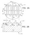
- FIG. 2Ais a top view of a semiconductor wafer 210 shown before the wafer is thinned with a dry etch.
- FIG. 2Bis a cross sectional view of the wafer along the lines II—II in FIG. 2 A.
- Circuitryhas been fabricated in the wafer, and the wafer must now be divided into chips 110 .
- the circuitrymay include transistors, diodes, and other devices (not shown) manufactured in and over an active layer 220 (FIG. 2B) adjacent to the wafer top surface 210 F (the surface shown in FIG. 2 A).
- Optional conductive bumps 216have been manufactured on contact pads on top surface 210 F of chips 110 . The bumps will be used to connect the chips to wiring substrates (not shown), e.g., printed circuit boards.
- the wafer thickness 240has been sufficiently large to achieve suitable mechanical strength and heat dissipation during fabrication of the wafer circuitry. 720 ⁇ m is suitable for some silicon wafer fabrication processes. The wafer will now to be thinned to its final thickness Hf. In some embodiments, the final thickness is 10-450 ⁇ m. These thickness figures are illustrative and not limiting.
- grooves 260were formed in the wafer top surface along scribe lines and, in particular, along the boundary of chips 110 .
- the groovescould be formed by conventional dicing techniques, e.g. with a diamond saw or a laser. Other processes, e.g., a masked etch, could also be used.
- the groovesdo not go through the wafer.
- the groovesare at least as deep as the final chip thickness Hf. In some embodiments, the groove depth is 10-450 ⁇ m.
- the grooveswill be exposed from the bottom during wafer thinning when the wafer back side 110 B is etched, as described below.
- the groove sidewall and bottom surfaces 270can be damaged by dicing, as schematically shown by uneven lines in FIGS. 2A, 2 B.
- Wafer 210is placed in a non-contact wafer holder 510 (FIG. 3 ).
- Holder 510includes one or more vortex chucks 520 having outlets in the holder's surface 524 .
- Surface 524faces the top surface of the wafer.
- Gas supplied under pressure through a conduit 522enter chucks 520 through respective passages 523 .
- Each passageis tangential to the chuck's cylindrical chamber when viewed from the top.
- a gas vortex 525 emitted by each chuck towards the wafergenerates a low pressure zone near the chuck's vertical axis. In this zone, the wafer is drawn towards the chuck. At the same time, the gas vortices do not allow the wafer to touch the holder surface 524 .
- Such wafer holdersare described, for example, in U.S. patent application Ser. No. 09/456,135 “Non-Contact Workpiece Holder” filed by O. Siniaguine et al. on Dec. 7, 1999 and incorporated herein by reference.
- Other suitable holdersare described in PCT publication WO 99/46805 (TruSi Technologies, LLC, Sep. 16, 1999) incorporated herein by reference.
- Other holdersfor example, Bernoulli type holders, electrostatic holders, mechanical clamps, or vacuum chucks, can also be used.
- Wafer holder 510is called “non-contact” because the top surface of the wafer does not contact the holder surface 524 . However, the edge of the wafer can contact the holder's limitors 526 which extend around the wafer to restrict the wafer lateral motion.
- holder 510is mounted on a rotating carousel (not shown). The carousel rotation develops a centrifugal force that presses the wafer against one or more limitors 526 . See PCT publication WO 99/26796 (TruSi Technologies, LLC, Jun. 3, 1999).
- the wafer backside surface 110 Bis etched with a dry etch.
- the etchis a blanket (unmasked) uniform etch of the wafer's flat semiconductor backside surface (e.g., silicon surface).
- the etchis atmospheric pressure plasma etch.
- Plasma generator 530generates plasma 540 into which suitable reagents are injected. If the wafer is made of silicon, a CF4 etch can be used. See PCT publication WO 98/19337 (TruSi Technologies, LLC, May 7, 1998) incorporated herein by reference.
- a suitable etcheris type Tru-Etch 3000 (trademark) available from TruSi Technologies, LLC, of Sunnyvale, Calif.
- the dry etchthins the wafer until the grooves 260 are exposed from the bottom.
- the plasmaenters the grooves and etches the groove sidewalls 270 .
- the sidewallsbecome smoother as a result.
- the dicing damagebecomes partially or completely removed from the sidewalls.
- the bottom corners and edges of chips 110become rounded.
- some atmospheric pressure plasma etching processes described in WO 98/19337are fast. Silicon can be etched at the rate of about 10 ⁇ m/min. Other kinds of etches can also be used. The dry etch can be preceded by mechanical lapping of the wafer bottom surface 110 B.
- the groove depth Hg(FIG. 2B) exceeds the final chip thickness by an amount needed to obtain the rounded edges and corners and smooth sidewalls for chips 110 .
- the more the groove depth exceeds the final chip thicknessthe longer the duration of the backside etch after the grooves have been exposed from the bottom.
- the bottom corners and edgesbecome more rounded, and more time is allowed for sidewall damage removal.
- the radius of the rounded cornersis roughly 1.5 times the thickness of the material removed from the wafer backside after the grooves are exposed.
- the depth of the groovesalso takes into account possible wafer non-uniformity, the non-uniformity of the dicing process that creates the grooves, and the non-uniformity of the backside etch. If mechanical lapping or any other process is used to remove material from the wafer backside before the dry etch illustrated in FIG. 5, the non-uniformity of such processes can also be taken into account.
- the groove depth Hgexceeds the final chip thickness Hf by 10 ⁇ m or more.
- each chip 110When the grooves 260 become exposed during the thinning etch of FIG. 3, chips 110 become separated from each other, but the chips are held in holder 510 by the vacuum forces developed by the gas vortices.
- the vortex chucks 520are positioned close to each other to insure that each chip 110 will be adjacent to a low pressure zone developed by at least one chuck 520 .
- Ldenotes the greatest lateral dimension of each chip 110 .
- Pis the distance between the centers of the adjacent chucks 520 .
- Dis the diameter of each chuck. “P” and “D” can vary for different chucks 520 in the same wafer holder.
- each vortex chuckshould be small enough to prevent a chip from being sucked into the chuck.
- the chipshould be balanced at a predetermined distance from the wafer holder surface 524 by the vacuum forces drawing the chip towards the holder and the opposite-direction forces generated between the chucks by the gas flowing away from the chucks. In some embodiments, D ⁇ L/2 and P ⁇ L/2 for all the chucks.
- each of P and Dis less than one half of the shortest side of each rectangular chip 110 .
- the distance between the adjacent chucks and the diameter of each chucktake into account the peripheral wafer portions 320 (FIG. 2 A).
- Each of P and Dis less than one half of the greatest lateral dimension, or of the longest or shortest side, of each portion 320 .
- FIG. 5is a perspective view of a chip 110 after the etch.
- the chipis shown bottom side up.
- the chip's sidewalls 110 S and bottom surface 110 Bare smooth.
- the edges 110 E at which the sidewalls 110 S meet with each other and with the bottom surface 110 Bare rounded, and so are the bottom corners 110 C.
- the smooth surfaces and the rounded edges and cornersprolong the chip's lifetime and improve the chip's reliability.
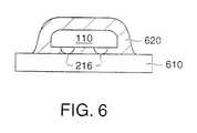
- chip 110has been mounted on a printed circuit board 610 using flip chip technology.
- Bumps 216are soldered to the printed circuit board.
- Encapsulant 620(suitable plastic) is deposited over the chip for protective purposes. The chip's smooth surfaces and rounded edges and corners prolong the chip's lifetime. Similar advantages are achieved with non-flip-chip packaging.
- the etch uniformityis improved by depositing a layer 310 over grooves 260 and wafer portions adjacent to the grooves.
- Layer 310is deposited before the backside etch of the wafer.
- the layer 310holds the chips and the portions 320 in the same position relative to each other. Therefore, the gaps between the chips 110 and the peripheral portions 320 remain uniform, and hence the chip sidewalls (the sidewalls of grooves 260 ) are etched uniformly. If some chips 110 were too close to each other or to peripheral portions 320 , the chips' sidewalls could be etched too slowly, and less damage would be removed than desirable. Other sidewalls, farther from adjacent chips 110 or portions 320 , could be undesirably overetched.
- Layer 310also relaxes the requirements for the distance between adjacent vortex chucks 520 and the diameter of each chuck since the chips 110 and peripheral portions 320 are held in position by layer 310 throughout the backside etch.
- Layer 310can be a sticky material which adheres to the wafer without additional adhesive. Alternatively, adhesives can be used.
- layer 310is polyimide. Polyimide is chosen because it does not react with etchants utilized in some thinning processes (e.g., CF4). The thickness of polyimide layer 310 is 1 ⁇ m to 200 ⁇ m in some embodiments. Other materials and thicknesses can also be used.
- layer 310is an adhesive tape such as described in U.S. Pat. No. 5,888,883 issued on Mar. 30, 1999 to Sasaki et al.
- Layer 310does not cover the middle portions of chips 110 , including the bumps 216 .
- the bumps, and any other uneven features of the chip top surface 210 F,are believed to be capable of impeding adhesion of layer 310 to the wafer.
- layer 310is pre-manufactured as a continuous sheet. Then openings are cut out in layer 310 at the location of the middle portions of chips 110 . Then layer 310 is deposited.
- Layer 310can be deposited using known techniques. In some embodiments, layer 310 is deposited at atmospheric pressure using a roller to remove air bubbles. Alternatively, layer 310 can be laminated on the wafer in vacuum, with or without a roller.
- layer 310covers peripheral portions 320 . In FIG. 8, layer 310 covers the entire wafer. In some embodiments, the top surface of chips 110 is even, bumps 216 are absent.
- the inventionis not limited to layer 310 covering or exposing any particular features of the wafer.
- Layer 310prevents the plasma from going through the grooves 260 and damaging the circuitry at the top surface of the wafer.
- Gas emitted by chucks 520flows down around the wafer as shown at 550 in FIG. 3, and impedes the plasma from flowing up around the wafer and reaching the wafer top surface.
- the chuck densitycan be made high at the edge of wafer holder 510 to prevent the plasma from flowing up around the wafer.
- Gascan be made to flow down at all points around the wafer.
- layer 310has been deposited by a spin-on or spraying technique. Layer 310 fills grooves 260 . (In contrast, in FIGS. 7 and 8, the grooves are not filled.) Layer 310 in FIG. 9 can be polymer or some other material.
- FIG. 10shows the structure after the backside etch for FIG. 9 .
- layer 310when layer 310 is exposed from the bottom, layer 310 is etched faster than the wafer substrate. Therefore, the bottom surface of layer 310 is higher than the bottom surface of chips 110 and peripheral portions 320 . The bottom corners and edges of chips 110 have been exposed to the etchant, and have been rounded.
- FIG. 11illustrates an embodiment in which the layer 310 is etched slower than the wafer substrate. This is the case if layer 310 is polyimide, the wafer is a silicon wafer, and the etch is a CF4 plasma etch. Layer 310 is etched slowly, but the microloading effect causes the chips 110 to be etched faster at the bottom edges adjacent to layer 310 . As a result, the bottom edges and corners of chips 110 are rounded.
- layer 310is removed.
- polyimide layer 310is removed by oxygen plasma.
- the sidewall etch rateis reduced while the vertical etch rate at the bottom of the wafer remains the same.
- a high vertical etch rateis desirable because it reduces the dicing time and also reduces the time needed to remove jagged edges protruding from the grooves' sidewalls.
- the aspect ratio A 1is chosen to be at least 0.5, or at least 1, or at least 1.2, or at least 2, or at least 3, or at least 4, or at least 5, or at least some other number.
- the waferis diced with a saw, and the groove width Wg is 25 to 30 ⁇ m (depending on the saw).
- the waferis diced with a laser apparatus, and the groove width Wg is about 100 ⁇ m.
- the waferis diced with a dry etch (for example, RIE), and the groove width is 5 ⁇ m.
- the groove width Wgis measured at the top of the wafer. (If the wafer is diced with a dry etch, the groove sidewalls are not necessarily vertical, and the groove width may vary with depth.)
- the waferis diced while being attached to tape 310 (FIGS. 7, 8 ).
- the final wafer thickness Hfis 100 ⁇ m
- the groove depth Hgis slightly higher, for example, 110 ⁇ m.
- Hgcan be 30 ⁇ m or some other value.
- a 2represents the aspect ratio at the end of the backside etch.
- Appropriate bound values for A 2 , A 3 , A 4include 0.5, 1, 1.2, 2, 3, 4, 5, or other values.
- the inventionis not limited by any particular mathematical formula for defining a lower bound for A 1 , A 2 , A 3 , or A 4 .
- defining a lower bound for Hf/Wfhas the same effect as defining an upper bound for Wf/Hf.
- Hg ⁇ Hfso if Hg/Wg ⁇ LB (some lower bound), then Hf/Wg ⁇ LB.
- Other mathematical dependenciescan also be explored to define a limitation on the horizontal etch rate of the grooves' sidewalls.
- the inventionis not limited to isotropic backside etches.
- an anisotropic etchis used, e.g., vacuum plasma RIE (reactive ion etching).
- the etchant's ionsare reflected from tape 310 which is made, for example, from an organic compound resistant to the echant. These reflected ions hit the grooves' sidewalls, so the sidewalls are etched horizontally. A high aspect ratio of the grooves retards horizontal etching.
- each of the parameters Hg, Wg, Hf, Wfhas the same value throughout the wafer, but the invention is not limited to such embodiments.
- different groovesmay have different widths Wg in the same wafer.
- the grooves between adjacent chips 110have the same depth and width as the grooves separating the chips 110 from the peripheral portions 320 , but this is not necessary.
- the above embodimentsillustrate but do not limit the invention.
- the inventionis not limited to silicon wafers or any packaging technology.
- the inventionis not limited to plasma etching, or to any particular etch chemistry or type of etcher.
- the lateral etch rate at the groove sidewallsis reduced by a suitable choice of etching parameters.
- the waferin a vacuum plasma etch, can be held at a suitable potential to steer ions vertically towards the wafer and not laterally. Such potential may be tens or hundreds of volts, for example.
- the inventionis not limited to wafers containing multiple chips. In some embodiments, only one chip has been fabricated in the wafer. The chip is extracted and the wafer peripheral portions 320 are discarded.
- the inventionis not limited to unmasked or uniform backside etches. Other embodiments and variations are within the scope of the invention, as defined by the appended claims.
Landscapes
- Engineering & Computer Science (AREA)
- Microelectronics & Electronic Packaging (AREA)
- Power Engineering (AREA)
- Computer Hardware Design (AREA)
- Physics & Mathematics (AREA)
- Condensed Matter Physics & Semiconductors (AREA)
- General Physics & Mathematics (AREA)
- Manufacturing & Machinery (AREA)
- Dicing (AREA)
- Drying Of Semiconductors (AREA)
Abstract
Description
Claims (17)
Priority Applications (1)
| Application Number | Priority Date | Filing Date | Title |
|---|---|---|---|
| US09/876,888US6498074B2 (en) | 1996-10-29 | 2001-06-06 | Thinning and dicing of semiconductor wafers using dry etch, and obtaining semiconductor chips with rounded bottom edges and corners |
Applications Claiming Priority (6)
| Application Number | Priority Date | Filing Date | Title |
|---|---|---|---|
| US3042596P | 1996-10-29 | 1996-10-29 | |
| PCT/US1997/018979WO1998019337A1 (en) | 1996-10-29 | 1997-10-27 | Integrated circuits and methods for their fabrication |
| US09/083,927US6184060B1 (en) | 1996-10-29 | 1998-05-22 | Integrated circuits and methods for their fabrication |
| US49145600A | 2000-01-26 | 2000-01-26 | |
| US09/752,802US6448153B2 (en) | 1996-10-29 | 2000-12-28 | Thinning and dicing of semiconductor wafers using dry etch, and obtaining semiconductor chips with rounded bottom edges and corners |
| US09/876,888US6498074B2 (en) | 1996-10-29 | 2001-06-06 | Thinning and dicing of semiconductor wafers using dry etch, and obtaining semiconductor chips with rounded bottom edges and corners |
Related Parent Applications (1)
| Application Number | Title | Priority Date | Filing Date |
|---|---|---|---|
| US09/752,802Continuation-In-PartUS6448153B2 (en) | 1996-10-29 | 2000-12-28 | Thinning and dicing of semiconductor wafers using dry etch, and obtaining semiconductor chips with rounded bottom edges and corners |
Publications (2)
| Publication Number | Publication Date |
|---|---|
| US20020013061A1 US20020013061A1 (en) | 2002-01-31 |
| US6498074B2true US6498074B2 (en) | 2002-12-24 |
Family
ID=27487812
Family Applications (1)
| Application Number | Title | Priority Date | Filing Date |
|---|---|---|---|
| US09/876,888Expired - LifetimeUS6498074B2 (en) | 1996-10-29 | 2001-06-06 | Thinning and dicing of semiconductor wafers using dry etch, and obtaining semiconductor chips with rounded bottom edges and corners |
Country Status (1)
| Country | Link |
|---|---|
| US (1) | US6498074B2 (en) |
Cited By (38)
| Publication number | Priority date | Publication date | Assignee | Title |
|---|---|---|---|---|
| US20040142574A1 (en)* | 2002-03-19 | 2004-07-22 | Seiko Epson Corporation | Semiconductor device and method of manufacturing the same, circuit board, and electronic instrument |
| US6869831B2 (en)* | 2001-09-14 | 2005-03-22 | Texas Instruments Incorporated | Adhesion by plasma conditioning of semiconductor chip surfaces |
| US20050064683A1 (en)* | 2003-09-19 | 2005-03-24 | Farnworth Warren M. | Method and apparatus for supporting wafers for die singulation and subsequent handling |
| US20050064681A1 (en)* | 2003-09-19 | 2005-03-24 | Wood Alan G. | Support structure for thinning semiconductor substrates and thinning methods employing the support structure |
| US20050064679A1 (en)* | 2003-09-19 | 2005-03-24 | Farnworth Warren M. | Consolidatable composite materials, articles of manufacture formed therefrom, and fabrication methods |
| US20050133930A1 (en)* | 2003-12-17 | 2005-06-23 | Sergey Savastisuk | Packaging substrates for integrated circuits and soldering methods |
| US20050136634A1 (en)* | 2003-12-17 | 2005-06-23 | Sergey Savastiouk | Integrated circuits and packaging substrates with cavities, and attachment methods including insertion of protruding contact pads into cavities |
| US6924210B1 (en) | 2004-03-06 | 2005-08-02 | International Business Machines Corporation | Chip dicing |
| US20050200004A1 (en)* | 2002-09-02 | 2005-09-15 | Naoyuki Koizumi | Semiconductor chip and fabrication method thereof |
| US20050245005A1 (en)* | 2004-04-29 | 2005-11-03 | Benson Peter A | Wafer edge ring structures and methods of formation |
| US20060040467A1 (en)* | 2004-08-20 | 2006-02-23 | Dolechek Kert L | Process and apparatus for thinning a semiconductor workpiece |
| US20060040111A1 (en)* | 2004-08-20 | 2006-02-23 | Dolechek Kert L | Process chamber and system for thinning a semiconductor workpiece |
| US20060046499A1 (en)* | 2004-08-20 | 2006-03-02 | Dolechek Kert L | Apparatus for use in thinning a semiconductor workpiece |
| WO2006048230A1 (en) | 2004-11-01 | 2006-05-11 | Xsil Technology Limited | Increasing die strength by etching during or after dicing |
| US20060118515A1 (en)* | 2004-08-20 | 2006-06-08 | Semitool, Inc. | Process For Thinning A Semiconductor Workpiece |
| US20070001321A1 (en)* | 2004-06-14 | 2007-01-04 | Hembree David R | Semiconductor devices at least partially covered by a composite coating including particles dispersed through photopolymer material |
| US20070173032A1 (en)* | 2006-01-25 | 2007-07-26 | Lexmark International, Inc. | Wafer dicing by channels and saw |
| US20070187802A1 (en)* | 2003-05-16 | 2007-08-16 | Kabushiki Kaisha Toshiba | Semiconductor device and manufacturing method thereof |
| US20070262420A1 (en)* | 2005-01-24 | 2007-11-15 | Kiyoshi Arita | Manufacturing Method for Semiconductor Chips, and Semiconductor Chip |
| CN100355036C (en)* | 2003-02-25 | 2007-12-12 | 三洋电机株式会社 | Manufacturing method of semiconductor device |
| US7354649B2 (en) | 2004-08-20 | 2008-04-08 | Semitool, Inc. | Semiconductor workpiece |
| US7442643B2 (en) | 2004-09-02 | 2008-10-28 | Micron Technology, Inc. | Methods of forming conductive elements using organometallic layers and flowable, curable conductive materials |
| US20090068798A1 (en)* | 2007-09-07 | 2009-03-12 | Micron Technology, Inc. | Imager die package and methods of packaging an imager die on a temporary carrier |
| US20090085232A1 (en)* | 2007-09-28 | 2009-04-02 | Ong King Hoo | Method of reducing memory card edge roughness by edge coating |
| US20090137097A1 (en)* | 2007-11-26 | 2009-05-28 | United Microelectronics Corp. | Method for dicing wafer |
| GB2459301A (en)* | 2008-04-18 | 2009-10-21 | Xsil Technology Ltd | A method of dicing wafers to give high die strength |
| GB2459302A (en)* | 2008-04-18 | 2009-10-21 | Xsil Technology Ltd | A method of dicing wafers to give high die strength |
| US20100140753A1 (en)* | 2005-04-08 | 2010-06-10 | Hembree David R | Stacked Semiconductor Component Having Through Wire Interconnect And Method Of Fabrication |
| US7768096B2 (en)* | 2005-05-19 | 2010-08-03 | Micron Technology, Inc. | System for fabricating semiconductor components with conductive interconnects |
| US7786605B2 (en) | 2005-12-07 | 2010-08-31 | Micron Technology, Inc. | Stacked semiconductor components with through wire interconnects (TWI) |
| US20100311223A1 (en)* | 2009-06-05 | 2010-12-09 | Chun Jung Hwan | Method Of Dicing Wafer Using Plasma |
| US20110062564A1 (en)* | 2009-09-17 | 2011-03-17 | Gruenhagen Michael D | Semiconductor die containing lateral edge shapes and textures |
| US20110221053A1 (en)* | 2010-03-11 | 2011-09-15 | Qualcomm Incorporated | Pre-processing to reduce wafer level warpage |
| US8120167B2 (en) | 2006-04-24 | 2012-02-21 | Micron Technology, Inc. | System with semiconductor components having encapsulated through wire interconnects (TWI) |
| US8623703B2 (en) | 2011-01-13 | 2014-01-07 | Seiko Epson Corporation | Silicon device and silicon device manufacturing method |
| US20140213042A1 (en)* | 2013-01-25 | 2014-07-31 | Wei-Sheng Lei | Substrate dicing by laser ablation & plasma etch damage removal for ultra-thin wafers |
| US10211175B2 (en) | 2012-11-30 | 2019-02-19 | International Business Machines Corporation | Stress-resilient chip structure and dicing process |
| US11990484B2 (en) | 2018-01-30 | 2024-05-21 | Pragmatic Printing Ltd. | Integrated circuit on flexible substrate manufacturing process |
Families Citing this family (26)
| Publication number | Priority date | Publication date | Assignee | Title |
|---|---|---|---|---|
| US6869870B2 (en)* | 1998-12-21 | 2005-03-22 | Megic Corporation | High performance system-on-chip discrete components using post passivation process |
| DE19962431B4 (en)* | 1999-12-22 | 2005-10-20 | Micronas Gmbh | Method for producing a semiconductor system with adhesive zone for a passivation layer |
| KR101037142B1 (en) | 2002-04-19 | 2011-05-26 | 일렉트로 사이언티픽 인더스트리즈, 아이엔씨 | Program-controlled dicing of substrate using pulse laser |
| US6743699B1 (en)* | 2003-01-21 | 2004-06-01 | Micron Technology, Inc. | Method of fabricating semiconductor components |
| US7507638B2 (en)* | 2004-06-30 | 2009-03-24 | Freescale Semiconductor, Inc. | Ultra-thin die and method of fabricating same |
| WO2006043122A1 (en)* | 2004-10-21 | 2006-04-27 | Infineon Technologies Ag | Semiconductor package and method to produce the same |
| US7635418B2 (en)* | 2004-12-03 | 2009-12-22 | Nordson Corporation | Plasma processing apparatus and methods for removing extraneous material from selected areas on a substrate |
| JP4731191B2 (en)* | 2005-03-28 | 2011-07-20 | 富士通セミコンダクター株式会社 | Semiconductor device and manufacturing method of semiconductor device |
| JP4544143B2 (en)* | 2005-06-17 | 2010-09-15 | セイコーエプソン株式会社 | Semiconductor device manufacturing method, semiconductor device, circuit board, and electronic apparatus |
| KR100863333B1 (en) | 2007-06-27 | 2008-10-15 | 주식회사 효광 | Substrate processing method and chips manufactured thereby |
| JP2010103300A (en)* | 2008-10-23 | 2010-05-06 | Sanyo Electric Co Ltd | Semiconductor device, and method of manufacturing the same |
| US8168470B2 (en) | 2008-12-08 | 2012-05-01 | Stats Chippac, Ltd. | Semiconductor device and method of forming vertical interconnect structure in substrate for IPD and baseband circuit separated by high-resistivity molding compound |
| US8609512B2 (en)* | 2009-03-27 | 2013-12-17 | Electro Scientific Industries, Inc. | Method for laser singulation of chip scale packages on glass substrates |
| US8298917B2 (en)* | 2009-04-14 | 2012-10-30 | International Business Machines Corporation | Process for wet singulation using a dicing singulation structure |
| EP2430652B1 (en) | 2009-05-12 | 2019-11-20 | The Board of Trustees of the University of Illionis | Printed assemblies of ultrathin, microscale inorganic light emitting diodes for deformable and semitransparent displays |
| US8168474B1 (en) | 2011-01-10 | 2012-05-01 | International Business Machines Corporation | Self-dicing chips using through silicon vias |
| US9765934B2 (en) | 2011-05-16 | 2017-09-19 | The Board Of Trustees Of The University Of Illinois | Thermally managed LED arrays assembled by printing |
| US9099547B2 (en)* | 2011-10-04 | 2015-08-04 | Infineon Technologies Ag | Testing process for semiconductor devices |
| US9455192B2 (en) | 2014-03-26 | 2016-09-27 | Infineon Technologies Ag | Kerf preparation for backside metallization |
| US9397055B2 (en) | 2014-05-29 | 2016-07-19 | Infineon Technologies Ag | Processing of thick metal pads |
| US9601437B2 (en)* | 2014-09-09 | 2017-03-21 | Nxp B.V. | Plasma etching and stealth dicing laser process |
| EP3171399B1 (en)* | 2015-11-18 | 2020-06-03 | IMEC vzw | Method for singulating a stack of semiconductor wafers |
| DE102017104859A1 (en) | 2017-03-08 | 2018-09-13 | Osram Opto Semiconductors Gmbh | Semiconductor component and method for producing at least one semiconductor component |
| US11402579B2 (en) | 2017-12-27 | 2022-08-02 | Medlumics S.L. | Techniques for fabricating waveguide facets and die separation |
| TWI771893B (en)* | 2021-02-03 | 2022-07-21 | 國立陽明交通大學 | Method for cutting an array of chips |
| KR20230025597A (en) | 2021-08-13 | 2023-02-22 | 삼성전자주식회사 | Semiconductor package and method of forming the same |
Citations (79)
| Publication number | Priority date | Publication date | Assignee | Title |
|---|---|---|---|---|
| US3739463A (en) | 1971-10-18 | 1973-06-19 | Gen Electric | Method for lead attachment to pellets mounted in wafer alignment |
| US3761782A (en) | 1971-05-19 | 1973-09-25 | Signetics Corp | Semiconductor structure, assembly and method |
| US3810129A (en) | 1972-10-19 | 1974-05-07 | Ibm | Memory system restoration |
| US3838501A (en) | 1973-02-09 | 1974-10-01 | Honeywell Inf Systems | Method in microcircuit package assembly providing nonabrasive, electrically passive edges on integrated circuit chips |
| US3881884A (en) | 1973-10-12 | 1975-05-06 | Ibm | Method for the formation of corrosion resistant electronic interconnections |
| US3991296A (en) | 1974-11-15 | 1976-11-09 | Nippon Electric Company, Ltd. | Apparatus for forming grooves on a wafer by use of a laser |
| US3993917A (en) | 1975-05-29 | 1976-11-23 | International Business Machines Corporation | Parameter independent FET sense amplifier |
| US4139401A (en) | 1963-12-04 | 1979-02-13 | Rockwell International Corporation | Method of producing electrically isolated semiconductor devices on common crystalline substrate |
| US4141135A (en) | 1975-10-14 | 1979-02-27 | Thomson-Csf | Semiconductor process using lapped substrate and lapped low resistivity semiconductor carrier |
| US4368106A (en) | 1980-10-27 | 1983-01-11 | General Electric Company | Implantation of electrical feed-through conductors |
| US4394712A (en) | 1981-03-18 | 1983-07-19 | General Electric Company | Alignment-enhancing feed-through conductors for stackable silicon-on-sapphire wafers |
| US4463336A (en) | 1981-12-28 | 1984-07-31 | United Technologies Corporation | Ultra-thin microelectronic pressure sensors |
| US4467518A (en) | 1981-05-19 | 1984-08-28 | Ibm Corporation | Process for fabrication of stacked, complementary MOS field effect transistor circuits |
| US4603341A (en) | 1983-09-08 | 1986-07-29 | International Business Machines Corporation | Stacked double dense read only memory |
| US4612083A (en) | 1984-07-20 | 1986-09-16 | Nec Corporation | Process of fabricating three-dimensional semiconductor device |
| US4628174A (en) | 1984-09-17 | 1986-12-09 | General Electric Company | Forming electrical conductors in long microdiameter holes |
| US4722130A (en) | 1984-11-07 | 1988-02-02 | Kabushiki Kaisha Toshiba | Method of manufacturing a semiconductor device |
| US4729971A (en) | 1987-03-31 | 1988-03-08 | Microwave Semiconductor Corporation | Semiconductor wafer dicing techniques |
| US4769738A (en) | 1986-12-12 | 1988-09-06 | Fuji Electric Co., Ltd. | Electrostatic capacitive pressure sensor |
| US4807021A (en) | 1986-03-10 | 1989-02-21 | Kabushiki Kaisha Toshiba | Semiconductor device having stacking structure |
| US4822755A (en) | 1988-04-25 | 1989-04-18 | Xerox Corporation | Method of fabricating large area semiconductor arrays |
| US4842699A (en) | 1988-05-10 | 1989-06-27 | Avantek, Inc. | Method of selective via-hole and heat sink plating using a metal mask |
| US4897708A (en) | 1986-07-17 | 1990-01-30 | Laser Dynamics, Inc. | Semiconductor wafer array |
| US4978639A (en) | 1989-01-10 | 1990-12-18 | Avantek, Inc. | Method for the simultaneous formation of via-holes and wraparound plating on semiconductor chips |
| US4996587A (en) | 1989-04-10 | 1991-02-26 | International Business Machines Corporation | Integrated semiconductor chip package |
| US5024970A (en) | 1989-06-27 | 1991-06-18 | Mitsubishi Denki Kabushiki Kaisha | Method of obtaining semiconductor chips |
| WO1992003848A2 (en) | 1990-08-28 | 1992-03-05 | Lsi Logic Europe Plc | Stacking of integrated circuits |
| US5160987A (en) | 1989-10-26 | 1992-11-03 | International Business Machines Corporation | Three-dimensional semiconductor structures formed from planar layers |
| US5191405A (en) | 1988-12-23 | 1993-03-02 | Matsushita Electric Industrial Co., Ltd. | Three-dimensional stacked lsi |
| US5229647A (en) | 1991-03-27 | 1993-07-20 | Micron Technology, Inc. | High density data storage using stacked wafers |
| US5259924A (en) | 1992-04-08 | 1993-11-09 | Micron Technology, Inc. | Integrated circuit fabrication process to reduce critical dimension loss during etching |
| US5268326A (en) | 1992-09-28 | 1993-12-07 | Motorola, Inc. | Method of making dielectric and conductive isolated island |
| US5270261A (en) | 1991-09-13 | 1993-12-14 | International Business Machines Corporation | Three dimensional multichip package methods of fabrication |
| WO1994009513A1 (en) | 1992-10-13 | 1994-04-28 | Glenn Leedy | Interconnection structure for integrated circuits and method for making same |
| US5307942A (en) | 1991-11-29 | 1994-05-03 | Alcatel Cit | Electronic, especially telecommunication equipment rack |
| US5309318A (en) | 1992-04-21 | 1994-05-03 | International Business Machines Corporation | Thermally enhanced semiconductor chip package |
| US5313097A (en) | 1992-11-16 | 1994-05-17 | International Business Machines, Corp. | High density memory module |
| US5314844A (en) | 1991-03-04 | 1994-05-24 | Kabushiki Kaisha Toshiba | Method for dicing a semiconductor wafer |
| WO1994025981A1 (en) | 1993-05-05 | 1994-11-10 | Siemens Aktiengesellschaft | Process for producing vertically connected semiconductor components |
| US5414637A (en) | 1992-06-24 | 1995-05-09 | International Business Machines Corporation | Intra-module spare routing for high density electronic packages |
| US5426566A (en) | 1991-09-30 | 1995-06-20 | International Business Machines Corporation | Multichip integrated circuit packages and systems |
| US5466634A (en) | 1994-12-20 | 1995-11-14 | International Business Machines Corporation | Electronic modules with interconnected surface metallization layers and fabrication methods therefore |
| US5467305A (en) | 1992-03-12 | 1995-11-14 | International Business Machines Corporation | Three-dimensional direct-write EEPROM arrays and fabrication methods |
| US5478781A (en) | 1993-06-21 | 1995-12-26 | International Business Machines Corporation | Polyimide-insulated cube package of stacked semiconductor device chips |
| US5502333A (en) | 1994-03-30 | 1996-03-26 | International Business Machines Corporation | Semiconductor stack structures and fabrication/sparing methods utilizing programmable spare circuit |
| US5502667A (en) | 1993-09-13 | 1996-03-26 | International Business Machines Corporation | Integrated multichip memory module structure |
| US5506753A (en) | 1994-09-26 | 1996-04-09 | International Business Machines Corporation | Method and apparatus for a stress relieved electronic module |
| US5517754A (en) | 1994-06-02 | 1996-05-21 | International Business Machines Corporation | Fabrication processes for monolithic electronic modules |
| US5532519A (en) | 1994-09-14 | 1996-07-02 | International Business Machines Corporation | Cube wireability enhancement with chip-to-chip alignment and thickness control |
| WO1996021943A1 (en) | 1995-01-13 | 1996-07-18 | ZAKRYTOE AKTSIONERNOE OBSCHESTVO PROIZVODSTVENNAYA FIRMA 'Az' | Device for treating planar elements with a plasma jet |
| US5561622A (en) | 1993-09-13 | 1996-10-01 | International Business Machines Corporation | Integrated memory cube structure |
| US5567654A (en) | 1994-09-28 | 1996-10-22 | International Business Machines Corporation | Method and workpiece for connecting a thin layer to a monolithic electronic module's surface and associated module packaging |
| US5571754A (en) | 1995-07-26 | 1996-11-05 | International Business Machines Corporation | Method of fabrication of endcap chip with conductive, monolithic L-connect for multichip stack |
| US5596226A (en) | 1994-09-06 | 1997-01-21 | International Business Machines Corporation | Semiconductor chip having a chip metal layer and a transfer metal and corresponding electronic module |
| EP0757431A2 (en) | 1995-08-03 | 1997-02-05 | International Business Machines Corporation | Machine structures fabricated of multiple microstructure layers |
| US5646067A (en) | 1995-06-05 | 1997-07-08 | Harris Corporation | Method of bonding wafers having vias including conductive material |
| US5656553A (en) | 1994-08-22 | 1997-08-12 | International Business Machines Corporation | Method for forming a monolithic electronic module by dicing wafer stacks |
| US5691248A (en) | 1995-07-26 | 1997-11-25 | International Business Machines Corporation | Methods for precise definition of integrated circuit chip edges |
| WO1997045856A1 (en) | 1996-05-31 | 1997-12-04 | Ipec Precision, Inc. | Method for treating articles with a plasma jet |
| WO1997045862A1 (en) | 1996-05-31 | 1997-12-04 | Ipec Precision, Inc. | Non-contact holder for wafer-like articles |
| US5707485A (en) | 1995-12-20 | 1998-01-13 | Micron Technology, Inc. | Method and apparatus for facilitating removal of material from the backside of wafers via a plasma etch |
| DE19707887A1 (en) | 1997-02-27 | 1998-09-10 | Micronas Semiconductor Holding | Process for the production of electronic elements |
| US5824595A (en) | 1995-10-17 | 1998-10-20 | Deutsche Itt Industries Gmbh | Method of separating electronic elements |
| US5843844A (en) | 1995-01-25 | 1998-12-01 | Matsushita Electric Industrial Co., Ltd. | Probe sheet and method of manufacturing the same |
| US5846879A (en) | 1993-05-05 | 1998-12-08 | Siemens Aktiengesellschaft | Contact structure for vertical chip connections |
| US5851845A (en) | 1995-12-18 | 1998-12-22 | Micron Technology, Inc. | Process for packaging a semiconductor die using dicing and testing |
| US5858256A (en)* | 1996-07-11 | 1999-01-12 | The Board Of Trustees Of The Leland Stanford, Jr. University | Method of forming small aperture |
| US5888883A (en) | 1997-07-23 | 1999-03-30 | Kabushiki Kaisha Toshiba | Method of dividing a wafer and method of manufacturing a semiconductor device |
| US5888882A (en) | 1996-04-04 | 1999-03-30 | Deutsche Itt Industries Gmbh | Process for separating electronic devices |
| US5979475A (en) | 1994-04-28 | 1999-11-09 | Hitachi, Ltd. | Specimen holding method and fluid treatment method of specimen surface and systems therefor |
| US5998292A (en) | 1997-11-12 | 1999-12-07 | International Business Machines Corporation | Method for making three dimensional circuit integration |
| US6004867A (en) | 1996-12-16 | 1999-12-21 | Samsung Electronics Co., Ltd. | Chip-size packages assembled using mass production techniques at the wafer-level |
| US6036872A (en)* | 1998-03-31 | 2000-03-14 | Honeywell Inc. | Method for making a wafer-pair having sealed chambers |
| US6083811A (en) | 1996-02-07 | 2000-07-04 | Northrop Grumman Corporation | Method for producing thin dice from fragile materials |
| US6121119A (en) | 1994-06-09 | 2000-09-19 | Chipscale, Inc. | Resistor fabrication |
| US6162701A (en) | 1995-05-18 | 2000-12-19 | Hitachi, Ltd. | Semiconductor device and method for making same |
| US6176966B1 (en) | 1997-06-12 | 2001-01-23 | Lintec Corporation | Method of die bonding electronic component and die bonding apparatus thereof |
| US6184060B1 (en) | 1996-10-29 | 2001-02-06 | Trusi Technologies Llc | Integrated circuits and methods for their fabrication |
| US9752802B2 (en)* | 2013-12-16 | 2017-09-05 | Sumitomo Heavy Industries, Ltd. | Regenerative refrigerator |
- 2001
- 2001-06-06USUS09/876,888patent/US6498074B2/ennot_activeExpired - Lifetime
Patent Citations (86)
| Publication number | Priority date | Publication date | Assignee | Title |
|---|---|---|---|---|
| US4139401A (en) | 1963-12-04 | 1979-02-13 | Rockwell International Corporation | Method of producing electrically isolated semiconductor devices on common crystalline substrate |
| US3761782A (en) | 1971-05-19 | 1973-09-25 | Signetics Corp | Semiconductor structure, assembly and method |
| US3739463A (en) | 1971-10-18 | 1973-06-19 | Gen Electric | Method for lead attachment to pellets mounted in wafer alignment |
| US3810129A (en) | 1972-10-19 | 1974-05-07 | Ibm | Memory system restoration |
| US3811117A (en) | 1972-10-19 | 1974-05-14 | Ibm | Time ordered memory system and operation |
| US3838501A (en) | 1973-02-09 | 1974-10-01 | Honeywell Inf Systems | Method in microcircuit package assembly providing nonabrasive, electrically passive edges on integrated circuit chips |
| US3881884A (en) | 1973-10-12 | 1975-05-06 | Ibm | Method for the formation of corrosion resistant electronic interconnections |
| US3991296A (en) | 1974-11-15 | 1976-11-09 | Nippon Electric Company, Ltd. | Apparatus for forming grooves on a wafer by use of a laser |
| US3993917A (en) | 1975-05-29 | 1976-11-23 | International Business Machines Corporation | Parameter independent FET sense amplifier |
| US4141135A (en) | 1975-10-14 | 1979-02-27 | Thomson-Csf | Semiconductor process using lapped substrate and lapped low resistivity semiconductor carrier |
| US4368106A (en) | 1980-10-27 | 1983-01-11 | General Electric Company | Implantation of electrical feed-through conductors |
| US4394712A (en) | 1981-03-18 | 1983-07-19 | General Electric Company | Alignment-enhancing feed-through conductors for stackable silicon-on-sapphire wafers |
| US4467518A (en) | 1981-05-19 | 1984-08-28 | Ibm Corporation | Process for fabrication of stacked, complementary MOS field effect transistor circuits |
| US4463336A (en) | 1981-12-28 | 1984-07-31 | United Technologies Corporation | Ultra-thin microelectronic pressure sensors |
| US4603341A (en) | 1983-09-08 | 1986-07-29 | International Business Machines Corporation | Stacked double dense read only memory |
| US4612083A (en) | 1984-07-20 | 1986-09-16 | Nec Corporation | Process of fabricating three-dimensional semiconductor device |
| US4628174A (en) | 1984-09-17 | 1986-12-09 | General Electric Company | Forming electrical conductors in long microdiameter holes |
| US4722130A (en) | 1984-11-07 | 1988-02-02 | Kabushiki Kaisha Toshiba | Method of manufacturing a semiconductor device |
| US4807021A (en) | 1986-03-10 | 1989-02-21 | Kabushiki Kaisha Toshiba | Semiconductor device having stacking structure |
| US4897708A (en) | 1986-07-17 | 1990-01-30 | Laser Dynamics, Inc. | Semiconductor wafer array |
| US4769738A (en) | 1986-12-12 | 1988-09-06 | Fuji Electric Co., Ltd. | Electrostatic capacitive pressure sensor |
| US4729971A (en) | 1987-03-31 | 1988-03-08 | Microwave Semiconductor Corporation | Semiconductor wafer dicing techniques |
| US4822755A (en) | 1988-04-25 | 1989-04-18 | Xerox Corporation | Method of fabricating large area semiconductor arrays |
| US4842699A (en) | 1988-05-10 | 1989-06-27 | Avantek, Inc. | Method of selective via-hole and heat sink plating using a metal mask |
| US5191405A (en) | 1988-12-23 | 1993-03-02 | Matsushita Electric Industrial Co., Ltd. | Three-dimensional stacked lsi |
| US4978639A (en) | 1989-01-10 | 1990-12-18 | Avantek, Inc. | Method for the simultaneous formation of via-holes and wraparound plating on semiconductor chips |
| US4996587A (en) | 1989-04-10 | 1991-02-26 | International Business Machines Corporation | Integrated semiconductor chip package |
| US5024970A (en) | 1989-06-27 | 1991-06-18 | Mitsubishi Denki Kabushiki Kaisha | Method of obtaining semiconductor chips |
| US5160987A (en) | 1989-10-26 | 1992-11-03 | International Business Machines Corporation | Three-dimensional semiconductor structures formed from planar layers |
| WO1992003848A2 (en) | 1990-08-28 | 1992-03-05 | Lsi Logic Europe Plc | Stacking of integrated circuits |
| US5314844A (en) | 1991-03-04 | 1994-05-24 | Kabushiki Kaisha Toshiba | Method for dicing a semiconductor wafer |
| US5229647A (en) | 1991-03-27 | 1993-07-20 | Micron Technology, Inc. | High density data storage using stacked wafers |
| US5270261A (en) | 1991-09-13 | 1993-12-14 | International Business Machines Corporation | Three dimensional multichip package methods of fabrication |
| US5426566A (en) | 1991-09-30 | 1995-06-20 | International Business Machines Corporation | Multichip integrated circuit packages and systems |
| US5307942A (en) | 1991-11-29 | 1994-05-03 | Alcatel Cit | Electronic, especially telecommunication equipment rack |
| US5467305A (en) | 1992-03-12 | 1995-11-14 | International Business Machines Corporation | Three-dimensional direct-write EEPROM arrays and fabrication methods |
| US5468663A (en) | 1992-03-12 | 1995-11-21 | International Business Machines Corporation | Method of fabricating three-dimensional direct-write EEPROM arrays |
| US5259924A (en) | 1992-04-08 | 1993-11-09 | Micron Technology, Inc. | Integrated circuit fabrication process to reduce critical dimension loss during etching |
| US5309318A (en) | 1992-04-21 | 1994-05-03 | International Business Machines Corporation | Thermally enhanced semiconductor chip package |
| US5414637A (en) | 1992-06-24 | 1995-05-09 | International Business Machines Corporation | Intra-module spare routing for high density electronic packages |
| US5268326A (en) | 1992-09-28 | 1993-12-07 | Motorola, Inc. | Method of making dielectric and conductive isolated island |
| WO1994009513A1 (en) | 1992-10-13 | 1994-04-28 | Glenn Leedy | Interconnection structure for integrated circuits and method for making same |
| US5313097A (en) | 1992-11-16 | 1994-05-17 | International Business Machines, Corp. | High density memory module |
| EP0698288A1 (en) | 1993-05-05 | 1996-02-28 | Siemens Aktiengesellschaft | Process for producing vertically connected semiconductor components |
| US5846879A (en) | 1993-05-05 | 1998-12-08 | Siemens Aktiengesellschaft | Contact structure for vertical chip connections |
| WO1994025981A1 (en) | 1993-05-05 | 1994-11-10 | Siemens Aktiengesellschaft | Process for producing vertically connected semiconductor components |
| US5478781A (en) | 1993-06-21 | 1995-12-26 | International Business Machines Corporation | Polyimide-insulated cube package of stacked semiconductor device chips |
| US5502667A (en) | 1993-09-13 | 1996-03-26 | International Business Machines Corporation | Integrated multichip memory module structure |
| US5561622A (en) | 1993-09-13 | 1996-10-01 | International Business Machines Corporation | Integrated memory cube structure |
| US5563086A (en) | 1993-09-13 | 1996-10-08 | International Business Machines Corporation | Integrated memory cube, structure and fabrication |
| US5502333A (en) | 1994-03-30 | 1996-03-26 | International Business Machines Corporation | Semiconductor stack structures and fabrication/sparing methods utilizing programmable spare circuit |
| US5979475A (en) | 1994-04-28 | 1999-11-09 | Hitachi, Ltd. | Specimen holding method and fluid treatment method of specimen surface and systems therefor |
| US5517754A (en) | 1994-06-02 | 1996-05-21 | International Business Machines Corporation | Fabrication processes for monolithic electronic modules |
| US6121119A (en) | 1994-06-09 | 2000-09-19 | Chipscale, Inc. | Resistor fabrication |
| US5656553A (en) | 1994-08-22 | 1997-08-12 | International Business Machines Corporation | Method for forming a monolithic electronic module by dicing wafer stacks |
| US5596226A (en) | 1994-09-06 | 1997-01-21 | International Business Machines Corporation | Semiconductor chip having a chip metal layer and a transfer metal and corresponding electronic module |
| US5567653A (en) | 1994-09-14 | 1996-10-22 | International Business Machines Corporation | Process for aligning etch masks on an integrated circuit surface using electromagnetic energy |
| US5532519A (en) | 1994-09-14 | 1996-07-02 | International Business Machines Corporation | Cube wireability enhancement with chip-to-chip alignment and thickness control |
| US5506753A (en) | 1994-09-26 | 1996-04-09 | International Business Machines Corporation | Method and apparatus for a stress relieved electronic module |
| US5567654A (en) | 1994-09-28 | 1996-10-22 | International Business Machines Corporation | Method and workpiece for connecting a thin layer to a monolithic electronic module's surface and associated module packaging |
| US5517057A (en) | 1994-12-20 | 1996-05-14 | International Business Machines Corporation | Electronic modules with interconnected surface metallization layers |
| US5466634A (en) | 1994-12-20 | 1995-11-14 | International Business Machines Corporation | Electronic modules with interconnected surface metallization layers and fabrication methods therefore |
| WO1996021943A1 (en) | 1995-01-13 | 1996-07-18 | ZAKRYTOE AKTSIONERNOE OBSCHESTVO PROIZVODSTVENNAYA FIRMA 'Az' | Device for treating planar elements with a plasma jet |
| EP0807964A1 (en) | 1995-01-13 | 1997-11-19 | Zakrytoe Aktsionernoe Obschestvo Nauchno Proizvodstvennaya Firma "Az" | Device for treating planar elements with a plasma jet |
| US5843844A (en) | 1995-01-25 | 1998-12-01 | Matsushita Electric Industrial Co., Ltd. | Probe sheet and method of manufacturing the same |
| US6162701A (en) | 1995-05-18 | 2000-12-19 | Hitachi, Ltd. | Semiconductor device and method for making same |
| US5646067A (en) | 1995-06-05 | 1997-07-08 | Harris Corporation | Method of bonding wafers having vias including conductive material |
| US5571754A (en) | 1995-07-26 | 1996-11-05 | International Business Machines Corporation | Method of fabrication of endcap chip with conductive, monolithic L-connect for multichip stack |
| US5691248A (en) | 1995-07-26 | 1997-11-25 | International Business Machines Corporation | Methods for precise definition of integrated circuit chip edges |
| EP0757431A2 (en) | 1995-08-03 | 1997-02-05 | International Business Machines Corporation | Machine structures fabricated of multiple microstructure layers |
| US5824595A (en) | 1995-10-17 | 1998-10-20 | Deutsche Itt Industries Gmbh | Method of separating electronic elements |
| US5851845A (en) | 1995-12-18 | 1998-12-22 | Micron Technology, Inc. | Process for packaging a semiconductor die using dicing and testing |
| US5707485A (en) | 1995-12-20 | 1998-01-13 | Micron Technology, Inc. | Method and apparatus for facilitating removal of material from the backside of wafers via a plasma etch |
| US6083811A (en) | 1996-02-07 | 2000-07-04 | Northrop Grumman Corporation | Method for producing thin dice from fragile materials |
| US5888882A (en) | 1996-04-04 | 1999-03-30 | Deutsche Itt Industries Gmbh | Process for separating electronic devices |
| WO1997045856A1 (en) | 1996-05-31 | 1997-12-04 | Ipec Precision, Inc. | Method for treating articles with a plasma jet |
| WO1997045862A1 (en) | 1996-05-31 | 1997-12-04 | Ipec Precision, Inc. | Non-contact holder for wafer-like articles |
| US5858256A (en)* | 1996-07-11 | 1999-01-12 | The Board Of Trustees Of The Leland Stanford, Jr. University | Method of forming small aperture |
| US6184060B1 (en) | 1996-10-29 | 2001-02-06 | Trusi Technologies Llc | Integrated circuits and methods for their fabrication |
| US6004867A (en) | 1996-12-16 | 1999-12-21 | Samsung Electronics Co., Ltd. | Chip-size packages assembled using mass production techniques at the wafer-level |
| DE19707887A1 (en) | 1997-02-27 | 1998-09-10 | Micronas Semiconductor Holding | Process for the production of electronic elements |
| US6176966B1 (en) | 1997-06-12 | 2001-01-23 | Lintec Corporation | Method of die bonding electronic component and die bonding apparatus thereof |
| US5888883A (en) | 1997-07-23 | 1999-03-30 | Kabushiki Kaisha Toshiba | Method of dividing a wafer and method of manufacturing a semiconductor device |
| US5998292A (en) | 1997-11-12 | 1999-12-07 | International Business Machines Corporation | Method for making three dimensional circuit integration |
| US6036872A (en)* | 1998-03-31 | 2000-03-14 | Honeywell Inc. | Method for making a wafer-pair having sealed chambers |
| US9752802B2 (en)* | 2013-12-16 | 2017-09-05 | Sumitomo Heavy Industries, Ltd. | Regenerative refrigerator |
Cited By (98)
| Publication number | Priority date | Publication date | Assignee | Title |
|---|---|---|---|---|
| US7445960B2 (en) | 2001-09-14 | 2008-11-04 | Texas Instruments Incorporated | Adhesion by plasma conditioning of semiconductor chip |
| US6869831B2 (en)* | 2001-09-14 | 2005-03-22 | Texas Instruments Incorporated | Adhesion by plasma conditioning of semiconductor chip surfaces |
| US7319275B2 (en) | 2001-09-14 | 2008-01-15 | Texas Instruments Incorporated | Adhesion by plasma conditioning of semiconductor chip |
| US20050212149A1 (en)* | 2001-09-14 | 2005-09-29 | Cowens Marvin W | Adhesion by plasma conditioning of semiconductor chip surfaces |
| US7271494B2 (en) | 2001-09-14 | 2007-09-18 | Texas Instruments Incorporated | Adhesion by plasma conditioning of semiconductor chip surfaces |
| US7276401B2 (en) | 2001-09-14 | 2007-10-02 | Texas Instruments Incorporated | Adhesion by plasma conditioning of semiconductor chip surfaces |
| US20080050860A1 (en)* | 2001-09-14 | 2008-02-28 | Cowens Marvin W | Adhesion by plasma conditioning of semiconductor chip |
| US20050161834A1 (en)* | 2001-09-14 | 2005-07-28 | Cowens Marvin W. | Adhesion by plasma conditioning of semiconductor chip |
| US20040142574A1 (en)* | 2002-03-19 | 2004-07-22 | Seiko Epson Corporation | Semiconductor device and method of manufacturing the same, circuit board, and electronic instrument |
| US7029937B2 (en)* | 2002-03-19 | 2006-04-18 | Seiko Epson Corporation | Semiconductor device and method of manufacturing the same, circuit board, and electronic instrument |
| US20050200004A1 (en)* | 2002-09-02 | 2005-09-15 | Naoyuki Koizumi | Semiconductor chip and fabrication method thereof |
| CN100355036C (en)* | 2003-02-25 | 2007-12-12 | 三洋电机株式会社 | Manufacturing method of semiconductor device |
| US7638858B2 (en)* | 2003-05-16 | 2009-12-29 | Kabushiki Kaisha Toshiba | Semiconductor device and manufacturing method thereof |
| US20070187802A1 (en)* | 2003-05-16 | 2007-08-16 | Kabushiki Kaisha Toshiba | Semiconductor device and manufacturing method thereof |
| US7713841B2 (en) | 2003-09-19 | 2010-05-11 | Micron Technology, Inc. | Methods for thinning semiconductor substrates that employ support structures formed on the substrates |
| US20060003549A1 (en)* | 2003-09-19 | 2006-01-05 | Wood Alan G | Assemblies including semiconductor substrates of reduced thickness and support structures therefor |
| US20060003255A1 (en)* | 2003-09-19 | 2006-01-05 | Wood Alan G | Methods for optimizing physical characteristics of selectively consolidatable materials |
| US20060001139A1 (en)* | 2003-09-19 | 2006-01-05 | Wood Alan G | Support structure for use in thinning semiconductor substrates and for supporting thinned semiconductor substrates |
| US20060008739A1 (en)* | 2003-09-19 | 2006-01-12 | Wood Alan G | Materials for use in programmed material consolidation processes |
| US20050255675A1 (en)* | 2003-09-19 | 2005-11-17 | Farnworth Warren M | Apparatus for supporting wafers for die singulation and subsequent handling and in-process wafer structure |
| US7960829B2 (en) | 2003-09-19 | 2011-06-14 | Micron Technology, Inc. | Support structure for use in thinning semiconductor substrates and for supporting thinned semiconductor substrates |
| US20050064679A1 (en)* | 2003-09-19 | 2005-03-24 | Farnworth Warren M. | Consolidatable composite materials, articles of manufacture formed therefrom, and fabrication methods |
| US20050064681A1 (en)* | 2003-09-19 | 2005-03-24 | Wood Alan G. | Support structure for thinning semiconductor substrates and thinning methods employing the support structure |
| US20050064683A1 (en)* | 2003-09-19 | 2005-03-24 | Farnworth Warren M. | Method and apparatus for supporting wafers for die singulation and subsequent handling |
| US20060076661A1 (en)* | 2003-12-17 | 2006-04-13 | Sergey Savastiouk | Attachment of integrated circuit structures and other substrates to substrates with vias |
| US20060040423A1 (en)* | 2003-12-17 | 2006-02-23 | Sergey Savastibuk | Attachment of integrated circuit structures and other substrates to substrates with vias |
| US7034401B2 (en) | 2003-12-17 | 2006-04-25 | Tru-Si Technologies, Inc. | Packaging substrates for integrated circuits and soldering methods |
| US20050133930A1 (en)* | 2003-12-17 | 2005-06-23 | Sergey Savastisuk | Packaging substrates for integrated circuits and soldering methods |
| US7049170B2 (en) | 2003-12-17 | 2006-05-23 | Tru-Si Technologies, Inc. | Integrated circuits and packaging substrates with cavities, and attachment methods including insertion of protruding contact pads into cavities |
| US20050136634A1 (en)* | 2003-12-17 | 2005-06-23 | Sergey Savastiouk | Integrated circuits and packaging substrates with cavities, and attachment methods including insertion of protruding contact pads into cavities |
| US7060601B2 (en) | 2003-12-17 | 2006-06-13 | Tru-Si Technologies, Inc. | Packaging substrates for integrated circuits and soldering methods |
| US20050212127A1 (en)* | 2003-12-17 | 2005-09-29 | Sergey Savastiouk | Integrated circuits and packaging substrates with cavities, and attachment methods including insertion of protruding contact pads into cavities |
| US20050189636A1 (en)* | 2003-12-17 | 2005-09-01 | Sergey Savastiouk | Packaging substrates for integrated circuits and soldering methods |
| US20060035416A1 (en)* | 2003-12-17 | 2006-02-16 | Sergey Savastiouk | Integrated circuits and packaging substrates with cavities, and attachment methods including insertion of protruding contact pads into cavities |
| US7186586B2 (en) | 2003-12-17 | 2007-03-06 | Tru-Si Technologies, Inc. | Integrated circuits and packaging substrates with cavities, and attachment methods including insertion of protruding contact pads into cavities |
| US7241641B2 (en) | 2003-12-17 | 2007-07-10 | Tru-Si Technologies, Inc. | Attachment of integrated circuit structures and other substrates to substrates with vias |
| US7241675B2 (en) | 2003-12-17 | 2007-07-10 | Tru-Si Technologies, Inc. | Attachment of integrated circuit structures and other substrates to substrates with vias |
| US6924210B1 (en) | 2004-03-06 | 2005-08-02 | International Business Machines Corporation | Chip dicing |
| US7615119B2 (en) | 2004-04-29 | 2009-11-10 | Micron Technology, Inc. | Apparatus for spin coating semiconductor substrates |
| US7244665B2 (en) | 2004-04-29 | 2007-07-17 | Micron Technology, Inc. | Wafer edge ring structures and methods of formation |
| US7489020B2 (en) | 2004-04-29 | 2009-02-10 | Micron Technology, Inc. | Semiconductor wafer assemblies |
| US20060191475A1 (en)* | 2004-04-29 | 2006-08-31 | Benson Peter A | Apparatus for spin coating semiconductor substrates |
| US20050245005A1 (en)* | 2004-04-29 | 2005-11-03 | Benson Peter A | Wafer edge ring structures and methods of formation |
| US7547978B2 (en) | 2004-06-14 | 2009-06-16 | Micron Technology, Inc. | Underfill and encapsulation of semiconductor assemblies with materials having differing properties |
| US20070001321A1 (en)* | 2004-06-14 | 2007-01-04 | Hembree David R | Semiconductor devices at least partially covered by a composite coating including particles dispersed through photopolymer material |
| US7282806B2 (en) | 2004-06-14 | 2007-10-16 | Micron Technology, Inc. | Semiconductor devices at least partially covered by a composite coating including particles dispersed through photopolymer material |
| US7625821B2 (en) | 2004-08-20 | 2009-12-01 | Semitool, Inc. | Process and apparatus for thinning a semiconductor workpiece |
| US7288489B2 (en) | 2004-08-20 | 2007-10-30 | Semitool, Inc. | Process for thinning a semiconductor workpiece |
| US7354649B2 (en) | 2004-08-20 | 2008-04-08 | Semitool, Inc. | Semiconductor workpiece |
| US20060040467A1 (en)* | 2004-08-20 | 2006-02-23 | Dolechek Kert L | Process and apparatus for thinning a semiconductor workpiece |
| US20060040111A1 (en)* | 2004-08-20 | 2006-02-23 | Dolechek Kert L | Process chamber and system for thinning a semiconductor workpiece |
| US20060118515A1 (en)* | 2004-08-20 | 2006-06-08 | Semitool, Inc. | Process For Thinning A Semiconductor Workpiece |
| US20060203419A1 (en)* | 2004-08-20 | 2006-09-14 | Semitool, Inc. | Process and apparatus for thinning a semiconductor workpiece |
| US20060046499A1 (en)* | 2004-08-20 | 2006-03-02 | Dolechek Kert L | Apparatus for use in thinning a semiconductor workpiece |
| US7193295B2 (en) | 2004-08-20 | 2007-03-20 | Semitool, Inc. | Process and apparatus for thinning a semiconductor workpiece |
| US7442643B2 (en) | 2004-09-02 | 2008-10-28 | Micron Technology, Inc. | Methods of forming conductive elements using organometallic layers and flowable, curable conductive materials |
| US7488618B2 (en) | 2004-09-02 | 2009-02-10 | Micron Technology, Inc. | Microlenses including a plurality of mutually adhered layers of optically transmissive material and systems including the same |
| US7521296B2 (en) | 2004-09-02 | 2009-04-21 | Micron Technology, Inc. | Methods of fabricating a microlens including selectively curing flowable, uncured optically trasmissive material |
| WO2006048230A1 (en) | 2004-11-01 | 2006-05-11 | Xsil Technology Limited | Increasing die strength by etching during or after dicing |
| US8383436B2 (en)* | 2005-01-24 | 2013-02-26 | Panasonic Corporation | Manufacturing method for semiconductor chips, and semiconductor chip |
| US20070262420A1 (en)* | 2005-01-24 | 2007-11-15 | Kiyoshi Arita | Manufacturing Method for Semiconductor Chips, and Semiconductor Chip |
| US7919846B2 (en) | 2005-04-08 | 2011-04-05 | Micron Technology, Inc. | Stacked semiconductor component having through wire interconnect |
| US8053909B2 (en) | 2005-04-08 | 2011-11-08 | Micron Technology, Inc. | Semiconductor component having through wire interconnect with compressed bump |
| US20100140753A1 (en)* | 2005-04-08 | 2010-06-10 | Hembree David R | Stacked Semiconductor Component Having Through Wire Interconnect And Method Of Fabrication |
| US7768096B2 (en)* | 2005-05-19 | 2010-08-03 | Micron Technology, Inc. | System for fabricating semiconductor components with conductive interconnects |
| US8546931B2 (en) | 2005-05-19 | 2013-10-01 | Micron Technology, Inc. | Stacked semiconductor components having conductive interconnects |
| US7951702B2 (en) | 2005-05-19 | 2011-05-31 | Micron Technology, Inc. | Methods for fabricating semiconductor components with conductive interconnects having planar surfaces |
| US9013044B2 (en) | 2005-12-07 | 2015-04-21 | Micron Technology, Inc. | Through wire interconnect (TWI) for semiconductor components having wire in via and bonded connection with substrate contact |
| US8193646B2 (en) | 2005-12-07 | 2012-06-05 | Micron Technology, Inc. | Semiconductor component having through wire interconnect (TWI) with compressed wire |
| US7786605B2 (en) | 2005-12-07 | 2010-08-31 | Micron Technology, Inc. | Stacked semiconductor components with through wire interconnects (TWI) |
| US8513797B2 (en) | 2005-12-07 | 2013-08-20 | Micron Technology, Inc. | Stacked semiconductor component having through wire interconnect (TWI) with compressed wire |
| US20070173032A1 (en)* | 2006-01-25 | 2007-07-26 | Lexmark International, Inc. | Wafer dicing by channels and saw |
| US9018751B2 (en) | 2006-04-24 | 2015-04-28 | Micron Technology, Inc. | Semiconductor module system having encapsulated through wire interconnect (TWI) |
| US8404523B2 (en) | 2006-04-24 | 2013-03-26 | Micron Technoloy, Inc. | Method for fabricating stacked semiconductor system with encapsulated through wire interconnects (TWI) |
| US8581387B1 (en) | 2006-04-24 | 2013-11-12 | Micron Technology, Inc. | Through wire interconnect (TWI) having bonded connection and encapsulating polymer layer |
| US8741667B2 (en) | 2006-04-24 | 2014-06-03 | Micron Technology, Inc. | Method for fabricating a through wire interconnect (TWI) on a semiconductor substrate having a bonded connection and an encapsulating polymer layer |
| US8217510B2 (en) | 2006-04-24 | 2012-07-10 | Micron Technology, Inc. | Semiconductor module system having stacked components with encapsulated through wire interconnects (TWI) |
| US8120167B2 (en) | 2006-04-24 | 2012-02-21 | Micron Technology, Inc. | System with semiconductor components having encapsulated through wire interconnects (TWI) |
| US7923298B2 (en) | 2007-09-07 | 2011-04-12 | Micron Technology, Inc. | Imager die package and methods of packaging an imager die on a temporary carrier |
| US20090068798A1 (en)* | 2007-09-07 | 2009-03-12 | Micron Technology, Inc. | Imager die package and methods of packaging an imager die on a temporary carrier |
| US20110024891A1 (en)* | 2007-09-28 | 2011-02-03 | Sandisk Corporation | Method of reducing memory card edge roughness by edge coating |
| US7994647B2 (en) | 2007-09-28 | 2011-08-09 | Sandisk Technologies Inc. | Method of reducing memory card edge roughness by edge coating |
| US20090085232A1 (en)* | 2007-09-28 | 2009-04-02 | Ong King Hoo | Method of reducing memory card edge roughness by edge coating |
| US7811859B2 (en)* | 2007-09-28 | 2010-10-12 | Sandisk Corporation | Method of reducing memory card edge roughness by edge coating |
| US20090137097A1 (en)* | 2007-11-26 | 2009-05-28 | United Microelectronics Corp. | Method for dicing wafer |
| GB2459302A (en)* | 2008-04-18 | 2009-10-21 | Xsil Technology Ltd | A method of dicing wafers to give high die strength |
| GB2459301A (en)* | 2008-04-18 | 2009-10-21 | Xsil Technology Ltd | A method of dicing wafers to give high die strength |
| GB2459301B (en)* | 2008-04-18 | 2011-09-14 | Xsil Technology Ltd | A method of dicing wafers to give high die strength |
| US20100311223A1 (en)* | 2009-06-05 | 2010-12-09 | Chun Jung Hwan | Method Of Dicing Wafer Using Plasma |
| US8222120B2 (en)* | 2009-06-05 | 2012-07-17 | Sts Semiconductor & Telecommunications Co., Ltd. | Method of dicing wafer using plasma |
| US20110062564A1 (en)* | 2009-09-17 | 2011-03-17 | Gruenhagen Michael D | Semiconductor die containing lateral edge shapes and textures |
| US8072044B2 (en) | 2009-09-17 | 2011-12-06 | Fairchild Semiconductor Corporation | Semiconductor die containing lateral edge shapes and textures |
| US20110221053A1 (en)* | 2010-03-11 | 2011-09-15 | Qualcomm Incorporated | Pre-processing to reduce wafer level warpage |
| US8623703B2 (en) | 2011-01-13 | 2014-01-07 | Seiko Epson Corporation | Silicon device and silicon device manufacturing method |
| US10211175B2 (en) | 2012-11-30 | 2019-02-19 | International Business Machines Corporation | Stress-resilient chip structure and dicing process |
| US20140213042A1 (en)* | 2013-01-25 | 2014-07-31 | Wei-Sheng Lei | Substrate dicing by laser ablation & plasma etch damage removal for ultra-thin wafers |
| US8980726B2 (en)* | 2013-01-25 | 2015-03-17 | Applied Materials, Inc. | Substrate dicing by laser ablation and plasma etch damage removal for ultra-thin wafers |
| US11990484B2 (en) | 2018-01-30 | 2024-05-21 | Pragmatic Printing Ltd. | Integrated circuit on flexible substrate manufacturing process |
Also Published As
| Publication number | Publication date |
|---|---|
| US20020013061A1 (en) | 2002-01-31 |
Similar Documents
| Publication | Publication Date | Title |
|---|---|---|
| US6498074B2 (en) | Thinning and dicing of semiconductor wafers using dry etch, and obtaining semiconductor chips with rounded bottom edges and corners | |
| US6448153B2 (en) | Thinning and dicing of semiconductor wafers using dry etch, and obtaining semiconductor chips with rounded bottom edges and corners | |
| EP1266399B1 (en) | Thinning and dicing of semiconductor wafers using dry etch, and obtaining semiconductor chips with rounded bottom edges and corners | |
| US8198705B2 (en) | Ultra-thin die and method of fabricating same | |
| US5597766A (en) | Method for detaching chips from a wafer | |
| CN105514038B (en) | Method for cutting semiconductor wafer | |
| US5972781A (en) | Method for producing semiconductor chips | |
| US6841848B2 (en) | Composite semiconductor wafer and a method for forming the composite semiconductor wafer | |
| KR20190140967A (en) | Treated Stacking Dies | |
| US6890836B2 (en) | Scribe street width reduction by deep trench and shallow saw cut | |
| US7265032B2 (en) | Protective layer during scribing | |
| JPH08250456A (en) | Method for manufacturing high density integrated circuit on semiconductor substrate | |
| US7846776B2 (en) | Methods for releasably attaching sacrificial support members to microfeature workpieces and microfeature devices formed using such methods | |
| TW202004883A (en) | Method for dicing die attach film | |
| US10854464B2 (en) | Manufacturing process of elemental chip | |
| CN107507767A (en) | The plasma-torch cutting of carborundum | |
| US11024542B2 (en) | Manufacturing method of device chip | |
| US20220352025A1 (en) | Die corner protection by using polymer deposition technology | |
| US8759230B2 (en) | Treatment of a substrate with a liquid medium | |
| WO2024049863A1 (en) | Methods of separating semiconductor dies | |
| JPH0467650A (en) | Manufacture of semiconductor device | |
| CN106941095A (en) | Method for separating multiple chips | |
| US6440859B1 (en) | Method for etching passivation layer of wafer | |
| US20230420221A1 (en) | Method of processing wafer | |
| US9698073B2 (en) | Method of manufacturing element chip and element chip |
Legal Events
| Date | Code | Title | Description |
|---|---|---|---|
| AS | Assignment | Owner name:TRU-SI TECHNOLOGIES, INC., CALIFORNIA Free format text:ASSIGNMENT OF ASSIGNORS INTEREST;ASSIGNOR:SINIAGUINE, OLEG;REEL/FRAME:011892/0924 Effective date:20010505 | |
| AS | Assignment | Owner name:TRU-SI TECHNOLOGIES, INC., CALIFORNIA Free format text:ASSIGNMENT OF ASSIGNORS INTEREST;ASSIGNORS:HALAHAN, PATRICK B.;SAVASTIOUK, SERGEY;REEL/FRAME:012178/0490 Effective date:20010912 | |
| STCF | Information on status: patent grant | Free format text:PATENTED CASE | |
| AS | Assignment | Owner name:TRU-SI TECHNOLOGIES, INC., CALIFORNIA Free format text:ASSIGNMENT OF ASSIGNORS INTEREST;ASSIGNOR:TRUSI TECHNOLOGIES, LLC;REEL/FRAME:013821/0206 Effective date:20030211 | |
| FPAY | Fee payment | Year of fee payment:4 | |
| FPAY | Fee payment | Year of fee payment:8 | |
| AS | Assignment | Owner name:ALLVIA, INC., CALIFORNIA Free format text:CHANGE OF NAME;ASSIGNOR:TRU-SI TECHNOLOGIES, INC.;REEL/FRAME:025932/0615 Effective date:20071116 | |
| AS | Assignment | Owner name:INVENSAS CORPORATION, CALIFORNIA Free format text:ASSIGNMENT OF ASSIGNORS INTEREST;ASSIGNOR:ALLVIA, INC.;REEL/FRAME:027853/0420 Effective date:20111020 | |
| FPAY | Fee payment | Year of fee payment:12 | |
| AS | Assignment | Owner name:ROYAL BANK OF CANADA, AS COLLATERAL AGENT, CANADA Free format text:SECURITY INTEREST;ASSIGNORS:INVENSAS CORPORATION;TESSERA, INC.;TESSERA ADVANCED TECHNOLOGIES, INC.;AND OTHERS;REEL/FRAME:040797/0001 Effective date:20161201 | |
| AS | Assignment | Owner name:DTS, INC., CALIFORNIA Free format text:RELEASE BY SECURED PARTY;ASSIGNOR:ROYAL BANK OF CANADA;REEL/FRAME:052920/0001 Effective date:20200601 Owner name:INVENSAS CORPORATION, CALIFORNIA Free format text:RELEASE BY SECURED PARTY;ASSIGNOR:ROYAL BANK OF CANADA;REEL/FRAME:052920/0001 Effective date:20200601 Owner name:TESSERA, INC., CALIFORNIA Free format text:RELEASE BY SECURED PARTY;ASSIGNOR:ROYAL BANK OF CANADA;REEL/FRAME:052920/0001 Effective date:20200601 Owner name:INVENSAS BONDING TECHNOLOGIES, INC. (F/K/A ZIPTRONIX, INC.), CALIFORNIA Free format text:RELEASE BY SECURED PARTY;ASSIGNOR:ROYAL BANK OF CANADA;REEL/FRAME:052920/0001 Effective date:20200601 Owner name:TESSERA ADVANCED TECHNOLOGIES, INC, CALIFORNIA Free format text:RELEASE BY SECURED PARTY;ASSIGNOR:ROYAL BANK OF CANADA;REEL/FRAME:052920/0001 Effective date:20200601 Owner name:IBIQUITY DIGITAL CORPORATION, MARYLAND Free format text:RELEASE BY SECURED PARTY;ASSIGNOR:ROYAL BANK OF CANADA;REEL/FRAME:052920/0001 Effective date:20200601 Owner name:PHORUS, INC., CALIFORNIA Free format text:RELEASE BY SECURED PARTY;ASSIGNOR:ROYAL BANK OF CANADA;REEL/FRAME:052920/0001 Effective date:20200601 Owner name:FOTONATION CORPORATION (F/K/A DIGITALOPTICS CORPORATION AND F/K/A DIGITALOPTICS CORPORATION MEMS), CALIFORNIA Free format text:RELEASE BY SECURED PARTY;ASSIGNOR:ROYAL BANK OF CANADA;REEL/FRAME:052920/0001 Effective date:20200601 Owner name:DTS LLC, CALIFORNIA Free format text:RELEASE BY SECURED PARTY;ASSIGNOR:ROYAL BANK OF CANADA;REEL/FRAME:052920/0001 Effective date:20200601 |