US6497588B1 - Communications transceiver with internal EMI shield and associated methods - Google Patents
Communications transceiver with internal EMI shield and associated methodsDownload PDFInfo
- Publication number
- US6497588B1 US6497588B1US09/098,277US9827798AUS6497588B1US 6497588 B1US6497588 B1US 6497588B1US 9827798 AUS9827798 AUS 9827798AUS 6497588 B1US6497588 B1US 6497588B1
- Authority
- US
- United States
- Prior art keywords
- circuit board
- communications transceiver
- emi
- transceiver according
- circuit
- Prior art date
- Legal status (The legal status is an assumption and is not a legal conclusion. Google has not performed a legal analysis and makes no representation as to the accuracy of the status listed.)
- Expired - Fee Related, expires
Links
- 238000004891communicationMethods0.000titleclaimsabstractdescription46
- 238000000034methodMethods0.000titledescription11
- 230000013011matingEffects0.000claimsabstractdescription19
- 230000005291magnetic effectEffects0.000claimsdescription15
- 238000006243chemical reactionMethods0.000claimsdescription6
- 239000013307optical fiberSubstances0.000abstractdescription6
- 230000003287optical effectEffects0.000description16
- 239000004020conductorSubstances0.000description8
- 230000003321amplificationEffects0.000description5
- 238000003199nucleic acid amplification methodMethods0.000description5
- RYGMFSIKBFXOCR-UHFFFAOYSA-NCopperChemical compound[Cu]RYGMFSIKBFXOCR-UHFFFAOYSA-N0.000description2
- 230000003044adaptive effectEffects0.000description2
- 230000008901benefitEffects0.000description2
- 230000008878couplingEffects0.000description2
- 238000010168coupling processMethods0.000description2
- 238000005859coupling reactionMethods0.000description2
- 238000012986modificationMethods0.000description2
- 230000004048modificationEffects0.000description2
- 229910052802copperInorganic materials0.000description1
- 239000010949copperSubstances0.000description1
- 239000000835fiberSubstances0.000description1
- 230000002452interceptive effectEffects0.000description1
- 238000004519manufacturing processMethods0.000description1
- 239000002991molded plasticSubstances0.000description1
- 230000008569processEffects0.000description1
Images


Classifications
- H—ELECTRICITY
- H01—ELECTRIC ELEMENTS
- H01R—ELECTRICALLY-CONDUCTIVE CONNECTIONS; STRUCTURAL ASSOCIATIONS OF A PLURALITY OF MUTUALLY-INSULATED ELECTRICAL CONNECTING ELEMENTS; COUPLING DEVICES; CURRENT COLLECTORS
- H01R24/00—Two-part coupling devices, or either of their cooperating parts, characterised by their overall structure
- H01R24/60—Contacts spaced along planar side wall transverse to longitudinal axis of engagement
- H01R24/62—Sliding engagements with one side only, e.g. modular jack coupling devices
- H01R24/64—Sliding engagements with one side only, e.g. modular jack coupling devices for high frequency, e.g. RJ 45
Definitions
- the present inventionrelates to the field of communications electronics, and, more particularly, to a communications transceiver and related methods.
- LANsLocal Area Networks
- the LANtypically connects multiple computer users to a server or other computer.
- a LAN transceiverthat is, a combination transmitter and receiver, is used to transmit data and receive data over the twisted pair or fiber pair.
- One typical line of such high speed LAN transceiversis made by Pulse of San Diego, Calif. under the part number designations PE-68531G, PE-68532G, PE-68538G, and PE-68537G.
- Another similar line of transceiverare offered by Valor Electronics of San Diego, Calif.
- Different transceiver modelsare generally made to be compatible with existing communications standards, such as those of ANSI, IEEE, and ATM.
- a typical LAN transceiver for communications over a twisted wire pairtypically includes a jack housing having a recess for receiving a mating plug.
- the housingalso typically contains a printed circuit board for mounting various components.
- a series of electrical conductorsare carried within the recess and engage mating conductors on the plug.
- One common arrangementprovides the circuit components within a jack housing that is compatible with an so-called “RJ-45” jack.
- Transformersare typically mounted on the circuit board along with one or more active components, such as signal processing integrated circuits, for example. Filters and termination devices are connected to the transformers and positioned within the jack housing. Transmit and receive circuit components are connected to the respective filters and terminations.
- the transmitter electronicsmay include an encoder and a transmit amplifier.
- the electronicsmay include an automatic gain control (AGC) amplifier, adaptive equalizer and decoder.
- AGCautomatic gain control
- a baseline restoration circuitmay be connected to the decoder and a signal detect circuit coupled to the output of the adaptive equalizer.
- a series of such transceiversmay be mounted on a mother circuit board to further process the signals.
- the transceivers made by Pulsemay be supplied with an overall metallic case or shield to reduce electromagnetic interference (EMI) to other adjacent components and vice-versa.
- EMIelectromagnetic interference
- U.S. Pat. No. 5,518,423 to Green et al.also discloses a number of arrangements for an external housing shield.
- an RJ-45 jackUnfortunately, the functions being performed by the electronics within the relatively small housing the size of an RJ-45 jack has been increasing. Where only magnetics were once included within the housing, active electronics circuits are also provided.
- the active electronic componentsmay be susceptible to EMI generated by the magnetic components for a twisted pair transceiver.
- an optical transceivermay experience undesirable EMI coupling between the transmitter portion and the receiver circuit portion. Individual shields for the components may be ineffective or be difficult to assemble and thereby greatly add to the cost of manufacturing.
- a communications transceivercomprising a jack housing including portions defining a recess for receiving a mating plug therein, signal connector means within the recess for establishing inbound and outbound signal paths with corresponding signal connector means of the mating plug, and a circuit board within the jack housing and connected to the connector means.
- the circuit boardpreferably comprises an electrically conductive layer defining a first internal electromagnetic interference (EMI) shield.
- EMIelectromagnetic interference
- at least one first circuit device being susceptible to EMIis mounted on a first side of the circuit board, and at least one second circuit device generating EMI is mounted on the circuit board on a second side thereof opposite the first side.
- the first internal EMI shieldextends between the at least one first circuit device and the at least one second circuit device.
- the transceivermay include an electrically conductive layer on outer surface portions of the jack housing defining an external EMI shield.
- the first internal EMI shieldmay be electrically connected to the external EMI shield.
- the jack housingis preferably compatible with an RJ-45 jack.
- the transceiverpreferably includes a plurality of electrically conductive pins connected to the circuit board and extending outwardly from the jack housing in an arrangement compatible with an RJ-45 jack. The pins may extend generally parallel to the circuit board.
- the signal connector meanscomprises a plurality of electrical contacts
- the at least one first circuit devicecomprises an active device, such as an integrated circuit.
- the ICmay perform amplification, analog-to-digital and/or digital-to-analog conversion.
- the ICmay accept a digital input signal and produce a digital output signal so that no analog signals are needed on the external mother board.
- the at least one second circuit devicepreferably comprises at least one magnetic device. Accordingly, the EMI susceptible active IC is shielded from the relatively noisy magnetics.
- the communications transceivermay include at least one filter/termination device mounted on the circuit board adjacent the at least one active device.
- An electrically conductive membermay be provided defining a second internal EMI shield between the at least one filter/termination device and the at least one active device.
- the signal communicationis over a pair of optical fibers.
- the signal path connector meanscomprises an optical detector for inbound optical signals, and an optical emitter for outbound optical signals.
- the at least one first circuit devicepreferably comprises a receiver circuit device, such as a receiver IC, connected to the optical detector.
- the receiver ICtypically includes high gain amplification circuitry that is susceptible to EMI.
- the at least one second circuit device in this optical embodimentpreferably comprises a transmitter circuit device connected to the optical emitter.
- the transmittermay also be in the form of an IC.
- the internal EMI shield carried by the circuit boardprotects the receiver from EMI generated by the transmitter.
- a method aspect of the inventionis for making a communications transceiver of a type comprising a jack housing including portions defining a recess for receiving a mating plug therein, signal connector means within the recess for establishing inbound and outbound signal paths with corresponding signal connector means of the mating plug, and a circuit board within the jack housing and connected to the connector means.
- the methodpreferably comprises the steps of: providing the circuit board with an electrically conductive layer defining a first internal electromagnetic interference (EMI) shield; positioning at least one first circuit device being susceptible to EMI on a first side of the circuit board; and positioning at least one second circuit device generating EMI on the circuit board on a second side thereof opposite the first side so that the first internal EMI shield extends between the at least one first circuit device and the at least one second circuit device.
- EMIelectromagnetic interference
- the methodmay also include the step of providing an electrically conductive layer on outer surface portions of the jack housing defining an external EMI shield, and electrically connecting the first internal EMI shield to the external EMI shield.
- the jack housing and output pinsare compatible with an RJ-45 jack.
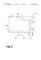
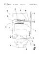
- FIG. 1is a perspective view of a portion of a circuit board including an assembly of transceivers thereon in accordance with the present invention.
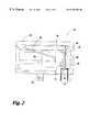
- FIG. 2is a longitudinal cross-sectional view of one of the transceivers as shown in FIG. 1 .
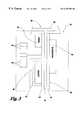
- FIG. 3is a schematic view, partially in section, of the shown in FIG. 2 .
- FIG. 4is a front elevational view of the transceivers as shown in FIG. 2 .
- FIG. 5is a side elevational view of the transceivers as shown in FIG. 2 .
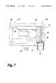
- FIG. 6is a bottom plan view of the transceiver as shown in FIG. 2 .
- FIG. 7is a longitudinal cross-sectional view of an optical version of a transceiver in accordance with the present invention.
- FIG. 8is a schematic view, partially in section, of the transceiver shown in FIG. 7 .
- FIG. 9is a front elevational view of the transceiver as shown in FIG. 7 .
- FIG. 10is a front elevational view of another embodiment of an assembly of transceivers as shown in FIG. 7 .
- FIG. 11is a schematic side view, partially in section, of another embodiment of the transceiver in accordance with the present invention.
- An assembly or module 26 of communications transceivers 25 in accordance with the present inventionis illustrated in the communications system portion 20 of FIG. 1 .
- the assembly 26is mounted on a mother circuit board 27 as will be readily appreciated by those skilled in the art.
- Each of the transceivers 25may receive a mating plug 31 .
- the mating plug 31is, in turn, connected to a cable 32 which may include copper wires, such as in the form of one or more twisted pairs of wires.
- the cable 32may also contain one or more optical fibers, such as a pair of optical fibers, as will be readily appreciated by those skilled in the art.
- the transceiver 25includes a jack housing 33 including portions defining a recess 34 for receiving a mating plug 31 therein.
- the jack housing 33is preferably molded plastic as will be readily appreciated by those skilled in the art.
- signal connector meansin the form of a plurality of electrical contacts or conductors 36 are mounted within the recess 34 for establishing inbound and outbound signal paths with corresponding signal conductors of the mating plug 31 , as will be readily appreciated by those skilled in the art.
- the conductors 36are typically biased downwardly to engage corresponding conductors of the plug as will also be readily appreciated by those skilled in the art.
- a circuit board 38is positioned within the jack housing 33 and traces or conductive paths on the circuit board are connected to the conductors 36 .
- the circuit board 38is positioned to extend in a vertical orientation spanning the full dimensions of the interior of the jack housing 33 .
- the circuit board 38illustratively includes an electrically conductive layer 42 sandwiched between first and second dielectric layers 43 thereby defining a first internal electromagnetic interference (EMI) shield.
- EMIelectromagnetic interference
- Other conductive tracesare typically provided on the outer surfaces of the dielectric layers 43 as will be readily appreciated by those skilled in the art.
- electrical connectionsmay be established extending through the first internal EMI shield 42 .
- the jack housing 33is preferably compatible in size and shape with an RJ-45 jack as will be appreciated by those skilled in the art.
- the transceiver 25illustratively includes a plurality of electrically conductive pins 47 connected to the circuit board 38 and extending outwardly from the jack housing 33 in an arrangement compatible with an RJ-45 jack transceiver.
- the pins 47may extend generally parallel to the circuit board 38 and in two rows as shown perhaps best in the bottom plan view of FIG. 6 .
- the transceiver 25also includes stake posts 53 to facilitate mounting to the mother circuit board 27 , for example, and as will be readily appreciated by those skilled in the art.
- the transceiver 25may also include an electrically conductive layer 50 on outer surface portions of the jack housing 33 defining an external EMI shield. As shown schematically in FIG. 3, the first internal EMI shield 42 may be electrically connected to the external EMI shield 50 . The external EMI shield 50 may be connected to the mother circuit board 27 via the illustrated pins 56 .
- At least one first circuit device being susceptible to EMIis mounted on a first side of the circuit board 38
- at least one second circuit device generating EMIis mounted on the circuit board on a second side thereof opposite the first side.
- the first internal EMI shield 42extends between the at least one first circuit device and the at least one second circuit device.
- the EMI susceptible device or componentis an active circuit, such as in the form of the illustrated active integrated circuit 45 .
- the active IC 45performs a number of functions according to the respective communications protocol being implemented; however, it typically includes a high gain amplifier stage that is susceptible to EMI, for example.
- the active IC 45performs analog-to-digital conversion of the inbound signal, and digital-to-analog conversion of the outbound signal, so that only digital signals are routed to and processed by the mother circuit board 27 (FIG. 1 ).
- the active IC 45may perform amplification, analog-to-digital and/or digital-to-analog conversion.
- the active IC 45may accept a digital input signal and produce a digital output signal so that no analog signals are carried on the external mother board.
- the at least one second circuit devicecomprises at least one magnetic device 60 .
- the magnetic devices or magnetics 60typically includes transformers as will be readily understood by those skilled in the art.
- the first internal EMI shield 42is positioned to extend between the EMI susceptible active IC 45 and the relatively high EMI generating magnetics 60 .
- the relative positions of the active device 45 and the magnetics 60could be switched to be on reversed sides of the circuit board 38 in another embodiment of the invention.
- This internal EMI shield 42provides a compact arrangement for an RJ-45 compatible transceiver 25 .
- the internal shield in the form of the electrically conductive layer 42 of the mounting circuit board 38greatly simplifies assembly—particularly as compared to one or more separately installed shields for the magnetics 60 . In other words, an assembler need not fumble with a relatively small shield to ensure its correct placement in the jack housing 33 .
- the communications transceiver 25may include at least one filter/termination device 62 mounted on the circuit board 38 adjacent the at least one active device 45 .
- the filter/termination device 62is on the same side of the circuit board 38 as the active IC 45 .
- an electrically conductive member 63may be provided defining a second internal EMI shield between the at least one filter/termination device 62 and the at least one active device 45 .
- the transceiver 25 ′communicates over a pair of optical fibers as will be readily appreciated by those skilled in the art.
- the signal path connector meanscomprises an optical detector 70 for inbound optical signals, and an optical emitter 71 for outbound optical signals as shown schematically in FIG. 8 .
- at least one first circuit device that is susceptible to EMIis a receiver circuit device, such as a receiver IC 73 , connected to the optical detector 70 .
- the receiver IC 73typically includes high gain amplification circuitry that is susceptible to EMI.
- other signal processing circuitrymay also be susceptible to EMI as will also be readily appreciated by those skilled in the art.
- the at least one second circuit device in this optical embodiment of the communications transceiver 25 ′also illustratively includes a transmitter circuit device connected to the optical emitter 71 .
- the transmitter deviceis illustratively in the form of a transmitter IC 74 .
- the first internal EMI shield 42 ′reduces undesired coupling of EMI from the high speed, high power circuitry of the transmitter IC 74 from interfering with the high gain amplification and signal processing circuitry of the receiver IC 73 . While the transmitter IC 74 is shown on the inside of the circuit board 38 ′ and the receiver IC 73 is on the outside, these relative positions could be reversed, as long as these devices are on opposite sides of the first internal EMI shield 42 ′. Electrical conductors 36 ′ are shown in the illustrated embodiment, but may be deleted in other embodiments of the invention as will be appreciated by those skilled in the art.
- FIGS. 7-10 labeled with prime notationare similar to those elements described above with respect to the twisted pair embodiment of the communications transceiver 25 . Accordingly, these elements require no further description herein to those skilled in the art.
- FIG. 10an assembly or module 75 of communications transceivers 25 ′ is shown.
- the illustrated assembly 75 of transceivers 25 ′includes twelve transceivers arranged in upper and lower groups of six transceivers each. Such an assembly could be provided in other multiples, such as the quad-pack assembly illustrated in FIG. 1 .
- FIG. 10an assembly or module 75 of communications transceivers 25 ′ is shown.
- the illustrated assembly 75 of transceivers 25 ′includes twelve transceivers arranged in upper and lower groups of six transceivers each.
- Such an assemblycould be provided in other multiples, such as the quad-pack assembly illustrated in FIG. 1 .
- those of skill in the artwill appreciate that other configurations are also contemplated by the present invention.
- the transceiver 25 ′′is mounted on a mother circuit board 27 ′′.
- the transceiver 25 ′′includes a schematically illustrated generic first circuit device 77 that is susceptible to EMI, and a second generic circuit device 78 that is a generator of EMI.
- the first circuit device 77is separated from the second circuit device 78 by the intervening EMI shield 42 ′′ which is advantageously provided as part of the circuit board 38 ′′.
- the EMI shield 42 ′′is preferably connected to a ground on the mother circuit board 37 ′′ as will also be appreciated by those skilled in the art.
- the transceiver housing 33 ′′is compatible with the RJ-45 jack as will be readily appreciated by those skilled in the art, and can receive the mating plug 31 ′′. Those other elements indicated with double prime notation are similar to those already described and need no further explanation.
- a method aspect of the inventionis for making a communications transceiver 25 of a type comprising a jack housing 33 including portions defining a recess 34 for receiving a mating plug 31 therein, signal connector means within the recess for establishing inbound and outbound signal paths with corresponding signal connector means of the mating plug, and a circuit board 38 within the jack housing and connected to the signal connector means.
- the methodpreferably comprises the steps of: providing the circuit board 38 with an electrically conductive layer 42 defining a first internal electromagnetic interference (EMI) shield; positioning at least one first circuit device, such as an active IC 45 , being susceptible to EMI on a first side of the circuit board; and positioning at least one second circuit device generating EMI, such as the magnetics 60 , on the circuit board on a second side thereof opposite the first side so that the first internal EMI shield extends between the at least one first circuit device and the at least one second circuit device.
- EMIelectromagnetic interference
- the methodmay also include the steps of providing an electrically conductive layer 50 on outer surface portions of the jack housing 33 defining an external EMI shield, and electrically connecting the first internal EMI shield 42 to the external EMI shield 50 .
- the jack housing 33 and output pins 47are compatible with an RJ-45 jack.
Landscapes
- Shielding Devices Or Components To Electric Or Magnetic Fields (AREA)
- Details Of Connecting Devices For Male And Female Coupling (AREA)
Abstract
Description
Claims (23)
Priority Applications (6)
| Application Number | Priority Date | Filing Date | Title |
|---|---|---|---|
| US09/098,277US6497588B1 (en) | 1998-06-16 | 1998-06-16 | Communications transceiver with internal EMI shield and associated methods |
| US09/137,407US6308235B1 (en) | 1998-06-16 | 1998-08-20 | Multi-port communications device and associated methods |
| AU45685/99AAU4568599A (en) | 1998-06-16 | 1999-06-15 | Multi-port communications device and associated methods |
| PCT/US1999/013491WO1999066604A1 (en) | 1998-06-16 | 1999-06-15 | Multi-port communications device and associated methods |
| US09/333,334US6324610B1 (en) | 1998-06-16 | 1999-06-15 | Shared multi-port communications device and associated methods |
| US09/333,462US6344969B1 (en) | 1998-06-16 | 1999-06-15 | Switched multi-port communications device and associated methods |
Applications Claiming Priority (1)
| Application Number | Priority Date | Filing Date | Title |
|---|---|---|---|
| US09/098,277US6497588B1 (en) | 1998-06-16 | 1998-06-16 | Communications transceiver with internal EMI shield and associated methods |
Related Child Applications (2)
| Application Number | Title | Priority Date | Filing Date |
|---|---|---|---|
| US09/137,407Continuation-In-PartUS6308235B1 (en) | 1998-06-16 | 1998-08-20 | Multi-port communications device and associated methods |
| US09/137,407ContinuationUS6308235B1 (en) | 1998-06-16 | 1998-08-20 | Multi-port communications device and associated methods |
Publications (1)
| Publication Number | Publication Date |
|---|---|
| US6497588B1true US6497588B1 (en) | 2002-12-24 |
Family
ID=22268576
Family Applications (1)
| Application Number | Title | Priority Date | Filing Date |
|---|---|---|---|
| US09/098,277Expired - Fee RelatedUS6497588B1 (en) | 1998-06-16 | 1998-06-16 | Communications transceiver with internal EMI shield and associated methods |
Country Status (1)
| Country | Link |
|---|---|
| US (1) | US6497588B1 (en) |
Cited By (23)
| Publication number | Priority date | Publication date | Assignee | Title |
|---|---|---|---|---|
| US20020154366A1 (en)* | 2001-04-24 | 2002-10-24 | Tomoharu Horio | Infrared data communication module and method of making the same |
| US20040149402A1 (en)* | 2003-01-30 | 2004-08-05 | Tzong-Fu Lin | Width-adjustable curtain track |
| US20050135727A1 (en)* | 2003-12-18 | 2005-06-23 | Sioptical, Inc. | EMI-EMC shield for silicon-based optical transceiver |
| US6957982B1 (en)* | 2004-08-05 | 2005-10-25 | Hon Hai Precision Ind. Co., Ltd. | Stacked modular jack |
| US6999323B1 (en) | 2002-10-17 | 2006-02-14 | Finisar Corporation | Electromagnetic interference containment transceiver module |
| US20070015416A1 (en)* | 2005-03-23 | 2007-01-18 | Gutierrez Aurelio J | Power-enabled connector assembly and method of manufacturing |
| US20070202752A1 (en)* | 2005-08-25 | 2007-08-30 | Telegaertner Karl Gaertner Gmbh | Electrical socket |
| US7300215B2 (en) | 2004-06-04 | 2007-11-27 | Industrial Technology Research Institute | Light transceiver module |
| US20080038963A1 (en)* | 2006-04-28 | 2008-02-14 | Kenichi Hirokawa | Receptacle connector and apparatus having the same |
| US7384300B1 (en)* | 1999-12-22 | 2008-06-10 | Xerox Corporation | Method and apparatus for a connection sensing apparatus |
| US20090081907A1 (en)* | 2007-09-22 | 2009-03-26 | Hon Hai Precision Ind. Co., Ltd. | Electrical connector having an improved housing having a curved structure |
| US20120040559A1 (en)* | 2010-08-16 | 2012-02-16 | Nai-Chien Chang | Connector having protection components |
| US20120171898A1 (en)* | 2010-12-30 | 2012-07-05 | Hon Hai Precision Industry Co., Ltd. | Modular jack with magnetic module od reduced profile |
| US8298922B2 (en) | 2008-12-19 | 2012-10-30 | Telegaertner Karl Gaertner Gmbh | Electrical plug connector |
| US20130084720A1 (en)* | 2011-09-30 | 2013-04-04 | Nai-Chien Chang | Network connector structure |
| US20140179163A1 (en)* | 2012-12-21 | 2014-06-26 | Hon Hai Precision Industry Co., Ltd. | Electrical connector |
| US20140242843A1 (en)* | 2013-02-22 | 2014-08-28 | Ya-Hui Huang | Signal transmission apparatus of connector |
| US9553392B2 (en) | 2014-03-28 | 2017-01-24 | Telegaertner Karl Gaertner Gmbh | Electrical plug connector having a plug-connection member and a cable outlet member |
| US9553402B2 (en) | 2014-03-28 | 2017-01-24 | Telegaertner Karl Gaertner Gmbh | Electrical plug connector with plug-in connection and cable outlet member |
| US9847607B2 (en) | 2014-04-23 | 2017-12-19 | Commscope Technologies Llc | Electrical connector with shield cap and shielded terminals |
| US20190319379A1 (en)* | 2018-04-11 | 2019-10-17 | Pegatron Corporation | High-rate signal connector module |
| CN114709675A (en)* | 2021-12-13 | 2022-07-05 | 陕西航空电气有限责任公司 | Electromagnetic compatibility shielding bush of power socket |
| US20240210640A1 (en)* | 2022-12-27 | 2024-06-27 | Fujin Precision Industrial (Jincheng)Co.,Ltd. | Adapter, connector, and opto-electric transmission assembly |
Citations (10)
| Publication number | Priority date | Publication date | Assignee | Title |
|---|---|---|---|---|
| US5518423A (en) | 1994-07-19 | 1996-05-21 | The Siemon Company | Shielded connector assembly |
| US5647767A (en)* | 1995-02-06 | 1997-07-15 | The Whitaker Corporation | Electrical connector jack assembly for signal transmission |
| US5687233A (en)* | 1996-02-09 | 1997-11-11 | Maxconn Incorporated | Modular jack having built-in circuitry |
| US6135819A (en)* | 1999-05-19 | 2000-10-24 | Lin; Chang-Liang | Telecommunication socket capable of directly inserting or connecting with a modularized circuit |
| US6179668B1 (en)* | 1999-06-22 | 2001-01-30 | Chin-Mao Kan | Electric connector including a circuit board |
| US6224425B1 (en)* | 1998-04-20 | 2001-05-01 | Pulse Engineering, Inc. | Simplified microelectronic connector and method of manufacturing |
| US6328595B1 (en)* | 2001-04-27 | 2001-12-11 | Speed Tech Corp. | Electric connector |
| US6409548B1 (en)* | 2000-11-02 | 2002-06-25 | Pulse Engineering, Inc. | Microelectronic connector with open-cavity insert |
| US6428361B1 (en)* | 1999-05-24 | 2002-08-06 | Stewart Connector Systems, Inc. | Surface mountable connector assembly including a printed circuit board |
| US6450837B1 (en)* | 2001-10-29 | 2002-09-17 | Hon Hai Precision Ind. Co., Ltd. | Electrical connector having surge suppressing device |
- 1998
- 1998-06-16USUS09/098,277patent/US6497588B1/ennot_activeExpired - Fee Related
Patent Citations (10)
| Publication number | Priority date | Publication date | Assignee | Title |
|---|---|---|---|---|
| US5518423A (en) | 1994-07-19 | 1996-05-21 | The Siemon Company | Shielded connector assembly |
| US5647767A (en)* | 1995-02-06 | 1997-07-15 | The Whitaker Corporation | Electrical connector jack assembly for signal transmission |
| US5687233A (en)* | 1996-02-09 | 1997-11-11 | Maxconn Incorporated | Modular jack having built-in circuitry |
| US6224425B1 (en)* | 1998-04-20 | 2001-05-01 | Pulse Engineering, Inc. | Simplified microelectronic connector and method of manufacturing |
| US6135819A (en)* | 1999-05-19 | 2000-10-24 | Lin; Chang-Liang | Telecommunication socket capable of directly inserting or connecting with a modularized circuit |
| US6428361B1 (en)* | 1999-05-24 | 2002-08-06 | Stewart Connector Systems, Inc. | Surface mountable connector assembly including a printed circuit board |
| US6179668B1 (en)* | 1999-06-22 | 2001-01-30 | Chin-Mao Kan | Electric connector including a circuit board |
| US6409548B1 (en)* | 2000-11-02 | 2002-06-25 | Pulse Engineering, Inc. | Microelectronic connector with open-cavity insert |
| US6328595B1 (en)* | 2001-04-27 | 2001-12-11 | Speed Tech Corp. | Electric connector |
| US6450837B1 (en)* | 2001-10-29 | 2002-09-17 | Hon Hai Precision Ind. Co., Ltd. | Electrical connector having surge suppressing device |
Non-Patent Citations (3)
| Title |
|---|
| Product Sheet H309.A, "Fastpulse High Speed LAN Transceivers", Pulse, (7/96), pp. 1-4. |
| Product Sheet MD6301 Series, "Single 10/100BASE-TX Filtered Connector Module", Valor Electronics, Inc., 1997. |
| Product Sheet MD6304 Series, "Quad 10/100BASE-TX Filtered Connector Module", Valor Electronics, Inc., 1997. |
Cited By (36)
| Publication number | Priority date | Publication date | Assignee | Title |
|---|---|---|---|---|
| US20080196519A1 (en)* | 1999-12-22 | 2008-08-21 | Xerox Corporation | Method and apparatus for a connection sensing apparatus |
| US7384300B1 (en)* | 1999-12-22 | 2008-06-10 | Xerox Corporation | Method and apparatus for a connection sensing apparatus |
| US7814240B2 (en) | 1999-12-22 | 2010-10-12 | Xerox Corporation | Method and apparatus for a connection sensing apparatus |
| US7263294B2 (en)* | 2001-04-24 | 2007-08-28 | Rohm Co., Ltd. | Infrared data communication module and method of making the same |
| US20020154366A1 (en)* | 2001-04-24 | 2002-10-24 | Tomoharu Horio | Infrared data communication module and method of making the same |
| US6999323B1 (en) | 2002-10-17 | 2006-02-14 | Finisar Corporation | Electromagnetic interference containment transceiver module |
| US7068522B2 (en) | 2002-10-17 | 2006-06-27 | Finisar Corporation | EMI containment transceiver module with floating PCB |
| US7286372B2 (en) | 2002-10-17 | 2007-10-23 | Finisar Corporation | Transceiver module with PCB having embedded traces for EMI control |
| US20040149402A1 (en)* | 2003-01-30 | 2004-08-05 | Tzong-Fu Lin | Width-adjustable curtain track |
| US20050135727A1 (en)* | 2003-12-18 | 2005-06-23 | Sioptical, Inc. | EMI-EMC shield for silicon-based optical transceiver |
| US7300215B2 (en) | 2004-06-04 | 2007-11-27 | Industrial Technology Research Institute | Light transceiver module |
| US7680389B2 (en) | 2004-06-04 | 2010-03-16 | Industrial Technology Research Institute | Light transceiver module |
| US6957982B1 (en)* | 2004-08-05 | 2005-10-25 | Hon Hai Precision Ind. Co., Ltd. | Stacked modular jack |
| US20070015416A1 (en)* | 2005-03-23 | 2007-01-18 | Gutierrez Aurelio J | Power-enabled connector assembly and method of manufacturing |
| US7524206B2 (en) | 2005-03-23 | 2009-04-28 | Pulse Engineering, Inc. | Power-enabled connector assembly with heat dissipation apparatus and method of manufacturing |
| US20070202752A1 (en)* | 2005-08-25 | 2007-08-30 | Telegaertner Karl Gaertner Gmbh | Electrical socket |
| US20080038963A1 (en)* | 2006-04-28 | 2008-02-14 | Kenichi Hirokawa | Receptacle connector and apparatus having the same |
| US7841908B2 (en)* | 2007-09-22 | 2010-11-30 | Hon Hai Precision Ind. Co., Ltd. | Electrical connector having an improved housing having a curved structure |
| US20090081907A1 (en)* | 2007-09-22 | 2009-03-26 | Hon Hai Precision Ind. Co., Ltd. | Electrical connector having an improved housing having a curved structure |
| US8298922B2 (en) | 2008-12-19 | 2012-10-30 | Telegaertner Karl Gaertner Gmbh | Electrical plug connector |
| US20120040559A1 (en)* | 2010-08-16 | 2012-02-16 | Nai-Chien Chang | Connector having protection components |
| US8152564B2 (en)* | 2010-08-16 | 2012-04-10 | Nai-Chien Chang | Connector having protection components |
| US20120171898A1 (en)* | 2010-12-30 | 2012-07-05 | Hon Hai Precision Industry Co., Ltd. | Modular jack with magnetic module od reduced profile |
| US8439711B2 (en)* | 2010-12-30 | 2013-05-14 | Hon Hai Precision Industry Co., Ltd. | Modular jack with magnetic module od reduced profile |
| US20130084720A1 (en)* | 2011-09-30 | 2013-04-04 | Nai-Chien Chang | Network connector structure |
| US8529297B2 (en)* | 2011-09-30 | 2013-09-10 | Nai-Chien Chang | Network connector structure |
| US20140179163A1 (en)* | 2012-12-21 | 2014-06-26 | Hon Hai Precision Industry Co., Ltd. | Electrical connector |
| US9077120B2 (en)* | 2012-12-21 | 2015-07-07 | Hon Hai Precision Industry Co., Ltd. | Electrical connector |
| US20140242843A1 (en)* | 2013-02-22 | 2014-08-28 | Ya-Hui Huang | Signal transmission apparatus of connector |
| US9553392B2 (en) | 2014-03-28 | 2017-01-24 | Telegaertner Karl Gaertner Gmbh | Electrical plug connector having a plug-connection member and a cable outlet member |
| US9553402B2 (en) | 2014-03-28 | 2017-01-24 | Telegaertner Karl Gaertner Gmbh | Electrical plug connector with plug-in connection and cable outlet member |
| US9847607B2 (en) | 2014-04-23 | 2017-12-19 | Commscope Technologies Llc | Electrical connector with shield cap and shielded terminals |
| US10476212B2 (en) | 2014-04-23 | 2019-11-12 | Commscope Technologies Llc | Electrical connector with shield cap and shielded terminals |
| US20190319379A1 (en)* | 2018-04-11 | 2019-10-17 | Pegatron Corporation | High-rate signal connector module |
| CN114709675A (en)* | 2021-12-13 | 2022-07-05 | 陕西航空电气有限责任公司 | Electromagnetic compatibility shielding bush of power socket |
| US20240210640A1 (en)* | 2022-12-27 | 2024-06-27 | Fujin Precision Industrial (Jincheng)Co.,Ltd. | Adapter, connector, and opto-electric transmission assembly |
Similar Documents
| Publication | Publication Date | Title |
|---|---|---|
| US6497588B1 (en) | Communications transceiver with internal EMI shield and associated methods | |
| US6431764B1 (en) | Optical transceiver RJ-jack with EMI shield | |
| US6113422A (en) | Connector with circuit devices and indicators | |
| KR950007425B1 (en) | Electrical connectors | |
| US6464529B1 (en) | Connector element for high-speed data communications | |
| EP2089889B1 (en) | Modular connector with reduced termination variability | |
| US5639266A (en) | High frequency electrical connector | |
| US5687233A (en) | Modular jack having built-in circuitry | |
| US6612871B1 (en) | Electrical connector having integral noise suppressing device | |
| US6116946A (en) | Surface mounted modular jack with integrated magnetics and LEDS | |
| US6425781B1 (en) | RJ jack with integrated interface magnetics | |
| US6623307B2 (en) | High frequency modular jack connector | |
| US6165018A (en) | Connector having internal crosstalk compensation | |
| US20110053418A1 (en) | Modular jack with two-piece housing and insert | |
| US7264516B2 (en) | Communications jack with printed wiring board having paired coupling conductors | |
| US6344969B1 (en) | Switched multi-port communications device and associated methods | |
| US5340333A (en) | Shielded modular adapter | |
| US7261592B2 (en) | Electrical connector | |
| US20030186591A1 (en) | Connector element for high-speed data communications | |
| EP1815607B1 (en) | Crosstalk reducing contact configuration in a communication system | |
| JP4582961B2 (en) | Tuner with no RF input pin / lead on edge | |
| US7285025B2 (en) | Enhanced jack with plug engaging printed circuit board | |
| US20050070161A1 (en) | Modular jack with external electromagnetic shielding | |
| CA2228016A1 (en) | Connector cover with integral terminator | |
| WO1999066604A9 (en) | Multi-port communications device and associated methods |
Legal Events
| Date | Code | Title | Description |
|---|---|---|---|
| AS | Assignment | Owner name:POLYCORE TECHNOLOGIES, FLORIDA Free format text:ASSIGNMENT OF ASSIGNORS INTEREST;ASSIGNORS:SCHARF, ROBERT M.;LORD, RANDAL B.;REEL/FRAME:009255/0096;SIGNING DATES FROM 19980610 TO 19980612 | |
| FEPP | Fee payment procedure | Free format text:PAT HOLDER NO LONGER CLAIMS SMALL ENTITY STATUS, ENTITY STATUS SET TO UNDISCOUNTED (ORIGINAL EVENT CODE: STOL); ENTITY STATUS OF PATENT OWNER: LARGE ENTITY | |
| AS | Assignment | Owner name:STRATOS MICRO SYSTEMS, INC., FLORIDA Free format text:ASSIGNMENT OF ASSIGNORS INTEREST;ASSIGNOR:METHODE ELECTRONICS OF FLORIDA, INC.;REEL/FRAME:010959/0031 Effective date:19990915 Owner name:METHODE COMMUNICATIONS MODULES, INC., FLORIDA Free format text:ASSIGNMENT OF ASSIGNORS INTEREST;ASSIGNOR:METHODE ELECTRONICS OF FLORIDA, INC.;REEL/FRAME:010959/0031 Effective date:19990915 | |
| AS | Assignment | Owner name:METHODE FLORIDA, INC., FLORIDA Free format text:ASSIGNMENT AND CHANGE OF NAME;ASSIGNOR:POLYCORE TECHNOLOGIES, INC.;REEL/FRAME:010978/0560 Effective date:19990414 Owner name:METHODE COMMUNICATION MODULES, INC., FLORIDA Free format text:ASSIGNMENT AND CHANGE OF NAME;ASSIGNOR:POLYCORE TECHNOLOGIES, INC.;REEL/FRAME:010978/0560 Effective date:19990414 Owner name:STRATOS MICRO SYSTEMS, INC., FLORIDA Free format text:ASSIGNMENT AND CHANGE OF NAME;ASSIGNOR:POLYCORE TECHNOLOGIES, INC.;REEL/FRAME:010978/0560 Effective date:19990414 | |
| FPAY | Fee payment | Year of fee payment:4 | |
| REMI | Maintenance fee reminder mailed | ||
| LAPS | Lapse for failure to pay maintenance fees | ||
| STCH | Information on status: patent discontinuation | Free format text:PATENT EXPIRED DUE TO NONPAYMENT OF MAINTENANCE FEES UNDER 37 CFR 1.362 |