US6496876B1 - System and method for storing a tag to identify a functional storage location in a memory device - Google Patents
System and method for storing a tag to identify a functional storage location in a memory deviceDownload PDFInfo
- Publication number
- US6496876B1 US6496876B1US09/217,781US21778198AUS6496876B1US 6496876 B1US6496876 B1US 6496876B1US 21778198 AUS21778198 AUS 21778198AUS 6496876 B1US6496876 B1US 6496876B1
- Authority
- US
- United States
- Prior art keywords
- storage location
- tag
- dysfunctional
- address
- memory
- Prior art date
- Legal status (The legal status is an assumption and is not a legal conclusion. Google has not performed a legal analysis and makes no representation as to the accuracy of the status listed.)
- Expired - Fee Related
Links
- 238000000034methodMethods0.000titleclaimsdescription33
- 238000012545processingMethods0.000description11
- 230000002950deficientEffects0.000description8
- 238000010420art techniqueMethods0.000description5
- 230000009286beneficial effectEffects0.000description5
- 238000013500data storageMethods0.000description3
- 230000006870functionEffects0.000description3
- 238000003780insertionMethods0.000description2
- 230000037431insertionEffects0.000description2
- 238000004519manufacturing processMethods0.000description1
- 238000013507mappingMethods0.000description1
- 239000000463materialSubstances0.000description1
- 230000003287optical effectEffects0.000description1
- 230000002093peripheral effectEffects0.000description1
- 239000004065semiconductorSubstances0.000description1
- 239000007787solidSubstances0.000description1
- 238000012360testing methodMethods0.000description1
- 238000012546transferMethods0.000description1
Images


Classifications
- G—PHYSICS
- G11—INFORMATION STORAGE
- G11C—STATIC STORES
- G11C29/00—Checking stores for correct operation ; Subsequent repair; Testing stores during standby or offline operation
- G11C29/70—Masking faults in memories by using spares or by reconfiguring
- G11C29/88—Masking faults in memories by using spares or by reconfiguring with partially good memories
- G—PHYSICS
- G11—INFORMATION STORAGE
- G11C—STATIC STORES
- G11C29/00—Checking stores for correct operation ; Subsequent repair; Testing stores during standby or offline operation
- G11C29/04—Detection or location of defective memory elements, e.g. cell constructio details, timing of test signals
- G11C29/08—Functional testing, e.g. testing during refresh, power-on self testing [POST] or distributed testing
- G11C29/12—Built-in arrangements for testing, e.g. built-in self testing [BIST] or interconnection details
- G11C29/44—Indication or identification of errors, e.g. for repair
- G—PHYSICS
- G11—INFORMATION STORAGE
- G11C—STATIC STORES
- G11C29/00—Checking stores for correct operation ; Subsequent repair; Testing stores during standby or offline operation
- G11C29/70—Masking faults in memories by using spares or by reconfiguring
- G11C29/88—Masking faults in memories by using spares or by reconfiguring with partially good memories
- G11C29/883—Masking faults in memories by using spares or by reconfiguring with partially good memories using a single defective memory device with reduced capacity, e.g. half capacity
Definitions
- the inventionrelates generally to the use of partially defective memory devices and, in particular, to the use of partially defective random access memory (RAM) devices.
- RAMrandom access memory
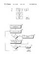
- a system 100 capable of using partially defective memory 102may also include application 104 (e.g., an audio or video storage application), interface 106 through which application 104 communicates with memory 102 , and input-output (I/O) unit 108 through which application 104 communicates with external units or users.
- application 104e.g., an audio or video storage application
- interface 106through which application 104 communicates with memory 102
- I/O unit 108input-output unit 108 through which application 104 communicates with external units or users.
- interface 106may generate a table whose entries identify blocks within memory 102 that have one or more defective locations.
- a block of memorymay be a specified number of memory locations, for example, 256 bits, 64 nibbles, 128 bytes, or 64 words.
- interface 106may write a known pattern (e.g., the zero value) to every location in memory 102 (at 200 ).
- a block of memory 102may be read (at 202 ) and inspected (at 204 ). If every location retrieved at 202 reflects the pattern written at 200 (the ‘yes’ prong at 204 ), a table entry is generated that identifies the block of memory as valid (at 206 ).
- a table entryis generated that identifies the entire block of memory as invalid (at 208 ). If, after creating a table entry at 206 or 208 , the entire memory has been inspected (the ‘yes’ prong at 210 ), processing terminates (at 212 ). If, after creating a table entry at 206 or 208 , the entire memory has not been inspected (the ‘no’ prong at 210 ), processing continues at 202 . During subsequent operations, interface 106 may read information from and write information to memory 102 while skipping those blocks identified in the table as invalid. A table created in accordance with FIG.
- the tablemay be generated upon system 100 power-up/reset, or once during the manufacture and testing process. Further, the table may be stored in volatile memory such as RAM or nonvolatile memory such as programmable read only memory (PROM), electrically erasable programmable read only memory (EEPROM), or FLASH type memory.
- volatile memorysuch as RAM or nonvolatile memory such as programmable read only memory (PROM), electrically erasable programmable read only memory (EEPROM), or FLASH type memory.
- interface 106may write a pattern to memory 102 indicating whether a block is valid/functional or invalid/nonfunctional.
- interface 106may write a known pattern (e.g., the zero value) to every location in memory 102 (at 300 ).
- Memory 102may then be read back a block at a time (at 302 ) and inspected (at 304 ). If every location retrieved at 302 reflects the pattern written at 300 (the ‘yes’ prong at 304 ), each location in that block of memory is written with a specified pattern indicating it as valid memory (at 306 ).
- each location retrieved at 302does not match the pattern written at 300 (the ‘no’ prong at 304 ), each location in that block of memory is written with a specified pattern indicating it as invalid memory (at 308 ). If, after storing a pattern to memory at 306 or 308 , the entire memory has been inspected (the ‘yes’ prong at 310 ), processing terminates (at 312 ). If, after storing a pattern to memory at 306 or 308 , the entire memory has not been inspected (the ‘no’ prong at 310 ), processing continues at 302 . During subsequent operations, interface 106 may read information from and write information to memory 102 by skipping over those blocks marked as invalid.
- the inventionprovides a method to demarcate regions of dysfunctional storage locations in a memory device.
- the methodincludes identifying a first and a second dysfunctional storage location in the memory device, and storing a first tag before the first storage location, the first tag indicating a storage location immediately after the second storage location.
- the inventionalso provides a method to demarcate functional regions of storage locations by identifying a functional storage location, and storing a second tag at the identified functional storage location, the second tag indicating a storage location immediately preceding the first identified dysfunctional storage location.
- Methods in accordance with the inventionmay be stored in any media that is readable and executable by a programmable control device such as, for example, a microprocessor or custom designed state machine.
- FIG. 1shows a prior art system that may use partially defective memory devices.
- FIG. 2shows one prior art method to identify blocks within a memory device that include defective storage locations.
- FIG. 3shows another prior art method that identifies blocks within a memory device that include defective storage locations.
- FIG. 4shows a system in accordance with one embodiment of the invention.
- FIG. 5illustrates a memory device having regions of nonfunctional storage elements.
- FIG. 6shows one method in accordance with the invention to identify and demarcate memory regions having dysfunctional storage elements.
- FIG. 7illustrates a memory device having regions of nonfunctional storage elements demarcated by tags in accordance with one embodiment of the invention.
- FIG. 8shows a tag structure in accordance with one embodiment of the invention.
- FIG. 9illustrates a memory device having regions of nonfunctional storage elements demarcated by tags in accordance with another embodiment of the invention.
- FIG. 10shows another tag structure in accordance with one embodiment of the invention.
- FIG. 11shows another method to identify and demarcate memory regions in accordance with one embodiment of the invention.
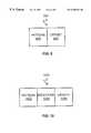
- a system 400 in accordance with one embodiment of the inventionincludes audio application 402 , analog to digital (ADC) 404 and digital to analog (DAC) 406 converters, memory interface unit 408 , and audio random access memory (ARAM) 410 .
- Audio application 402may include a combination of hardware and software needed to implement the target application. For example, if the target application is a telephone answering device, audio application 402 may include a microprocessor, programmable microcontroller, or a custom designed state machine to implement the desired answering machine functions.
- Analog to digital converter 404provides a mechanism for externally generated sound (e.g., a voice) to be changed to a digital format for processing and/or storage in system 400 .
- DAC 406provides a mechanism for digitally generated and/or stored information to be converted to analog format for external presentation.
- Interface 408provides a mechanism for interfacing application 402 to memory 410 .
- interface 408may include a Z 8 microcontroller manufactured by the Zilog corporation.
- memory 410includes two 4M ⁇ 4 ARAM devices to provide a total of 4 megabytes (MB) of memory, e.g., two S4004SA1-0 memory devices sold by Micron Electronics Incorporated.
- One function of interface unit 408is to present a uniform memory space to application 402 , mapping out any nonfunctional memory locations in memory 410 . That is, interface 408 makes any nonfunctional memory locations in memory 410 transparent to application 402 .
- memory 410may be visualized as a contiguous sequence of memory locations (each 8 bits, or 1 byte, wide) starting at 000000h (where ‘h’ indicates hexadecimal notation) and ending at 3FFFFFh (4 ⁇ 2 20 bytes or 4 MB).
- memory 410is shown as having two regions of partially dysfunctional memory locations: region 1500 and region 2 502 (dysfunctional memory locations are represented by solid horizontal black bars).
- interface unit 408identifies and demarcates regions of memory 410 that include nonfunctional storage elements—storage locations (e.g., bytes) having one or more components (e.g., bits) that do not function correctly.
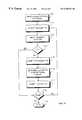
- interface 408may write a known pattern, such as the value 2 Ah, to each location in memory 410 (at 600 ).
- Interface 408may then read memory 410 (at 602 ), and determine if the pattern written at 600 is the same as the pattern read at 602 (at 604 ). If the patterns match (the ‘yes’ prong at 604 ), the memory location read at 602 is determined to be valid/functional, and processing continues at 610 .
- interface 408continues to read storage locations from memory 410 to determine the extent of the dysfunctional memory (at 608 ). Referring to FIG. 7, if the address of the first dysfunctional memory location is A, and the last dysfunctional storage location has an address of B, the extent of the dysfunctional storage locations is (B-A) and defines region 1500 . With the number of dysfunctional storage locations known (at 606 ), interface 408 may store tag T 1 700 preceding the region of bad memory (at 608 ), region 1500 for example.
- tag 700may include pattern portion 800 and offset portion 802 . It is beneficial if pattern portion 800 is selected to uniquely identify the combination of pattern portion 800 and offset portion 802 as a tag.
- tag pattern portion 800could be 32-bits represented by an 8-digit hexadecimal value, each of whose digits are not evenly divisible by two.
- One illustrative pattern portion 800is 35793579h.
- Tag offset portion 802may indicate the next valid storage location in memory 410 .
- offset portion 802may “point” to storage location B+1.
- An illustrative offset valuemay be embodied in a 16-bit value, making it possible to specify offsets as large as approximately 65,000 storage locations (e.g., bytes).
- interface 408determines if all of memory 410 has been inspected (at 610 ). If memory 410 has been inspected (the ‘yes’ prong at 610 ), processing terminates at 612 . If all of memory 410 has not been inspected (the ‘no’ prong at 610 ), processing continues at 602 . For example, referring again to FIG. 7, interface 408 may continue reading from memory 410 until address location C is inspected. At that point acts 606 and 608 are performed to insert tag T 2 702 .
- region 2 502illustrates an area of memory having some non-contiguous dysfunctional storage locations.
- interface 408may specify that if less than N contiguous storage locations are functional, the collection of storage locations are dysfunctional. That is, a dysfunctional region may be defined as that region between two sequences of functional storage locations, each of which are at least N storage locations in length.
- Nis set to a value equal to the size of a tag plus the minimum useful memory region.
- the smallest useable memory areato store data for example
- a tagis 4 bytes
- Nmay be greater than or equal to 20.
- memory regionsmay be demarcated with multiple tags.
- Header tags H 1 900 , H 2 902 , and H 3 904demarcate regions of memory 410 which include fully functional storage locations.
- Footer tags T 1 700 and T 2 702demarcate regions of memory 410 which include partially functional, or fully dysfunctional, storage locations.
- a header tag structure 1000 in accordance with one embodiment of the inventionmay include pattern portion 1002 , identifier portion 1004 , and length portion 1006 .
- pattern portion 1002is selected to uniquely identify header tag structure 1000 and which is different from tag pattern portion 800 .
- pattern portion 1002could be 32-bits represented by an 8-digit hexadecimal value, each of whose digits are not evenly divisible by two.
- One illustrative pattern portion 800is 97359735h.
- Tag identifier portion 1004may be used by interface 408 to identify which data is stored in the memory following the header tag.
- identifier portion 1004may be used by interface 408 to assist it in matching a symbolic reference for the tag's associated data (e.g., the symbol used by application 402 to identify the data).
- An illustrative identifier portion 1004may be embodied in a 16-bit value.
- tag length portion 1006may indicate the number of fully functional storage locations associated with a specified data item.
- tag length portion 1006may indicate the number of fully functional storage locations available for data storage following tag 1000 (i.e., until the next dysfunctional region or end of memory).
- An illustrative length portion 1006may be embodied in a 16-bit value.
- interface 408may initially write a known-pattern to each location in memory 410 (at 1100 ). Interface 408 may then initialize header tag structure 1000 at the start of memory 410 (at 1102 ). For example, interface 408 may write pattern portion 1002 to memory 410 and zeros' to identifier 1004 and length 1006 portions, This operation is generally possible as many ARAM devices (and other types of memory devices) guarantee the first M storage locations to be valid. For example, the S4004SA1-0 memory device sold by Micron Electronics, Incorporated guarantees that the first 16 storage locations are valid/functional.
- interface 408may read memory 410 (at 1104 ), and determine if the pattern written at 1100 is the same as the pattern read at 1104 (at 1106 ). If the two patterns match (the ‘yes’ prong at 1106 ), the memory location read at 1104 is determined to be valid/functional, and processing continues at 1114 .
- interface 408completes the header tag structure initialized at 1102 (at 1108 ) by, for example, writing to the tag's length portion 1006 the extent of the valid/functional storage location. Interface 408 may then continue to read storage locations from memory 410 to determine the extent of the dysfunctional memory (at 1110 ). With the number of dysfunctional storage locations known, interface 408 may insert a tag structure preceding the region of bad memory (at 1112 ), e.g., tag T 1 700 or tag T 2 702 in FIG. 9 .
- interface 408determines if all of memory 410 has been inspected (at 1114 ). If memory 410 has been inspected (the ‘yes’ prong at 1114 ), processing terminates at 1116 . If all of memory 410 has not been inspected (the ‘no’ prong at 1114 ), processing continues at 1102 .
- a method in accordance with the inventionmay map only out the one faulty location while also consuming a minimal amount of additional memory for a tag structure (or two tag structures if both a header and footer tag embodiment is used).
- techniques in accordance with the inventioneffectively increase the amount of memory available to a system (e.g., an application and/or memory interface) for data storage over prior art techniques.
- the inventionis not limited to audio or video applications—the invention may be used with any application that uses memory.
- partially dysfunctional high speed memory devicesmay be used in accordance with the invention in a system that can tolerate a less than maximum data transfer rate from memory (to accommodate the overhead of “skipping over” dysfunctional storage locations).
- the inventionmay be used in standard computer systems comprising a central processor, a main bus, a memory (e.g., system RAM), bridge circuits, and peripherals.
- acts in accordance with FIGS. 6 and 11may be performed by a programmable control device executing instructions organized into a program module.
- a programmable control devicemay be a computer processor or a custom designed state machine.
- Custom designed state machinesmay be embodied in a hardware device such as a printed circuit board comprising discrete logic, integrated circuits, or specially designed application specific integrated circuits (ASICs).
- Storage devices suitable for tangibly embodying program instructionsinclude all forms of non-volatile memory including, but not limited to: semiconductor memory devices such as EPROM, EEPROM, and flash devices; magnetic disks (fixed, floppy, and removable); other magnetic media such as tape; and optical media such as CD-ROM disks.
Landscapes
- Techniques For Improving Reliability Of Storages (AREA)
Abstract
Description
The invention relates generally to the use of partially defective memory devices and, in particular, to the use of partially defective random access memory (RAM) devices.
Not all applications that use computer memory devices require those devices to provide absolute store-and-retrieve fidelity. For example, applications such as telephone answering machines, some video storage devices, and toys may use memory devices that have one or more non-functional memory locations. Systems such as these may use a memory interface device to identify and map out those blocks of memory having one or more defective locations. Referring to FIG. 1, asystem 100 capable of using partiallydefective memory 102 may also include application104 (e.g., an audio or video storage application),interface 106 through whichapplication 104 communicates withmemory 102, and input-output (I/O)unit 108 through whichapplication 104 communicates with external units or users.
In one prior art technique,interface 106 may generate a table whose entries identify blocks withinmemory 102 that have one or more defective locations. A block of memory may be a specified number of memory locations, for example, 256 bits, 64 nibbles, 128 bytes, or 64 words. Referring to FIG. 2,interface 106 may write a known pattern (e.g., the zero value) to every location in memory102 (at200). Next, a block ofmemory 102 may be read (at202) and inspected (at204). If every location retrieved at202 reflects the pattern written at200 (the ‘yes’ prong at204), a table entry is generated that identifies the block of memory as valid (at206). If every location retrieved at202 does not match the pattern written at200 (the ‘no’ prong at204), a table entry is generated that identifies the entire block of memory as invalid (at208). If, after creating a table entry at206 or208, the entire memory has been inspected (the ‘yes’ prong at210), processing terminates (at212). If, after creating a table entry at206 or208, the entire memory has not been inspected (the ‘no’ prong at210), processing continues at202. During subsequent operations,interface 106 may read information from and write information tomemory 102 while skipping those blocks identified in the table as invalid. A table created in accordance with FIG. 1 may be generated uponsystem 100 power-up/reset, or once during the manufacture and testing process. Further, the table may be stored in volatile memory such as RAM or nonvolatile memory such as programmable read only memory (PROM), electrically erasable programmable read only memory (EEPROM), or FLASH type memory.
In another prior art technique,interface 106 may write a pattern tomemory 102 indicating whether a block is valid/functional or invalid/nonfunctional. Referring to FIG. 3,interface 106 may write a known pattern (e.g., the zero value) to every location in memory102 (at300).Memory 102 may then be read back a block at a time (at302) and inspected (at304). If every location retrieved at302 reflects the pattern written at300 (the ‘yes’ prong at304), each location in that block of memory is written with a specified pattern indicating it as valid memory (at306). If every location retrieved at302 does not match the pattern written at300 (the ‘no’ prong at304), each location in that block of memory is written with a specified pattern indicating it as invalid memory (at308). If, after storing a pattern to memory at306 or308, the entire memory has been inspected (the ‘yes’ prong at310), processing terminates (at312). If, after storing a pattern to memory at306 or308, the entire memory has not been inspected (the ‘no’ prong at310), processing continues at302. During subsequent operations,interface 106 may read information from and write information tomemory 102 by skipping over those blocks marked as invalid.
Current techniques to incorporate partially dysfunctional memory devices into a system include or exclude entire blocks of memory. Because the cost of memory is becoming increasingly important in driving the cost of finished products such as telephone answering machines, video storage devices, and toys, it would be beneficial to provide a mechanism that allows more of a partially dysfunctional memory device to be used.
In one embodiment, the invention provides a method to demarcate regions of dysfunctional storage locations in a memory device. The method includes identifying a first and a second dysfunctional storage location in the memory device, and storing a first tag before the first storage location, the first tag indicating a storage location immediately after the second storage location.
In another embodiment, the invention also provides a method to demarcate functional regions of storage locations by identifying a functional storage location, and storing a second tag at the identified functional storage location, the second tag indicating a storage location immediately preceding the first identified dysfunctional storage location.
Methods in accordance with the invention may be stored in any media that is readable and executable by a programmable control device such as, for example, a microprocessor or custom designed state machine.
FIG. 1 shows a prior art system that may use partially defective memory devices.
FIG. 2 shows one prior art method to identify blocks within a memory device that include defective storage locations.
FIG. 3 shows another prior art method that identifies blocks within a memory device that include defective storage locations.
FIG. 4 shows a system in accordance with one embodiment of the invention.
FIG. 5 illustrates a memory device having regions of nonfunctional storage elements.
FIG. 6 shows one method in accordance with the invention to identify and demarcate memory regions having dysfunctional storage elements.
FIG. 7 illustrates a memory device having regions of nonfunctional storage elements demarcated by tags in accordance with one embodiment of the invention.
FIG. 8 shows a tag structure in accordance with one embodiment of the invention.
FIG. 9 illustrates a memory device having regions of nonfunctional storage elements demarcated by tags in accordance with another embodiment of the invention.
FIG. 10 shows another tag structure in accordance with one embodiment of the invention.
FIG. 11 shows another method to identify and demarcate memory regions in accordance with one embodiment of the invention.
Techniques (including methods and devices) to map out those locations in a memory device determined to be faulty are described. Illustrative systems where such a technique may be beneficial include, but are not limited to, audio applications such as telephone answering machines and toys and video storage devices such as video disks. The following embodiments of this inventive concept are illustrative only and are not to be considered limiting in any respect.
Referring to FIG. 4, asystem 400 in accordance with one embodiment of the invention includesaudio application 402, analog to digital (ADC)404 and digital to analog (DAC)406 converters,memory interface unit 408, and audio random access memory (ARAM)410.Audio application 402 may include a combination of hardware and software needed to implement the target application. For example, if the target application is a telephone answering device,audio application 402 may include a microprocessor, programmable microcontroller, or a custom designed state machine to implement the desired answering machine functions. Analog todigital converter 404 provides a mechanism for externally generated sound (e.g., a voice) to be changed to a digital format for processing and/or storage insystem 400. Similarly,DAC 406 provides a mechanism for digitally generated and/or stored information to be converted to analog format for external presentation.Interface 408 provides a mechanism forinterfacing application 402 tomemory 410. For example,interface 408 may include a Z8 microcontroller manufactured by the Zilog corporation. In oneembodiment memory 410 includes two 4M×4 ARAM devices to provide a total of 4 megabytes (MB) of memory, e.g., two S4004SA1-0 memory devices sold by Micron Electronics Incorporated. One function ofinterface unit 408 is to present a uniform memory space toapplication 402, mapping out any nonfunctional memory locations inmemory 410. That is,interface 408 makes any nonfunctional memory locations inmemory 410 transparent toapplication 402.
Referring to FIG. 5,memory 410 may be visualized as a contiguous sequence of memory locations (each 8 bits, or 1 byte, wide) starting at 000000h (where ‘h’ indicates hexadecimal notation) and ending at 3FFFFFh (4×220bytes or 4 MB). For illustrative purposes,memory 410 is shown as having two regions of partially dysfunctional memory locations: region1500 and region2502 (dysfunctional memory locations are represented by solid horizontal black bars).
In accordance with one embodiment of the invention (see FIG.6),interface unit 408 identifies and demarcates regions ofmemory 410 that include nonfunctional storage elements—storage locations (e.g., bytes) having one or more components (e.g., bits) that do not function correctly. Initiallyinterface 408 may write a known pattern, such as the value2Ah, to each location in memory410 (at600).Interface 408 may then read memory410 (at602), and determine if the pattern written at600 is the same as the pattern read at602 (at604). If the patterns match (the ‘yes’ prong at604), the memory location read at602 is determined to be valid/functional, and processing continues at610.
If the pattern written at600 and read at602 do not match (the ‘no’ prong at604),interface 408 continues to read storage locations frommemory 410 to determine the extent of the dysfunctional memory (at608). Referring to FIG. 7, if the address of the first dysfunctional memory location is A, and the last dysfunctional storage location has an address of B, the extent of the dysfunctional storage locations is (B-A) and defines region1500. With the number of dysfunctional storage locations known (at606),interface 408 may storetag T1 700 preceding the region of bad memory (at608), region1500 for example.
Referring now to FIG. 8,tag 700 may includepattern portion 800 and offsetportion 802. It is beneficial ifpattern portion 800 is selected to uniquely identify the combination ofpattern portion 800 and offsetportion 802 as a tag. For example,tag pattern portion 800 could be 32-bits represented by an 8-digit hexadecimal value, each of whose digits are not evenly divisible by two. Oneillustrative pattern portion 800 is 35793579h. Tag offsetportion 802 may indicate the next valid storage location inmemory 410. For example, offsetportion 802 may “point” to storage location B+1. An illustrative offset value may be embodied in a 16-bit value, making it possible to specify offsets as large as approximately 65,000 storage locations (e.g., bytes).
Following a matched pattern at604 or a tag insertion at608,interface 408 determines if all ofmemory 410 has been inspected (at610). Ifmemory 410 has been inspected (the ‘yes’ prong at610), processing terminates at612. If all ofmemory 410 has not been inspected (the ‘no’ prong at610), processing continues at602. For example, referring again to FIG. 7,interface 408 may continue reading frommemory 410 until address location C is inspected. At that point acts606 and608 are performed to inserttag T2 702.
As shown in FIG. 7, region2502 illustrates an area of memory having some non-contiguous dysfunctional storage locations. When non-contiguous dysfunctional storage locations are encountered,interface 408 may specify that if less than N contiguous storage locations are functional, the collection of storage locations are dysfunctional. That is, a dysfunctional region may be defined as that region between two sequences of functional storage locations, each of which are at least N storage locations in length. As a practical matter, it is beneficial if N is set to a value equal to the size of a tag plus the minimum useful memory region. Thus, as an example, if the smallest useable memory area (to store data for example) is 16 bytes, and a tag is 4 bytes, then N may be greater than or equal to 20.
In accordance with another embodiment of the invention (see FIG.9), memory regions may be demarcated with multiple tags. Header tagsH1 900,H2 902, andH3 904 demarcate regions ofmemory 410 which include fully functional storage locations. Footer tagsT1 700 andT2 702 demarcate regions ofmemory 410 which include partially functional, or fully dysfunctional, storage locations.
Referring now to FIG. 10, aheader tag structure 1000 in accordance with one embodiment of the invention may includepattern portion 1002,identifier portion 1004, andlength portion 1006. As in the tag structure of FIG. 8, it may be beneficial ifpattern portion 1002 is selected to uniquely identifyheader tag structure 1000 and which is different fromtag pattern portion 800. For example,pattern portion 1002 could be 32-bits represented by an 8-digit hexadecimal value, each of whose digits are not evenly divisible by two. Oneillustrative pattern portion 800 is 97359735h.Tag identifier portion 1004 may be used byinterface 408 to identify which data is stored in the memory following the header tag. For example,identifier portion 1004 may be used byinterface 408 to assist it in matching a symbolic reference for the tag's associated data (e.g., the symbol used byapplication 402 to identify the data). Anillustrative identifier portion 1004 may be embodied in a 16-bit value. In an embodiment of the invention which utilizesidentifier portion 1004,tag length portion 1006 may indicate the number of fully functional storage locations associated with a specified data item. In another embodiment of the invention which does not use identifier portion1004 (e.g., when each valid memory region is demarcated by a single header tag),tag length portion 1006 may indicate the number of fully functional storage locations available for data storage following tag1000 (i.e., until the next dysfunctional region or end of memory). Anillustrative length portion 1006 may be embodied in a 16-bit value.
One technique using header and footer tags to demarcate regions withinmemory 410 in accordance with FIGS. 9 and 10 is shown in FIG.11. As before,interface 408 may initially write a known-pattern to each location in memory410 (at1100).Interface 408 may then initializeheader tag structure 1000 at the start of memory410 (at1102). For example,interface 408 may writepattern portion 1002 tomemory 410 and zeros' toidentifier 1004 andlength 1006 portions, This operation is generally possible as many ARAM devices (and other types of memory devices) guarantee the first M storage locations to be valid. For example, the S4004SA1-0 memory device sold by Micron Electronics, Incorporated guarantees that the first 16 storage locations are valid/functional. Following header tag initialization,interface 408 may read memory410 (at1104), and determine if the pattern written at1100 is the same as the pattern read at1104 (at1106). If the two patterns match (the ‘yes’ prong at1106), the memory location read at1104 is determined to be valid/functional, and processing continues at1114.
If the pattern written at1100 and read at1104 do not match (the ‘no’ prong at1106),interface 408 completes the header tag structure initialized at1102 (at1108) by, for example, writing to the tag'slength portion 1006 the extent of the valid/functional storage location.Interface 408 may then continue to read storage locations frommemory 410 to determine the extent of the dysfunctional memory (at1110). With the number of dysfunctional storage locations known,interface 408 may insert a tag structure preceding the region of bad memory (at1112), e.g.,tag T1 700 ortag T2 702 in FIG.9. Following a matched pattern at1106 or a tag insertion at1112,interface 408 determines if all ofmemory 410 has been inspected (at1114). Ifmemory 410 has been inspected (the ‘yes’ prong at1114), processing terminates at1116. If all ofmemory 410 has not been inspected (the ‘no’ prong at1114), processing continues at1102.
In summary, those storage locations in a memory device that are partially or fully dysfunctional cannot be used for normal data storage methods such as utilized by conventional applications. Techniques in accordance with the invention “map out” failed memory locations on a region-by-region basis, where a region is defined by the extent of the dysfunctional memory. Prior art techniques, on the other hand, map out failed memory locations on a per-block basis, where a block is related to the memory's underlying physical architecture. Thus, if a memory device has a single dysfunctional storage location, prior art techniques would map out an entire block (e.g., 256 bytes). In contrast, a method in accordance with the invention may map only out the one faulty location while also consuming a minimal amount of additional memory for a tag structure (or two tag structures if both a header and footer tag embodiment is used). Thus, techniques in accordance with the invention effectively increase the amount of memory available to a system (e.g., an application and/or memory interface) for data storage over prior art techniques.
Various changes in the materials, components, circuit elements, as well as in the details of the illustrated operational methods are possible without departing from the scope of the claims. For instance, the invention is not limited to audio or video applications—the invention may be used with any application that uses memory. For example, partially dysfunctional high speed memory devices may be used in accordance with the invention in a system that can tolerate a less than maximum data transfer rate from memory (to accommodate the overhead of “skipping over” dysfunctional storage locations). Thus, the invention may be used in standard computer systems comprising a central processor, a main bus, a memory (e.g., system RAM), bridge circuits, and peripherals.
In addition, acts in accordance with FIGS. 6 and 11 may be performed by a programmable control device executing instructions organized into a program module. A programmable control device may be a computer processor or a custom designed state machine. Custom designed state machines may be embodied in a hardware device such as a printed circuit board comprising discrete logic, integrated circuits, or specially designed application specific integrated circuits (ASICs). Storage devices suitable for tangibly embodying program instructions include all forms of non-volatile memory including, but not limited to: semiconductor memory devices such as EPROM, EEPROM, and flash devices; magnetic disks (fixed, floppy, and removable); other magnetic media such as tape; and optical media such as CD-ROM disks.
Claims (31)
1. A method to identify regions of functional and dysfunctional storage locations a memory device comprising:
identifying a first functional storage location in a memory device, the first functional storage location having a first address;
identifying a first dysfunctional storage location in the memory device, the first dysfunctional storage location having a second address;
storing a first tag at the first address, the first tag including a first pattern portion and a first length portion, the first length portion indicating a storage location immediately preceding the second address;
sequentially retrieving values from storage locations beginning immediately after the second address until a specified number of sequential functional storage locations are detected;
identifying a second dysfunctional storage location as that storage location immediately prior to the first of the specified number of sequential functional storage locations, the second dysfunctional storage location having a third address; and
storing a second tag before the second address, the second tag including a second pattern portion and a second length portion, the second length portion indicating a storage location immediately after the third address.
2. The method ofclaim 1 , wherein storing the first tag comprises storing the first tag that indicates a functional storage location immediately preceding the second address, and wherein storing the second tag comprises storing the second tag that indicates a functional storage location immediately after the third address.
3. A method to identify a dysfunctional storage location in a memory device comprising:
identifying a first dysfunctional storage location in a memory device, the first dysfunctional storage location having a first address;
identifying a second dysfunctional storage location in the memory device, the second dysfunctional storage location having a second address, wherein a first dysfunctional memory region having a length is between the first address and the second address; and
storing a first tag before the first address, the first tag containing an offset value based on the length to indicate a functional storage location immediately after the second address.
4. The method ofclaim 2 , wherein the act of identifying a second dysfunctional storage location comprises:
sequentially retrieving values from storage locations beginning immediately after the first address until a specified number of sequential functional storage locations are detected; and
identifying the second dysfunctional storage location as that storage location immediately prior to the first of the specified number of sequential functional storage locations.
5. The method ofclaim 2 , wherein the first address and the second address are the same address.
6. The method ofclaim 3 , wherein identifying the first dysfunctional storage location comprises writing data to and reading data from the first address, and wherein identifying the second dysfunctional storage location comprises writing data to and reading data from the second address.
7. The method ofclaim 1 , further comprising identifying third and fourth dysfunctional storage locations having respective third and fourth addresses in the memory device, wherein a second dysfunctional memory region having a second length is between the third and fourth addresses, the second length different from the length of the first dysfunctional memory region.
8. The method ofclaim 7 , wherein the memory device has plural predefined memory blocks each having a third length, each of the first and second dysfunctional memory regions having a length less than the third length of the memory blocks.
9. The method ofclaim 3 , wherein storing the first tag comprises storing a first tag that further contains a pattern portion to identify the first tag.
10. A method to identify a dysfunctional storage location in a memory device comprising:
identifying a first dysfunctional storage location in a memory device, the first dysfunctional storage location having a first address;
identifying a second dysfunctional storage location in the memory device, the second dysfunctional storage location having a second address; and
storing a first tag before the first address, the first tag indicating a storage location immediately after the second address,
wherein the first tag further comprises a pattern portion to identify the first tag.
11. The method ofclaim 10 , wherein storing the first tag comprises storing the first tag that indicates a functional storage location immediately after the second address.
12. A method to identify a dysfunctional storage location in a memory device comprising:
identifying a first dysfunctional storage location in a memory device, the first dysfunctional storage location having a first address;
identifying a second dysfunctional storage location in the memory device, the second dysfunctional storage location having a second address;
storing a first tag before the first address, the first tag indicating a functional storage location immediately after the second address;
identifying a first functional storage location in the memory device, the first functional storage location having a third address; and
storing a second tag at the third address, the second tag indicating a functional storage location immediately preceding the first address.
13. The method ofclaim 12 , wherein the second tag further comprises a pattern portion to identify the second tag.
14. A program storage device, readable by a programmable control device, comprising:
instructions stored on the program storage device for causing the programmable control device to
identify a first dysfunctional storage location in a memory device, the first dysfunctional storage location having a first address;
identify a second dysfunctional storage location in the memory device, the second dysfunctional storage location having a second address, wherein a first dysfunctional memory region having a length is between the first address and second address; and
store a first tag before the first address, the first tag containing an offset value based on the length to indicate a functional storage location immediately after the second address.
15. The program storage device ofclaim 14 , wherein the instructions to identify a second dysfunctional storage location comprise instructions to:
retrieve values sequentially from storage locations beginning immediately after the first address until a specified number of sequential functional storage locations are detected; and
identify the second dysfunctional storage location as that storage location immediately prior to the first of the specified number of sequential functional storage locations.
16. The program storage device ofclaim 14 , wherein the memory device comprises a random access memory device.
17. The program storage device ofclaim 16 , wherein the random access memory device comprises an audio random access memory device.
18. The program storage device ofclaim 14 , wherein the memory device comprises a video storage device.
19. The program storage device ofclaim 14 , wherein the instructions comprise instructions for causing the programmable control device to further identify third and fourth dysfunctional storage locations having respective third and fourth addresses in the memory device, which a second dysfunctional memory region having a second length is between the third and fourth addresses, the second length being different from the length of the first dysfunctional memory region.
20. The program storage device ofclaim 14 , wherein the first tag further contains a pattern portion to identify the first tag.
21. A program storage device, readable by a programmable control device, comprising:
instructions stored on the program storage device for causing the programmable control device to
identify a first dysfunctional storage location in a memory device, the first dysfunctional storage location having a first address;
identify a second dysfunctional storage location in the memory device, the second dysfunctional storage location having a second address;
store a first tag before the first address, the first tag indicating a functional storage location immediately after the second address;
identify a first functional storage location in the memory device, the first functional storage location having a third address; and
store a second tag at the third address, the second tag indicating a functional storage location immediately preceding the first address.
22. The program storage device ofclaim 21 , wherein the instructions to store a second tag comprise instructions to instructions to store a pattern in the second tag to identify the second tag.
23. A system comprising:
a memory having a plurality of predefined blocks each having a first size; and
a memory interface adapted to identify a region of dysfunctional storage locations in the memory,
the region having a size smaller than the first size,
the memory interface adapted to further store a first tag to indicate a functional storage location after the region of dysfunctional storage locations.
24. The system ofclaim 23 , wherein the first tag has an offset value to indicate the functional storage location positioned immediately after the region.
25. The system ofclaim 24 , wherein the first tag has a predetermined pattern to identify the first tag.
26. The system ofclaim 23 , wherein identifying the region comprises writing data and reading data for each storage location in the region to perform data matching.
27. The system ofclaim 23 , wherein the memory interface is adapted to further store a second tag to indicate a length of a functional storage region before the region of dysfunctional storage locations.
28. The system ofclaim 27 , wherein the memory interface is adapted to store the first and second tags in the memory.
29. The system ofclaim 27 , wherein the first tag is located at a storage location preceding the region of dysfunctional storage locations, and wherein the second tag is located at a storage location preceding the functional storage region.
30. A system comprising:
a memory; and
a memory interface adapted to store a first tag and a second tag in the memory,
the first tag containing an offset value to identify a functional storage location after a dysfunctional region of a first length in the memory, and
the second tag containing another offset value to identify a functional storage location after a second dysfunctional region of a second length in the memory, the first length different from the second length.
31. The system ofclaim 30 , wherein the first tag further contains a pattern portion to identify the tag.
Priority Applications (1)
| Application Number | Priority Date | Filing Date | Title |
|---|---|---|---|
| US09/217,781US6496876B1 (en) | 1998-12-21 | 1998-12-21 | System and method for storing a tag to identify a functional storage location in a memory device |
Applications Claiming Priority (1)
| Application Number | Priority Date | Filing Date | Title |
|---|---|---|---|
| US09/217,781US6496876B1 (en) | 1998-12-21 | 1998-12-21 | System and method for storing a tag to identify a functional storage location in a memory device |
Publications (1)
| Publication Number | Publication Date |
|---|---|
| US6496876B1true US6496876B1 (en) | 2002-12-17 |
Family
ID=22812485
Family Applications (1)
| Application Number | Title | Priority Date | Filing Date |
|---|---|---|---|
| US09/217,781Expired - Fee RelatedUS6496876B1 (en) | 1998-12-21 | 1998-12-21 | System and method for storing a tag to identify a functional storage location in a memory device |
Country Status (1)
| Country | Link |
|---|---|
| US (1) | US6496876B1 (en) |
Cited By (3)
| Publication number | Priority date | Publication date | Assignee | Title |
|---|---|---|---|---|
| US20030136042A1 (en)* | 2000-02-16 | 2003-07-24 | Luciano Albanesi | Electromechanical safety for weapons, and weapon provided with the same |
| US20050193233A1 (en)* | 2004-02-03 | 2005-09-01 | Paul Magliocco | Method for testing and programming memory devices and system for same |
| US7890819B2 (en) | 2000-04-13 | 2011-02-15 | Micron Technology, Inc. | Method and apparatus for storing failing part locations in a module |
Citations (111)
| Publication number | Priority date | Publication date | Assignee | Title |
|---|---|---|---|---|
| US3714637A (en) | 1970-09-30 | 1973-01-30 | Ibm | Monolithic memory utilizing defective storage cells |
| US3715735A (en) | 1970-12-14 | 1973-02-06 | Monolithic Memories Inc | Segmentized memory module and method of making same |
| US3735368A (en) | 1971-06-25 | 1973-05-22 | Ibm | Full capacity monolithic memory utilizing defective storage cells |
| US3772652A (en) | 1969-06-21 | 1973-11-13 | Licentia Gmbh | Data storage system with means for eliminating defective storage locations |
| US3781826A (en) | 1971-11-15 | 1973-12-25 | Ibm | Monolithic memory utilizing defective storage cells |
| US3800294A (en) | 1973-06-13 | 1974-03-26 | Ibm | System for improving the reliability of systems using dirty memories |
| US3845476A (en) | 1972-12-29 | 1974-10-29 | Ibm | Monolithic memory using partially defective chips |
| US4355376A (en) | 1980-09-30 | 1982-10-19 | Burroughs Corporation | Apparatus and method for utilizing partially defective memory devices |
| US4376300A (en) | 1981-01-02 | 1983-03-08 | Intel Corporation | Memory system employing mostly good memories |
| US4450560A (en) | 1981-10-09 | 1984-05-22 | Teradyne, Inc. | Tester for LSI devices and memory devices |
| US4475194A (en) | 1982-03-30 | 1984-10-02 | International Business Machines Corporation | Dynamic replacement of defective memory words |
| US4479214A (en) | 1982-06-16 | 1984-10-23 | International Business Machines Corporation | System for updating error map of fault tolerant memory |
| US4493075A (en) | 1982-05-17 | 1985-01-08 | National Semiconductor Corporation | Self repairing bulk memory |
| US4527251A (en) | 1982-12-17 | 1985-07-02 | Honeywell Information Systems Inc. | Remap method and apparatus for a memory system which uses partially good memory devices |
| US4646299A (en) | 1983-08-01 | 1987-02-24 | Fairchild Semiconductor Corporation | Method and apparatus for applying and monitoring programmed test signals during automated testing of electronic circuits |
| US4656532A (en)* | 1985-07-29 | 1987-04-07 | International Business Machines Corporation | Sector identification method for hard sectored hard files |
| US4807191A (en) | 1988-01-04 | 1989-02-21 | Motorola, Inc. | Redundancy for a block-architecture memory |
| US4837747A (en) | 1986-11-29 | 1989-06-06 | Mitsubishi Denki Kabushiki Kaisha | Redundary circuit with a spare main decoder responsive to an address of a defective cell in a selected cell block |
| US4876685A (en) | 1987-06-08 | 1989-10-24 | Teradyne, Inc. | Failure information processing in automatic memory tester |
| US4881200A (en) | 1987-10-22 | 1989-11-14 | Nec Corporation | Erasable programmable read only memory device |
| US4908798A (en) | 1987-07-20 | 1990-03-13 | Nec Corporation | Semiconductor memory device with memory cell arrays and a redundant memory cell array associated with a small number of write-in and sense amplifying circuits |
| US4918662A (en) | 1987-03-27 | 1990-04-17 | Nec Corporation | Semiconductor memory device having redundant structure for segmented word line arrangement |
| US4935899A (en) | 1988-01-19 | 1990-06-19 | Nec Corporation | Semiconductor memory device with redundant memory cells |
| US4992984A (en) | 1989-12-28 | 1991-02-12 | International Business Machines Corporation | Memory module utilizing partially defective memory chips |
| US5051994A (en) | 1989-04-28 | 1991-09-24 | International Business Machines Corporation | Computer memory module |
| US5060197A (en) | 1989-12-30 | 1991-10-22 | Samsung Electronics Co., Ltd | Static random access memory with redundancy |
| US5124948A (en) | 1988-03-18 | 1992-06-23 | Makoto Takizawa | Mask ROM with spare memory cells |
| US5126973A (en) | 1990-02-14 | 1992-06-30 | Texas Instruments Incorporated | Redundancy scheme for eliminating defects in a memory device |
| US5134584A (en) | 1988-07-22 | 1992-07-28 | Vtc Incorporated | Reconfigurable memory |
| US5200959A (en) | 1989-10-17 | 1993-04-06 | Sundisk Corporation | Device and method for defect handling in semi-conductor memory |
| US5208775A (en) | 1990-09-07 | 1993-05-04 | Samsung Electronics Co., Ltd. | Dual-port memory device |
| US5233614A (en) | 1991-01-07 | 1993-08-03 | International Business Machines Corporation | Fault mapping apparatus for memory |
| US5243570A (en) | 1992-01-31 | 1993-09-07 | Nec Corporation | Semiconductor memory device having redundant memory cell columns concurrently accessible together with regular memory cell arrays |
| US5251174A (en) | 1992-06-12 | 1993-10-05 | Acer Incorporated | Memory system |
| US5268866A (en) | 1992-03-02 | 1993-12-07 | Motorola, Inc. | Memory with column redundancy and localized column redundancy control signals |
| US5270974A (en) | 1990-09-07 | 1993-12-14 | Alliance Semiconductor Corporation | Monolithic fail bit memory |
| US5270976A (en) | 1990-06-19 | 1993-12-14 | Texas Instruments Incorporated | Laser link decoder for DRAM redundancy scheme |
| US5315552A (en) | 1991-08-29 | 1994-05-24 | Kawasaki Steel Corporation | Memory module, method for control thereof and method for setting fault bit table for use therewith |
| US5327380A (en) | 1988-10-31 | 1994-07-05 | Texas Instruments Incorporated | Method and apparatus for inhibiting a predecoder when selecting a redundant row line |
| US5331188A (en) | 1992-02-25 | 1994-07-19 | International Business Machines Corporation | Non-volatile DRAM cell |
| US5332922A (en) | 1990-04-26 | 1994-07-26 | Hitachi, Ltd. | Multi-chip semiconductor package |
| US5337277A (en) | 1992-03-09 | 1994-08-09 | Samsung Electronics Co., Ltd. | Row redundancy circuit for a semiconductor memory device |
| US5349556A (en) | 1992-07-13 | 1994-09-20 | Samsung Electronics Co., Ltd. | Row redundancy circuit sharing a fuse box |
| US5371866A (en) | 1992-06-01 | 1994-12-06 | Staktek Corporation | Simulcast standard multichip memory addressing system |
| US5379415A (en) | 1992-09-29 | 1995-01-03 | Zitel Corporation | Fault tolerant memory system |
| US5390129A (en) | 1992-07-06 | 1995-02-14 | Motay Electronics, Inc. | Universal burn-in driver system and method therefor |
| US5392247A (en) | 1991-09-19 | 1995-02-21 | Mitsubishi Denki Kabushiki Kaisha | Semiconductor memory device including redundancy circuit |
| US5400263A (en) | 1992-04-06 | 1995-03-21 | Hewlett-Packard Company | Apparatus and method for specifying the flow of test execution and the binning for a testing system |
| US5400342A (en) | 1986-10-20 | 1995-03-21 | Nippon Telegraph & Telephone Corporation | Semiconductor memory having test circuit and test method thereof |
| US5406565A (en) | 1989-06-07 | 1995-04-11 | Mv Limited | Memory array of integrated circuits capable of replacing faulty cells with a spare |
| US5410545A (en) | 1992-07-28 | 1995-04-25 | Digital Equipment Corporation | Long-term storage of controller performance |
| US5424989A (en) | 1992-08-21 | 1995-06-13 | Kabushiki Kaisha Toshiba | Semiconductor memory device |
| US5434792A (en) | 1992-10-28 | 1995-07-18 | Fujitsu Limited | Versatile production system |
| US5442638A (en)* | 1994-01-10 | 1995-08-15 | International Business Machines Corporation | Apparatus and method for recording over defects in storage media |
| US5465234A (en) | 1993-11-26 | 1995-11-07 | Nec Corporation | Semiconductor memory device having shifting circuit connected between data bus lines and data buffer circuits for changing connections therebetween |
| US5469390A (en) | 1993-09-16 | 1995-11-21 | Hitachi, Ltd. | Semiconductor memory system with the function of the replacement to the other chips |
| US5475695A (en) | 1993-03-19 | 1995-12-12 | Semiconductor Diagnosis & Test Corporation | Automatic failure analysis system |
| US5475648A (en) | 1992-02-07 | 1995-12-12 | Matsushita Electric Industrial Co., Ltd. | Redundancy semiconductor memory device which utilizes spare memory cells from a plurality of different memory blocks, and utilizes the same decode lines for both the primary and spare memory cells |
| US5491664A (en) | 1993-09-27 | 1996-02-13 | Cypress Semiconductor Corporation | Flexibilitiy for column redundancy in a divided array architecture |
| US5497381A (en) | 1993-10-15 | 1996-03-05 | Analog Devices, Inc. | Bitstream defect analysis method for integrated circuits |
| US5502333A (en) | 1994-03-30 | 1996-03-26 | International Business Machines Corporation | Semiconductor stack structures and fabrication/sparing methods utilizing programmable spare circuit |
| US5513327A (en) | 1990-04-18 | 1996-04-30 | Rambus, Inc. | Integrated circuit I/O using a high performance bus interface |
| US5513135A (en) | 1994-12-02 | 1996-04-30 | International Business Machines Corporation | Synchronous memory packaged in single/dual in-line memory module and method of fabrication |
| US5528553A (en) | 1993-10-01 | 1996-06-18 | Hal Computer Systems, Inc. | Method and apparatus for testing random access memory |
| US5535328A (en) | 1989-04-13 | 1996-07-09 | Sandisk Corporation | Non-volatile memory system card with flash erasable sectors of EEprom cells including a mechanism for substituting defective cells |
| US5539697A (en) | 1994-08-03 | 1996-07-23 | Bi-Search Corporation | Method and structure for using defective unrepairable semiconductor memory |
| US5538115A (en) | 1993-04-08 | 1996-07-23 | Stabilus Gmbh | Motor driven rotational to translational actuator for a piston cylinder |
| US5544106A (en) | 1994-02-15 | 1996-08-06 | Nec Corporation | Semiconductor memory device with redundant decoder available for test sequence on redundant memory cells |
| US5548553A (en) | 1994-12-12 | 1996-08-20 | Digital Equipment Corporation | Method and apparatus for providing high-speed column redundancy |
| US5576999A (en) | 1994-06-30 | 1996-11-19 | Samsung Electronics Co., Ltd. | Redundancy circuit of a semiconductor memory device |
| US5588115A (en) | 1993-01-29 | 1996-12-24 | Teradyne, Inc. | Redundancy analyzer for automatic memory tester |
| US5600258A (en) | 1993-09-15 | 1997-02-04 | Intest Corporation | Method and apparatus for automated docking of a test head to a device handler |
| US5602987A (en) | 1989-04-13 | 1997-02-11 | Sandisk Corporation | Flash EEprom system |
| US5631868A (en) | 1995-11-28 | 1997-05-20 | International Business Machines Corporation | Method and apparatus for testing redundant word and bit lines in a memory array |
| US5633826A (en) | 1994-11-22 | 1997-05-27 | Nec Corporation | Semiconductor memory wherein a signal selectively substitutes a redundant memory cell link for a faulty ordinary memory cell link |
| US5636173A (en) | 1995-06-07 | 1997-06-03 | Micron Technology, Inc. | Auto-precharge during bank selection |
| US5654204A (en) | 1994-07-20 | 1997-08-05 | Anderson; James C. | Die sorter |
| US5668763A (en) | 1996-02-26 | 1997-09-16 | Fujitsu Limited | Semiconductor memory for increasing the number of half good memories by selecting and using good memory blocks |
| US5677883A (en)* | 1995-09-07 | 1997-10-14 | Nec Corporation | Semiconductor associative memory device with address corrector for generating formal address signal representative of one of regular memory words partially replaced with redundant memory word |
| US5717694A (en) | 1995-08-22 | 1998-02-10 | Advantest Corp. | Fail analysis device for semiconductor memory test system |
| US5734621A (en) | 1995-12-01 | 1998-03-31 | Sharp Kabushiki Kaisha | Semiconductor memory device |
| US5745673A (en) | 1994-09-21 | 1998-04-28 | Texas Instruments Incorporated | Memory architecture for solid state discs |
| US5754753A (en) | 1992-06-11 | 1998-05-19 | Digital Equipment Corporation | Multiple-bit error correction in computer main memory |
| US5758056A (en) | 1996-02-08 | 1998-05-26 | Barr; Robert C. | Memory system having defective address identification and replacement |
| US5768173A (en) | 1995-11-11 | 1998-06-16 | Samsung Electronics Co., Ltd. | Memory modules, circuit substrates and methods of fabrication therefor using partially defective memory devices |
| US5798962A (en) | 1996-07-26 | 1998-08-25 | Texas Instruments Incorporated | Memory schemes |
| US5841710A (en) | 1997-02-14 | 1998-11-24 | Micron Electronics, Inc. | Dynamic address remapping decoder |
| US5844911A (en)* | 1996-12-12 | 1998-12-01 | Cirrus Logic, Inc. | Disc storage system with spare sectors dispersed at a regular interval around a data track to reduced access latency |
| US5848438A (en)* | 1994-03-03 | 1998-12-08 | Cirrus Logic, Inc. | Memory mapping defect management technique for automatic track processing without ID field |
| US5862314A (en) | 1996-11-01 | 1999-01-19 | Micron Electronics, Inc. | System and method for remapping defective memory locations |
| US5896346A (en) | 1997-08-21 | 1999-04-20 | International Business Machines Corporation | High speed and low cost SDRAM memory subsystem |
| US5913020A (en) | 1996-09-20 | 1999-06-15 | Micron Electronics, Inc. | Method for using fuse identification codes for masking bad bits on single in-line memory modules |
| US5920513A (en) | 1997-08-22 | 1999-07-06 | Micron Technology, Inc. | Partial replacement of partially defective memory devices |
| US5943179A (en)* | 1995-12-25 | 1999-08-24 | International Business Machines Corporation | Disk drive apparatus and head switching method |
| US5956233A (en) | 1997-12-19 | 1999-09-21 | Texas Instruments Incorporated | High density single inline memory module |
| US5963463A (en) | 1996-05-15 | 1999-10-05 | Micron Electronics, Inc. | Method for on-board programming of PRD serial EEPROMS |
| US5966724A (en) | 1996-01-11 | 1999-10-12 | Micron Technology, Inc. | Synchronous memory device with dual page and burst mode operations |
| US5970008A (en) | 1994-10-19 | 1999-10-19 | Micron Technology, Inc. | Efficient method for obtaining usable parts from a partially good memory integrated circuit |
| US5974564A (en) | 1997-07-31 | 1999-10-26 | Micron Electronics, Inc. | Method for remapping defective memory bit sets to non-defective memory bit sets |
| US5991215A (en) | 1998-03-31 | 1999-11-23 | Micron Electronics, Inc. | Method for testing a memory chip in multiple passes |
| US5996096A (en) | 1996-11-15 | 1999-11-30 | International Business Machines Corporation | Dynamic redundancy for random access memory assemblies |
| US5995409A (en) | 1998-03-20 | 1999-11-30 | Silicon Aquarius, Inc. | Electrically-programmable read-only memory fabricated using a dynamic random access memory fabrication process and methods for programming same |
| US6058085A (en)* | 1992-07-31 | 2000-05-02 | Sony Corporation | Method and apparatus for identifying and skipping defective sections |
| US6092195A (en)* | 1997-11-14 | 2000-07-18 | Castlewood Systems, Inc. | Encryption of defects map |
| US6101619A (en)* | 1996-12-31 | 2000-08-08 | Samsung Electronics Co., Ltd. | Method for improving access performance on track with re-allocation sector in a hard disk drive |
| US6108797A (en)* | 1997-12-11 | 2000-08-22 | Winbond Electronics Corp. | Method and system for loading microprograms in partially defective memory |
| US6141768A (en)* | 1998-03-12 | 2000-10-31 | Winbond Electronics Corp. | Self-corrective memory system and method |
| US6195299B1 (en)* | 1997-11-12 | 2001-02-27 | Nec Corporation | Semiconductor memory device having an address exchanging circuit |
| US6212648B1 (en)* | 1997-06-25 | 2001-04-03 | Nec Corporation | Memory module having random access memories with defective addresses |
| US6286061B1 (en)* | 1998-06-02 | 2001-09-04 | Philips Electronics North America Corporation | System for applying a tag to a frame based on certain characteristics of the frame and transferring the frame as a function of the tag |
| US6336202B1 (en)* | 1997-09-08 | 2002-01-01 | International Business Machines Corporation | Data storage system, storage medium and method of controlling a data storage system |
- 1998
- 1998-12-21USUS09/217,781patent/US6496876B1/ennot_activeExpired - Fee Related
Patent Citations (115)
| Publication number | Priority date | Publication date | Assignee | Title |
|---|---|---|---|---|
| US3772652A (en) | 1969-06-21 | 1973-11-13 | Licentia Gmbh | Data storage system with means for eliminating defective storage locations |
| US3714637A (en) | 1970-09-30 | 1973-01-30 | Ibm | Monolithic memory utilizing defective storage cells |
| US3715735A (en) | 1970-12-14 | 1973-02-06 | Monolithic Memories Inc | Segmentized memory module and method of making same |
| US3735368A (en) | 1971-06-25 | 1973-05-22 | Ibm | Full capacity monolithic memory utilizing defective storage cells |
| US3781826A (en) | 1971-11-15 | 1973-12-25 | Ibm | Monolithic memory utilizing defective storage cells |
| US3845476A (en) | 1972-12-29 | 1974-10-29 | Ibm | Monolithic memory using partially defective chips |
| US3800294A (en) | 1973-06-13 | 1974-03-26 | Ibm | System for improving the reliability of systems using dirty memories |
| US4355376A (en) | 1980-09-30 | 1982-10-19 | Burroughs Corporation | Apparatus and method for utilizing partially defective memory devices |
| US4376300A (en) | 1981-01-02 | 1983-03-08 | Intel Corporation | Memory system employing mostly good memories |
| US4450560A (en) | 1981-10-09 | 1984-05-22 | Teradyne, Inc. | Tester for LSI devices and memory devices |
| US4475194A (en) | 1982-03-30 | 1984-10-02 | International Business Machines Corporation | Dynamic replacement of defective memory words |
| US4493075A (en) | 1982-05-17 | 1985-01-08 | National Semiconductor Corporation | Self repairing bulk memory |
| US4479214A (en) | 1982-06-16 | 1984-10-23 | International Business Machines Corporation | System for updating error map of fault tolerant memory |
| US4527251A (en) | 1982-12-17 | 1985-07-02 | Honeywell Information Systems Inc. | Remap method and apparatus for a memory system which uses partially good memory devices |
| US4646299A (en) | 1983-08-01 | 1987-02-24 | Fairchild Semiconductor Corporation | Method and apparatus for applying and monitoring programmed test signals during automated testing of electronic circuits |
| US4656532A (en)* | 1985-07-29 | 1987-04-07 | International Business Machines Corporation | Sector identification method for hard sectored hard files |
| US5400342A (en) | 1986-10-20 | 1995-03-21 | Nippon Telegraph & Telephone Corporation | Semiconductor memory having test circuit and test method thereof |
| US4837747A (en) | 1986-11-29 | 1989-06-06 | Mitsubishi Denki Kabushiki Kaisha | Redundary circuit with a spare main decoder responsive to an address of a defective cell in a selected cell block |
| US4918662A (en) | 1987-03-27 | 1990-04-17 | Nec Corporation | Semiconductor memory device having redundant structure for segmented word line arrangement |
| US4876685A (en) | 1987-06-08 | 1989-10-24 | Teradyne, Inc. | Failure information processing in automatic memory tester |
| US4908798A (en) | 1987-07-20 | 1990-03-13 | Nec Corporation | Semiconductor memory device with memory cell arrays and a redundant memory cell array associated with a small number of write-in and sense amplifying circuits |
| US4881200A (en) | 1987-10-22 | 1989-11-14 | Nec Corporation | Erasable programmable read only memory device |
| US4807191A (en) | 1988-01-04 | 1989-02-21 | Motorola, Inc. | Redundancy for a block-architecture memory |
| US4935899A (en) | 1988-01-19 | 1990-06-19 | Nec Corporation | Semiconductor memory device with redundant memory cells |
| US5124948A (en) | 1988-03-18 | 1992-06-23 | Makoto Takizawa | Mask ROM with spare memory cells |
| US5134584A (en) | 1988-07-22 | 1992-07-28 | Vtc Incorporated | Reconfigurable memory |
| US5327380A (en) | 1988-10-31 | 1994-07-05 | Texas Instruments Incorporated | Method and apparatus for inhibiting a predecoder when selecting a redundant row line |
| US5327380B1 (en) | 1988-10-31 | 1999-09-07 | Texas Instruments Inc | Method and apparatus for inhibiting a predecoder when selecting a redundant row line |
| US5602987A (en) | 1989-04-13 | 1997-02-11 | Sandisk Corporation | Flash EEprom system |
| US5535328A (en) | 1989-04-13 | 1996-07-09 | Sandisk Corporation | Non-volatile memory system card with flash erasable sectors of EEprom cells including a mechanism for substituting defective cells |
| US5051994A (en) | 1989-04-28 | 1991-09-24 | International Business Machines Corporation | Computer memory module |
| US5406565A (en) | 1989-06-07 | 1995-04-11 | Mv Limited | Memory array of integrated circuits capable of replacing faulty cells with a spare |
| US5200959A (en) | 1989-10-17 | 1993-04-06 | Sundisk Corporation | Device and method for defect handling in semi-conductor memory |
| US4992984A (en) | 1989-12-28 | 1991-02-12 | International Business Machines Corporation | Memory module utilizing partially defective memory chips |
| US5060197A (en) | 1989-12-30 | 1991-10-22 | Samsung Electronics Co., Ltd | Static random access memory with redundancy |
| US5126973A (en) | 1990-02-14 | 1992-06-30 | Texas Instruments Incorporated | Redundancy scheme for eliminating defects in a memory device |
| US5513327A (en) | 1990-04-18 | 1996-04-30 | Rambus, Inc. | Integrated circuit I/O using a high performance bus interface |
| US5332922A (en) | 1990-04-26 | 1994-07-26 | Hitachi, Ltd. | Multi-chip semiconductor package |
| US5270976A (en) | 1990-06-19 | 1993-12-14 | Texas Instruments Incorporated | Laser link decoder for DRAM redundancy scheme |
| US5208775A (en) | 1990-09-07 | 1993-05-04 | Samsung Electronics Co., Ltd. | Dual-port memory device |
| US5270974A (en) | 1990-09-07 | 1993-12-14 | Alliance Semiconductor Corporation | Monolithic fail bit memory |
| US5233614A (en) | 1991-01-07 | 1993-08-03 | International Business Machines Corporation | Fault mapping apparatus for memory |
| US5315552A (en) | 1991-08-29 | 1994-05-24 | Kawasaki Steel Corporation | Memory module, method for control thereof and method for setting fault bit table for use therewith |
| US5392247A (en) | 1991-09-19 | 1995-02-21 | Mitsubishi Denki Kabushiki Kaisha | Semiconductor memory device including redundancy circuit |
| US5243570A (en) | 1992-01-31 | 1993-09-07 | Nec Corporation | Semiconductor memory device having redundant memory cell columns concurrently accessible together with regular memory cell arrays |
| US5475648A (en) | 1992-02-07 | 1995-12-12 | Matsushita Electric Industrial Co., Ltd. | Redundancy semiconductor memory device which utilizes spare memory cells from a plurality of different memory blocks, and utilizes the same decode lines for both the primary and spare memory cells |
| US5331188A (en) | 1992-02-25 | 1994-07-19 | International Business Machines Corporation | Non-volatile DRAM cell |
| US5268866A (en) | 1992-03-02 | 1993-12-07 | Motorola, Inc. | Memory with column redundancy and localized column redundancy control signals |
| US5337277A (en) | 1992-03-09 | 1994-08-09 | Samsung Electronics Co., Ltd. | Row redundancy circuit for a semiconductor memory device |
| US5400263A (en) | 1992-04-06 | 1995-03-21 | Hewlett-Packard Company | Apparatus and method for specifying the flow of test execution and the binning for a testing system |
| US5371866A (en) | 1992-06-01 | 1994-12-06 | Staktek Corporation | Simulcast standard multichip memory addressing system |
| US5754753A (en) | 1992-06-11 | 1998-05-19 | Digital Equipment Corporation | Multiple-bit error correction in computer main memory |
| US5251174A (en) | 1992-06-12 | 1993-10-05 | Acer Incorporated | Memory system |
| US5390129A (en) | 1992-07-06 | 1995-02-14 | Motay Electronics, Inc. | Universal burn-in driver system and method therefor |
| US5349556A (en) | 1992-07-13 | 1994-09-20 | Samsung Electronics Co., Ltd. | Row redundancy circuit sharing a fuse box |
| US5410545A (en) | 1992-07-28 | 1995-04-25 | Digital Equipment Corporation | Long-term storage of controller performance |
| US6058085A (en)* | 1992-07-31 | 2000-05-02 | Sony Corporation | Method and apparatus for identifying and skipping defective sections |
| US5424989A (en) | 1992-08-21 | 1995-06-13 | Kabushiki Kaisha Toshiba | Semiconductor memory device |
| US5379415A (en) | 1992-09-29 | 1995-01-03 | Zitel Corporation | Fault tolerant memory system |
| US5553231A (en) | 1992-09-29 | 1996-09-03 | Zitel Corporation | Fault tolerant memory system |
| US5434792A (en) | 1992-10-28 | 1995-07-18 | Fujitsu Limited | Versatile production system |
| US5588115A (en) | 1993-01-29 | 1996-12-24 | Teradyne, Inc. | Redundancy analyzer for automatic memory tester |
| US5475695A (en) | 1993-03-19 | 1995-12-12 | Semiconductor Diagnosis & Test Corporation | Automatic failure analysis system |
| US5538115A (en) | 1993-04-08 | 1996-07-23 | Stabilus Gmbh | Motor driven rotational to translational actuator for a piston cylinder |
| US5600258A (en) | 1993-09-15 | 1997-02-04 | Intest Corporation | Method and apparatus for automated docking of a test head to a device handler |
| US5469390A (en) | 1993-09-16 | 1995-11-21 | Hitachi, Ltd. | Semiconductor memory system with the function of the replacement to the other chips |
| US5491664A (en) | 1993-09-27 | 1996-02-13 | Cypress Semiconductor Corporation | Flexibilitiy for column redundancy in a divided array architecture |
| US5528553A (en) | 1993-10-01 | 1996-06-18 | Hal Computer Systems, Inc. | Method and apparatus for testing random access memory |
| US5497381A (en) | 1993-10-15 | 1996-03-05 | Analog Devices, Inc. | Bitstream defect analysis method for integrated circuits |
| US5465234A (en) | 1993-11-26 | 1995-11-07 | Nec Corporation | Semiconductor memory device having shifting circuit connected between data bus lines and data buffer circuits for changing connections therebetween |
| US5442638A (en)* | 1994-01-10 | 1995-08-15 | International Business Machines Corporation | Apparatus and method for recording over defects in storage media |
| US5544106A (en) | 1994-02-15 | 1996-08-06 | Nec Corporation | Semiconductor memory device with redundant decoder available for test sequence on redundant memory cells |
| US5848438A (en)* | 1994-03-03 | 1998-12-08 | Cirrus Logic, Inc. | Memory mapping defect management technique for automatic track processing without ID field |
| US5502333A (en) | 1994-03-30 | 1996-03-26 | International Business Machines Corporation | Semiconductor stack structures and fabrication/sparing methods utilizing programmable spare circuit |
| US5576999A (en) | 1994-06-30 | 1996-11-19 | Samsung Electronics Co., Ltd. | Redundancy circuit of a semiconductor memory device |
| US5654204A (en) | 1994-07-20 | 1997-08-05 | Anderson; James C. | Die sorter |
| US5539697A (en) | 1994-08-03 | 1996-07-23 | Bi-Search Corporation | Method and structure for using defective unrepairable semiconductor memory |
| US5745673A (en) | 1994-09-21 | 1998-04-28 | Texas Instruments Incorporated | Memory architecture for solid state discs |
| US5970008A (en) | 1994-10-19 | 1999-10-19 | Micron Technology, Inc. | Efficient method for obtaining usable parts from a partially good memory integrated circuit |
| US5633826A (en) | 1994-11-22 | 1997-05-27 | Nec Corporation | Semiconductor memory wherein a signal selectively substitutes a redundant memory cell link for a faulty ordinary memory cell link |
| US5513135A (en) | 1994-12-02 | 1996-04-30 | International Business Machines Corporation | Synchronous memory packaged in single/dual in-line memory module and method of fabrication |
| US5548553A (en) | 1994-12-12 | 1996-08-20 | Digital Equipment Corporation | Method and apparatus for providing high-speed column redundancy |
| US5636173A (en) | 1995-06-07 | 1997-06-03 | Micron Technology, Inc. | Auto-precharge during bank selection |
| US5717694A (en) | 1995-08-22 | 1998-02-10 | Advantest Corp. | Fail analysis device for semiconductor memory test system |
| US5677883A (en)* | 1995-09-07 | 1997-10-14 | Nec Corporation | Semiconductor associative memory device with address corrector for generating formal address signal representative of one of regular memory words partially replaced with redundant memory word |
| US5768173A (en) | 1995-11-11 | 1998-06-16 | Samsung Electronics Co., Ltd. | Memory modules, circuit substrates and methods of fabrication therefor using partially defective memory devices |
| US5631868A (en) | 1995-11-28 | 1997-05-20 | International Business Machines Corporation | Method and apparatus for testing redundant word and bit lines in a memory array |
| US5734621A (en) | 1995-12-01 | 1998-03-31 | Sharp Kabushiki Kaisha | Semiconductor memory device |
| US5943179A (en)* | 1995-12-25 | 1999-08-24 | International Business Machines Corporation | Disk drive apparatus and head switching method |
| US5966724A (en) | 1996-01-11 | 1999-10-12 | Micron Technology, Inc. | Synchronous memory device with dual page and burst mode operations |
| US5758056A (en) | 1996-02-08 | 1998-05-26 | Barr; Robert C. | Memory system having defective address identification and replacement |
| US5668763A (en) | 1996-02-26 | 1997-09-16 | Fujitsu Limited | Semiconductor memory for increasing the number of half good memories by selecting and using good memory blocks |
| US5963463A (en) | 1996-05-15 | 1999-10-05 | Micron Electronics, Inc. | Method for on-board programming of PRD serial EEPROMS |
| US5798962A (en) | 1996-07-26 | 1998-08-25 | Texas Instruments Incorporated | Memory schemes |
| US5913020A (en) | 1996-09-20 | 1999-06-15 | Micron Electronics, Inc. | Method for using fuse identification codes for masking bad bits on single in-line memory modules |
| US6009536A (en) | 1996-09-20 | 1999-12-28 | Micron Electronics, Inc. | Method for using fuse identification codes for masking bad bits on memory modules |
| US5862314A (en) | 1996-11-01 | 1999-01-19 | Micron Electronics, Inc. | System and method for remapping defective memory locations |
| US5996096A (en) | 1996-11-15 | 1999-11-30 | International Business Machines Corporation | Dynamic redundancy for random access memory assemblies |
| US5844911A (en)* | 1996-12-12 | 1998-12-01 | Cirrus Logic, Inc. | Disc storage system with spare sectors dispersed at a regular interval around a data track to reduced access latency |
| US6101619A (en)* | 1996-12-31 | 2000-08-08 | Samsung Electronics Co., Ltd. | Method for improving access performance on track with re-allocation sector in a hard disk drive |
| US5920512A (en) | 1997-02-14 | 1999-07-06 | Micron Electronics, Inc. | Dynamic address remapping decoder |
| US5841710A (en) | 1997-02-14 | 1998-11-24 | Micron Electronics, Inc. | Dynamic address remapping decoder |
| US6212648B1 (en)* | 1997-06-25 | 2001-04-03 | Nec Corporation | Memory module having random access memories with defective addresses |
| US5974564A (en) | 1997-07-31 | 1999-10-26 | Micron Electronics, Inc. | Method for remapping defective memory bit sets to non-defective memory bit sets |
| US5896346A (en) | 1997-08-21 | 1999-04-20 | International Business Machines Corporation | High speed and low cost SDRAM memory subsystem |
| US5920513A (en) | 1997-08-22 | 1999-07-06 | Micron Technology, Inc. | Partial replacement of partially defective memory devices |
| US6336202B1 (en)* | 1997-09-08 | 2002-01-01 | International Business Machines Corporation | Data storage system, storage medium and method of controlling a data storage system |
| US6195299B1 (en)* | 1997-11-12 | 2001-02-27 | Nec Corporation | Semiconductor memory device having an address exchanging circuit |
| US6092195A (en)* | 1997-11-14 | 2000-07-18 | Castlewood Systems, Inc. | Encryption of defects map |
| US6108797A (en)* | 1997-12-11 | 2000-08-22 | Winbond Electronics Corp. | Method and system for loading microprograms in partially defective memory |
| US5956233A (en) | 1997-12-19 | 1999-09-21 | Texas Instruments Incorporated | High density single inline memory module |
| US6141768A (en)* | 1998-03-12 | 2000-10-31 | Winbond Electronics Corp. | Self-corrective memory system and method |
| US5995409A (en) | 1998-03-20 | 1999-11-30 | Silicon Aquarius, Inc. | Electrically-programmable read-only memory fabricated using a dynamic random access memory fabrication process and methods for programming same |
| US5991215A (en) | 1998-03-31 | 1999-11-23 | Micron Electronics, Inc. | Method for testing a memory chip in multiple passes |
| US6286061B1 (en)* | 1998-06-02 | 2001-09-04 | Philips Electronics North America Corporation | System for applying a tag to a frame based on certain characteristics of the frame and transferring the frame as a function of the tag |
Non-Patent Citations (10)
| Title |
|---|
| "PC SDRAM Specification", Revision 1.63, Intel Corporation, Oct. 1998. |
| "PC SDRAM Unbufered DIMM Specification", Revision 1.0, Intel Corporation, Feb. 1998. |
| Shanley et al., "ISA System Architecture", Third Edition, MindShare, Inc., Feb. 1995. |
| U.S. patent application Ser. No. 08/903,819, filed, Jul. 31, 1997, entitled System for Remapping Defective Memory Bit Sets. |
| U.S. patent application Ser. No. 09/035,629, filed Mar. 5, 1998, entitled "Recovery of Useful Areas of Partially Defective Synchronous Memory Components". |
| U.S. patent application Ser. No. 09/035,739, filed Mar. 5, 1998, entitled "Method for Recovery of Useful Areas of Partially Defective Synchronous Memory Components". |
| U.S. patent application Ser. No. 09/067,347, filed Apr. 28, 1998, entitled "A System for Decoding Addresses for a Defective Memory Array". |
| U.S. patent application Ser. No. 09/067,467, filed Apr. 28, 1998, entitled "A Method for Decoding Addresses for a Defective Memory Array". |
| U.S. patent application Ser. No. 09/519,641, filed Mar. 6, 2000, entitled "Method and Apparatus for Recovery of Useful Areas of Partially Defective Direct Rambus Rimm Components". |
| U.S. patent application Ser. No. 09/548,826, filed Apr. 13, 2000, entitled "Method and Apparatus for Storing Failing Part Locations in a Module". |
Cited By (5)
| Publication number | Priority date | Publication date | Assignee | Title |
|---|---|---|---|---|
| US20030136042A1 (en)* | 2000-02-16 | 2003-07-24 | Luciano Albanesi | Electromechanical safety for weapons, and weapon provided with the same |
| US7030729B2 (en)* | 2000-02-16 | 2006-04-18 | Luciano Albanesi | Electromechanical safety for weapons, and weapon provided with the same |
| US7890819B2 (en) | 2000-04-13 | 2011-02-15 | Micron Technology, Inc. | Method and apparatus for storing failing part locations in a module |
| US20050193233A1 (en)* | 2004-02-03 | 2005-09-01 | Paul Magliocco | Method for testing and programming memory devices and system for same |
| US7861059B2 (en)* | 2004-02-03 | 2010-12-28 | Nextest Systems Corporation | Method for testing and programming memory devices and system for same |
Similar Documents
| Publication | Publication Date | Title |
|---|---|---|
| US6647471B2 (en) | Methods for overwriting data in a memory device | |
| US7039754B2 (en) | Detachably mounted removable data storage device | |
| US7725646B2 (en) | Method of using a flash memory for a circular buffer | |
| WO1999050748A1 (en) | Memory system | |
| JP2004342126A (en) | Increasing memory performance in flash memory device by simultaneously writing sectors to multiple devices | |
| US7996606B2 (en) | System and method for writing data and a time value to an addressable unit of a removable storage medium | |
| US5483491A (en) | Memory card device | |
| CN110209349B (en) | Data processing method and terminal equipment | |
| CN116049090B (en) | Chip initialization data storage method and chip initialization method | |
| US6092082A (en) | Digital audio recorder and player with address backup function | |
| US6496876B1 (en) | System and method for storing a tag to identify a functional storage location in a memory device | |
| CN107766199B (en) | Tracking information encoding device, encoding method thereof and computer readable medium | |
| JP2003208360A (en) | Write-once memory device including non-volatile memory for temporary storage | |
| JP2661131B2 (en) | Information storage and reading method and apparatus | |
| US20020083291A1 (en) | Nonvolatile semiconductor memory | |
| US7213142B2 (en) | System and method to initialize registers with an EEPROM stored boot sequence | |
| TWI760911B (en) | Method for choosing and loading serial presence detecet | |
| KR100261994B1 (en) | Flash memory | |
| JP2772192B2 (en) | Input/Output Processor | |
| KR100390486B1 (en) | File name recording method for digital data player | |
| CN117743020A (en) | Method of managing consumption of memory device and corresponding system | |
| JPH04152488A (en) | IC card | |
| JPS59104779A (en) | Memory array card selection control method | |
| KR20060067344A (en) | Data writing method using sector-aware data type of flash memory | |
| JPH0559355U (en) | IC tester |
Legal Events
| Date | Code | Title | Description |
|---|---|---|---|
| AS | Assignment | Owner name:MICRON ELECTRONICS, INC., IDAHO Free format text:ASSIGNMENT OF ASSIGNORS INTEREST;ASSIGNOR:ROHWER, PAUL W.;REEL/FRAME:009865/0459 Effective date:19990304 | |
| AS | Assignment | Owner name:MEI CALIFORNIA, INC., CALIFORNIA Free format text:ASSIGNMENT OF ASSIGNORS INTEREST;ASSIGNOR:MICRON ELECTRONICS, INC.;REEL/FRAME:011658/0956 Effective date:20010322 | |
| AS | Assignment | Owner name:MICRON TECHNOLOGY, INC., IDAHO Free format text:ASSIGNMENT OF ASSIGNORS INTEREST;ASSIGNOR:MEI CALIFORNIA, INC.;REEL/FRAME:012391/0370 Effective date:20010322 | |
| CC | Certificate of correction | ||
| FPAY | Fee payment | Year of fee payment:4 | |
| REMI | Maintenance fee reminder mailed | ||
| LAPS | Lapse for failure to pay maintenance fees | ||
| STCH | Information on status: patent discontinuation | Free format text:PATENT EXPIRED DUE TO NONPAYMENT OF MAINTENANCE FEES UNDER 37 CFR 1.362 | |
| FP | Lapsed due to failure to pay maintenance fee | Effective date:20101217 |