US6495832B1 - Photoelectric sensing array apparatus and method of using same - Google Patents
Photoelectric sensing array apparatus and method of using sameDownload PDFInfo
- Publication number
- US6495832B1 US6495832B1US09/528,789US52878900AUS6495832B1US 6495832 B1US6495832 B1US 6495832B1US 52878900 AUS52878900 AUS 52878900AUS 6495832 B1US6495832 B1US 6495832B1
- Authority
- US
- United States
- Prior art keywords
- rails
- rail
- receivers
- transmitters
- photoelectric
- Prior art date
- Legal status (The legal status is an assumption and is not a legal conclusion. Google has not performed a legal analysis and makes no representation as to the accuracy of the status listed.)
- Expired - Fee Related
Links
Images


Classifications
- G—PHYSICS
- G06—COMPUTING OR CALCULATING; COUNTING
- G06F—ELECTRIC DIGITAL DATA PROCESSING
- G06F3/00—Input arrangements for transferring data to be processed into a form capable of being handled by the computer; Output arrangements for transferring data from processing unit to output unit, e.g. interface arrangements
- G06F3/01—Input arrangements or combined input and output arrangements for interaction between user and computer
- G06F3/03—Arrangements for converting the position or the displacement of a member into a coded form
- G06F3/041—Digitisers, e.g. for touch screens or touch pads, characterised by the transducing means
- G06F3/042—Digitisers, e.g. for touch screens or touch pads, characterised by the transducing means by opto-electronic means
- G06F3/0421—Digitisers, e.g. for touch screens or touch pads, characterised by the transducing means by opto-electronic means by interrupting or reflecting a light beam, e.g. optical touch-screen
- G—PHYSICS
- G01—MEASURING; TESTING
- G01V—GEOPHYSICS; GRAVITATIONAL MEASUREMENTS; DETECTING MASSES OR OBJECTS; TAGS
- G01V8/00—Prospecting or detecting by optical means
- G01V8/10—Detecting, e.g. by using light barriers
- G01V8/20—Detecting, e.g. by using light barriers using multiple transmitters or receivers
Definitions
- the present inventionrelates in general to a photoelectric sensing array apparatus and a method of using it. More particularly, the present invention relates to position sensing of an opaque object located within a single or multi-dimensional array of infra red light beams.
- IR sensor arraysused for position sensing by utilizing a row of infra red light emitting diode (LED) transmitters mounted on a rail, and a row of light sensing receivers (photo detectors) mounted on an opposite rail as illustrated in the diagram of FIG. 1 .
- the position of an opaque object located between the transmitting array and the receiving arrayis determined by individually pulsing of the transmitter LED light sources while electronically sensing the response of the corresponding photo detectors.
- the prior art arraythus produces a multitude of invisible light beams, whereby corresponding sensors are blocked at the position where an opaque object is located.
- the center of the opaque objectcan be determined by electronically sensing current flow in each of the photo sensors, and then computing the center point of the region of blocked photo sensors.
- the sensor array resolutionis limited by the diameter of the largest optical component.
- the LED transmitterdissipates much more power than the photo detector, and thereby requires a larger component package size.
- This configurationlimits the resolution of the sensing array. For example, if the LED diameter is 0.25 inch and the photo detector diameter is 0.17 inch, the best attainable in-line array resolution, limited by the package size of the LED, is 4 points per inch. (See FIG. 2 ).
- multi-dimensional light beam arraysare high relative to other sensing technologies.
- a two-dimensional touch-sensing array for a rectangular computer displaytypically requires four unique printed circuit cards.
- each one of the four circuitsrequires separate design and development, as well as production costs for assembling the circuits to the array, since each requires separate manufacturing techniques.
- the principal object of the present inventionto provide a new and improved photoelectric sensing array apparatus and method to increase the resolution of the array.
- a new and improved photoelectric sensing array apparatus and methodwhich enable a sensing array to be constructed at a relatively low cost at improved resolution, and be able to function even under certain extreme error conditions such as photoelectric saturation caused by direct sunlight exposure.
- a photoelectric sensor array apparatus and methodrelates to at least two photoelectric rail elements each having alternating light emitting diode transmitters and photo detecting receivers.
- the arrayproduces a plurality of light devices with corresponding sensors, whereby the light beams are blocked in the region where an opaque object is located.
- Each railcontains both transmitters and receivers so that control circuits for the transmitters and receivers are substantially identical and mounted on opposite sides of the array apparatus, to provide a more compact unit of higher resolution and to reduce the design and manufacturing costs.
- Such construction and methodenable the sensing array apparatus to function in direct sunlight or other such photoelectric saturation conditions, which would otherwise blind conventional light sensitive sensor arrays.
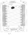
- FIG. 1is a diagrammatic view of a prior art linear infrared sensing array with infra red light source transmitters on one rail and light detecting receivers on the opposite, facing rail;
- FIG. 2is a diagram illustrating the linear resolution of the prior art sensing array of FIG. 1;
- FIG. 3is a diagrammatic view of a photoelectric sensing array apparatus, which is constructed in accordance with the present invention.
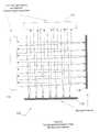
- FIG. 4is a diagram illustrating the linear resolution of the sensing array apparatus of FIG. 3 for comparison with the diagram of FIG. 2 of the prior art;
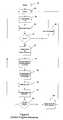
- FIG. 5is a functional block diagram of the apparatus of FIG. 3;
- FIGS. 6 and 7are flow chart diagrams of the control software of the apparatus of FIG. 3.
- FIG. 8is a diagrammatic view of another photoelectric sensing array apparatus, which is also constructed in accordance with the present invention.
- FIGS. 1 and 2there is shown a conventional infra red (IR) sensor array 1 , which is constructed in accordance with the teachings of the prior art, and which is used for position sensing.
- a row of infra red light emitting diode (LED) transmitters generally indicated at 3are mounted on a rail 4 .
- a row of light sensing receivers (photo detectors) generally indicated at 5are mounted on an opposite rail 6 .
- the position of an opaque object 7 located between the transmitters 3 and the receivers 5is determined by individually pulsing the transmitters 3 , while electronically sensing the response of the receivers 5 .
- An infra red light source printed circuit assembly 8energizes selectively the transmitters 3 to produce a group of equally spaced apart invisible light beams directed toward individual ones of the receivers, whereby corresponding ones of the receivers are blocked at the position where the opaque object 7 is located.
- An infra red light detector printed circuit assembly 9responds to each one of the receivers so that the center of the opaque object 7 can be determined by electronically sensing current flow in each one of the photo sensor receivers 5 .
- An electronic sense and control printed circuit assembly 2provides address signals to the assemblies 8 and 9 to synchronize their operations. Also, the assembly 2 responds to a blocked detector data signal for computing the center point of the region of blocked receivers in accordance with known techniques.
- a sensor arrayis a single axis system, but a two axis system for creating a two dimensional sensing grid may be employed for certain applications such as a touch screen.
- FIGS. 3 and 4there is shown a photoelectric sensing array apparatus 10 , which is constructed in accordance with the present invention.
- the linear sensing array apparatus of FIG. 3includes a pair of rails 12 and 14 , each of which includes one of a pair of rows 16 and 18 of alternating IR light emitting diode transmitters generally indicated at 21 in row 16 and at 23 in row 18 , and sensing receivers (photo detectors) generally indicated at 25 in row 16 and at 27 in row 18 .
- the right rail 12has a similar printed circuit assembly of transmitters and receivers as compared to the left rail 14 , but the rail 12 has been inverted by 180 degrees so that the transmitters of one rail are aligned with receivers of the opposite rail.
- the transmitter 21 of the rail 12is aligned with the receiver 27 of the rail 14 so that an opaque object 36 can block the light from the transmitter 21 from being received by the receiver 27 .
- both rails 12 and 14can use the same electronic printed circuit card if the LED transmitters and detector addressing lines are logically inverted on one of the rails. Thus, a cost savings for both design and manufacture is realized.
- the minimum light beam spacingis less than the diameter of the largest component. It is one-half (1 ⁇ 2) the sum of the larger component and the smaller component.
- sun sensing switches 38 or 41are triggered to provide a sunblind signal to a control assembly 34 to cause it to ignore the receivers on that side of the array and accept position data only from the opposite side.
- the switchesare positioned adjacent to the corresponding assemblies 29 and 32 . According to the invention, this cuts the effective resolution of the apparatus 10 in half during the blinded period, but enables it to remain functional.
- the photoelectric switches 38 and 41can be implemented in hardware by using directional ambient light sensors. Another method employs software pattern sensing of the existing sensor data from each side. With systems using a micro controller, pattern sensing is preferred, because it can also be used to detect and ignore faulty components. The software for pattern sensing in hereinafter described in greater detail (when software is used then the hardware switches 38 and 41 need not be used).
- the same IR source and detector assembliescan be used with mirrored surfaces to reduce overall system costs.
- the infra red light source and detector printed circuit assembly 29generally comprises light emitting diode drivers 43 for energizing selectively the infra red light source transmitters 21 of the row 16 under the control of an address select 45 which de-multiplexes the inverted address lines from the assembly 34 .
- An AND gate 47synchronizes the drivers 43 under the control of an oscillator 49 in the presence of a write enable signal from the control assembly 34 .
- a multiplexer 52receives the data from the infra red detector receivers 25 , and the output of the multiplexer 52 is amplified by a pre-amplifier 54 .
- a frequency discriminator 56 controlled by a synchronized oscillator 58generates a detect signal for the control assembly 34 .
- the assembly 32includes a light emitter diode driver 61 for selectively energizing the infra red light source transmitters 23 in a similar manner as the drivers 43 selectively energize the transmitters 21 .
- An address select 62de-multiplexes the address lines from the control assembly 34 in a similar manner as the address select 45 de-multiplexes the inverted address lines from the assembly 34 .
- An AND gate 63 and an oscillator 64synchronizes the address data supplied to the drivers 61 under the control of a write enable signal from the control assembly 34 .
- a multiplexer 65 for the infra red detector receivers 27generate a detect signal for the control assembly 34 via a pre-amplifier 66 , and a frequency discriminator 67 controlled by a synchronized oscillator 68 in a similar manner as the corresponding components of the assembly 29 .
- the assembly 34includes a processor 72 such as a suitable conventional microprocessor, for providing the address information for controlling the rail 18 and for providing inverted address information for controlling the rail 16 .
- a processor 72such as a suitable conventional microprocessor, for providing the address information for controlling the rail 18 and for providing inverted address information for controlling the rail 16 .
- An RS 232 serial port 74conveys output information from the processor 72 for position data output.
- a control program memory 76 and a data memory 78are provided for the processor 72 .
- a set of digital output latches 81are utilized for receiving and temporarily storing the address information for the assemblies 29 and 32 .
- a right and left rail digital inputs 83 and 85receive the detect signals from the respective assemblies 29 and 32 , as well as the sun blind switch information from the respective switches 38 and 41 , if employed in place of the software pattern recognition.
- the programis initiated by a startup routine as indicated at box 87 , and includes an initialization routine as indicated at 88 . Thereafter, the output address lines are selectively enabled at 89 , and then the read detect lines are accessed at 90 .
- the processor 72computes the center of the blocked detectors on the left rail 18 at 94 . Thereafter, the processor computes the center of the blocked detectors on the right rail 16 as indicated at box 95 .
- the processor 72determines the difference between the left hit count and the right hit count. The difference is then determined to be the count delta. This is indicated at box 101 . Thereafter, a decision is made at box 102 by the processor 72 as to whether or not the count delta is greater than three. If it is, then the processor 72 determines that the small count rail data should be used for both rails as indicated at 103 , and then the routine advances to a continue normal processing box 104 . If the count delta is not greater than three, then the processor 72 determines the difference between the left hit span and the right hit span as being equal to a span delta as indicated at 105 .
- the processor 72determines whether or not the span delta is greater than three as indicated at 106 . If it is greater than three, then the processor 72 determines that the larger span rail is invalid, and thus the short span rail data should be used exclusively as indicated in 107 , and thereafter the routine returns to the continue normal processing box 104 . If the span delta is not greater than three, then the program advances directly to the continue normal processing box 104 .
- FIG. 8there is shown another photoelectric sensing arrangement apparatus 109 , which is also constructed in accordance with the present invention, and which is similar to the apparatus 10 except that the apparatus 109 is a two dimensional sensor array utilizing reflective surfaces to reflect the beams from transmitters to receivers.
- the apparatus 109includes top and left hand infra red light source and detector printed circuit assemblies 112 and 114 , which are positioned at right angles to one another, and which are similar in construction to the assemblies 29 and 32 .
- a bottom mirrored surface 116receives the infra red light beams from the assembly 112 and reflects them back to the assembly 112 .
- a right mirrored surface 118is disposed oppositely to the assembly 114 and reflects the infra red beams from the assembly 104 back thereto. In this manner, there are both vertical and horizontal sensing axes to provide a two dimensional sensor array.
Landscapes
- Engineering & Computer Science (AREA)
- Physics & Mathematics (AREA)
- General Physics & Mathematics (AREA)
- General Engineering & Computer Science (AREA)
- Theoretical Computer Science (AREA)
- Life Sciences & Earth Sciences (AREA)
- General Life Sciences & Earth Sciences (AREA)
- Geophysics (AREA)
- Human Computer Interaction (AREA)
- Geophysics And Detection Of Objects (AREA)
- Switches Operated By Changes In Physical Conditions (AREA)
- Length Measuring Devices By Optical Means (AREA)
Abstract
Description
Claims (9)
Priority Applications (4)
| Application Number | Priority Date | Filing Date | Title |
|---|---|---|---|
| US09/528,789US6495832B1 (en) | 2000-03-15 | 2000-03-15 | Photoelectric sensing array apparatus and method of using same |
| PCT/US2001/007903WO2001069582A1 (en) | 2000-03-15 | 2001-03-12 | Photoelectric sensing array apparatus and method of using same |
| EP01920314AEP1266372A1 (en) | 2000-03-15 | 2001-03-12 | Photoelectric sensing array apparatus and method of using same |
| CA002403216ACA2403216A1 (en) | 2000-03-15 | 2001-03-12 | Photoelectric sensing array apparatus and method of using same |
Applications Claiming Priority (1)
| Application Number | Priority Date | Filing Date | Title |
|---|---|---|---|
| US09/528,789US6495832B1 (en) | 2000-03-15 | 2000-03-15 | Photoelectric sensing array apparatus and method of using same |
Publications (1)
| Publication Number | Publication Date |
|---|---|
| US6495832B1true US6495832B1 (en) | 2002-12-17 |
Family
ID=24107189
Family Applications (1)
| Application Number | Title | Priority Date | Filing Date |
|---|---|---|---|
| US09/528,789Expired - Fee RelatedUS6495832B1 (en) | 2000-03-15 | 2000-03-15 | Photoelectric sensing array apparatus and method of using same |
Country Status (4)
| Country | Link |
|---|---|
| US (1) | US6495832B1 (en) |
| EP (1) | EP1266372A1 (en) |
| CA (1) | CA2403216A1 (en) |
| WO (1) | WO2001069582A1 (en) |
Cited By (52)
| Publication number | Priority date | Publication date | Assignee | Title |
|---|---|---|---|---|
| US20040078102A1 (en)* | 2002-10-17 | 2004-04-22 | Lopez Matthew G | Light responsive data entry system |
| US20040144914A1 (en)* | 2001-08-28 | 2004-07-29 | Leopold Kostal Gmbh & Co. Kg | Device for the optoelectronic detection of switching positions of a switching element |
| WO2005114263A1 (en)* | 2004-05-19 | 2005-12-01 | Daimlerchrysler Ag | Device and method for identifying an object in or on a closable opening |
| GB2421304A (en)* | 2004-12-16 | 2006-06-21 | Agilent Technologies Inc | Optical touch panel with integrated arrays of opposing alternating emitters and detectors |
| US20060202974A1 (en)* | 2005-03-10 | 2006-09-14 | Jeffrey Thielman | Surface |
| US20060226797A1 (en)* | 2003-12-16 | 2006-10-12 | Leopold Kostal Gmbh & Co. Kg | Steering column switch system comprising an emergency operation function |
| US20070211037A1 (en)* | 2006-03-09 | 2007-09-13 | Sun Brian Y | Photoelectric sensing array apparatus |
| US20080136780A1 (en)* | 2006-12-07 | 2008-06-12 | Yuan-Jung Chang | Method for generating a laser light detecting signal of an optical mouse |
| US7421167B2 (en) | 2004-12-09 | 2008-09-02 | Rpo Pty Limited | Optical power distribution devices |
| US20100245117A1 (en)* | 2007-11-07 | 2010-09-30 | Cedes Ag | System for detecting an object in a monitoring area |
| US20110157096A1 (en)* | 2008-08-07 | 2011-06-30 | Owen Drumm | Method and Apparatus For Detecting A Multitouch Event In An Optical Touch-Sensitive Device |
| US20120176345A1 (en)* | 2009-09-30 | 2012-07-12 | Beijing Irtouch Systems Co., Ltd. | Touch screen, touch system and method for positioning a touch object in touch system |
| US20120218230A1 (en)* | 2009-11-05 | 2012-08-30 | Shanghai Jingyan Electronic Technology Co., Ltd. | Infrared touch screen device and multipoint locating method thereof |
| JP2014032965A (en)* | 2013-10-11 | 2014-02-20 | Keyence Corp | Multi-optical axis photoelectric sensor |
| US20140152539A1 (en)* | 2012-12-03 | 2014-06-05 | Qualcomm Incorporated | Apparatus and method for an infrared contactless gesture system |
| US20140210470A1 (en)* | 2013-01-31 | 2014-07-31 | Ge Medical Systems Global Technology Company, Llc | Automatic detection of patient body profile and intelligent positioning of patient |
| KR101466737B1 (en)* | 2012-02-07 | 2014-11-28 | 주식회사 비즈모델라인 | Frame units for tank marksmanship training target frame |
| KR101466733B1 (en)* | 2012-01-10 | 2014-12-02 | 주식회사 비즈모델라인 | Target system of tank marksmanship training |
| US9052778B2 (en)* | 2009-12-16 | 2015-06-09 | Beijing Irtouch Systems Co., Ltd | Infrared touch screen |
| US9098144B1 (en) | 2011-12-05 | 2015-08-04 | Cypress Semiconductor Corporation | Adaptive ambient light auto-movement blocking in optical navigation modules |
| US20150242055A1 (en)* | 2012-05-23 | 2015-08-27 | Flatfrog Laboratories Ab | Touch-sensitive apparatus with improved spatial resolution |
| US9170683B2 (en) | 2011-07-22 | 2015-10-27 | Rapt Ip Limited | Optical coupler for use in an optical touch sensitive device |
| US9552104B2 (en) | 2008-08-07 | 2017-01-24 | Rapt Ip Limited | Detecting multitouch events in an optical touch-sensitive device using touch event templates |
| US9874978B2 (en) | 2013-07-12 | 2018-01-23 | Flatfrog Laboratories Ab | Partial detect mode |
| TWI616794B (en)* | 2016-12-20 | 2018-03-01 | 友達光電股份有限公司 | Photo sensing circuit and defect curing method thereof |
| US9916041B2 (en) | 2012-07-13 | 2018-03-13 | Rapt Ip Limited | Low power operation of an optical touch-sensitive device for detecting multitouch events |
| US10019113B2 (en) | 2013-04-11 | 2018-07-10 | Flatfrog Laboratories Ab | Tomographic processing for touch detection |
| US10126882B2 (en) | 2014-01-16 | 2018-11-13 | Flatfrog Laboratories Ab | TIR-based optical touch systems of projection-type |
| US10146376B2 (en) | 2014-01-16 | 2018-12-04 | Flatfrog Laboratories Ab | Light coupling in TIR-based optical touch systems |
| US10161886B2 (en) | 2014-06-27 | 2018-12-25 | Flatfrog Laboratories Ab | Detection of surface contamination |
| US10168835B2 (en) | 2012-05-23 | 2019-01-01 | Flatfrog Laboratories Ab | Spatial resolution in touch displays |
| US10282035B2 (en) | 2016-12-07 | 2019-05-07 | Flatfrog Laboratories Ab | Touch device |
| US10318074B2 (en) | 2015-01-30 | 2019-06-11 | Flatfrog Laboratories Ab | Touch-sensing OLED display with tilted emitters |
| US10401546B2 (en) | 2015-03-02 | 2019-09-03 | Flatfrog Laboratories Ab | Optical component for light coupling |
| US10437389B2 (en) | 2017-03-28 | 2019-10-08 | Flatfrog Laboratories Ab | Touch sensing apparatus and method for assembly |
| US10474249B2 (en) | 2008-12-05 | 2019-11-12 | Flatfrog Laboratories Ab | Touch sensing apparatus and method of operating the same |
| US10481737B2 (en) | 2017-03-22 | 2019-11-19 | Flatfrog Laboratories Ab | Pen differentiation for touch display |
| US10496227B2 (en) | 2015-02-09 | 2019-12-03 | Flatfrog Laboratories Ab | Optical touch system comprising means for projecting and detecting light beams above and inside a transmissive panel |
| DE102005013352B4 (en)* | 2005-03-23 | 2020-07-09 | Mechaless Systems Gmbh | Device and method for recognizing an object in or on a closable opening |
| US10761657B2 (en) | 2016-11-24 | 2020-09-01 | Flatfrog Laboratories Ab | Automatic optimisation of touch signal |
| US11182023B2 (en) | 2015-01-28 | 2021-11-23 | Flatfrog Laboratories Ab | Dynamic touch quarantine frames |
| US11256371B2 (en) | 2017-09-01 | 2022-02-22 | Flatfrog Laboratories Ab | Optical component |
| US11301089B2 (en) | 2015-12-09 | 2022-04-12 | Flatfrog Laboratories Ab | Stylus identification |
| WO2022198933A1 (en)* | 2021-03-25 | 2022-09-29 | 无锡德芯微电子有限公司 | Photoelectric detection system based on power source coding, and control method and coding method |
| US11474644B2 (en) | 2017-02-06 | 2022-10-18 | Flatfrog Laboratories Ab | Optical coupling in touch-sensing systems |
| US11567610B2 (en) | 2018-03-05 | 2023-01-31 | Flatfrog Laboratories Ab | Detection line broadening |
| CN115876041A (en)* | 2023-01-12 | 2023-03-31 | 西安工业大学 | Supersonic velocity target outer trajectory parameter measuring device and measuring method |
| US11893189B2 (en) | 2020-02-10 | 2024-02-06 | Flatfrog Laboratories Ab | Touch-sensing apparatus |
| US11943563B2 (en) | 2019-01-25 | 2024-03-26 | FlatFrog Laboratories, AB | Videoconferencing terminal and method of operating the same |
| US12055969B2 (en) | 2018-10-20 | 2024-08-06 | Flatfrog Laboratories Ab | Frame for a touch-sensitive device and tool therefor |
| US12056316B2 (en) | 2019-11-25 | 2024-08-06 | Flatfrog Laboratories Ab | Touch-sensing apparatus |
| US12282653B2 (en) | 2020-02-08 | 2025-04-22 | Flatfrog Laboratories Ab | Touch apparatus with low latency interactions |
Families Citing this family (7)
| Publication number | Priority date | Publication date | Assignee | Title |
|---|---|---|---|---|
| US6927384B2 (en) | 2001-08-13 | 2005-08-09 | Nokia Mobile Phones Ltd. | Method and device for detecting touch pad unit |
| EP1870734B1 (en)* | 2006-06-20 | 2009-01-14 | Sick Ag | Opto-electronic light curtain with at least two transmitting-receiving bars |
| DE102007024210A1 (en)* | 2007-05-15 | 2008-11-27 | Pilz Gmbh & Co. Kg | Optoelectronic sensor to protect a hazardous area |
| KR101009278B1 (en)* | 2008-10-02 | 2011-01-18 | 한국과학기술연구원 | Optical recognition user input device and user input recognition method |
| DE102010061194A1 (en)* | 2010-12-13 | 2012-06-14 | Sick Ag | Optoelectronic sensor |
| EP2808706B1 (en) | 2013-05-28 | 2023-06-28 | Rockwell Automation Switzerland GmbH | Transceiver element for an optical unit of a photoelectric barrier and photoelectric light curtain |
| CN109654953B (en)* | 2018-12-18 | 2021-06-29 | 南京理工大学 | A method for measuring target coordinates and velocity of projectile with large target surface |
Citations (8)
| Publication number | Priority date | Publication date | Assignee | Title |
|---|---|---|---|---|
| US4672364A (en)* | 1984-06-18 | 1987-06-09 | Carroll Touch Inc | Touch input device having power profiling |
| US4891508A (en) | 1988-06-30 | 1990-01-02 | Hewlett-Packard Company | Precision infrared position detector apparatus for touch screen system |
| US4893120A (en) | 1986-11-26 | 1990-01-09 | Digital Electronics Corporation | Touch panel using modulated light |
| US4904857A (en) | 1986-01-13 | 1990-02-27 | Nippondenso Co., Ltd. | Electric control system for photoelectric touch input apparatus |
| US4928094A (en) | 1988-01-25 | 1990-05-22 | The Boeing Company | Battery-operated data collection apparatus having an infrared touch screen data entry device |
| US5162783A (en) | 1990-07-23 | 1992-11-10 | Akzo N.V. | Infrared touch screen device for a video monitor |
| US5579035A (en) | 1991-07-05 | 1996-11-26 | Technomarket, L.P. | Liquid crystal display module |
| US5988645A (en)* | 1994-04-08 | 1999-11-23 | Downing; Dennis L. | Moving object monitoring system |
- 2000
- 2000-03-15USUS09/528,789patent/US6495832B1/ennot_activeExpired - Fee Related
- 2001
- 2001-03-12WOPCT/US2001/007903patent/WO2001069582A1/ennot_activeApplication Discontinuation
- 2001-03-12EPEP01920314Apatent/EP1266372A1/ennot_activeWithdrawn
- 2001-03-12CACA002403216Apatent/CA2403216A1/ennot_activeAbandoned
Patent Citations (8)
| Publication number | Priority date | Publication date | Assignee | Title |
|---|---|---|---|---|
| US4672364A (en)* | 1984-06-18 | 1987-06-09 | Carroll Touch Inc | Touch input device having power profiling |
| US4904857A (en) | 1986-01-13 | 1990-02-27 | Nippondenso Co., Ltd. | Electric control system for photoelectric touch input apparatus |
| US4893120A (en) | 1986-11-26 | 1990-01-09 | Digital Electronics Corporation | Touch panel using modulated light |
| US4928094A (en) | 1988-01-25 | 1990-05-22 | The Boeing Company | Battery-operated data collection apparatus having an infrared touch screen data entry device |
| US4891508A (en) | 1988-06-30 | 1990-01-02 | Hewlett-Packard Company | Precision infrared position detector apparatus for touch screen system |
| US5162783A (en) | 1990-07-23 | 1992-11-10 | Akzo N.V. | Infrared touch screen device for a video monitor |
| US5579035A (en) | 1991-07-05 | 1996-11-26 | Technomarket, L.P. | Liquid crystal display module |
| US5988645A (en)* | 1994-04-08 | 1999-11-23 | Downing; Dennis L. | Moving object monitoring system |
Cited By (85)
| Publication number | Priority date | Publication date | Assignee | Title |
|---|---|---|---|---|
| US20040144914A1 (en)* | 2001-08-28 | 2004-07-29 | Leopold Kostal Gmbh & Co. Kg | Device for the optoelectronic detection of switching positions of a switching element |
| US6800839B2 (en)* | 2001-08-28 | 2004-10-05 | Leopold Kostal Gmbh & Co. Kg | Device for the optoelectronic detection of switching positions of a switching element |
| US6904326B2 (en)* | 2002-10-17 | 2005-06-07 | Hewlett-Packard Development Company, Lp. | Light responsive data entry system |
| US20040078102A1 (en)* | 2002-10-17 | 2004-04-22 | Lopez Matthew G | Light responsive data entry system |
| US20060226797A1 (en)* | 2003-12-16 | 2006-10-12 | Leopold Kostal Gmbh & Co. Kg | Steering column switch system comprising an emergency operation function |
| CN100483076C (en)* | 2003-12-16 | 2009-04-29 | 莱奥泼德·科世达责任有限股份公司 | Steering column switch system comprising an emergency operation function |
| US7257473B2 (en)* | 2003-12-16 | 2007-08-14 | Leopold Kostal Gmbh & Co. Kg | Steering column switch system comprising an emergency operation function |
| WO2005114263A1 (en)* | 2004-05-19 | 2005-12-01 | Daimlerchrysler Ag | Device and method for identifying an object in or on a closable opening |
| US7378641B2 (en) | 2004-05-19 | 2008-05-27 | Daimler Chrysler Ag | Device and method for identifying an object in or on a closable opening |
| US7421167B2 (en) | 2004-12-09 | 2008-09-02 | Rpo Pty Limited | Optical power distribution devices |
| US20060132454A1 (en)* | 2004-12-16 | 2006-06-22 | Deng-Peng Chen | Systems and methods for high resolution optical touch position systems |
| GB2421304A (en)* | 2004-12-16 | 2006-06-21 | Agilent Technologies Inc | Optical touch panel with integrated arrays of opposing alternating emitters and detectors |
| GB2421304B (en)* | 2004-12-16 | 2009-07-08 | Agilent Technologies Inc | Touch position system and method |
| US20060202974A1 (en)* | 2005-03-10 | 2006-09-14 | Jeffrey Thielman | Surface |
| DE102005013352B4 (en)* | 2005-03-23 | 2020-07-09 | Mechaless Systems Gmbh | Device and method for recognizing an object in or on a closable opening |
| US20070211037A1 (en)* | 2006-03-09 | 2007-09-13 | Sun Brian Y | Photoelectric sensing array apparatus |
| US20080136780A1 (en)* | 2006-12-07 | 2008-06-12 | Yuan-Jung Chang | Method for generating a laser light detecting signal of an optical mouse |
| US20100245117A1 (en)* | 2007-11-07 | 2010-09-30 | Cedes Ag | System for detecting an object in a monitoring area |
| US20110157096A1 (en)* | 2008-08-07 | 2011-06-30 | Owen Drumm | Method and Apparatus For Detecting A Multitouch Event In An Optical Touch-Sensitive Device |
| US10067609B2 (en) | 2008-08-07 | 2018-09-04 | Rapt Ip Limited | Detecting multitouch events in an optical touch-sensitive device using touch event templates |
| US8350831B2 (en) | 2008-08-07 | 2013-01-08 | Rapt Ip Limited | Method and apparatus for detecting a multitouch event in an optical touch-sensitive device |
| US9335864B2 (en) | 2008-08-07 | 2016-05-10 | Rapt Ip Limited | Method and apparatus for detecting a multitouch event in an optical touch-sensitive device |
| US9552104B2 (en) | 2008-08-07 | 2017-01-24 | Rapt Ip Limited | Detecting multitouch events in an optical touch-sensitive device using touch event templates |
| US10474249B2 (en) | 2008-12-05 | 2019-11-12 | Flatfrog Laboratories Ab | Touch sensing apparatus and method of operating the same |
| US20120176345A1 (en)* | 2009-09-30 | 2012-07-12 | Beijing Irtouch Systems Co., Ltd. | Touch screen, touch system and method for positioning a touch object in touch system |
| US8928608B2 (en)* | 2009-09-30 | 2015-01-06 | Beijing Irtouch Systems Co., Ltd | Touch screen, touch system and method for positioning a touch object in touch system |
| US20120218230A1 (en)* | 2009-11-05 | 2012-08-30 | Shanghai Jingyan Electronic Technology Co., Ltd. | Infrared touch screen device and multipoint locating method thereof |
| US9052778B2 (en)* | 2009-12-16 | 2015-06-09 | Beijing Irtouch Systems Co., Ltd | Infrared touch screen |
| US9170683B2 (en) | 2011-07-22 | 2015-10-27 | Rapt Ip Limited | Optical coupler for use in an optical touch sensitive device |
| US9098144B1 (en) | 2011-12-05 | 2015-08-04 | Cypress Semiconductor Corporation | Adaptive ambient light auto-movement blocking in optical navigation modules |
| KR101466733B1 (en)* | 2012-01-10 | 2014-12-02 | 주식회사 비즈모델라인 | Target system of tank marksmanship training |
| KR101466737B1 (en)* | 2012-02-07 | 2014-11-28 | 주식회사 비즈모델라인 | Frame units for tank marksmanship training target frame |
| US20150242055A1 (en)* | 2012-05-23 | 2015-08-27 | Flatfrog Laboratories Ab | Touch-sensitive apparatus with improved spatial resolution |
| US10168835B2 (en) | 2012-05-23 | 2019-01-01 | Flatfrog Laboratories Ab | Spatial resolution in touch displays |
| US9916041B2 (en) | 2012-07-13 | 2018-03-13 | Rapt Ip Limited | Low power operation of an optical touch-sensitive device for detecting multitouch events |
| US20140152539A1 (en)* | 2012-12-03 | 2014-06-05 | Qualcomm Incorporated | Apparatus and method for an infrared contactless gesture system |
| US9977503B2 (en)* | 2012-12-03 | 2018-05-22 | Qualcomm Incorporated | Apparatus and method for an infrared contactless gesture system |
| CN103961133B (en)* | 2013-01-31 | 2018-09-11 | Ge医疗系统环球技术有限公司 | Automatic detection of patient body shape and intelligent patient positioning |
| US20140210470A1 (en)* | 2013-01-31 | 2014-07-31 | Ge Medical Systems Global Technology Company, Llc | Automatic detection of patient body profile and intelligent positioning of patient |
| CN108324311A (en)* | 2013-01-31 | 2018-07-27 | Ge医疗系统环球技术有限公司 | Patient body shape detects automatically and patient's intelligent positioning |
| US9610049B2 (en)* | 2013-01-31 | 2017-04-04 | General Electric Company | Automatic detection of patient body profile and intelligent positioning of patient |
| CN103961133A (en)* | 2013-01-31 | 2014-08-06 | Ge医疗系统环球技术有限公司 | Automatic detection of patient body shape and intelligent patient positioning |
| US10019113B2 (en) | 2013-04-11 | 2018-07-10 | Flatfrog Laboratories Ab | Tomographic processing for touch detection |
| US9874978B2 (en) | 2013-07-12 | 2018-01-23 | Flatfrog Laboratories Ab | Partial detect mode |
| JP2014032965A (en)* | 2013-10-11 | 2014-02-20 | Keyence Corp | Multi-optical axis photoelectric sensor |
| US10126882B2 (en) | 2014-01-16 | 2018-11-13 | Flatfrog Laboratories Ab | TIR-based optical touch systems of projection-type |
| US10146376B2 (en) | 2014-01-16 | 2018-12-04 | Flatfrog Laboratories Ab | Light coupling in TIR-based optical touch systems |
| US10161886B2 (en) | 2014-06-27 | 2018-12-25 | Flatfrog Laboratories Ab | Detection of surface contamination |
| US11182023B2 (en) | 2015-01-28 | 2021-11-23 | Flatfrog Laboratories Ab | Dynamic touch quarantine frames |
| US10318074B2 (en) | 2015-01-30 | 2019-06-11 | Flatfrog Laboratories Ab | Touch-sensing OLED display with tilted emitters |
| US10496227B2 (en) | 2015-02-09 | 2019-12-03 | Flatfrog Laboratories Ab | Optical touch system comprising means for projecting and detecting light beams above and inside a transmissive panel |
| US11029783B2 (en) | 2015-02-09 | 2021-06-08 | Flatfrog Laboratories Ab | Optical touch system comprising means for projecting and detecting light beams above and inside a transmissive panel |
| US10401546B2 (en) | 2015-03-02 | 2019-09-03 | Flatfrog Laboratories Ab | Optical component for light coupling |
| US11301089B2 (en) | 2015-12-09 | 2022-04-12 | Flatfrog Laboratories Ab | Stylus identification |
| US10761657B2 (en) | 2016-11-24 | 2020-09-01 | Flatfrog Laboratories Ab | Automatic optimisation of touch signal |
| US12189906B2 (en) | 2016-12-07 | 2025-01-07 | Flatfrog Laboratories Ab | Touch device |
| US11579731B2 (en) | 2016-12-07 | 2023-02-14 | Flatfrog Laboratories Ab | Touch device |
| US11281335B2 (en) | 2016-12-07 | 2022-03-22 | Flatfrog Laboratories Ab | Touch device |
| US10775935B2 (en) | 2016-12-07 | 2020-09-15 | Flatfrog Laboratories Ab | Touch device |
| US10282035B2 (en) | 2016-12-07 | 2019-05-07 | Flatfrog Laboratories Ab | Touch device |
| TWI616794B (en)* | 2016-12-20 | 2018-03-01 | 友達光電股份有限公司 | Photo sensing circuit and defect curing method thereof |
| US11474644B2 (en) | 2017-02-06 | 2022-10-18 | Flatfrog Laboratories Ab | Optical coupling in touch-sensing systems |
| US11740741B2 (en) | 2017-02-06 | 2023-08-29 | Flatfrog Laboratories Ab | Optical coupling in touch-sensing systems |
| US12175044B2 (en) | 2017-02-06 | 2024-12-24 | Flatfrog Laboratories Ab | Optical coupling in touch-sensing systems |
| US10606414B2 (en) | 2017-03-22 | 2020-03-31 | Flatfrog Laboratories Ab | Eraser for touch displays |
| US11099688B2 (en) | 2017-03-22 | 2021-08-24 | Flatfrog Laboratories Ab | Eraser for touch displays |
| US10481737B2 (en) | 2017-03-22 | 2019-11-19 | Flatfrog Laboratories Ab | Pen differentiation for touch display |
| US11016605B2 (en) | 2017-03-22 | 2021-05-25 | Flatfrog Laboratories Ab | Pen differentiation for touch displays |
| US10606416B2 (en) | 2017-03-28 | 2020-03-31 | Flatfrog Laboratories Ab | Touch sensing apparatus and method for assembly |
| US10739916B2 (en) | 2017-03-28 | 2020-08-11 | Flatfrog Laboratories Ab | Touch sensing apparatus and method for assembly |
| US10437389B2 (en) | 2017-03-28 | 2019-10-08 | Flatfrog Laboratories Ab | Touch sensing apparatus and method for assembly |
| US11281338B2 (en) | 2017-03-28 | 2022-03-22 | Flatfrog Laboratories Ab | Touch sensing apparatus and method for assembly |
| US11269460B2 (en) | 2017-03-28 | 2022-03-08 | Flatfrog Laboratories Ab | Touch sensing apparatus and method for assembly |
| US10845923B2 (en) | 2017-03-28 | 2020-11-24 | Flatfrog Laboratories Ab | Touch sensing apparatus and method for assembly |
| US12086362B2 (en) | 2017-09-01 | 2024-09-10 | Flatfrog Laboratories Ab | Optical component |
| US11256371B2 (en) | 2017-09-01 | 2022-02-22 | Flatfrog Laboratories Ab | Optical component |
| US11650699B2 (en) | 2017-09-01 | 2023-05-16 | Flatfrog Laboratories Ab | Optical component |
| US11567610B2 (en) | 2018-03-05 | 2023-01-31 | Flatfrog Laboratories Ab | Detection line broadening |
| US12055969B2 (en) | 2018-10-20 | 2024-08-06 | Flatfrog Laboratories Ab | Frame for a touch-sensitive device and tool therefor |
| US11943563B2 (en) | 2019-01-25 | 2024-03-26 | FlatFrog Laboratories, AB | Videoconferencing terminal and method of operating the same |
| US12056316B2 (en) | 2019-11-25 | 2024-08-06 | Flatfrog Laboratories Ab | Touch-sensing apparatus |
| US12282653B2 (en) | 2020-02-08 | 2025-04-22 | Flatfrog Laboratories Ab | Touch apparatus with low latency interactions |
| US11893189B2 (en) | 2020-02-10 | 2024-02-06 | Flatfrog Laboratories Ab | Touch-sensing apparatus |
| WO2022198933A1 (en)* | 2021-03-25 | 2022-09-29 | 无锡德芯微电子有限公司 | Photoelectric detection system based on power source coding, and control method and coding method |
| CN115876041A (en)* | 2023-01-12 | 2023-03-31 | 西安工业大学 | Supersonic velocity target outer trajectory parameter measuring device and measuring method |
Also Published As
| Publication number | Publication date |
|---|---|
| CA2403216A1 (en) | 2001-09-20 |
| EP1266372A1 (en) | 2002-12-18 |
| WO2001069582A1 (en) | 2001-09-20 |
Similar Documents
| Publication | Publication Date | Title |
|---|---|---|
| US6495832B1 (en) | Photoelectric sensing array apparatus and method of using same | |
| US5355222A (en) | Optical receiver for area location system | |
| US6677934B1 (en) | Infrared touch panel with improved sunlight rejection | |
| CN103518184B (en) | Use the optical touch screen of total internal reflection | |
| USRE33668E (en) | Detection device having energy transmitters located at vertically spaced apart points along movable doors | |
| US6229529B1 (en) | Write point detecting circuit to detect multiple write points | |
| KR100829172B1 (en) | Coordinate calculation method of touch point of infrared touch screen device and infrared touch screen | |
| EP0601651A1 (en) | Optical touch tablet based on sector cross bearing | |
| WO1990015966A1 (en) | Optical tablet construction | |
| CN101930306A (en) | Multi-touch device and detection method thereof | |
| US8164581B2 (en) | Optical touch module | |
| EP0070883B1 (en) | Photoelectric obstruction detector for elevator doorways | |
| GB2214635A (en) | Optical input device | |
| CN100334439C (en) | Reflective sensor, filtering plate and detecting method for detected objects | |
| CN107782354B (en) | Motion sensor detection system and method | |
| JP2017190967A (en) | Human body detection system and human body detection method | |
| US20070241262A1 (en) | Optical sensing unit for an optical input device | |
| US20120176592A1 (en) | Optical sensor | |
| US20010020685A1 (en) | Detector and method for detecting plate-shaped or sheet-shaped body | |
| JPH0612512B2 (en) | Optical touch panel light receiving element sensitivity adjustment method | |
| JP2005181116A (en) | Infrared sensor device | |
| JP2529094B2 (en) | Object position sensor | |
| JPS5830637B2 (en) | distributed smoke detector | |
| JPH054035Y2 (en) | ||
| JP2752679B2 (en) | Human body detection device |
Legal Events
| Date | Code | Title | Description |
|---|---|---|---|
| AS | Assignment | Owner name:TOUCH CONTROLS, INC., CALIFORNIA Free format text:ASSIGNMENT OF ASSIGNORS INTEREST;ASSIGNOR:KIRBY, JOSEPH J.;REEL/FRAME:011131/0643 Effective date:20000315 | |
| FEPP | Fee payment procedure | Free format text:PAT HOLDER NO LONGER CLAIMS SMALL ENTITY STATUS, ENTITY STATUS SET TO UNDISCOUNTED (ORIGINAL EVENT CODE: STOL); ENTITY STATUS OF PATENT OWNER: LARGE ENTITY | |
| REMI | Maintenance fee reminder mailed | ||
| REIN | Reinstatement after maintenance fee payment confirmed | ||
| FP | Lapsed due to failure to pay maintenance fee | Effective date:20061217 | |
| FEPP | Fee payment procedure | Free format text:PETITION RELATED TO MAINTENANCE FEES FILED (ORIGINAL EVENT CODE: PMFP); ENTITY STATUS OF PATENT OWNER: LARGE ENTITY | |
| FEPP | Fee payment procedure | Free format text:PETITION RELATED TO MAINTENANCE FEES GRANTED (ORIGINAL EVENT CODE: PMFG); ENTITY STATUS OF PATENT OWNER: LARGE ENTITY | |
| AS | Assignment | Owner name:KONTRON AMERICA, INCORPORATED, CALIFORNIA Free format text:CHANGE OF NAME;ASSIGNOR:TOUCH CONTROLS, INC.;REEL/FRAME:020645/0704 Effective date:20051214 Owner name:AZONIX CORPORATION, MASSACHUSETTS Free format text:ASSIGNMENT OF ASSIGNORS INTEREST;ASSIGNOR:KONTRON AMERICA, INC.;REEL/FRAME:020645/0711 Effective date:20070813 | |
| FPAY | Fee payment | Year of fee payment:4 | |
| SULP | Surcharge for late payment | ||
| PRDP | Patent reinstated due to the acceptance of a late maintenance fee | Effective date:20080516 | |
| REMI | Maintenance fee reminder mailed | ||
| LAPS | Lapse for failure to pay maintenance fees | ||
| STCH | Information on status: patent discontinuation | Free format text:PATENT EXPIRED DUE TO NONPAYMENT OF MAINTENANCE FEES UNDER 37 CFR 1.362 | |
| FP | Lapsed due to failure to pay maintenance fee | Effective date:20101217 |