US6493795B1 - Data storage system - Google Patents
Data storage systemDownload PDFInfo
- Publication number
- US6493795B1 US6493795B1US09/223,417US22341798AUS6493795B1US 6493795 B1US6493795 B1US 6493795B1US 22341798 AUS22341798 AUS 22341798AUS 6493795 B1US6493795 B1US 6493795B1
- Authority
- US
- United States
- Prior art keywords
- dual
- data
- pair
- memory
- write
- Prior art date
- Legal status (The legal status is an assumption and is not a legal conclusion. Google has not performed a legal analysis and makes no representation as to the accuracy of the status listed.)
- Expired - Lifetime
Links
Images


Classifications
- G—PHYSICS
- G06—COMPUTING OR CALCULATING; COUNTING
- G06F—ELECTRIC DIGITAL DATA PROCESSING
- G06F13/00—Interconnection of, or transfer of information or other signals between, memories, input/output devices or central processing units
- G06F13/10—Program control for peripheral devices
- G06F13/12—Program control for peripheral devices using hardware independent of the central processor, e.g. channel or peripheral processor
- G—PHYSICS
- G06—COMPUTING OR CALCULATING; COUNTING
- G06F—ELECTRIC DIGITAL DATA PROCESSING
- G06F11/00—Error detection; Error correction; Monitoring
- G06F11/07—Responding to the occurrence of a fault, e.g. fault tolerance
- G06F11/16—Error detection or correction of the data by redundancy in hardware
- G06F11/20—Error detection or correction of the data by redundancy in hardware using active fault-masking, e.g. by switching out faulty elements or by switching in spare elements
- G06F11/2053—Error detection or correction of the data by redundancy in hardware using active fault-masking, e.g. by switching out faulty elements or by switching in spare elements where persistent mass storage functionality or persistent mass storage control functionality is redundant
- G06F11/2056—Error detection or correction of the data by redundancy in hardware using active fault-masking, e.g. by switching out faulty elements or by switching in spare elements where persistent mass storage functionality or persistent mass storage control functionality is redundant by mirroring
- G06F11/2087—Error detection or correction of the data by redundancy in hardware using active fault-masking, e.g. by switching out faulty elements or by switching in spare elements where persistent mass storage functionality or persistent mass storage control functionality is redundant by mirroring with a common controller
Definitions
- This inventionrelates generally to data storage systems, and more particularly to data storage systems having redundancy arrangements to protect against total system failure in the event of a failure in a component or subassembly of the storage system.
- large mainframe computer systemsrequire large capacity data storage systems.
- These large main frame computer systemsgenerally includes data processors which perform many operations on data introduced to the computer system through peripherals including the data storage system. The results of these operations are output to peripherals, including the storage system.
- One type of data storage systemis a magnetic disk storage system.
- a bank of disk drives and the main frame computer systemare coupled together through an interface.
- the interfaceincludes CPU, or “front end”, controllers (or directors) and “back end” disk controllers (or directors).
- the interfaceoperates the controllers (or directors) in such a way that they are transparent to the computer. That is, data is stored in, and retrieved from, the bank of disk drives in such a way that the mainframe computer system merely thinks it is operating with one mainframe memory.
- One such systemis described in U.S. Pat. No. 5,206,939, entitled “System and Method for Disk Mapping and Data Retrieval”, inventors Moshe Yanai, Natan Vishlitzky, Bruno Alterescu and Daniel Castel, issued Apr. 27, 1993, and assigned to the same assignee as the present invention.
- the interfacemay also include, in addition to the CPU controllers (or directors) and disk controllers (or directors), addressable cache memories.
- the cache memoryis a semiconductor memory and is provided to rapidly store data from the main frame computer system before storage in the disk drives, and, on the other hand, store data from the disk drives prior to being sent to the main frame computer.
- the cache memorybeing a semiconductor memory, as distinguished from a magnetic memory as in the case of the disk drives, is much faster than the disk drives in reading and writing data.
- the CPU controllers, disk controllers and cache memoryare interconnected through a backplane printed circuit board. More particularly, disk controllers are mounted on disk controller printed circuit boards. CPU controllers are mounted on CPU controller printed circuit boards. And, cache memories are mounted on cache memory printed circuit boards. The disk controller, CPU controller and cache memory printed circuit boards plug into the backplane printed circuit board. In order to provide data integrity in case of a failure in a controller, the backplane printed circuit board has a system bus made up of a pair of buses. One set the disk controllers is connected to one bus and another set of the disk controllers is connected to the other bus. Likewise, one set the CPU controllers is connected to one bus and another set of the CPU controllers is connected to the other bus. The cache memories are connected to both buses. Each one of the buses provides data, address and control information.
- the use of two busesprovides a degree of redundancy to protect against a total system failure in the event that the controllers, or disk drives connected to one bus fail. Further, the use of two buses increases the data transfer bandwidth of the system compared to a system having a single bus.
- a data storage systemwherein a host computer is coupled to a bank of disk drives through an interface.
- the interfaceincludes a system memory comprising a pair of system memory sections. Each one of the memory sections has a plurality of addressable locations for storing data written into such one of the memory sections at the addressable locations.
- a system busis coupled to the pair of system memory sections.
- a plurality of directorsis coupled to the system memory through the system bus, such directors being configured to control data transfer between the host computer and the bank of disk drives as such data passes through the system memory.
- the directorsare configured to place the system in a dual-write mode, and in such mode, store therein a burst of the data to be transferred between the host computer and the bank of disk drives, transfer such stored burst of data sequentially to the system bus, and enable both of the memory sections coupled to such system bus to have written therein, at the same one of the addressable locations, the same burst of data transferred sequentially to the system bus.
- the interfaceincludes a system memory having a pair of system memory sections. Each one of the system memory sections has a plurality of addressable locations for storing data written into such one of the memory sections at the addressable locations.
- a system buscomprising a pair of system busses is provided, each one of the pair of system busses being coupled to a corresponding one of the pair of system memory sections.
- a plurality of directorsis coupled to the system memory through the system bus. The directors are configured to control data transfer between the host computer and the bank of disk drives as such data passes through the system memory.
- the directorsare configured to place the system in a dual-write mode, and in such mode, store therein a burst of the data to be transferred between the host computer and the bank of disk drives, transfer such stored burst of data sequentially to the pair of system busses, and enable both of the system memory sections coupled to such pair of system busses to have written therein, at the same one of the addressable locations, the same burst of data transferred sequentially to the pair of system busses.
- the directorsstore therein bursts of the data to be transferred between the host computer and the bank of disk drives.
- Each burst of data stored in the directoris then transferred to one of the pair of system busses coupled to such director during one memory cycle and, during the next memory cycle, the same burst of data is then transferred again, but this time to the other one of the pair system busses coupled to such director.
- the same stored burst of datais transferred sequentially to both the pair of system busses coupled to such director.
- the directorsequentially enables both of the memory sections coupled to both such pair of system busses to have written therein, at the same addressable locations, the same data burst which had been sequentiality transferred to each of the pair of system busses coupled to the director.
- the burst of data and a copy of such burst of dataare stored in the same addressable location of both memory sections. Consequently, redundant data bursts are stored in the system memory.
- a dual-write busis coupled to the plurality of directors.
- Each one of the directorsincludes: (a) a director memory for storing the burst of data fed thereto from the either the host computer or the bank of disk drives; and, (b) a dual-write controller.
- the dual-write controlleris adapted to: (i) provide a dual-write interrupt on the dual-write bus in response to a dual-write mode command fed to the system; (ii) receive a dual-write interrupt produced on the dual-write bus; and (iii) in response to the dual-write interrupt received on the dual-write bus, sequentially place the burst of data stored in the director memory on the pair of system busses for sequential storage in both of the system memory sections at the same one of the addressable locations.
- the systemis adapted to return to a non-dual-write mode when each of the plurality of directors is reset to a non-dual-write mode in response to a reset condition provided to the system.
- each one of the directorsis adapted to place the burst of data stored in the director memory on a selected one of the pair of system busses for storage of such stored data in the one of the system memory sections coupled to such selected one of the pair of system busses.
- each one of the directorsis adapted to detect a fault in the transfer of the data between the director and each one of the pair of system memory sections. In response to a detected fault between the director and one of the pair of system memory sections, each one of the directors is adapted to force subsequent data transfers between the director and the other one of the pair of system memory sections.
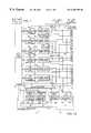
- FIG. 1is a data storage system adapted to operate in a dual-write mode or a non-dual write mode in accordance with the invention
- FIG. 2is a block diagram of an exemplary memory adapted for use in the system of FIG. 1;
- FIG. 3is a block diagram of a rear-end director according to the invention, such director being adapted for use in the system of FIG. 1;
- FIG. 4is a block diagram of a front-end director according to the invention, such director being adapted for use in the system of FIG. 1;
- FIG. 5is a block diagram of a dual-write force HIGH/LOW controller according to the invention and adapted for use in the front-end and rear-end directors of FIGS. 3 and 4;
- FIG. 6is a flow diagram of a program stored in the directors of FIGS. 3 and 4, such program being adapted to place the system of FIG. 1 in a dual-write mode;
- FIG. 7is a flow diagram of a program stored in the directors of FIGS. 3 and 4, such program being adapted to reset the system of FIG. 1 from the dual-write mode to a non-dual write mode;
- FIG. 8is a flow diagram of a program stored in the directors of FIGS. 3 and 4, such program being adapted to place the system of FIG. 1 in a forced HIGH/LOW mode.
- a data storage system 10is shown wherein a host computer 12 is coupled to a bank 14 of disk drives through a system interface 16 .
- the system interface 16includes a system, or cache, memory 18 , having a high address memory sections 18 H and low address memory sections 18 L.
- a plurality of directors 20 0 - 20 15is provided for controlling data transfer between the host computer 12 and the bank 14 of disk drives as such data passes through the system memory 18 .
- the system 10includes a system bus 17 comprising four system busses a top high address memory bus TH, a top low address memory bus TL, a bottom high address memory bus BH, and a bottom low address memory bus BL, described in more detail in co-pending patent application entitled “Data Storage System”, inventors Daniel Castle, et al., filed on the same day as this application, assigned to the same assignee as the present invention, the entire subject mater thereof being incorporated herein by reference. More particularly, high address system busses TH, BH are electrically connected to the high address memory sections 18 H. Low address system busses TL, BL are electrically connected to the low address memory sections 18 L.
- Each one of the directors 20 0 - 20 15is coupled to a pair of the system busses; one bus being a high address bus and the other being a low address bus. Thus, each one of the directors 20 0 - 20 15 is coupled to the pair of the system memory sections 18 H and 18 L.
- each one of the directors 20 0 - 20 15is electrically connected to one of the pair of high address system busses TH, BH and one of the pair of low address system busses TL, BL.
- each one of the directors 20 0 - 20 15is able to address all locations in the entire system memory 18 (i.e., to both the high address memory sections 18 H and the low address memory sections 18 L) and is therefore able to store data in and retrieve data from any storage location in the entire system memory 18 .
- system busses BH, BL, TH, TLprovide data, addresses and memory control (i.e., write enable, read enable) to the memory 18
- system 10also includes a dual-write control signal bus DW which is connected to all the directors, as indicated.
- a rear-end portion of the directorshere directors 20 0 - 20 3 and 20 12 - 20 15 , is electrically connected to the bank 14 of disk drives through I/O adapter cards 22 0 - 22 3 and 22 12 - 22 15 , respectively, and a front-end portion of the directors, here directors 20 4 - 20 11 , is electrically connected to the host computer 12 through I/O adapter cards 22 4 - 22 11 , respectively.
- each end of the busses TH, TL, BH, BLis terminated with a pair of master and slave arbiters, not shown, described in detail in connection with the above-referenced co-pending patent application.
- the system 10is adapted to operate in a number of modes.
- One modeis a non-dual-write mode
- another modeis a dual- write mode
- still another modeis a forced HIGH/LOW mode.
- data to be transferred between the host computer 12 and the bank of disk drives 14is transferred as a series of bursts of such data.
- the directors 20 0 - 20 15store the bursts of the data being transferred between the host computer 12 and the bank of disk drives 14 .
- the stored burst of datais transferred by the director storing such data to one of the two system busses coupled thereto for temporary storage in the system memory 18 .
- the burst of data stored in the directoris transferred sequentially to both of the busses coupled to such director.
- the directorsenable both of the memory sections 18 H and 18 L coupled to both such busses to have written therein, at the same one of the addressable locations, the burst of data transferred sequentially to the bus.
- two copies of the same burst of datais stored in the pair of memory sections 18 H, 18 L for redundancy.
- each one of the directors 20 0 - 20 15is adapted to detect a fault in the transfer of the data between the director and the memory sections 18 H and 18 L. In response to a detected fault between the director and one of the pair of memory sections 18 H, 18 L, each one of the directors is adapted to force subsequent data transfers between the director and the other one of the pair of memory sections.
- director 20 4which is coupled to buses BL and TH, if such director is to transfer a burst of data stored therein to memory section 18 H via system bus TH and a fault in such transferred is detected as with Error Detection and Correction (EDAC) or “time-out” circuitry (not shown) in the memory section 18 H or director 20 4 , such director 20 4 the system 10 is placed by such director 20 4 in the forced HIGH/LOW mode, to be described. More particularly, in this example, the director 20 4 forces all transfers of bursts of the data to the other memory connected thereto, here memory section 18 L via system bus BL until the fault is corrected.
- EDACError Detection and Correction
- the host computer 12issues a write request to one of the front-end directors 20 4 - 20 11 to perform a write command.
- One of the front-end directors 20 4 - 20 11replies to the request and asks the host computer 12 for the data.
- the directordetermines the size of the data and reserves space in the system memory 18 to store the request.
- the front-end directorthen produces control signals to arbitrate for the given bus on either a high address memory system bus (TH or BH) or a low address memory system bus (TL, BL) connected to such front-end director depending on the location in the system memory 18 allocated to store the data and enable the transfer to the system memory 18 .
- the host computer 12then transfers the data, as bursts of data, to the front-end director.
- the front-end directorthen advises the host computer 12 that the transfer is complete.
- the front-end directorlooks up in a Table, not shown, stored in the system memory 18 to determine which one of the rear-end directors 20 0 - 20 3 and 20 12 - 20 15 is to handle this request.
- the Tablemaps the host computer 12 address into an address in the bank 14 of disk drives.
- the front-end directorthen puts a notification in a “mail box” (not shown and stored in the system memory 18 ) for the rear-end director which is to handle the request, the amount of the data and the disk address for the data.
- Other rear-end directorspoll the system memory 18 when they are idle to check their “mail boxes”. If the polled “mail box” indicates a transfer is to be made, the rear-end director processes the request, addresses the disk drive in the bank, reads the data from the system memory 18 and writes it into the addresses of a disk drive in the bank 14 .
- the system 10operates in a reciprocal manner.
- the directors 20 0 - 20 15are configured to place the system 10 in a dual-write mode.
- the directors 20 0 - 20 15store therein bursts of the data to be transferred between the host computer 12 and the bank 14 of disk drives.
- Each burst of data stored in the directoris then transferred to one of the pair of system busses coupled to such director during one memory cycle and, during the next memory cycle, the same burst of data is then transferred again, but this time to the other one of the pair of system busses coupled to such director.
- the same stored burst of datais transferred sequentially to both pairs of system busses coupled to such director.
- the directorsequentially enables both of the memory sections 18 H and 18 L coupled to both such pair of system busses to have written therein, at the same addressable locations, the same data burst which had been sequentiality transferred to each of the pair of system busses coupled to the director. For example, considering director 20 4 , during the dual-write mode, a data burst from the host computer 12 passes to such director 20 4 and becomes stored in such director 20 4 . The stored data burst is then transferred to the system bus BL along with an address into which such data burst is to be written into memory section 18 L, for example, during a system memory cycle. During the next system memory cycle, the same burst of data is transferred to system bus TH with the same addressable location used to for storage in memory sections 18 L.
- the same burst of datais stored in memory section 18 H at the same addressable location as the burst of data was stored in memory section 18 L.
- the burst of data and a copy of such burst of dataare stored in the same addressable location of both memory sections 18 H and 18 L. Consequently, redundant data bursts are stored in the system memory 18 .
- FIG. 2An exemplary one of the memory sections, 18 H, 18 L, here section 18 H, is shown in FIG. 2 to include a plurality of here four DRAM sections coupled to top and bottom busses though bus interfaces and ASIC control logic, as indicated.
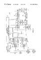
- Each one of the rear-end portion of the directors 20 0 - 20 3 and 20 12 - 20 15is identical in construction, an exemplary one therefor, here rear-end director 200 being shown in FIG. 3 to include a pair of central processing sections, CPU X and CPU Y, a dual port random access memory (RAM) section for storing the bursts of data and which includes a dual port RAM Y coupled to the Y CPU and a dual port RAM X coupled to the X CPU, shared resources (Flash memories, for, among other things, storage of programs the flow diagrams some of which are shown in FIGS.
- RAMrandom access memory
- the X and Y CPU sectionsare coupled to the bank 14 of disk drives (FIG. 1) through I/O adapter card 220 (FIG. 1) via an I/O backplane section interface 28 1 , 28 2 , as indicated.
- the directorhas a primary output port, P, and a secondary output port, S.
- the primary port Pis connected to both I/O backplane interface 28 1 and I/O backplane interface 28 2 .
- the secondary port Sis connected to both I/O backplane interface 28 2 and I/O backplane interface 28 1 .
- the dual port RAM section of director 20 0is coupled to: (1) a high address memory bus, here BH, through data latch 24 H and backplane section interface 22 H; and (2) a low address memory bus, here TL, through data latch 24 L and backplane section interface 22 L, as shown.
- Datai.e., burst of data
- the dual-write force HIGH/LOW control section 30will be described in detail in connection with FIG. 5 .
- section 30is adapted to: (i) provide a global dual-write interrupt (GLB_DW) on the dual-write bus DW in response to a dual-write mode command fed to the system 10 ; (ii) receive a global dual-write interrupt (GLB_DW) produced on the dual-write bus DW by another one of the directors 20 1-20 15 and (iii) in response to the global dual-write interrupt (GLB_DW) received on the dual-write bus DW, (either the GLB_DW it produced or the one produced by any one of the other directors), sequentially place the data burst stored in the dual port RAM on both of the system busses BH, TL connected to such director at the same addressable location.
- GLB_DWglobal dual-write interrupt
- the section 30is configured to that the burst data in the dual port RAM is placed on either one of the two system busses, here either BH or TL, with different addressable locations.
- each one of the directors 20 0 - 20 15is adapted to detect a fault in the transfer of the data between the director and the memory sections 18 H and 18 L. In response to a detected fault between the director and one of the memory sections 18 H, 18 L, each one of the directors is adapted to force subsequent data transfers between the director and the other one of the memories.
- director 20 4which is coupled to buses TL and BH, if such director is to transfer a burst of data stored therein to memory section 18 H via bus BH and a fault in such transferred is detected as with EDAC or “time-out” circuitry, in the memory section 18 H or director 20 4 , the system 10 is placed by such director 20 4 in the force HIGH/LOW mode. More particularly, in this example, the director 20 4 forces all transfers of burst data to the other memory connected thereto, here memory section 18 L via bus TL until the fault is corrected.
- latch enable signalsare produced by the control section 30 sequentially on lines 32 H and 32 L. That is, during one memory cycle, a latch enable signal is produced on, for example, line 32 H and during the next memory cycle a latch enable signal is produced on line 32 L in such example. In response to such latch enable signals, the burst of data in the dual port RAM is stored, in this example, sequentially into data latches 24 H and 24 L, respectively. Further, in the dual-write mode, the latch signals on lines 32 H, 32 L latch a common address on either bus 34 X or bus 34 Y into address latches 26 H or 26 L.
- the address latched into latches 26 H and 26 Lprovide the same address location in the system memory 18 where such data burst is to be stored. It is noted that when the burst of data from the dual port RAM is latched into data latch 24 H and the address for such latched burst of data is latched into address latch 26 H during one memory cycle by the latch enable signal on line 32 H, such latched burst of data along with its address pass though the backplane interface 32 H to the high address memory system bus BH, in this example.
- the same burst of data from the dual port RAMis latched into data latch 24 L and the address for such burst of data is latched into address latch 26 L by the latch enable signal on line 32 L, such latched burst of data along with its address pass though the backplane interface 32 L to the low address memory system bus TL, in this example.
- the burst of data being transferred from the dual port RAM for storage on the system memory 18is here first placed on the bus BH, for example, via data latch 24 H and backplane interface 22 H during one memory cycle and then placed on bus TL via data latch 24 L and backplane interface 22 L during the next memory cycle.
- Each one of the front-end portion of the directors 20 4 - 20 11is identical in construction and is substantially the same as the rear-end directors described above in connection with FIG. 3 .
- an exemplary one thereof, here director 20 4is shown in detail in FIG. 4 with equivalent elements being designated with the same numerical designation as that used in FIG. 3 .
- the exemplary front-end director 20 4is shown to include a pair of central processing sections (i.e., CPU X and CPU Y), a dual port random access memory (RAM) section which includes a dual port RAM Y coupled to the Y CPU and a dual port RAM X coupled to the X CPU, shared resources (Flash memories, etc.), a pair of backplane interfaces 22 H, 22 L, a pair of data latches 24 H, 24 L, a pair of address latches 26 H, 26 L, a pair of I/O backplane interfaces 28 1 , 28 2 , and a dual-write force HIGH/LOW control section 30 (to be described in detail in connection with FIG. 5 ), all arranged as shown.
- the X and Y CPU sectionsare coupled to the host computer 12 (FIG. 1) through I/O adapter card 224 (FIG. 1) via an I/O backplane section interface 28 1 , 28 2 , as indicated.
- the dual port RAM sectionis coupled to: (1) a high address memory bus, here TH, through data latch 24 H and backplane section interface 22 H; and (2) a bottom low address memory bus, here BL, through data latch 24 L and backplane section interface 22 L, as shown.
- Datai.e., burst of data
- THhigh address memory bus
- BLbottom low address memory bus
- section 30is adapted to: (i) provide a global dual-write interrupt (GLB_DW) on the dual-write bus DW in response to a dual-write mode command fed to the system 10 ; (ii) receive a global dual-write interrupt (GLB DW) produced on the dual-write bus DW by another one of the directors 20 1 - 20 15 and (iii) in response to the global dual-write interrupt (GLB_DW) received on the dual-write bus DW (either the GLB_DW it produced or the one produced by any one of the other directors), sequentially place the data burst stored in the dual port RAM on both of the system busses connected to such director at the same addressable location.
- GLB_DWglobal dual-write interrupt
- each one of the directors 20 0 - 20 15is adapted to detect a fault in the transfer of the data between the director and the memory sections 18 H and 18 L. In response to a detected fault between the director and one of the memory sections 18 H, 18 L, each one of the directors is adapted to force subsequent data transfers between the director and the other one of the memory sections.
- the dual-write/Force HIGH/LOW control section 30is shown to include: a pair of dual-write interrupt controllers 40 x , 40 y coupled to the X CPU section and Y CPU section respectively of the director having such control section 30 .
- Each one of the controllers 40 x , 40 yis identical in construction and is configured to: (i) provide a global dual-write interrupt YGLB_DW, XGLB_DW respectively in response to a dual-write mode command fed to the system 10 (FIG. 1) and (ii) receive a dual-write interrupt DW_INT produced on the dual-write bus DW either by the director having the control section 30 or any of the other directors.
- the XGLB_DW and YGLB_DW signalsare fed to an OR gate 42 .
- the output of the OR gate 42is a two bit signal GLB_DW_OUT which is fed to an GTL driver.
- the output of the GTL driveris the global dual-write signal GLB_DW and is fed to the other directors, via the dual write bus DW, and the director producing the GLB_DW signal via GTL receiver which produces the signal DW_INT for the pair of dual-write interrupt controllers 40 x , 40 y .
- the dual-write/Force HIGH/LOW control section 30also includes a pair of address gate arrays 46 x and 46 y coupled to the X and Y interrupt controllers 40 x , 40 y , respectively, as shown.
- the pair of address gate arrays 46 x and 46 yprovide the system memory 18 addresses for the bursts of data stored in the dual port RAM/ During the dual-write mode, a common address for each burst of data, as discussed above.
- the outputs of the address gate arrays 56 x and 64 yare fed to a logic section 50 .
- the logic section 50produces the latch signals on lines 32 H, 32 L and the X and Y DRAM control signals (e.g. read/write/address) for the DRAM section.
- the controllers 40 x , 40 yprovide addresses for the burst of data being coupled from the dual port DRAM section (FIGS. 3 and 4) to the data latches 24 H, 24 L on busses 34 x and 34 y , respectively.
- the addresses provided by the pair of address gate arrays 46 x and 46 y on busses 34 x and 34 yare fed to the address latches 26 H, 26 L as shown in FIGS. 3 and 4, as discussed above. It is noted that the addresses on busses 34 x , 34 y is latched into the address latches 26 H and 26 L selectively in accordance with the latch signals on lines 32 H and 32 L.
- the burst of data in the dual port RAM sectionis placed sequentially into data latches 24 H and 24 L.
- data latch 24 Hfor example, an address for such data is latched into address latch 26 H.
- address latch 26 Lthe same address which had in the previous memory cycle had been latched into address latch 26 H is latched into address latch 26 L.
- the address latched into the address latches 26 H and 26 Lare independent from each other during successive memory cycles.
- FIG. 6a flow diagram of a program stored in the directors 20 0 - 20 15 is shown, such program being adapted to place the system 10 (FIG. 1) in the dual-write mode.
- the system 10is checked to determine whether there is a balance in system memory 18 capacity between the high address memory section 18 H and the low address memory section 18 L (i.e, the sections have a memory capacity balance). If there is an imbalance detected, (Step 602 ) the system 10 is powered-down by the user (Step 604 ) and additional memory capacity is added to a memory capacity deficient one of the sections 18 L or 18 H.
- a dual-write mode of operationis selected when the user wishes have redundant data in the system memory 18 , i.e., the same burst of data in each of the memory sections 18 L and 18 H.
- the same burst of transferred datais available in the other one of the memory sections 18 H, 18 L.
- each of the directors 20 0 - 20 15must know that the system 10 is being placed in the dual-write mode.
- a signalis sent to both X and Y CPUs in such director (Step 606 ).
- the X and Y interrupt control sections 40 x and 40 Yhave a state machine register (not shown) change from an initial, reset, logic 0 state to a logic 1 on one of the two bits thereof. If such interrupt exists at the next system clock pulse, the state machine registers of both the X and Y interrupt control sections 40 x and 40 y have the second bit change from an initial logic 0 state to a logic 1 state.
- the logic 00 state on bus GLB_DW*is fed, via a GTL driver, to: the dual-write bus DW (FIG. 5) as a global dual-write signal, GLB_DW*; and back to the X and Y interrupt control sections 40 x and 40 y via a GTL receiver, as indicated in FIG. 5 .
- the GLB_DW* signalindicates to this director, and all other directors, that a dual-write mode has been requested, i.e., a GLB_DW* signal has been asserted on the dual-write bus DW (Step 614 , FIG. 6 ).
- the GLB_DW*, 11 logic signal, on the dual-writeis fed to the interrupt issuing one of the directors 20 0 - 20 15 and all other directors 20 0 - 20 15 .
- Each one of the directors 20 0 - 20 15determines whether the state machine registers in the X and Y interrupt control sections 40 x and 40 y thereof is in the logic 00 condition. While the interrupt issuing one of the directors 20 0 - 20 15 has the state machine registers thereof in the 00 logic condition, the other one of the issuing one of the directors 20 0 - 20 15 must wait two system clock pulses before the state machines thereof are placed in the logic 00 condition (Step 613 ).
- Step 615the interrupt control sections 40 x and 40 y send the global dual-write mode signal indication to the address gate array controllers 46 x , 46 y (FIG. 5) (Step 616 ).
- Step 700a flow diagram of a program stored in the directors 20 0 - 20 15 is shown, such program being adapted to reset the system 10 (FIG. 1) from the dual-write mode to a non-dual-write mode.
- the softwareenters the “turn off” global dual-write routine (Step 700 ). Interrupts are fed to the pair of Y and X interrupt controllers 40 x , 40 y (FIG. 5, Step 702 ), and if after two system clock pulses the interrupt is proper (Step 704 ), the GLB_DW* signal on the dual-write bus DW is de-asserted (Step 706 ).
- the dual-write control sections 30are wire-ORd on the dual-write bus DW, it is necessary for all controllers 20 0 - 20 15 to have the GLB_DW* signal fed to the dual-write bus DW in a low, i.e., de-asserted logic state before all directors 20 0 - 20 15 are placed in the reset). That is, the dual-write mode is disabled and the system 10 is placed in the non-dual-write mode, Step 708 .
- the X. and Y interrupt controllers 40 x , 40 yindicate to the address gate array controllers 46 x , 46 y that the system 10 is now in the non-dual-write mode (Step 710 ).
- FIG. 8a flow diagram is shown of a program stored in the directors 20 0 - 20 15 , such program being adapted to place the system 10 (FIG. 1) in a forced HIGH/LOW mode.
- the system 10is operating normally in the dual-write mode (Step 800 ).
- the controllermeasure the number of faults, or “time-out” errors reported to them (Step 802 ). If none of the directors 20 0 - 20 15 is having reported to it errors or “time-outs” in less than a predetermined number, the system continues in the dual-write mode (Step 804 , 806 ).
- Step 806that director initiates the forced HIGH/LOW mode of operation for the system 10 .
- Step 608the state machine registers of both the X and Y interrupt control sections 40 x and 40 y produce a binary 11 logic condition on busses either: (a) either busses XGLB_FOR_HI* and YGLB_FOR_HI*; or (b) either busses XGLB_FOR_LO and YGLB_FOR_LO*, respectively (Step 810 ), depending on whether the faults are with transfers to the high address memory bus or the low address memory bus (Step 810 ). (It is noted the logic is here “active” low logic indicated in FIG.
- NAND gates 60 HI and 60 LOcan have their outputs disabled via a user activated signal, DIS_IF*, which is fed to open collector drivers 61 HI and 61 LO, as indicated.
- DIS_IF*user activated signal
- an interruptis generated when any one of the directors 20 0 - 20 15 asserts a force high/low interrupt (i.e., either a GLB_FOR_LO* or GLB_FOR_HI* signal, FIG. 5 (Step 814 ).
- the directors 20 0 - 20 15are now in the force HIGH/LOW mode (i.e., dual-write mode is disabled) and the X and Y interrupt controllers 40 x and 40 y indicate to the address gate array controllers 46 x and 46 y where the force HIGH and ⁇ or FORCE LOW condition is selected.
- the address gate array controllers 46 x and 46 ythen provide signals on the Y_TB_MEM* and X_TB_MEM* busses, respectively, to thereby enable the logic 50 to produce latch signals on lines 32 H or 32 L; the former being produced when in the force HIGH condition (i.e., excessive errors or time-outs to the low address memory section 18 L) and the latter being produced when in the force LOW condition (i.e., excessive errors or time-outs to the high address memory section 18 H), Step 816 .
Landscapes
- Engineering & Computer Science (AREA)
- Theoretical Computer Science (AREA)
- Physics & Mathematics (AREA)
- General Engineering & Computer Science (AREA)
- General Physics & Mathematics (AREA)
- Quality & Reliability (AREA)
- Techniques For Improving Reliability Of Storages (AREA)
- Bus Control (AREA)
Abstract
Description
Claims (9)
Priority Applications (7)
| Application Number | Priority Date | Filing Date | Title |
|---|---|---|---|
| US09/223,417US6493795B1 (en) | 1998-12-30 | 1998-12-30 | Data storage system |
| EP99966711AEP1058888B1 (en) | 1998-12-30 | 1999-12-29 | Data storage system |
| PCT/US1999/031178WO2000039690A1 (en) | 1998-12-30 | 1999-12-29 | Data storage system |
| DE69930307TDE69930307T2 (en) | 1998-12-30 | 1999-12-29 | DATA STORAGE SYSTEM |
| KR1020007009616AKR100560552B1 (en) | 1998-12-30 | 1999-12-29 | Data storage system |
| JP2000591518AJP3742753B2 (en) | 1998-12-30 | 1999-12-29 | Data storage system |
| JP2005235337AJP2006024230A (en) | 1998-12-30 | 2005-08-15 | Data storage system |
Applications Claiming Priority (1)
| Application Number | Priority Date | Filing Date | Title |
|---|---|---|---|
| US09/223,417US6493795B1 (en) | 1998-12-30 | 1998-12-30 | Data storage system |
Publications (1)
| Publication Number | Publication Date |
|---|---|
| US6493795B1true US6493795B1 (en) | 2002-12-10 |
Family
ID=22836406
Family Applications (1)
| Application Number | Title | Priority Date | Filing Date |
|---|---|---|---|
| US09/223,417Expired - LifetimeUS6493795B1 (en) | 1998-12-30 | 1998-12-30 | Data storage system |
Country Status (6)
| Country | Link |
|---|---|
| US (1) | US6493795B1 (en) |
| EP (1) | EP1058888B1 (en) |
| JP (2) | JP3742753B2 (en) |
| KR (1) | KR100560552B1 (en) |
| DE (1) | DE69930307T2 (en) |
| WO (1) | WO2000039690A1 (en) |
Cited By (14)
| Publication number | Priority date | Publication date | Assignee | Title |
|---|---|---|---|---|
| US20030065733A1 (en)* | 2001-09-28 | 2003-04-03 | Pecone Victor Key | Modular architecture for a network storage controller |
| US20030065836A1 (en)* | 2001-09-28 | 2003-04-03 | Pecone Victor Key | Controller data sharing using a modular DMA architecture |
| US20040114690A1 (en)* | 2002-12-06 | 2004-06-17 | Stephen Gordon | Managing bursts of data |
| US20040177126A1 (en)* | 2003-02-18 | 2004-09-09 | Chaparral Network Storage, Inc. | Broadcast bridge apparatus for transferring data to redundant memory subsystems in a storage controller |
| US20040186931A1 (en)* | 2001-11-09 | 2004-09-23 | Gene Maine | Transferring data using direct memory access |
| US20050097392A1 (en)* | 1999-09-29 | 2005-05-05 | Miklos Sandorfi | Central processing unit |
| US20050102557A1 (en)* | 2001-09-28 | 2005-05-12 | Dot Hill Systems Corporation | Apparatus and method for adopting an orphan I/O port in a redundant storage controller |
| US20060106982A1 (en)* | 2001-09-28 | 2006-05-18 | Dot Hill Systems Corporation | Certified memory-to-memory data transfer between active-active raid controllers |
| US20060161709A1 (en)* | 2005-01-20 | 2006-07-20 | Dot Hill Systems Corporation | Safe message transfers on PCI-Express link from RAID controller to receiver-programmable window of partner RAID controller CPU memory |
| US20060161707A1 (en)* | 2005-01-20 | 2006-07-20 | Dot Hill Systems Corporation | Method for efficient inter-processor communication in an active-active RAID system using PCI-express links |
| US20060277347A1 (en)* | 2001-09-28 | 2006-12-07 | Dot Hill Systems Corporation | RAID system for performing efficient mirrored posted-write operations |
| US20080005470A1 (en)* | 2006-06-30 | 2008-01-03 | Dot Hill Systems Corporation | System and method for sharing sata drives in active-active raid controller system |
| US20080201616A1 (en)* | 2007-02-20 | 2008-08-21 | Dot Hill Systems Corporation | Redundant storage controller system with enhanced failure analysis capability |
| US8365023B2 (en) | 2011-04-29 | 2013-01-29 | International Business Machines Corporation | Runtime dynamic performance skew elimination |
Families Citing this family (8)
| Publication number | Priority date | Publication date | Assignee | Title |
|---|---|---|---|---|
| US6519739B1 (en) | 1999-09-29 | 2003-02-11 | Emc Corporation | Fault detector |
| US6543029B1 (en) | 1999-09-29 | 2003-04-01 | Emc Corporation | Error corrector |
| US6915394B1 (en) | 1999-09-29 | 2005-07-05 | Emc Corporation | Microprocessor interface |
| US6581137B1 (en) | 1999-09-29 | 2003-06-17 | Emc Corporation | Data storage system |
| US6735655B1 (en) | 1999-09-29 | 2004-05-11 | Emc Corporation | Interrupt request controller |
| US6779130B2 (en) | 2001-09-13 | 2004-08-17 | International Business Machines Corporation | Method and system for root filesystem replication |
| US20030217211A1 (en)* | 2002-05-14 | 2003-11-20 | Rust Robert A. | Controller communications over an always-on controller interconnect |
| US20060002482A1 (en)* | 2004-06-30 | 2006-01-05 | Clinton Walker | Signal drive de-emphasis for memory bus |
Citations (15)
| Publication number | Priority date | Publication date | Assignee | Title |
|---|---|---|---|---|
| US4654819A (en)* | 1982-12-09 | 1987-03-31 | Sequoia Systems, Inc. | Memory back-up system |
| US4819154A (en)* | 1982-12-09 | 1989-04-04 | Sequoia Systems, Inc. | Memory back up system with one cache memory and two physically separated main memories |
| US5206939A (en)* | 1990-09-24 | 1993-04-27 | Emc Corporation | System and method for disk mapping and data retrieval |
| US5457786A (en)* | 1990-07-03 | 1995-10-10 | Texas Instruments Incorporated | Serial data interface with circular buffer |
| US5682509A (en)* | 1995-12-13 | 1997-10-28 | Ast Research, Inc. | Bus interface to a RAID architecture |
| US5787243A (en)* | 1994-06-10 | 1998-07-28 | Texas Micro, Inc. | Main memory system and checkpointing protocol for fault-tolerant computer system |
| US5787265A (en) | 1995-09-28 | 1998-07-28 | Emc Corporation | Bus arbitration system having a pair of logic networks to control data transfer between a memory and a pair of buses |
| US5819054A (en) | 1993-06-30 | 1998-10-06 | Hitachi, Ltd. | Storage system realizing scalability and fault tolerance |
| US5838891A (en)* | 1995-03-22 | 1998-11-17 | Mitsubishi Denki Kabushiki Kaisha | Data storage system and storage managing method |
| US5864657A (en)* | 1995-11-29 | 1999-01-26 | Texas Micro, Inc. | Main memory system and checkpointing protocol for fault-tolerant computer system |
| US5887270A (en)* | 1995-11-21 | 1999-03-23 | Emc Corporation | Fault tolerant controller system and method |
| US5895485A (en)* | 1997-02-24 | 1999-04-20 | Eccs, Inc. | Method and device using a redundant cache for preventing the loss of dirty data |
| US5935258A (en)* | 1997-03-04 | 1999-08-10 | Micron Electronics, Inc. | Apparatus for allowing data transfers with a memory having defective storage locations |
| US5953745A (en)* | 1996-11-27 | 1999-09-14 | International Business Machines Corporation | Redundant memory array |
| US5991852A (en)* | 1996-10-28 | 1999-11-23 | Mti Technology Corporation | Cache ram using a secondary controller and switching circuit and improved chassis arrangement |
- 1998
- 1998-12-30USUS09/223,417patent/US6493795B1/ennot_activeExpired - Lifetime
- 1999
- 1999-12-29JPJP2000591518Apatent/JP3742753B2/ennot_activeExpired - Fee Related
- 1999-12-29WOPCT/US1999/031178patent/WO2000039690A1/enactiveIP Right Grant
- 1999-12-29KRKR1020007009616Apatent/KR100560552B1/ennot_activeExpired - Lifetime
- 1999-12-29EPEP99966711Apatent/EP1058888B1/ennot_activeExpired - Lifetime
- 1999-12-29DEDE69930307Tpatent/DE69930307T2/ennot_activeExpired - Lifetime
- 2005
- 2005-08-15JPJP2005235337Apatent/JP2006024230A/enactivePending
Patent Citations (15)
| Publication number | Priority date | Publication date | Assignee | Title |
|---|---|---|---|---|
| US4819154A (en)* | 1982-12-09 | 1989-04-04 | Sequoia Systems, Inc. | Memory back up system with one cache memory and two physically separated main memories |
| US4654819A (en)* | 1982-12-09 | 1987-03-31 | Sequoia Systems, Inc. | Memory back-up system |
| US5457786A (en)* | 1990-07-03 | 1995-10-10 | Texas Instruments Incorporated | Serial data interface with circular buffer |
| US5206939A (en)* | 1990-09-24 | 1993-04-27 | Emc Corporation | System and method for disk mapping and data retrieval |
| US5819054A (en) | 1993-06-30 | 1998-10-06 | Hitachi, Ltd. | Storage system realizing scalability and fault tolerance |
| US5787243A (en)* | 1994-06-10 | 1998-07-28 | Texas Micro, Inc. | Main memory system and checkpointing protocol for fault-tolerant computer system |
| US5838891A (en)* | 1995-03-22 | 1998-11-17 | Mitsubishi Denki Kabushiki Kaisha | Data storage system and storage managing method |
| US5787265A (en) | 1995-09-28 | 1998-07-28 | Emc Corporation | Bus arbitration system having a pair of logic networks to control data transfer between a memory and a pair of buses |
| US5887270A (en)* | 1995-11-21 | 1999-03-23 | Emc Corporation | Fault tolerant controller system and method |
| US5864657A (en)* | 1995-11-29 | 1999-01-26 | Texas Micro, Inc. | Main memory system and checkpointing protocol for fault-tolerant computer system |
| US5682509A (en)* | 1995-12-13 | 1997-10-28 | Ast Research, Inc. | Bus interface to a RAID architecture |
| US5991852A (en)* | 1996-10-28 | 1999-11-23 | Mti Technology Corporation | Cache ram using a secondary controller and switching circuit and improved chassis arrangement |
| US5953745A (en)* | 1996-11-27 | 1999-09-14 | International Business Machines Corporation | Redundant memory array |
| US5895485A (en)* | 1997-02-24 | 1999-04-20 | Eccs, Inc. | Method and device using a redundant cache for preventing the loss of dirty data |
| US5935258A (en)* | 1997-03-04 | 1999-08-10 | Micron Electronics, Inc. | Apparatus for allowing data transfers with a memory having defective storage locations |
Cited By (34)
| Publication number | Priority date | Publication date | Assignee | Title |
|---|---|---|---|---|
| US20050097392A1 (en)* | 1999-09-29 | 2005-05-05 | Miklos Sandorfi | Central processing unit |
| US7302532B2 (en) | 1999-09-29 | 2007-11-27 | Emc Corporation | Central processing unit |
| US20060106982A1 (en)* | 2001-09-28 | 2006-05-18 | Dot Hill Systems Corporation | Certified memory-to-memory data transfer between active-active raid controllers |
| US7146448B2 (en) | 2001-09-28 | 2006-12-05 | Dot Hill Systems Corporation | Apparatus and method for adopting an orphan I/O port in a redundant storage controller |
| US7558897B2 (en) | 2001-09-28 | 2009-07-07 | Dot Hill Systems Corporation | Method for adopting an orphan I/O port in a redundant storage controller |
| US7536495B2 (en) | 2001-09-28 | 2009-05-19 | Dot Hill Systems Corporation | Certified memory-to-memory data transfer between active-active raid controllers |
| US7437493B2 (en) | 2001-09-28 | 2008-10-14 | Dot Hill Systems Corp. | Modular architecture for a network storage controller |
| US20050102557A1 (en)* | 2001-09-28 | 2005-05-12 | Dot Hill Systems Corporation | Apparatus and method for adopting an orphan I/O port in a redundant storage controller |
| US20030065733A1 (en)* | 2001-09-28 | 2003-04-03 | Pecone Victor Key | Modular architecture for a network storage controller |
| US7062591B2 (en) | 2001-09-28 | 2006-06-13 | Dot Hill Systems Corp. | Controller data sharing using a modular DMA architecture |
| US20030065836A1 (en)* | 2001-09-28 | 2003-04-03 | Pecone Victor Key | Controller data sharing using a modular DMA architecture |
| US7340555B2 (en) | 2001-09-28 | 2008-03-04 | Dot Hill Systems Corporation | RAID system for performing efficient mirrored posted-write operations |
| US20060282701A1 (en)* | 2001-09-28 | 2006-12-14 | Dot Hill Systems Corporation | Method for adopting an orphan i/o port in a redundant storage controller |
| US20060277347A1 (en)* | 2001-09-28 | 2006-12-07 | Dot Hill Systems Corporation | RAID system for performing efficient mirrored posted-write operations |
| US7380115B2 (en) | 2001-11-09 | 2008-05-27 | Dot Hill Systems Corp. | Transferring data using direct memory access |
| US20040186931A1 (en)* | 2001-11-09 | 2004-09-23 | Gene Maine | Transferring data using direct memory access |
| US7583732B2 (en)* | 2002-12-06 | 2009-09-01 | Broadcom Corporation | Managing bursts of data |
| US20040114690A1 (en)* | 2002-12-06 | 2004-06-17 | Stephen Gordon | Managing bursts of data |
| US7143227B2 (en) | 2003-02-18 | 2006-11-28 | Dot Hill Systems Corporation | Broadcast bridge apparatus for transferring data to redundant memory subsystems in a storage controller |
| US20040177126A1 (en)* | 2003-02-18 | 2004-09-09 | Chaparral Network Storage, Inc. | Broadcast bridge apparatus for transferring data to redundant memory subsystems in a storage controller |
| WO2004074996A3 (en)* | 2003-02-18 | 2004-12-29 | Chapparal Network Storage Inc | Broadcast bridge apparatus for transferring data to subsystems in a storage controller |
| US7543096B2 (en) | 2005-01-20 | 2009-06-02 | Dot Hill Systems Corporation | Safe message transfers on PCI-Express link from RAID controller to receiver-programmable window of partner RAID controller CPU memory |
| US20060161707A1 (en)* | 2005-01-20 | 2006-07-20 | Dot Hill Systems Corporation | Method for efficient inter-processor communication in an active-active RAID system using PCI-express links |
| US20060161709A1 (en)* | 2005-01-20 | 2006-07-20 | Dot Hill Systems Corporation | Safe message transfers on PCI-Express link from RAID controller to receiver-programmable window of partner RAID controller CPU memory |
| US7315911B2 (en) | 2005-01-20 | 2008-01-01 | Dot Hill Systems Corporation | Method for efficient inter-processor communication in an active-active RAID system using PCI-express links |
| US20080005470A1 (en)* | 2006-06-30 | 2008-01-03 | Dot Hill Systems Corporation | System and method for sharing sata drives in active-active raid controller system |
| US7536508B2 (en) | 2006-06-30 | 2009-05-19 | Dot Hill Systems Corporation | System and method for sharing SATA drives in active-active RAID controller system |
| US20080201616A1 (en)* | 2007-02-20 | 2008-08-21 | Dot Hill Systems Corporation | Redundant storage controller system with enhanced failure analysis capability |
| US7681089B2 (en) | 2007-02-20 | 2010-03-16 | Dot Hill Systems Corporation | Redundant storage controller system with enhanced failure analysis capability |
| US8365023B2 (en) | 2011-04-29 | 2013-01-29 | International Business Machines Corporation | Runtime dynamic performance skew elimination |
| US8443241B2 (en) | 2011-04-29 | 2013-05-14 | International Business Machines Corporation | Runtime dynamic performance skew elimination |
| US8719645B2 (en) | 2011-04-29 | 2014-05-06 | International Business Machines Corporation | Runtime dynamic performance skew elimination |
| US8738975B2 (en) | 2011-04-29 | 2014-05-27 | International Business Machines Corporation | Runtime dynamic performance skew elimination |
| US9104316B2 (en) | 2011-04-29 | 2015-08-11 | International Business Machines Corporation | Runtime dynamic performance skew elimination |
Also Published As
| Publication number | Publication date |
|---|---|
| DE69930307D1 (en) | 2006-05-04 |
| WO2000039690A9 (en) | 2001-09-07 |
| KR20010041461A (en) | 2001-05-25 |
| JP3742753B2 (en) | 2006-02-08 |
| WO2000039690A1 (en) | 2000-07-06 |
| JP2002533834A (en) | 2002-10-08 |
| KR100560552B1 (en) | 2006-03-15 |
| JP2006024230A (en) | 2006-01-26 |
| EP1058888A1 (en) | 2000-12-13 |
| DE69930307T2 (en) | 2006-11-30 |
| EP1058888B1 (en) | 2006-03-08 |
Similar Documents
| Publication | Publication Date | Title |
|---|---|---|
| US6493795B1 (en) | Data storage system | |
| US7055054B2 (en) | Fail-over of multiple memory blocks in multiple memory modules in computer system | |
| US6543029B1 (en) | Error corrector | |
| US6957285B2 (en) | Data storage system | |
| US5961660A (en) | Method and apparatus for optimizing ECC memory performance | |
| US6961818B1 (en) | Method, system and computer program product for managing data in a mirrored cache using an access balancing technique | |
| US6604171B1 (en) | Managing a cache memory | |
| US5606662A (en) | Auto DRAM parity enable/disable mechanism | |
| US6578128B1 (en) | Address management for a shared memory region on a multi-processor controller board | |
| US6581137B1 (en) | Data storage system | |
| US5822777A (en) | Dual bus data storage system having an addressable memory with timer controller fault detection of data transfer between the memory and the buses | |
| US6347365B1 (en) | Data storage system having a[n] memory responsive to clock pulses produced on a bus and clock pulses produced by an internal clock | |
| US6397281B1 (en) | Bus arbitration system | |
| US6459292B1 (en) | Testing system for semiconductor device | |
| US6519739B1 (en) | Fault detector | |
| US4041460A (en) | Multi-processor data processing system peripheral equipment access units | |
| US6735655B1 (en) | Interrupt request controller | |
| US7302532B2 (en) | Central processing unit | |
| US6249878B1 (en) | Data storage system | |
| US6502149B2 (en) | Plural bus data storage system | |
| US6516370B1 (en) | Data storage system | |
| US5850528A (en) | Bus timing protocol for a data storage system | |
| US6418511B1 (en) | Large capacity data storage systems using redundant buses | |
| US6738842B1 (en) | System having plural processors and a uni-cast/broadcast communication arrangement | |
| US6643722B1 (en) | Data storage system having director boards with plural processors |
Legal Events
| Date | Code | Title | Description |
|---|---|---|---|
| AS | Assignment | Owner name:EMC CORPORATION, MASSACHUSETTS Free format text:ASSIGNMENT OF ASSIGNORS INTEREST;ASSIGNORS:ARSENAULT, BRIAN;TUNG, VICTOR W.;KINNE, JEFFREY STODDARD;REEL/FRAME:009687/0282 Effective date:19981229 | |
| STCF | Information on status: patent grant | Free format text:PATENTED CASE | |
| FPAY | Fee payment | Year of fee payment:4 | |
| FPAY | Fee payment | Year of fee payment:8 | |
| FPAY | Fee payment | Year of fee payment:12 | |
| AS | Assignment | Owner name:THE BANK OF NEW YORK MELLON TRUST COMPANY, N.A., AS NOTES COLLATERAL AGENT, TEXAS Free format text:SECURITY AGREEMENT;ASSIGNORS:ASAP SOFTWARE EXPRESS, INC.;AVENTAIL LLC;CREDANT TECHNOLOGIES, INC.;AND OTHERS;REEL/FRAME:040136/0001 Effective date:20160907 Owner name:CREDIT SUISSE AG, CAYMAN ISLANDS BRANCH, AS COLLATERAL AGENT, NORTH CAROLINA Free format text:SECURITY AGREEMENT;ASSIGNORS:ASAP SOFTWARE EXPRESS, INC.;AVENTAIL LLC;CREDANT TECHNOLOGIES, INC.;AND OTHERS;REEL/FRAME:040134/0001 Effective date:20160907 Owner name:CREDIT SUISSE AG, CAYMAN ISLANDS BRANCH, AS COLLAT Free format text:SECURITY AGREEMENT;ASSIGNORS:ASAP SOFTWARE EXPRESS, INC.;AVENTAIL LLC;CREDANT TECHNOLOGIES, INC.;AND OTHERS;REEL/FRAME:040134/0001 Effective date:20160907 Owner name:THE BANK OF NEW YORK MELLON TRUST COMPANY, N.A., A Free format text:SECURITY AGREEMENT;ASSIGNORS:ASAP SOFTWARE EXPRESS, INC.;AVENTAIL LLC;CREDANT TECHNOLOGIES, INC.;AND OTHERS;REEL/FRAME:040136/0001 Effective date:20160907 | |
| AS | Assignment | Owner name:EMC IP HOLDING COMPANY LLC, MASSACHUSETTS Free format text:ASSIGNMENT OF ASSIGNORS INTEREST;ASSIGNOR:EMC CORPORATION;REEL/FRAME:040203/0001 Effective date:20160906 | |
| AS | Assignment | Owner name:WYSE TECHNOLOGY L.L.C., CALIFORNIA Free format text:RELEASE BY SECURED PARTY;ASSIGNOR:CREDIT SUISSE AG, CAYMAN ISLANDS BRANCH;REEL/FRAME:058216/0001 Effective date:20211101 Owner name:SCALEIO LLC, MASSACHUSETTS Free format text:RELEASE BY SECURED PARTY;ASSIGNOR:CREDIT SUISSE AG, CAYMAN ISLANDS BRANCH;REEL/FRAME:058216/0001 Effective date:20211101 Owner name:MOZY, INC., WASHINGTON Free format text:RELEASE BY SECURED PARTY;ASSIGNOR:CREDIT SUISSE AG, CAYMAN ISLANDS BRANCH;REEL/FRAME:058216/0001 Effective date:20211101 Owner name:MAGINATICS LLC, CALIFORNIA Free format text:RELEASE BY SECURED PARTY;ASSIGNOR:CREDIT SUISSE AG, CAYMAN ISLANDS BRANCH;REEL/FRAME:058216/0001 Effective date:20211101 Owner name:FORCE10 NETWORKS, INC., CALIFORNIA Free format text:RELEASE BY SECURED PARTY;ASSIGNOR:CREDIT SUISSE AG, CAYMAN ISLANDS BRANCH;REEL/FRAME:058216/0001 Effective date:20211101 Owner name:EMC IP HOLDING COMPANY LLC, TEXAS Free format text:RELEASE BY SECURED PARTY;ASSIGNOR:CREDIT SUISSE AG, CAYMAN ISLANDS BRANCH;REEL/FRAME:058216/0001 Effective date:20211101 Owner name:EMC CORPORATION, MASSACHUSETTS Free format text:RELEASE BY SECURED PARTY;ASSIGNOR:CREDIT SUISSE AG, CAYMAN ISLANDS BRANCH;REEL/FRAME:058216/0001 Effective date:20211101 Owner name:DELL SYSTEMS CORPORATION, TEXAS Free format text:RELEASE BY SECURED PARTY;ASSIGNOR:CREDIT SUISSE AG, CAYMAN ISLANDS BRANCH;REEL/FRAME:058216/0001 Effective date:20211101 Owner name:DELL SOFTWARE INC., CALIFORNIA Free format text:RELEASE BY SECURED PARTY;ASSIGNOR:CREDIT SUISSE AG, CAYMAN ISLANDS BRANCH;REEL/FRAME:058216/0001 Effective date:20211101 Owner name:DELL PRODUCTS L.P., TEXAS Free format text:RELEASE BY SECURED PARTY;ASSIGNOR:CREDIT SUISSE AG, CAYMAN ISLANDS BRANCH;REEL/FRAME:058216/0001 Effective date:20211101 Owner name:DELL MARKETING L.P., TEXAS Free format text:RELEASE BY SECURED PARTY;ASSIGNOR:CREDIT SUISSE AG, CAYMAN ISLANDS BRANCH;REEL/FRAME:058216/0001 Effective date:20211101 Owner name:DELL INTERNATIONAL, L.L.C., TEXAS Free format text:RELEASE BY SECURED PARTY;ASSIGNOR:CREDIT SUISSE AG, CAYMAN ISLANDS BRANCH;REEL/FRAME:058216/0001 Effective date:20211101 Owner name:DELL USA L.P., TEXAS Free format text:RELEASE BY SECURED PARTY;ASSIGNOR:CREDIT SUISSE AG, CAYMAN ISLANDS BRANCH;REEL/FRAME:058216/0001 Effective date:20211101 Owner name:CREDANT TECHNOLOGIES, INC., TEXAS Free format text:RELEASE BY SECURED PARTY;ASSIGNOR:CREDIT SUISSE AG, CAYMAN ISLANDS BRANCH;REEL/FRAME:058216/0001 Effective date:20211101 Owner name:AVENTAIL LLC, CALIFORNIA Free format text:RELEASE BY SECURED PARTY;ASSIGNOR:CREDIT SUISSE AG, CAYMAN ISLANDS BRANCH;REEL/FRAME:058216/0001 Effective date:20211101 Owner name:ASAP SOFTWARE EXPRESS, INC., ILLINOIS Free format text:RELEASE BY SECURED PARTY;ASSIGNOR:CREDIT SUISSE AG, CAYMAN ISLANDS BRANCH;REEL/FRAME:058216/0001 Effective date:20211101 | |
| AS | Assignment | Owner name:SCALEIO LLC, MASSACHUSETTS Free format text:RELEASE OF SECURITY INTEREST IN PATENTS PREVIOUSLY RECORDED AT REEL/FRAME (040136/0001);ASSIGNOR:THE BANK OF NEW YORK MELLON TRUST COMPANY, N.A., AS NOTES COLLATERAL AGENT;REEL/FRAME:061324/0001 Effective date:20220329 Owner name:EMC IP HOLDING COMPANY LLC (ON BEHALF OF ITSELF AND AS SUCCESSOR-IN-INTEREST TO MOZY, INC.), TEXAS Free format text:RELEASE OF SECURITY INTEREST IN PATENTS PREVIOUSLY RECORDED AT REEL/FRAME (040136/0001);ASSIGNOR:THE BANK OF NEW YORK MELLON TRUST COMPANY, N.A., AS NOTES COLLATERAL AGENT;REEL/FRAME:061324/0001 Effective date:20220329 Owner name:EMC CORPORATION (ON BEHALF OF ITSELF AND AS SUCCESSOR-IN-INTEREST TO MAGINATICS LLC), MASSACHUSETTS Free format text:RELEASE OF SECURITY INTEREST IN PATENTS PREVIOUSLY RECORDED AT REEL/FRAME (040136/0001);ASSIGNOR:THE BANK OF NEW YORK MELLON TRUST COMPANY, N.A., AS NOTES COLLATERAL AGENT;REEL/FRAME:061324/0001 Effective date:20220329 Owner name:DELL MARKETING CORPORATION (SUCCESSOR-IN-INTEREST TO FORCE10 NETWORKS, INC. AND WYSE TECHNOLOGY L.L.C.), TEXAS Free format text:RELEASE OF SECURITY INTEREST IN PATENTS PREVIOUSLY RECORDED AT REEL/FRAME (040136/0001);ASSIGNOR:THE BANK OF NEW YORK MELLON TRUST COMPANY, N.A., AS NOTES COLLATERAL AGENT;REEL/FRAME:061324/0001 Effective date:20220329 Owner name:DELL PRODUCTS L.P., TEXAS Free format text:RELEASE OF SECURITY INTEREST IN PATENTS PREVIOUSLY RECORDED AT REEL/FRAME (040136/0001);ASSIGNOR:THE BANK OF NEW YORK MELLON TRUST COMPANY, N.A., AS NOTES COLLATERAL AGENT;REEL/FRAME:061324/0001 Effective date:20220329 Owner name:DELL INTERNATIONAL L.L.C., TEXAS Free format text:RELEASE OF SECURITY INTEREST IN PATENTS PREVIOUSLY RECORDED AT REEL/FRAME (040136/0001);ASSIGNOR:THE BANK OF NEW YORK MELLON TRUST COMPANY, N.A., AS NOTES COLLATERAL AGENT;REEL/FRAME:061324/0001 Effective date:20220329 Owner name:DELL USA L.P., TEXAS Free format text:RELEASE OF SECURITY INTEREST IN PATENTS PREVIOUSLY RECORDED AT REEL/FRAME (040136/0001);ASSIGNOR:THE BANK OF NEW YORK MELLON TRUST COMPANY, N.A., AS NOTES COLLATERAL AGENT;REEL/FRAME:061324/0001 Effective date:20220329 Owner name:DELL MARKETING L.P. (ON BEHALF OF ITSELF AND AS SUCCESSOR-IN-INTEREST TO CREDANT TECHNOLOGIES, INC.), TEXAS Free format text:RELEASE OF SECURITY INTEREST IN PATENTS PREVIOUSLY RECORDED AT REEL/FRAME (040136/0001);ASSIGNOR:THE BANK OF NEW YORK MELLON TRUST COMPANY, N.A., AS NOTES COLLATERAL AGENT;REEL/FRAME:061324/0001 Effective date:20220329 Owner name:DELL MARKETING CORPORATION (SUCCESSOR-IN-INTEREST TO ASAP SOFTWARE EXPRESS, INC.), TEXAS Free format text:RELEASE OF SECURITY INTEREST IN PATENTS PREVIOUSLY RECORDED AT REEL/FRAME (040136/0001);ASSIGNOR:THE BANK OF NEW YORK MELLON TRUST COMPANY, N.A., AS NOTES COLLATERAL AGENT;REEL/FRAME:061324/0001 Effective date:20220329 | |
| AS | Assignment | Owner name:SCALEIO LLC, MASSACHUSETTS Free format text:RELEASE OF SECURITY INTEREST IN PATENTS PREVIOUSLY RECORDED AT REEL/FRAME (045455/0001);ASSIGNOR:THE BANK OF NEW YORK MELLON TRUST COMPANY, N.A., AS NOTES COLLATERAL AGENT;REEL/FRAME:061753/0001 Effective date:20220329 Owner name:EMC IP HOLDING COMPANY LLC (ON BEHALF OF ITSELF AND AS SUCCESSOR-IN-INTEREST TO MOZY, INC.), TEXAS Free format text:RELEASE OF SECURITY INTEREST IN PATENTS PREVIOUSLY RECORDED AT REEL/FRAME (045455/0001);ASSIGNOR:THE BANK OF NEW YORK MELLON TRUST COMPANY, N.A., AS NOTES COLLATERAL AGENT;REEL/FRAME:061753/0001 Effective date:20220329 Owner name:EMC CORPORATION (ON BEHALF OF ITSELF AND AS SUCCESSOR-IN-INTEREST TO MAGINATICS LLC), MASSACHUSETTS Free format text:RELEASE OF SECURITY INTEREST IN PATENTS PREVIOUSLY RECORDED AT REEL/FRAME (045455/0001);ASSIGNOR:THE BANK OF NEW YORK MELLON TRUST COMPANY, N.A., AS NOTES COLLATERAL AGENT;REEL/FRAME:061753/0001 Effective date:20220329 Owner name:DELL MARKETING CORPORATION (SUCCESSOR-IN-INTEREST TO FORCE10 NETWORKS, INC. AND WYSE TECHNOLOGY L.L.C.), TEXAS Free format text:RELEASE OF SECURITY INTEREST IN PATENTS PREVIOUSLY RECORDED AT REEL/FRAME (045455/0001);ASSIGNOR:THE BANK OF NEW YORK MELLON TRUST COMPANY, N.A., AS NOTES COLLATERAL AGENT;REEL/FRAME:061753/0001 Effective date:20220329 Owner name:DELL PRODUCTS L.P., TEXAS Free format text:RELEASE OF SECURITY INTEREST IN PATENTS PREVIOUSLY RECORDED AT REEL/FRAME (045455/0001);ASSIGNOR:THE BANK OF NEW YORK MELLON TRUST COMPANY, N.A., AS NOTES COLLATERAL AGENT;REEL/FRAME:061753/0001 Effective date:20220329 Owner name:DELL INTERNATIONAL L.L.C., TEXAS Free format text:RELEASE OF SECURITY INTEREST IN PATENTS PREVIOUSLY RECORDED AT REEL/FRAME (045455/0001);ASSIGNOR:THE BANK OF NEW YORK MELLON TRUST COMPANY, N.A., AS NOTES COLLATERAL AGENT;REEL/FRAME:061753/0001 Effective date:20220329 Owner name:DELL USA L.P., TEXAS Free format text:RELEASE OF SECURITY INTEREST IN PATENTS PREVIOUSLY RECORDED AT REEL/FRAME (045455/0001);ASSIGNOR:THE BANK OF NEW YORK MELLON TRUST COMPANY, N.A., AS NOTES COLLATERAL AGENT;REEL/FRAME:061753/0001 Effective date:20220329 Owner name:DELL MARKETING L.P. (ON BEHALF OF ITSELF AND AS SUCCESSOR-IN-INTEREST TO CREDANT TECHNOLOGIES, INC.), TEXAS Free format text:RELEASE OF SECURITY INTEREST IN PATENTS PREVIOUSLY RECORDED AT REEL/FRAME (045455/0001);ASSIGNOR:THE BANK OF NEW YORK MELLON TRUST COMPANY, N.A., AS NOTES COLLATERAL AGENT;REEL/FRAME:061753/0001 Effective date:20220329 Owner name:DELL MARKETING CORPORATION (SUCCESSOR-IN-INTEREST TO ASAP SOFTWARE EXPRESS, INC.), TEXAS Free format text:RELEASE OF SECURITY INTEREST IN PATENTS PREVIOUSLY RECORDED AT REEL/FRAME (045455/0001);ASSIGNOR:THE BANK OF NEW YORK MELLON TRUST COMPANY, N.A., AS NOTES COLLATERAL AGENT;REEL/FRAME:061753/0001 Effective date:20220329 |