US6493050B1 - Wide viewing angle liquid crystal with ridge/slit pretilt, post spacer and dam structures and method for fabricating same - Google Patents
Wide viewing angle liquid crystal with ridge/slit pretilt, post spacer and dam structures and method for fabricating sameDownload PDFInfo
- Publication number
- US6493050B1 US6493050B1US09/426,502US42650299AUS6493050B1US 6493050 B1US6493050 B1US 6493050B1US 42650299 AUS42650299 AUS 42650299AUS 6493050 B1US6493050 B1US 6493050B1
- Authority
- US
- United States
- Prior art keywords
- color filter
- substrate
- filter layer
- patterning
- pretilt
- Prior art date
- Legal status (The legal status is an assumption and is not a legal conclusion. Google has not performed a legal analysis and makes no representation as to the accuracy of the status listed.)
- Expired - Lifetime
Links
- 239000004973liquid crystal related substanceSubstances0.000titleclaimsabstractdescription64
- 238000000034methodMethods0.000titleclaimsabstractdescription49
- 125000006850spacer groupChemical group0.000titleclaimsdescription58
- 239000000758substrateSubstances0.000claimsabstractdescription113
- 238000000059patterningMethods0.000claimsabstractdescription41
- 239000000463materialSubstances0.000claimsdescription16
- 239000003989dielectric materialSubstances0.000claimsdescription12
- 230000008569processEffects0.000claimsdescription6
- 238000007789sealingMethods0.000claimsdescription2
- 238000004519manufacturing processMethods0.000description8
- 239000003292glueSubstances0.000description7
- 239000011159matrix materialSubstances0.000description4
- 239000004020conductorSubstances0.000description3
- 229920000642polymerPolymers0.000description3
- 239000010409thin filmSubstances0.000description3
- VYPSYNLAJGMNEJ-UHFFFAOYSA-NSilicium dioxideChemical compoundO=[Si]=OVYPSYNLAJGMNEJ-UHFFFAOYSA-N0.000description2
- 238000000151depositionMethods0.000description2
- 238000000469dry depositionMethods0.000description2
- 230000009977dual effectEffects0.000description2
- 230000006872improvementEffects0.000description2
- AMGQUBHHOARCQH-UHFFFAOYSA-Nindium;oxotinChemical compound[In].[Sn]=OAMGQUBHHOARCQH-UHFFFAOYSA-N0.000description2
- 230000003993interactionEffects0.000description2
- 239000000126substanceSubstances0.000description2
- YVTHLONGBIQYBO-UHFFFAOYSA-Nzinc indium(3+) oxygen(2-)Chemical compound[O--].[Zn++].[In+3]YVTHLONGBIQYBO-UHFFFAOYSA-N0.000description2
- 238000013459approachMethods0.000description1
- 239000011248coating agentSubstances0.000description1
- 238000000576coating methodMethods0.000description1
- 238000011109contaminationMethods0.000description1
- 238000007796conventional methodMethods0.000description1
- 238000013461designMethods0.000description1
- 238000009826distributionMethods0.000description1
- 239000007888film coatingSubstances0.000description1
- 238000009501film coatingMethods0.000description1
- 239000011521glassSubstances0.000description1
- 238000010884ion-beam techniqueMethods0.000description1
- 238000012986modificationMethods0.000description1
- 230000004048modificationEffects0.000description1
- 239000004033plasticSubstances0.000description1
- 239000002861polymer materialSubstances0.000description1
- 239000010453quartzSubstances0.000description1
- 230000009467reductionEffects0.000description1
- 229910052814silicon oxideInorganic materials0.000description1
Images


Classifications
- G—PHYSICS
- G02—OPTICS
- G02F—OPTICAL DEVICES OR ARRANGEMENTS FOR THE CONTROL OF LIGHT BY MODIFICATION OF THE OPTICAL PROPERTIES OF THE MEDIA OF THE ELEMENTS INVOLVED THEREIN; NON-LINEAR OPTICS; FREQUENCY-CHANGING OF LIGHT; OPTICAL LOGIC ELEMENTS; OPTICAL ANALOGUE/DIGITAL CONVERTERS
- G02F1/00—Devices or arrangements for the control of the intensity, colour, phase, polarisation or direction of light arriving from an independent light source, e.g. switching, gating or modulating; Non-linear optics
- G02F1/01—Devices or arrangements for the control of the intensity, colour, phase, polarisation or direction of light arriving from an independent light source, e.g. switching, gating or modulating; Non-linear optics for the control of the intensity, phase, polarisation or colour
- G02F1/13—Devices or arrangements for the control of the intensity, colour, phase, polarisation or direction of light arriving from an independent light source, e.g. switching, gating or modulating; Non-linear optics for the control of the intensity, phase, polarisation or colour based on liquid crystals, e.g. single liquid crystal display cells
- G02F1/133—Constructional arrangements; Operation of liquid crystal cells; Circuit arrangements
- G02F1/136—Liquid crystal cells structurally associated with a semi-conducting layer or substrate, e.g. cells forming part of an integrated circuit
- G—PHYSICS
- G02—OPTICS
- G02F—OPTICAL DEVICES OR ARRANGEMENTS FOR THE CONTROL OF LIGHT BY MODIFICATION OF THE OPTICAL PROPERTIES OF THE MEDIA OF THE ELEMENTS INVOLVED THEREIN; NON-LINEAR OPTICS; FREQUENCY-CHANGING OF LIGHT; OPTICAL LOGIC ELEMENTS; OPTICAL ANALOGUE/DIGITAL CONVERTERS
- G02F1/00—Devices or arrangements for the control of the intensity, colour, phase, polarisation or direction of light arriving from an independent light source, e.g. switching, gating or modulating; Non-linear optics
- G02F1/01—Devices or arrangements for the control of the intensity, colour, phase, polarisation or direction of light arriving from an independent light source, e.g. switching, gating or modulating; Non-linear optics for the control of the intensity, phase, polarisation or colour
- G02F1/13—Devices or arrangements for the control of the intensity, colour, phase, polarisation or direction of light arriving from an independent light source, e.g. switching, gating or modulating; Non-linear optics for the control of the intensity, phase, polarisation or colour based on liquid crystals, e.g. single liquid crystal display cells
- G02F1/133—Constructional arrangements; Operation of liquid crystal cells; Circuit arrangements
- G02F1/1333—Constructional arrangements; Manufacturing methods
- G02F1/1335—Structural association of cells with optical devices, e.g. polarisers or reflectors
- G02F1/133509—Filters, e.g. light shielding masks
- G02F1/133514—Colour filters
- G—PHYSICS
- G02—OPTICS
- G02F—OPTICAL DEVICES OR ARRANGEMENTS FOR THE CONTROL OF LIGHT BY MODIFICATION OF THE OPTICAL PROPERTIES OF THE MEDIA OF THE ELEMENTS INVOLVED THEREIN; NON-LINEAR OPTICS; FREQUENCY-CHANGING OF LIGHT; OPTICAL LOGIC ELEMENTS; OPTICAL ANALOGUE/DIGITAL CONVERTERS
- G02F1/00—Devices or arrangements for the control of the intensity, colour, phase, polarisation or direction of light arriving from an independent light source, e.g. switching, gating or modulating; Non-linear optics
- G02F1/01—Devices or arrangements for the control of the intensity, colour, phase, polarisation or direction of light arriving from an independent light source, e.g. switching, gating or modulating; Non-linear optics for the control of the intensity, phase, polarisation or colour
- G02F1/13—Devices or arrangements for the control of the intensity, colour, phase, polarisation or direction of light arriving from an independent light source, e.g. switching, gating or modulating; Non-linear optics for the control of the intensity, phase, polarisation or colour based on liquid crystals, e.g. single liquid crystal display cells
- G02F1/133—Constructional arrangements; Operation of liquid crystal cells; Circuit arrangements
- G02F1/1333—Constructional arrangements; Manufacturing methods
- G02F1/1337—Surface-induced orientation of the liquid crystal molecules, e.g. by alignment layers
- G02F1/133753—Surface-induced orientation of the liquid crystal molecules, e.g. by alignment layers with different alignment orientations or pretilt angles on a same surface, e.g. for grey scale or improved viewing angle
- G—PHYSICS
- G02—OPTICS
- G02F—OPTICAL DEVICES OR ARRANGEMENTS FOR THE CONTROL OF LIGHT BY MODIFICATION OF THE OPTICAL PROPERTIES OF THE MEDIA OF THE ELEMENTS INVOLVED THEREIN; NON-LINEAR OPTICS; FREQUENCY-CHANGING OF LIGHT; OPTICAL LOGIC ELEMENTS; OPTICAL ANALOGUE/DIGITAL CONVERTERS
- G02F1/00—Devices or arrangements for the control of the intensity, colour, phase, polarisation or direction of light arriving from an independent light source, e.g. switching, gating or modulating; Non-linear optics
- G02F1/01—Devices or arrangements for the control of the intensity, colour, phase, polarisation or direction of light arriving from an independent light source, e.g. switching, gating or modulating; Non-linear optics for the control of the intensity, phase, polarisation or colour
- G02F1/13—Devices or arrangements for the control of the intensity, colour, phase, polarisation or direction of light arriving from an independent light source, e.g. switching, gating or modulating; Non-linear optics for the control of the intensity, phase, polarisation or colour based on liquid crystals, e.g. single liquid crystal display cells
- G02F1/133—Constructional arrangements; Operation of liquid crystal cells; Circuit arrangements
- G02F1/1333—Constructional arrangements; Manufacturing methods
- G02F1/1339—Gaskets; Spacers; Sealing of cells
- G02F1/13394—Gaskets; Spacers; Sealing of cells spacers regularly patterned on the cell subtrate, e.g. walls, pillars
Definitions
- the present inventionrelates to liquid crystal displays, and more particularly to a display structure which provides improved performance and a method for fabricating pretilt structures, spacers and dams in a single lithographic step.
- LCDliquid crystal displays
- AMLCDactive matrix LCD
- a method for forming functional structures for a liquid crystal displayincludes the steps of providing a substrate, patterning a first color filter layer on the substrate, patterning a second color filter layer on the first color filter layer and the substrate such that the first color filter layer and the second color filter layer overlap at predetermined locations.
- a third color filter layeris patterned on the second color filter layer and the substrate such that an overlap region exists between the first, second and third color filter layers at the predetermined locations.
- the overlap regionincludes a thickness of the first, second and third color filter layers.
- a dielectric layeris patterned on the overlap region to form the functional structures.
- the predetermined locationsmay include a periphery of the display device and the step of patterning a dielectric layer on the overlap region to form the functional structures may include the step of patterning the dielectric layer to form dam structures on the overlap regions about the periphery of the display device.
- the predetermined locationsmay include areas between pixels in an array of pixels formed on the substrate of the display device, and the step of patterning a dielectric layer on the overlap region to form the functional structures may include the step of patterning the dielectric layer to form post spacers.
- the step of patterning a dielectric layer on the overlap region to form the functional structuresmay include the step of patterning pretilt structures on pixel electrodes formed on one of the first, second, and third color filter layers other than on the overlap region.
- the step of patterning pretilt structuresmay include patterning at least one of trenches and ridges on the pixel electrodes.
- the step of patterning a dielectric layer on the overlap region to form the functional structuresmay include the step of concurrently forming dams, post spacers and pretilt structures by patterning the dielectric layer be employing a single lithographic process.
- a method for forming dams, post spacers and pretilt structures in a single lithographic step for a liquid crystal displayincludes the steps of providing a first substrate and a second substrate.
- the second substratehas at least one electrode formed thereon.
- a first color filter layeris patterned on the first substrate.
- a second color filter layeris patterned on the first color filter layer and the first substrate such that the first color filter layer and the second color filter layer overlap at predetermined locations.
- a third color filter layeris patterned on the second color filter layer and the first substrate such that overlap regions exist between the first, second and third color filter layers at the predetermined locations.
- the overlap regionsinclude a thickness of the first, second and third color filter layers.
- At least one electrodeis formed on the first, the second and the third color filter layers of the first substrate other than on the overlap regions.
- a dielectric layeris formed on the overlap regions and the at least one electrode on the first substrate to concurrently form the dams, the spacer posts on the overlap regions and the pretilt structures on regions other than the overlap regions.
- the step of assembling the first substrate and the second substrate together such that the post spacers provide a gap distance between the at least one electrode on the first substrate and the at least one electrode on the second substrateis preferably included.
- the methodmay include the step of assembling the first substrate and the second substrate together such that the dams provide a seal to prevent leakage of liquid crystal material disposed between the first and second substrates.
- the step of patterning a dielectric layer on the overlap regionsmay include the step of patterning pretilt structures which include a ridge or a trench.
- the overlap regionmay include a thickness of about one half the gap distance.
- the dielectric layermay include a thickness of about one half the gap distance.
- Another method for forming functional structures for a liquid crystal displayincludes the steps of providing a substrate, patterning a first color filter layer on the substrate, patterning a second color filter layer on the first color filter layer and the substrate such that the first color filter layer and the second color filter layer overlap at predetermined locations and patterning a third color filter layer on the second color filter layer and the substrate such that an overlap region exists between the first, second and third color filter layers at the predetermined locations.
- the overlap regionincludes a thickness of the first, second and third color filter layers which is equal to a cell gap distance for the liquid crystal display.
- the predetermined locationsmay include a periphery of the display device, and the step of forming dam structures about the periphery of the liquid crystal display from the overlap region may be included.
- the predetermined locationsmay include areas between pixels in an array of pixels formed on the substrate of the liquid crystal display, and the method may further include the step of forming post spacers from the overlap region.
- the methodmay include the step of patterning a dielectric layer to form pretilt structures on pixel electrodes formed on one of the first, second, and third color filter layers other than on the overlap region.
- the step of patterning a dielectric layer to form pretilt structuresmay include patterning at least one of trenches and ridges on the pixel electrodes.
- a liquid crystal display devicein accordance with the present invention includes a first substrate having a color filter layer formed thereon,: and the color filter layer includes at least two color filter portions. Each color filter portion corresponds to a different color.
- a color filter stackis formed on the color filter layer, and the color filter stack includes the color filter layer and an overlapped portion of at one least other color filter portion.
- a dielectric materialis formed on the overlapped portion to provide a gap structure between the first substrate and a second substrate to provide a gap distance for liquid crystal disposed between the first substrate and the second substrate.
- a conductive layermay be formed on the color filter layer to form at least one electrode.
- the dielectric materialmay include a pretilt structure formed on the at least one electrode.
- the pretilt structuremay include one of a trench structure and a ridge structure.
- the devicemay further include a conductive layer formed on the second substrate to form at least one electrode.
- the dielectric materialmay include a pretilt structure formed on the at least one electrode.
- the pretilt structuremay include one of a trench structure and a ridge structure.
- the gap structuremay include at least one of a dam for sealing the liquid crystal in the gap and a post spacer for providing the gap distance.
- the at least two color filter portionsmay include three color filter portions and the overlapped portion of at one least other color filter portion may include an overlapped portion of the three color filter portions.
- the overlapped portion of the three color filtersmay be about one half the gap distance in thickness or the whole gap distance.
- the dielectric materialmay be about one half the gap distance in thickness.
- Another liquid crystal display devicein accordance with the present invention, includes a first substrate having a color filter layer formed thereon.
- the color filter layerincludes at least two color filter portions, and each color filter portion corresponds to a different color.
- a color filter stackis formed on the color filter layer, and the color filter stack includes the color filter layer and an overlapped portion of at least one other color filter portion.
- the overlapped portionhas a thickness employed for forming at least one of a dam structure and a post spacer to provide a gap structure between the first substrate and a second substrate to provide a gap distance for liquid crystal disposed between the first substrate and the second substrate.
- the display devicemay include a conductive layer formed on the color filter layer to form at least one electrode.
- the devicemay further include a dielectric material patterned on the at least one electrode to form a pretilt structure.
- the pretilt structuremay include one of a trench structure and a ridge structure.
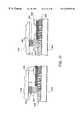
- FIGS. 1A and 1Bare cross-sectional views of a field off and a field on state, respectively, for a multi-domain vertically aligned liquid crystal display having color filter stacks and dams, spacer posts and pretilt structures (ridges) formed in a single lithographic process step in accordance with the present invention
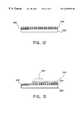
- FIG. 2is an illustrative pattern showing dams, spacers and pretilt structures formed in accordance with the present invention
- FIGS. 3-8are top views of liquid crystal displays showing a plurality of pretilt structures for trenches/ridges in accordance with the present invention
- FIGS. 9A and 9Bare cross-sectional views of a field off and a field on state, respectively, for a two-domain TN liquid crystal display having color filter stacks and dams, spacer posts and pretilt structures (ridges) formed in a single lithographic process step in accordance with the present invention
- FIGS. 10A and 10Bare cross-sectional views of a field off and a field on state, respectively, for a multi-domain vertically aligned liquid crystal display having color filter stacks and dams, spacer posts and pretilt structures (trenches) formed in a single lithographic process step in accordance with the present invention
- FIGS. 11A and 11Bare cross-sectional views of a field off and a field on state, respectively, for a two-domain TN liquid crystal display having color filter stacks and dams, spacer posts and pretilt structures (trenches) formed in a single lithographic process step in accordance with the present invention
- FIGS. 12-16are cross-sectional view of a liquid crystal display showing method steps for forming color filter stacks and concurrently forming dams, spacers and pretilt structures in a single lithographic process step in accordance with the present invention.
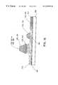
- FIG. 17is a cross-sectional view of a display device employing three color filter layers to provide a cell gap in accordance with the present invention.
- the present inventionrelates to liquid crystal displays, and more particularly to a display structure which provides improved performance and a method for fabricating pretilt structures, spacers and damns in a single lithographic step to decrease fabrication costs of the displays.
- the present inventionachieves dual goals of improving display performance and saving manufacturing costs by building post spacers, dams and liquid crystal molecule pretilt structures (e.g., ridges or slits) in one photolithographic mask step.
- a liquid crystal displayliquid crystal material is sandwiched between two substrates with a gap (cell gap) existing therebetween.
- Front of screen (FOS) quality of a displayis closely related to the accuracy of cell gap control.
- spacer ballsare used to control the cell gap of the LCD panel. The spacer balls are randomly sprayed on the surface of one substrate before the two substrates are assembled together. This method can control cell gap with the uncertainty in the range of ⁇ 0.5 ⁇ m.
- the random distribution of the spacer balls in the panelalso causes light leakage in the dark state. This results in a reduction of contrast ratio of the LCD due to light leakage around the spacer balls in the dark state.
- the present inventioneliminates spacer balls by employing post spacers.
- Post spacersare fabricated using, for example, polymer material which is the same as or similar to that of a color filter layer.
- a photolithographic processis used to build the post spacers away from pixel areas so that there are no spacers in the pixel area to cause light leakage in the dark state. Therefore, the contrast ratio of the LCD is much improved.
- the post spacershave better cell gap control, for example, two times more accurate than that of spacer balls.
- the post spacerscan be built on the TFT (thin-film-transistor) substrate or on the color filter substrate, or both.
- a glue sealis used to hold two substrates together and to confine liquid crystal material inside the glue seal pattern. Due to the possible interaction between the glue seal material and liquid crystal, the LCD panel may have FOS problems, such as white smearing, near the glue edge. Dam structures are preferably built around the inside edge of the glue area and outside of the display active area to prevent or reduce the FOS problems.
- the dam structuremay be built in accordance with the invention using the same material as or similar to that of color filter with the same photolithographic process.
- a multi-domain vertical alignment methodcan be used to improve the display viewing angle.
- An MVA structureis based on pretilt angle control using either a ridge, a slit or a combination of structures to form a fringe field.
- the ridge structuremay be built using the same material as or similar to that of color filter with the same photolithographic process. Therefore, by employing the present invention, a single lithographic process yields spacer posts, dam structures and pretilt structures and their associated advantages.
- FIG. 1Aa cross-sectional view of a liquid crystal display device 100 is shown.
- the panel structures of FIGS. 1A and 1Binclude a multi-domain vertical alignment (VA) liquid crystal display.
- FIG. 1Ashows an orientation of molecules of a liquid crystal material 101 in a field off (or low field) state
- FIG. 1Bshows an orientation of molecules of liquid crystal material 101 in a field on (or high field) state.
- Device 100includes a substrate 102 also known as a color filter substrate, and a substrate 104 also known as a transistor substrate or a thin film transistor (TFT) array substrate.
- TFTthin film transistor
- Substrate 102may include a black matrix layer (not shown) for reducing light leakage around pixels as is known in the art.
- a color filter layer 106preferably includes three color filters (red, green and blue color filters). Each color filter includes is patterned in a separate photolithographic step.
- the present inventionexploits the need for three filters and three process steps by overlapping the color filters in strategic locations to form at least a portion of post spacers 108 and at least a portion of dams 110 . In these areas, three color layers are overlapped to provide additional height on which dams 110 and post spacers 108 will be built.
- Color filter stacks 112are formed by employing modified lithographic patterns to create the appropriate over lap of the color filter layers.
- a layer 118is deposited over color filter layer 106 and color filter stacks 112 to form a transparent electrode 122 .
- Layer 118preferably includes a transparent conductor layer, such as, for example, indium tin oxide or indium zinc oxide.
- Next dams 110 , post spacers 108 and ridges 114are built by depositing a layer 120 on layer 118 over color filter layer 106 and color filter stacks 112 .
- layer 120is patterned using a single photo mask and photolithographic step.
- Layer 120preferably includes a dielectric material such as, for example, XP9595 available from Shipley, Inc., Optomer-NN500 commercially available from JSR, or CT-122, available from Fuji-Olin (layer 120 is transparent).
- a portion 130 of dam 110 , a portion 132 of post spacer 108 and pretilt structure 134are formed.
- the thickness of layer 120is about half of a cell gap (G) and color filter stacks 112 are formed such that the thickness of two the color filter layers is about half of the cell gap such that the sum of the two equals the cell gap distance (G).
- Substrate 104includes pixel electrodes 138 , thin film transistors (not shown) and other display circuitry.
- the present inventionmay form portions of spacer posts, dams and/or pretilt structures on substrate 104 or form these structures on a combination of substrate 102 and substrate 104 .
- Color filter substrate 102 and a corresponding TFT array substrate 104are then coated with a vertical alignment layer 105 , such as, for example, SE-1211 from Nissan Chemical, Inc., JALS688 from JSR Inc. or other dry deposition vertical alignment layers.
- a vertical alignment layer 105such as, for example, SE-1211 from Nissan Chemical, Inc., JALS688 from JSR Inc. or other dry deposition vertical alignment layers.
- no rubbing or other alignment treatmentis needed.
- Substrates 102 and 104are then assembled together using conventional LCD cell fabrication methods and preferably a negative dielectric anisotrpoic liquid crystal, such as, for example, MLL 2039 available from Merck, Inc. which is employed to fill gap (G) between the panels.
- cell gap thickness (G)is controlled by the sum of thickness of two (or three) color filter layers of color filter stack 112 and post spacer 108 .
- the thickness of the ridge of pretilt structure 134is about half of the cell gap.
- Dam 110is located next to a glue seal pattern 113 and is used to prevent glue interaction or contamination with liquid crystal, i.e. seal off the liquid crystal.
- Spacers 108are used which include color filter stacks 112 to control the cell gap of the display panel.
- Y-inverse-Y ridgesare pretilt control structures 134 for providing pretilt control to form multi-domains for each pixel in a display.
- Pretilt control structures 134(and pixel edges) are used to control the tilting direction of liquid crystal molecules and to widen display viewing angles. Different ridge or trench structures may be employed. Examples of these ridge or trench structures are given in FIGS.
- FIGS. 9A and 9Ba cross-sectional view of a liquid crystal display device 200 is shown.
- the panel cross-sectional structures of FIGS. 9A and 9Binclude a two-domain TN (twisted nematic) liquid crystal display.
- FIG. 9Ashows an orientation of molecules of a liquid crystal material 101 in a field off (or low field) state
- FIG. 9Bshows an orientation of molecules of liquid crystal material 101 in a field on (or high field) state.
- FIGS. 9A and 9BThe structure of FIGS. 9A and 9B is similar to that of FIGS. 1A and 1B; however a homogeneous (planar) alignment layer 107 with an almost zero pretilt angle is preferably employed.
- the almost zero pretilt homogenous alignmentcan be achieved by a polymer layer coating, similar to those described for layer 105 above, followed with polarizer UV alignment or by silicon oxide film coating followed by proper ion beam treatment.
- pretilt structures (ridges) 134 in combination with fringe field from the pixel edgeare used to control the tilting direction of liquid crystal molecules and to widen display viewing angles. Examples of the ridge or trench structures are given in FIGS. 3-8 and in U.S. Pat. No. 5,907,380.
- the color filter, post spacer, dam and ridgesare built on the color filter substrate. These layers can also be built on the TFT array substrate as described below.
- pretilt structures 134are replaced by pretilt structures 334 in the form of slits, preferably in a polymer layer, on TFT array substrate 304 for device 300 .
- a cell gap (G)is determined by the thickness of the sum of a color filter stack 312 and a layer 320 .
- a color filter layer 306includes three color filters (red, green and blue color filters). Each color filter includes is patterned in a separate photolithographic step.
- the present inventionexploits the need for three filters (although two or more layers can be overlapped) and three process steps by overlapping the color filters in strategic locations to form at least a portion of post spacers 308 and at least a portion of dams 310 . In these areas, three color layers are overlapped to provide additional height on which dams 310 and post spacers 308 will be built.
- Color filter stacks 312are formed by employing modified lithographic patterns to create the appropriate over lap of the color filter layers.
- a layer 318is deposited over color filter layer 306 and patterned to form pixel electrodes 322 .
- Layer 318preferably includes a transparent conductor layer, such as, for example, indium tin oxide or indium zinc oxide.
- Next dams 310 , post spacers 308 and trenches 314are built by depositing layer 320 on color filter layer 306 and color filter stacks 312 .
- layer 320is patterned using a single photo mask and photolithographic step.
- Layer 320preferably includes a dielectric material such as, for example, XP9595 available from Shipley, Inc., Optomer-NN500 commercially available from JSR, or CT-122, available from Fuji-Olin.
- a portion 330 of dam 310 , a portion 332 of post spacer 308 and pretilt structure 334are formed.
- the thickness of layer 320is about half of a cell gap (G) and color filter stacks 312 are formed such that the thickness of two the color filter layers is about half of the cell gap such that the sum of the two equals the cell gap distance (G).
- the cell gapis maintained by two or more color filter layers which include a total thickness equal to the cell gap distance (G).
- Substrate 302includes a common transparent electrode 338
- substrate 304includes thin film transistors (not shown) and other display circuitry.
- the present inventionmay form portions of spacer posts, dams and/or pretilt structures on substrate 304 or form these structures on a combination of substrate 302 and substrate 304 .
- Substrate 302 and a substrate 304are then coated with a vertical alignment layer 305 , such as, for example, SE-1211 from Nissan Chemical, Inc., JALS688 from JSR Inc. or other dry deposition vertical alignment layers.
- a vertical alignment layer 305such as, for example, SE-1211 from Nissan Chemical, Inc., JALS688 from JSR Inc. or other dry deposition vertical alignment layers.
- no rubbing or other alignment treatmentis needed.
- Substrates 102 and 104are then assembled together using conventional LCD cell fabrication methods and preferably a negative dielectric anisotropic liquid crystal material, for example, MLL 2039, available from Merck, Inc., is used to fill gap G.
- Layer 320may include a polymer, such as, for example, XP9595 available from Shipley, Inc., Optomer-NN500 commercially available from JSR, or CT-122, available from Fuji-Olin.
- Pretilt structures 334include the structures shown in FIGS. 3-8, and those described in U.S. Pat. No. 5,907,380 as slit or trench structures (i.e., slits instead of ridges).
- FIGS. 10A and 10Binclude a multi-domain vertically aligned (MVA) liquid crystal display.
- FIG. 10Ashows an orientation of molecules of a liquid crystal material 101 in a field off (or low field state
- FIG. 10Bshows an orientation of molecules of liquid crystal material 101 in a field on (or high field) state.
- a black matrix layeris omitted for simplicity in FIGS. 10A-B and 11 A-B.
- FIGS. 11A and 11Ba cross-sectional view of a liquid crystal display device 400 is shown.
- the panel cross-sectional structures of FIGS. 11A and 11Binclude a two-domain TN liquid crystal display.
- FIG. 11Ashows an orientation of molecules of a liquid crystal material 101 in a field off (or low field) state
- FIG. 11Bshows an orientation of molecules of liquid crystal material 101 in a field on (or high field) state.
- FIGS. 12-16an illustrative method is shown for forming color stacks 112 ( 312 ) (FIGS. 1A-B, 9 A-B or FIGS. 10A-B, 11 A-B) in accordance with the present invention.
- a first color filter layer 504is formed on a substrate 500 which may include a glass, plastic or quartz substrate.
- Substrate 500may include a black matrix layer 502 or other layers as needed.
- First color filter layer 504is deposited on substrate 500 .
- color filter layer 504is patterned to include an overlap region 508 .
- a second color filter 510is then deposited on color filter layer 504 .
- color filter layer 510is patterned also providing overlap in overlap region 508 .
- a third color filter layer 512is then deposited.
- color filter layer 512is patterned to form color filter stack 112 (or 312 ).
- a layer 120(or 320 ) is then deposited after an electrode layer 118 (or 318 ) and dams 110 (or 310 ), spacer posts 108 ( 308 ) and pretilt structures 134 (or 334 ) (not shown) are formed as shown in FIGS. 1A-B and 10 A-B, for example.
- dams 602 and/or post spacers 604may be employed to form dams 602 and/or post spacers 604 by providing sufficient thickness of the layers.
- Dams 602 and post spacers 604provide gap distance G between substrate 610 and 612 .
- pretilt control structures 606may be formed by employing the dielectric layer as described above.
- dams 602 , spacers 604 or pretilt control structures 606may be employed together or independently in accordance with the invention.
Landscapes
- Physics & Mathematics (AREA)
- Nonlinear Science (AREA)
- Mathematical Physics (AREA)
- Chemical & Material Sciences (AREA)
- Crystallography & Structural Chemistry (AREA)
- General Physics & Mathematics (AREA)
- Optics & Photonics (AREA)
- Liquid Crystal (AREA)
- Spectroscopy & Molecular Physics (AREA)
- Engineering & Computer Science (AREA)
- Microelectronics & Electronic Packaging (AREA)
Abstract
Description
Claims (25)
Priority Applications (4)
| Application Number | Priority Date | Filing Date | Title |
|---|---|---|---|
| US09/426,502US6493050B1 (en) | 1999-10-26 | 1999-10-26 | Wide viewing angle liquid crystal with ridge/slit pretilt, post spacer and dam structures and method for fabricating same |
| TW89121466ATW573151B (en) | 1999-10-26 | 2000-10-13 | Wide viewing angle liquid crystal with ridge/slit pretilt, post spacer and dam structures and method for fabricating same |
| CNB001314262ACN1152282C (en) | 1999-10-26 | 2000-10-18 | Liquid crystal display and method for forming functional structure thereof |
| KR10-2000-0061254AKR100421274B1 (en) | 1999-10-26 | 2000-10-18 | Wide viewing angle liquid crystal with ridge/slit pretilt, post spacer and dam structures and method for fabricating same |
Applications Claiming Priority (1)
| Application Number | Priority Date | Filing Date | Title |
|---|---|---|---|
| US09/426,502US6493050B1 (en) | 1999-10-26 | 1999-10-26 | Wide viewing angle liquid crystal with ridge/slit pretilt, post spacer and dam structures and method for fabricating same |
Publications (1)
| Publication Number | Publication Date |
|---|---|
| US6493050B1true US6493050B1 (en) | 2002-12-10 |
Family
ID=23691056
Family Applications (1)
| Application Number | Title | Priority Date | Filing Date |
|---|---|---|---|
| US09/426,502Expired - LifetimeUS6493050B1 (en) | 1999-10-26 | 1999-10-26 | Wide viewing angle liquid crystal with ridge/slit pretilt, post spacer and dam structures and method for fabricating same |
Country Status (4)
| Country | Link |
|---|---|
| US (1) | US6493050B1 (en) |
| KR (1) | KR100421274B1 (en) |
| CN (1) | CN1152282C (en) |
| TW (1) | TW573151B (en) |
Cited By (45)
| Publication number | Priority date | Publication date | Assignee | Title |
|---|---|---|---|---|
| US20010019389A1 (en)* | 1999-12-31 | 2001-09-06 | Lee Joun Ho | Multi-domain liquid crystal display device |
| US20020047971A1 (en)* | 2000-10-04 | 2002-04-25 | Lg.Philips Lcd Co., Ltd. | Multi-domain liquid crystal display and method for manufacturing the same |
| US20030011731A1 (en)* | 2001-04-04 | 2003-01-16 | Fujitsu Limited | Liquid crystal display device with retardation plates |
| US20030030769A1 (en)* | 2001-08-10 | 2003-02-13 | Hyung Ki Hong | Multi-domain liquid crystal display |
| US20030202143A1 (en)* | 1999-07-30 | 2003-10-30 | Fujitsu Display Technologies Corporation | Alignment films in a liquid crystal display device and a method of manufacturing the same |
| US20030202145A1 (en)* | 1998-12-25 | 2003-10-30 | Fujitsu Display Technologies Corporation | Multidomain vertically aligned liquid crystal display device |
| US6690441B2 (en)* | 2000-09-22 | 2004-02-10 | Dai Nippon Printing Co., Ltd. | Multi-domain vertical alignment mode liquid crystal display having spacers formed over zigzag like alignment-controlling projection |
| US20040114081A1 (en)* | 2001-06-29 | 2004-06-17 | Fujitsu Display Technologies Corporation | Substrate for liquid crystal display, liquid crystal display having the same and method of manufacturing the same |
| US20040239867A1 (en)* | 2003-05-29 | 2004-12-02 | Chi Mei Optoelectronics Corp. | Method for manufacturing liquid crystal display |
| US20040247973A1 (en)* | 2003-03-27 | 2004-12-09 | Sammes Nigel Mark | Methods of manufacture of electrolyte tubes for solid oxide devices and the devices obtained therefrom |
| US20050024567A1 (en)* | 2000-11-27 | 2005-02-03 | Fujitsu Display Technologies Corporation | Substrate for liquid crystal display device, manufacturing method of the same, and liquid crystal display device having the same |
| US20050062907A1 (en)* | 2003-09-22 | 2005-03-24 | Kohji Matsuoka | Liquid crystal display device |
| US20050099579A1 (en)* | 2003-11-10 | 2005-05-12 | Yoo Soon S. | Liquid crystal display panel and fabricating method thereof |
| US20050110939A1 (en)* | 2003-10-29 | 2005-05-26 | Seiko Epson Corporation | Liquid crystal display and electronic apparatus |
| US20050140892A1 (en)* | 2003-12-30 | 2005-06-30 | Lg.Philips Lcd Co., Ltd. | Liquid crystal display and fabricating method thereof |
| US20050206829A1 (en)* | 2004-03-16 | 2005-09-22 | Sharp Kabushiki Kaisha | Liquid crystal display device and its manufacturing method |
| US20060028598A1 (en)* | 2004-08-03 | 2006-02-09 | Samsung Electronics Co., Ltd. | Color filter panel, display panel having the same and method of manufacturing the same |
| US20060092366A1 (en)* | 1999-07-09 | 2006-05-04 | Hiroyasu Inoue | Liquid crystal display and method of fabricating the same |
| US20060158599A1 (en)* | 2005-01-18 | 2006-07-20 | Samsung Electronics Co., Ltd. | Color filter array panel and liquid crystal display including the same |
| US7102718B1 (en) | 2000-03-16 | 2006-09-05 | Semiconductor Energy Laboratory Co., Ltd. | Liquid crystal display device with particular TFT structure and method of manufacturing the same |
| US20060209245A1 (en)* | 2000-08-14 | 2006-09-21 | Joong-Hyun Mun | Liquid crystal display and a method for fabricating the same |
| US20070002263A1 (en)* | 2005-06-30 | 2007-01-04 | Lg.Philips Co., Ltd. | Liquid crystal display panel and method of fabricating the same |
| US20070146568A1 (en)* | 2000-03-17 | 2007-06-28 | Semiconductor Energy Laboratory Co., Ltd. | Liquid crystal display device and manufacturing method thereof |
| US20070195251A1 (en)* | 2006-02-22 | 2007-08-23 | Toppoly Optoelectronics Corp. | Systems for displaying images involving alignment liquid crystal displays |
| US20070195249A1 (en)* | 2000-11-22 | 2007-08-23 | Joong-Hyun Mun | Liquid crystal display having wide viewing angle |
| US20070206141A1 (en)* | 2006-03-01 | 2007-09-06 | Toppoly Optoelectronics Corp. | Vertical alignment liquid crystal displays |
| US20080284953A1 (en)* | 2007-05-18 | 2008-11-20 | Tpo Displays Corp. | Multi-domain vertical alignment liquid crystal display device |
| US20090008645A1 (en)* | 2007-07-06 | 2009-01-08 | Semiconductor Energy Laboratory Co., Ltd. | Light-emitting device |
| US20090316096A1 (en)* | 2000-06-20 | 2009-12-24 | Alessandro Cesare Callegari | Multi-domain and ips liquid-crystal display using dry alignment |
| US7652294B2 (en) | 2000-03-08 | 2010-01-26 | Semiconductor Energy Laboratory Co., Ltd. | Semiconductor device and manufacturing method thereof |
| US7687325B2 (en) | 2000-03-13 | 2010-03-30 | Semiconductor Energy Laboratory Co., Ltd. | Semiconductor device and manufacturing method thereof |
| US7697106B2 (en)* | 2000-01-14 | 2010-04-13 | Sharp Kabushiki Kaisha | Liquid crystal display device and method of manufacturing the same |
| US7705354B2 (en) | 2000-03-06 | 2010-04-27 | Semiconductor Energy Laboratory Co., Ltd | Semiconductor device and method for fabricating the same |
| US7714329B2 (en) | 2001-03-06 | 2010-05-11 | Semiconductor Energy Laboratory Co., Ltd. | Semiconductor device having thin film transistor |
| US20100155731A1 (en)* | 2008-12-24 | 2010-06-24 | Boe Technology Group Co., Ltd. | Touching-type electronic paper and method for manufacturing the same |
| US20100238391A1 (en)* | 2007-07-06 | 2010-09-23 | Semiconductor Energy Laboratory Co., Ltd. | Liquid crystal display device |
| US7902550B2 (en) | 2000-05-09 | 2011-03-08 | Semiconductor Energy Laboratory Co., Ltd. | Semiconductor device and manufacturing method thereof |
| US8093112B2 (en) | 2007-07-20 | 2012-01-10 | Semiconductor Energy Laboratory Co., Ltd. | Method for manufacturing display device |
| US8300201B2 (en) | 2000-03-13 | 2012-10-30 | Semiconductor Energy Laboratory Co., Ltd. | Semiconductor device and a method of manufacturing the same |
| CN102955287A (en)* | 2012-10-12 | 2013-03-06 | 华映视讯(吴江)有限公司 | Color filter substrate and display panel |
| US20140063420A1 (en)* | 2012-08-30 | 2014-03-06 | Chunghwa Picture Tubes, Ltd. | Color filter substrate and display panel |
| US8786929B2 (en) | 2002-06-10 | 2014-07-22 | E Ink Corporation | Components and methods for use in electro-optic displays |
| EP2980636A1 (en)* | 2014-07-30 | 2016-02-03 | Samsung Display Co., Ltd. | Liquid crystal display panel and manufacturing method thereof |
| US20160187685A1 (en)* | 2013-06-28 | 2016-06-30 | Boe Technology Group Co., Ltd. | Display panel and its manufacturing method and a display |
| US20180052343A1 (en)* | 2015-08-26 | 2018-02-22 | Shenzhen China Star Optoelectronics Technology Co. Ltd. | Array substrate and display device |
Families Citing this family (8)
| Publication number | Priority date | Publication date | Assignee | Title |
|---|---|---|---|---|
| KR100746283B1 (en)* | 2002-01-25 | 2007-08-03 | 삼성전자주식회사 | LCD Display |
| KR101009668B1 (en)* | 2003-10-06 | 2011-01-19 | 엘지디스플레이 주식회사 | LCD and its manufacturing method |
| CN100376960C (en)* | 2004-03-02 | 2008-03-26 | 鸿富锦精密工业(深圳)有限公司 | Multiple-domain vertical orientation type liquid crystal display device |
| JP3891995B2 (en)* | 2004-04-26 | 2007-03-14 | シャープ株式会社 | Liquid crystal display |
| CN100356246C (en)* | 2005-01-28 | 2007-12-19 | 友达光电股份有限公司 | Liquid crystal display panel and manufacturing method thereof |
| US20090185128A1 (en)* | 2008-01-23 | 2009-07-23 | Himax Display, Inc. | Active device array substrate, common electrode substrate, and reflective type liquid crystal panel |
| TWI414973B (en) | 2008-09-19 | 2013-11-11 | Asustek Comp Inc | Portable computer and touch input device |
| CN102566127A (en)* | 2012-02-06 | 2012-07-11 | 深圳市瑞福达液晶显示技术股份有限公司 | Forming method for liquid crystal cell for 3D (three-dimensional) liquid crystal glasses |
Citations (9)
| Publication number | Priority date | Publication date | Assignee | Title |
|---|---|---|---|---|
| US5680187A (en)* | 1994-04-04 | 1997-10-21 | International Business Machines Corporation | Liquid crystal display device and method for manufacturing the same |
| US5748266A (en)* | 1995-03-10 | 1998-05-05 | International Business Machines Corporation | Color filter, liquid crystal display panel, liquid crystal display, and liquid crystal display panel manufacturing method |
| US5757451A (en)* | 1995-09-08 | 1998-05-26 | Kabushiki Kaisha Toshiba | Liquid crystal display device spacers formed from stacked color layers |
| US5815232A (en)* | 1995-08-18 | 1998-09-29 | Kabushiki Kaisha Toshiba | Color liquid crystal display apparatus |
| US5831710A (en) | 1997-02-06 | 1998-11-03 | International Business Machines Corporation | Liquid crystal display |
| US5907380A (en) | 1997-10-30 | 1999-05-25 | International Business Machines Corporation | Liquid crystal cell employing thin wall for pre-tilt control |
| US6010384A (en)* | 1997-08-29 | 2000-01-04 | Kabushiki Kaisha Toshiba | Liquid crystal display device and method for manufacturing the same |
| US6256080B1 (en)* | 1999-06-23 | 2001-07-03 | International Business Machines Corporation | Self-aligned structures for improved wide viewing angle for liquid crystal displays |
| US6281960B1 (en)* | 1998-02-27 | 2001-08-28 | Sharp Kabushiki Kaisha | LCD with black matrix wall(s) |
Family Cites Families (5)
| Publication number | Priority date | Publication date | Assignee | Title |
|---|---|---|---|---|
| JPH0915643A (en)* | 1995-07-03 | 1997-01-17 | Fujitsu Ltd | LCD panel |
| JPH09120074A (en)* | 1995-08-18 | 1997-05-06 | Toshiba Electron Eng Corp | Color filter substrate and liquid crystal display device using the same |
| JPH10221696A (en)* | 1997-02-06 | 1998-08-21 | Toppan Printing Co Ltd | Color filter for liquid crystal display device, method of manufacturing the same, and liquid crystal display device |
| JPH10253967A (en)* | 1997-03-07 | 1998-09-25 | Toshiba Electron Eng Corp | Liquid crystal display |
| JPH11212075A (en)* | 1998-01-23 | 1999-08-06 | Toshiba Electronic Engineering Corp | Manufacturing method of liquid crystal display device |
- 1999
- 1999-10-26USUS09/426,502patent/US6493050B1/ennot_activeExpired - Lifetime
- 2000
- 2000-10-13TWTW89121466Apatent/TW573151B/ennot_activeIP Right Cessation
- 2000-10-18KRKR10-2000-0061254Apatent/KR100421274B1/ennot_activeExpired - Lifetime
- 2000-10-18CNCNB001314262Apatent/CN1152282C/ennot_activeExpired - Lifetime
Patent Citations (9)
| Publication number | Priority date | Publication date | Assignee | Title |
|---|---|---|---|---|
| US5680187A (en)* | 1994-04-04 | 1997-10-21 | International Business Machines Corporation | Liquid crystal display device and method for manufacturing the same |
| US5748266A (en)* | 1995-03-10 | 1998-05-05 | International Business Machines Corporation | Color filter, liquid crystal display panel, liquid crystal display, and liquid crystal display panel manufacturing method |
| US5815232A (en)* | 1995-08-18 | 1998-09-29 | Kabushiki Kaisha Toshiba | Color liquid crystal display apparatus |
| US5757451A (en)* | 1995-09-08 | 1998-05-26 | Kabushiki Kaisha Toshiba | Liquid crystal display device spacers formed from stacked color layers |
| US5831710A (en) | 1997-02-06 | 1998-11-03 | International Business Machines Corporation | Liquid crystal display |
| US6010384A (en)* | 1997-08-29 | 2000-01-04 | Kabushiki Kaisha Toshiba | Liquid crystal display device and method for manufacturing the same |
| US5907380A (en) | 1997-10-30 | 1999-05-25 | International Business Machines Corporation | Liquid crystal cell employing thin wall for pre-tilt control |
| US6281960B1 (en)* | 1998-02-27 | 2001-08-28 | Sharp Kabushiki Kaisha | LCD with black matrix wall(s) |
| US6256080B1 (en)* | 1999-06-23 | 2001-07-03 | International Business Machines Corporation | Self-aligned structures for improved wide viewing angle for liquid crystal displays |
Non-Patent Citations (1)
| Title |
|---|
| Takeda et al., "41.1: A Super-High-Image-Quality Multi-Domain Vertical Alignment LCD by New Rubbing-Less Technology", May 1998, SID '98 Digest, pp. 1077-1080.* |
Cited By (145)
| Publication number | Priority date | Publication date | Assignee | Title |
|---|---|---|---|---|
| US6882393B2 (en)* | 1998-12-25 | 2005-04-19 | Fujitsu Display Technologies Corporation | Multidomain vertically aligned liquid crystal display device |
| US20030202145A1 (en)* | 1998-12-25 | 2003-10-30 | Fujitsu Display Technologies Corporation | Multidomain vertically aligned liquid crystal display device |
| US7423718B2 (en) | 1999-07-09 | 2008-09-09 | Sharp Kabushiki Kaisha | Liquid crystal display comprising protrusion structure having same material, same layer but lower height than pillar-shaped spacer |
| US7330220B2 (en) | 1999-07-09 | 2008-02-12 | Sharp Kabushiki Kaisha | Liquid crystal display and method of fabricating the same |
| US20070258026A1 (en)* | 1999-07-09 | 2007-11-08 | Kazuhiko Sumi | Liquid crystal display and method of fabricating the same |
| US7259825B2 (en)* | 1999-07-09 | 2007-08-21 | Sharp Kabushiki Kaisha | Liquid crystal display and method of fabricating the same comprising simultaneously forming pillar-shaped spacer and protrusion structure |
| US20060098151A1 (en)* | 1999-07-09 | 2006-05-11 | Hiroyasu Inoue | Liquid crystal display and method of fabricating the same |
| US20060092366A1 (en)* | 1999-07-09 | 2006-05-04 | Hiroyasu Inoue | Liquid crystal display and method of fabricating the same |
| US7859624B2 (en) | 1999-07-30 | 2010-12-28 | Sharp Kabushiki Kaisha | Alignment films in a liquid crystal display device with polymer mixture and a method of manufacturing the same |
| US20070273818A1 (en)* | 1999-07-30 | 2007-11-29 | Hidefumi Yoshida | Alignment films in a liquid crystal display device and a method of manufacturing the same |
| US20030202143A1 (en)* | 1999-07-30 | 2003-10-30 | Fujitsu Display Technologies Corporation | Alignment films in a liquid crystal display device and a method of manufacturing the same |
| US8416379B2 (en) | 1999-07-30 | 2013-04-09 | Sharp Kabushiki Kaisha | Alignment films in a liquid crystal display device and a method of manufacturing the same |
| US6850300B2 (en)* | 1999-12-31 | 2005-02-01 | Lg Philips Lcd Co., Ltd. | Multi-domain liquid crystal display device with particular dielectric frames |
| US20010019389A1 (en)* | 1999-12-31 | 2001-09-06 | Lee Joun Ho | Multi-domain liquid crystal display device |
| US7697106B2 (en)* | 2000-01-14 | 2010-04-13 | Sharp Kabushiki Kaisha | Liquid crystal display device and method of manufacturing the same |
| US9099355B2 (en) | 2000-03-06 | 2015-08-04 | Semiconductor Energy Laboratory Co., Ltd. | Semiconductor device and method of fabricating the same |
| US7705354B2 (en) | 2000-03-06 | 2010-04-27 | Semiconductor Energy Laboratory Co., Ltd | Semiconductor device and method for fabricating the same |
| US7973312B2 (en) | 2000-03-06 | 2011-07-05 | Semiconductor Energy Laboratory Co., Ltd. | Semiconductor device and method of fabricating the same |
| US8188478B2 (en) | 2000-03-06 | 2012-05-29 | Semiconductor Energy Laboratory Co., Ltd. | Semiconductor device and method of fabricating the same |
| US7728334B2 (en) | 2000-03-08 | 2010-06-01 | Semiconductor Energy Laboratory Co., Ltd. | Semiconductor device and manufacturing method thereof |
| US9368514B2 (en) | 2000-03-08 | 2016-06-14 | Semiconductor Energy Laboratory Co., Ltd. | Semiconductor device and manufacturing method thereof |
| US9786687B2 (en) | 2000-03-08 | 2017-10-10 | Semiconductor Energy Laboratory Co., Ltd. | Semiconductor device and manufacturing method thereof |
| US7652294B2 (en) | 2000-03-08 | 2010-01-26 | Semiconductor Energy Laboratory Co., Ltd. | Semiconductor device and manufacturing method thereof |
| US9059045B2 (en) | 2000-03-08 | 2015-06-16 | Semiconductor Energy Laboratory Co., Ltd. | Semiconductor device and manufacturing method thereof |
| US8586988B2 (en) | 2000-03-08 | 2013-11-19 | Semiconductor Energy Laboratory Co., Ltd. | Semiconductor device and manufacturing method thereof |
| US8198630B2 (en) | 2000-03-08 | 2012-06-12 | Semiconductor Energy Laboratory Co., Ltd. | Semiconductor device and manufacturing method thereof |
| US7687325B2 (en) | 2000-03-13 | 2010-03-30 | Semiconductor Energy Laboratory Co., Ltd. | Semiconductor device and manufacturing method thereof |
| US8934066B2 (en) | 2000-03-13 | 2015-01-13 | Semiconductor Energy Laboratory Co., Ltd. | Semiconductor device having stick drivers and a method of manufacturing the same |
| US8300201B2 (en) | 2000-03-13 | 2012-10-30 | Semiconductor Energy Laboratory Co., Ltd. | Semiconductor device and a method of manufacturing the same |
| US7990508B2 (en) | 2000-03-16 | 2011-08-02 | Semiconductor Energy Laboratory Co., Ltd. | Liquid crystal display device and method of manufacturing the same |
| US8228477B2 (en) | 2000-03-16 | 2012-07-24 | Semiconductor Energy Laboratory Co., Ltd. | Liquid crystal display device and method of manufacturing the same |
| US8610861B2 (en) | 2000-03-16 | 2013-12-17 | Semiconductor Energy Laboratory Co., Ltd. | Liquid crystal display device and method of manufacturing the same |
| US9298056B2 (en) | 2000-03-16 | 2016-03-29 | Semiconductor Energy Laboratory Co., Ltd. | Liquid crystal display device and method of manufacturing the same |
| US7656491B2 (en) | 2000-03-16 | 2010-02-02 | Semiconductor Energy Laboratory Co., Ltd. | Liquid crystal display device and method of manufacturing the same |
| US7102718B1 (en) | 2000-03-16 | 2006-09-05 | Semiconductor Energy Laboratory Co., Ltd. | Liquid crystal display device with particular TFT structure and method of manufacturing the same |
| US8873011B2 (en) | 2000-03-16 | 2014-10-28 | Semiconductor Energy Laboratory Co., Ltd. | Liquid crystal display device and method of manufacturing the same |
| US20070146568A1 (en)* | 2000-03-17 | 2007-06-28 | Semiconductor Energy Laboratory Co., Ltd. | Liquid crystal display device and manufacturing method thereof |
| US7714975B1 (en)* | 2000-03-17 | 2010-05-11 | Semiconductor Energy Laboratory Co., Ltd | Liquid crystal display device and manfacturing method thereof |
| US8421985B2 (en) | 2000-03-17 | 2013-04-16 | Semiconductor Energy Laboratory Co., Ltd. | Liquid crystal display device and manufacturing method thereof |
| US8558983B2 (en) | 2000-03-17 | 2013-10-15 | Semiconductor Energy Laboratory Co., Ltd. | Liquid crystal display device and manufacturing method thereof |
| US7902550B2 (en) | 2000-05-09 | 2011-03-08 | Semiconductor Energy Laboratory Co., Ltd. | Semiconductor device and manufacturing method thereof |
| US9429807B2 (en) | 2000-05-09 | 2016-08-30 | Semiconductor Energy Laboratory Co., Ltd. | Semiconductor device and manufacturing method thereof |
| US8823004B2 (en) | 2000-05-09 | 2014-09-02 | Semiconductor Energy Laboratory Co., Ltd. | Semiconductor device and manufacturing method thereof |
| US9048146B2 (en) | 2000-05-09 | 2015-06-02 | Semiconductor Energy Laboratory Co., Ltd. | Semiconductor device and manufacturing method thereof |
| US8525173B2 (en) | 2000-05-09 | 2013-09-03 | Semiconductor Energy Laboratory Co., Ltd. | Semiconductor device and manufacturing method thereof |
| US20090316096A1 (en)* | 2000-06-20 | 2009-12-24 | Alessandro Cesare Callegari | Multi-domain and ips liquid-crystal display using dry alignment |
| US7843542B2 (en) | 2000-08-14 | 2010-11-30 | Samsung Electronics Co., Ltd. | Liquid crystal display including a spacer element and method for fabricating the same |
| US8009257B2 (en) | 2000-08-14 | 2011-08-30 | Samsung Electronics Co., Ltd. | Liquid crystal display including a spacer and passivation formed of the same material |
| US8599354B2 (en) | 2000-08-14 | 2013-12-03 | Samsung Display Co., Ltd. | Liquid crystal display including a variable width spacer element |
| US20080284964A1 (en)* | 2000-08-14 | 2008-11-20 | Joong-Hyun Mun | Liquid crystal display and a method for fabricating the same |
| US7486364B2 (en) | 2000-08-14 | 2009-02-03 | Samsung Electronics Co., Ltd. | Liquid crystal display and a method for fabricating the same |
| US7525621B2 (en) | 2000-08-14 | 2009-04-28 | Samsung Electronics, Co., Ltd. | Liquid crystal display and a method for fabricating the same |
| US9577103B2 (en) | 2000-08-14 | 2017-02-21 | Samsung Display Co., Ltd. | Liquid crystal display including a variable width spacer element and method for fabricating the same |
| US8319929B2 (en) | 2000-08-14 | 2012-11-27 | Samsung Display Co., Ltd. | Liquid crystal display including a variable width spacer element and method for fabricating the same |
| US20060209245A1 (en)* | 2000-08-14 | 2006-09-21 | Joong-Hyun Mun | Liquid crystal display and a method for fabricating the same |
| US20070263163A1 (en)* | 2000-08-14 | 2007-11-15 | Samsung Electronics Co., Ltd. | Liquid crystal display and a method for fabricating the same |
| US7639337B2 (en) | 2000-08-14 | 2009-12-29 | Samsung Electronics Co., Ltd. | Liquid crystal display and method for fabricating the same |
| US7830492B2 (en) | 2000-08-14 | 2010-11-09 | Samsung Electronics Co., Ltd. | Liquid crystal display and method for fabricating the same |
| US20110037933A1 (en)* | 2000-08-14 | 2011-02-17 | Samsung Electronics Co., Ltd. | Liquid crystal display including a spacer element and method for fabricating the same |
| US20100053485A1 (en)* | 2000-08-14 | 2010-03-04 | Joong-Hyun Mun | Liquid crystal display and method for fabricating the same |
| US6690441B2 (en)* | 2000-09-22 | 2004-02-10 | Dai Nippon Printing Co., Ltd. | Multi-domain vertical alignment mode liquid crystal display having spacers formed over zigzag like alignment-controlling projection |
| US7365817B2 (en)* | 2000-10-04 | 2008-04-29 | Lg.Philips Lcd Co., Ltd. | Multi-domain liquid crystal display and method for manufacturing the same |
| US20020047971A1 (en)* | 2000-10-04 | 2002-04-25 | Lg.Philips Lcd Co., Ltd. | Multi-domain liquid crystal display and method for manufacturing the same |
| US20070195249A1 (en)* | 2000-11-22 | 2007-08-23 | Joong-Hyun Mun | Liquid crystal display having wide viewing angle |
| US7564526B2 (en) | 2000-11-22 | 2009-07-21 | Samsung Electronics Co., Ltd. | Liquid crystal display having wide viewing angle |
| US7426009B2 (en) | 2000-11-27 | 2008-09-16 | Sharp Kabushiki Kaisha | Substrate for liquid crystal display device, manufacturing method of the same, and liquid crystal display device having the same |
| US20070258025A1 (en)* | 2000-11-27 | 2007-11-08 | Manabu Sawasaki | Substrate for liquid crystal display device, manufacturing method of the same, and liquid crystal display device having the same |
| US20050024567A1 (en)* | 2000-11-27 | 2005-02-03 | Fujitsu Display Technologies Corporation | Substrate for liquid crystal display device, manufacturing method of the same, and liquid crystal display device having the same |
| US7245345B2 (en) | 2000-11-27 | 2007-07-17 | Sharp Kabushiki Kaisha | Substrate for liquid crystal display device, manufacturing method of the same, and liquid crystal display device having the same |
| US7875886B2 (en) | 2001-03-06 | 2011-01-25 | Semiconductor Energy Laboratory Co., Ltd. | Semiconductor device having a thin film transistor |
| US8053781B2 (en) | 2001-03-06 | 2011-11-08 | Semiconductor Energy Laboratory Co., Ltd. | Semiconductor device having thin film transistor |
| US7714329B2 (en) | 2001-03-06 | 2010-05-11 | Semiconductor Energy Laboratory Co., Ltd. | Semiconductor device having thin film transistor |
| US8461596B2 (en) | 2001-03-06 | 2013-06-11 | Semiconductor Energy Laboratory Co., Ltd. | Semiconductor device including semiconductor film with outer end having tapered shape |
| US20040095536A1 (en)* | 2001-04-04 | 2004-05-20 | Fujitsu Limited | Liquid crystal display device with retardation plates |
| US7151582B2 (en)* | 2001-04-04 | 2006-12-19 | Sharp Kabushiki Kaisha | Liquid crystal display device with negative retardation of retardation plates being approximately zero. |
| US7450205B2 (en) | 2001-04-04 | 2008-11-11 | Sharp Kabushiki Kaisha | Liquid crystal display device with retardation plates |
| US20030011731A1 (en)* | 2001-04-04 | 2003-01-16 | Fujitsu Limited | Liquid crystal display device with retardation plates |
| US7826027B2 (en)* | 2001-06-29 | 2010-11-02 | Sharp Kabushiki Kaisha | Substrate for liquid crystal display, liquid crystal display having the same and method of manufacturing the same |
| US8228473B2 (en) | 2001-06-29 | 2012-07-24 | Sharp Kabushiki Kaisha | Substrate for liquid crystal display, liquid crystal display having the same and method of manufacturing the same |
| US8493534B2 (en) | 2001-06-29 | 2013-07-23 | Sharp Kabushiki Kaisha | Substrate for liquid crystal display, liquid crystal display having the same and method of manufacturing the same |
| US9069221B2 (en) | 2001-06-29 | 2015-06-30 | Sharp Kabushiki Kaisha | Liquid crystal display device |
| US20040114081A1 (en)* | 2001-06-29 | 2004-06-17 | Fujitsu Display Technologies Corporation | Substrate for liquid crystal display, liquid crystal display having the same and method of manufacturing the same |
| US7215396B2 (en)* | 2001-08-10 | 2007-05-08 | Lg.Philips Lcd Co., Ltd. | Multi-domain liquid crystal display having spacer aligned with alignment boundary |
| US20030030769A1 (en)* | 2001-08-10 | 2003-02-13 | Hyung Ki Hong | Multi-domain liquid crystal display |
| US11294255B2 (en) | 2002-06-10 | 2022-04-05 | E Ink Corporation | Components and methods for use in electro-optic displays |
| US9733540B2 (en) | 2002-06-10 | 2017-08-15 | E Ink Corporation | Components and methods for use in electro-optic displays |
| US8786929B2 (en) | 2002-06-10 | 2014-07-22 | E Ink Corporation | Components and methods for use in electro-optic displays |
| US9563099B2 (en) | 2002-06-10 | 2017-02-07 | E Ink Corporation | Components and methods for use in electro-optic displays |
| US9778536B2 (en) | 2002-06-10 | 2017-10-03 | E Ink Corporation | Components and methods for use in electro-optic displays |
| US20040247973A1 (en)* | 2003-03-27 | 2004-12-09 | Sammes Nigel Mark | Methods of manufacture of electrolyte tubes for solid oxide devices and the devices obtained therefrom |
| US20040239867A1 (en)* | 2003-05-29 | 2004-12-02 | Chi Mei Optoelectronics Corp. | Method for manufacturing liquid crystal display |
| US20050062907A1 (en)* | 2003-09-22 | 2005-03-24 | Kohji Matsuoka | Liquid crystal display device |
| US20050110939A1 (en)* | 2003-10-29 | 2005-05-26 | Seiko Epson Corporation | Liquid crystal display and electronic apparatus |
| US7345726B2 (en)* | 2003-10-29 | 2008-03-18 | Seiko Epson Corporation | Liquid crystal display and electronic apparatus having dielectric structures and colorant layers |
| US20050099579A1 (en)* | 2003-11-10 | 2005-05-12 | Yoo Soon S. | Liquid crystal display panel and fabricating method thereof |
| US7206057B2 (en)* | 2003-11-10 | 2007-04-17 | Lg.Philips Lcd Co., Ltd. | Liquid crystal display panel and fabricating method thereof |
| US7470932B2 (en)* | 2003-11-10 | 2008-12-30 | Lg Display Co., Ltd. | Liquid crystal display panel and fabricating method thereof |
| US7633595B2 (en)* | 2003-12-30 | 2009-12-15 | Lg Display Co., Ltd. | Liquid crystal display panel having dummy color filter and fabricating method thereof |
| US20050140892A1 (en)* | 2003-12-30 | 2005-06-30 | Lg.Philips Lcd Co., Ltd. | Liquid crystal display and fabricating method thereof |
| US20050206829A1 (en)* | 2004-03-16 | 2005-09-22 | Sharp Kabushiki Kaisha | Liquid crystal display device and its manufacturing method |
| US7920243B2 (en)* | 2004-08-03 | 2011-04-05 | Samsung Electronics Co., Ltd. | Liquid crystal display having cell gap maintaining members located in the switching element region and the storage line region |
| US20060028598A1 (en)* | 2004-08-03 | 2006-02-09 | Samsung Electronics Co., Ltd. | Color filter panel, display panel having the same and method of manufacturing the same |
| US20060158599A1 (en)* | 2005-01-18 | 2006-07-20 | Samsung Electronics Co., Ltd. | Color filter array panel and liquid crystal display including the same |
| US7821612B2 (en)* | 2005-01-18 | 2010-10-26 | Samsung Electronics Co., Ltd. | Color filter array panel and liquid crystal display including the same |
| US20070002263A1 (en)* | 2005-06-30 | 2007-01-04 | Lg.Philips Co., Ltd. | Liquid crystal display panel and method of fabricating the same |
| US8081286B2 (en) | 2005-06-30 | 2011-12-20 | Lg Display Co., Ltd. | Liquid crystal display device having first column spacer corresponds to a TFT and a second column spacer corresponds to a storage capacitor |
| US20090135361A1 (en)* | 2006-02-22 | 2009-05-28 | Ruibo Lu | Systems for Displaying Images Involving Alignment Liquid Crystal Displays |
| US20070195251A1 (en)* | 2006-02-22 | 2007-08-23 | Toppoly Optoelectronics Corp. | Systems for displaying images involving alignment liquid crystal displays |
| US7450208B2 (en) | 2006-03-01 | 2008-11-11 | Tpo Displays Corp. | Vertical alignment liquid crystal displays |
| US20070206141A1 (en)* | 2006-03-01 | 2007-09-06 | Toppoly Optoelectronics Corp. | Vertical alignment liquid crystal displays |
| US20080284953A1 (en)* | 2007-05-18 | 2008-11-20 | Tpo Displays Corp. | Multi-domain vertical alignment liquid crystal display device |
| US7924383B2 (en) | 2007-05-18 | 2011-04-12 | Chimei Innolux Corporation | Multi-domain vertical alignment liquid crystal display device |
| US9188825B2 (en) | 2007-07-06 | 2015-11-17 | Semiconductor Energy Laboratory Co., Ltd. | Liquid crystal display device |
| US20090008645A1 (en)* | 2007-07-06 | 2009-01-08 | Semiconductor Energy Laboratory Co., Ltd. | Light-emitting device |
| US10678107B2 (en) | 2007-07-06 | 2020-06-09 | Semiconductor Energy Laboratory Co., Ltd. | Liquid crystal display device |
| US8111362B2 (en) | 2007-07-06 | 2012-02-07 | Semiconductor Energy Laboratory Co., Ltd. | Liquid crystal display device |
| US10712625B2 (en) | 2007-07-06 | 2020-07-14 | Semiconductor Energy Laboratory Co., Ltd. | Liquid crystal display device |
| US8325285B2 (en) | 2007-07-06 | 2012-12-04 | Semiconductor Energy Laboratory Co., Ltd. | Liquid crystal display device |
| US8842230B2 (en) | 2007-07-06 | 2014-09-23 | Semiconductor Energy Laboratory Co., Ltd. | Liquid crystal display device |
| US10338447B2 (en) | 2007-07-06 | 2019-07-02 | Semiconductor Energy Laboratory Co., Ltd. | Liquid crystal display device |
| US12066730B2 (en) | 2007-07-06 | 2024-08-20 | Semiconductor Energy Laboratory Co., Ltd. | Liquid crystal display device |
| US8334537B2 (en) | 2007-07-06 | 2012-12-18 | Semiconductor Energy Laboratory Co., Ltd. | Light-emitting device |
| US11194207B2 (en) | 2007-07-06 | 2021-12-07 | Semiconductor Energy Laboratory Co., Ltd. | Liquid crystal display device |
| US8462286B2 (en) | 2007-07-06 | 2013-06-11 | Semiconductor Energy Laboratory Co., Ltd. | Liquid crystal display device |
| US9766526B2 (en) | 2007-07-06 | 2017-09-19 | Semiconductor Energy Laboratory Co., Ltd. | Liquid crystal display device |
| US20100238391A1 (en)* | 2007-07-06 | 2010-09-23 | Semiconductor Energy Laboratory Co., Ltd. | Liquid crystal display device |
| US11726378B2 (en) | 2007-07-06 | 2023-08-15 | Semiconductor Energy Laboratory Co., Ltd. | Liquid crystal display device |
| US8093112B2 (en) | 2007-07-20 | 2012-01-10 | Semiconductor Energy Laboratory Co., Ltd. | Method for manufacturing display device |
| US20100155731A1 (en)* | 2008-12-24 | 2010-06-24 | Boe Technology Group Co., Ltd. | Touching-type electronic paper and method for manufacturing the same |
| US8569758B2 (en)* | 2008-12-24 | 2013-10-29 | Boe Technology Group Co., Ltd. | Touching-type electronic paper and method for manufacturing the same |
| US8940560B2 (en) | 2008-12-24 | 2015-01-27 | Boe Technology Group Co., Ltd. | Method for manufacturing touching-type electronic paper |
| US8743336B2 (en)* | 2012-08-30 | 2014-06-03 | Chunghwa Picture Tubes, Ltd. | Color filter substrate and display panel |
| US20140063420A1 (en)* | 2012-08-30 | 2014-03-06 | Chunghwa Picture Tubes, Ltd. | Color filter substrate and display panel |
| TWI449969B (en)* | 2012-08-30 | 2014-08-21 | Chunghwa Picture Tubes Ltd | Color filter substrate and display panel |
| CN102955287B (en)* | 2012-10-12 | 2014-12-10 | 华映视讯(吴江)有限公司 | Color filter substrate and display panel |
| CN102955287A (en)* | 2012-10-12 | 2013-03-06 | 华映视讯(吴江)有限公司 | Color filter substrate and display panel |
| US20160187685A1 (en)* | 2013-06-28 | 2016-06-30 | Boe Technology Group Co., Ltd. | Display panel and its manufacturing method and a display |
| US9588378B2 (en)* | 2013-06-28 | 2017-03-07 | Boe Technology Group Co., Ltd. | Display panel and its manufacturing method and a display |
| US10261358B2 (en) | 2014-07-30 | 2019-04-16 | Samsung Display Co., Ltd. | Liquid crystal display panel and manufacturing method thereof |
| US20180081237A1 (en) | 2014-07-30 | 2018-03-22 | Samsung Display Co., Ltd. | Liquid crystal display panel and manufacturing method thereof |
| EP3690529A1 (en)* | 2014-07-30 | 2020-08-05 | Samsung Display Co., Ltd. | Liquid crystal display panel |
| US9851600B2 (en) | 2014-07-30 | 2017-12-26 | Samsung Display Co., Ltd. | Liquid crystal display panel and manufacturing method thereof |
| US9632351B2 (en) | 2014-07-30 | 2017-04-25 | Samsung Display Co., Ltd. | Liquid crystal display panel and manufacturing method thereof |
| EP2980636A1 (en)* | 2014-07-30 | 2016-02-03 | Samsung Display Co., Ltd. | Liquid crystal display panel and manufacturing method thereof |
| US20180052343A1 (en)* | 2015-08-26 | 2018-02-22 | Shenzhen China Star Optoelectronics Technology Co. Ltd. | Array substrate and display device |
Also Published As
| Publication number | Publication date |
|---|---|
| KR20010040120A (en) | 2001-05-15 |
| CN1152282C (en) | 2004-06-02 |
| KR100421274B1 (en) | 2004-03-11 |
| TW573151B (en) | 2004-01-21 |
| CN1294310A (en) | 2001-05-09 |
Similar Documents
| Publication | Publication Date | Title |
|---|---|---|
| US6493050B1 (en) | Wide viewing angle liquid crystal with ridge/slit pretilt, post spacer and dam structures and method for fabricating same | |
| US7542120B2 (en) | Vertical alignment active matrix liquid crystal display device having particular transparent step films | |
| US5907380A (en) | Liquid crystal cell employing thin wall for pre-tilt control | |
| US6400440B1 (en) | Passive liquid crystal display having pre-tilt control structure and light absorbent material at a center | |
| US6678031B2 (en) | Liquid crystal display with protrusion patterns | |
| US7936431B2 (en) | Liquid crystal display having subpixels per color pixel | |
| US7193672B2 (en) | Liquid crystal display device and thin film transistor substrate | |
| JP3492582B2 (en) | Liquid crystal display device and method of manufacturing the same | |
| US6961107B2 (en) | Transflective display device with different pretilt angles and fabrication method for thereof | |
| US20070146600A1 (en) | Liquid crystal display and panel therefor | |
| KR100781477B1 (en) | Liquid crystal display device | |
| US8300192B2 (en) | Liquid crystal display and thin film transistor array panel usable with the liquid crystal display | |
| US20060044501A1 (en) | Vertical alignment active matrix liquid crystal display device | |
| US20050140867A1 (en) | Trans-reflecting type in plane switching mode liquid crystal display device having ferroelectric liquid crystal alignment layer | |
| US20060066791A1 (en) | Vertical alignment active matrix liquid crystal display device | |
| US20060255337A1 (en) | Multi-domain member for a display device | |
| EP1480070A2 (en) | LCD - TFT array with electrode cutouts for multi-domain pixels | |
| CN113631997A (en) | Liquid crystal panel and display device | |
| JPH0643462A (en) | Electric field control double refraction effect type liquid crystal display device | |
| JP4586696B2 (en) | Liquid crystal display element | |
| JP4629161B2 (en) | Liquid crystal display device | |
| JP2565639C (en) |
Legal Events
| Date | Code | Title | Description |
|---|---|---|---|
| AS | Assignment | Owner name:INTERNATIONAL BUSINESS MACHINES CORPORATION, NEW Y Free format text:ASSIGNMENT OF ASSIGNORS INTEREST;ASSIGNORS:LIEN, SHUI-CHIH A.;ODAHARA, SHUHICHI;SAITOH. YUKITO;REEL/FRAME:010448/0257;SIGNING DATES FROM 19991123 TO 19991129 | |
| STCF | Information on status: patent grant | Free format text:PATENTED CASE | |
| FEPP | Fee payment procedure | Free format text:PAYOR NUMBER ASSIGNED (ORIGINAL EVENT CODE: ASPN); ENTITY STATUS OF PATENT OWNER: LARGE ENTITY | |
| AS | Assignment | Owner name:NV TECH CO., LTD, JAPAN Free format text:ASSIGNMENT OF ASSIGNORS INTEREST;ASSIGNOR:INTERNATIONAL BUSINESS MACHINES CORPORATION;REEL/FRAME:016800/0617 Effective date:20050517 | |
| FPAY | Fee payment | Year of fee payment:4 | |
| AS | Assignment | Owner name:INFOVISION OPTOELECTRONICS HOLDINGS LIMITED, VIRGI Free format text:ASSIGNMENT OF ASSIGNORS INTEREST;ASSIGNOR:NVTECH CO., LTD.;REEL/FRAME:018442/0620 Effective date:20060718 | |
| AS | Assignment | Owner name:SHIN KOH DEN TECHNOLOGY LIMITED, VIRGIN ISLANDS, B Free format text:ASSIGNMENT OF ASSIGNORS INTEREST;ASSIGNOR:INFOVISION OPTOELECTRONICS HOLDINGS LIMITED;REEL/FRAME:020666/0256 Effective date:20080303 Owner name:INFOVISION OPTOELECTRONICS HOLDINGS LIMITED, VIRGI Free format text:ASSIGNMENT OF ASSIGNORS INTEREST;ASSIGNOR:INFOVISION OPTOELECTRONICS HOLDINGS LIMITED;REEL/FRAME:020666/0256 Effective date:20080303 | |
| FPAY | Fee payment | Year of fee payment:8 | |
| FPAY | Fee payment | Year of fee payment:12 |