US6492661B1 - Light emitting semiconductor device having reflection layer structure - Google Patents
Light emitting semiconductor device having reflection layer structureDownload PDFInfo
- Publication number
- US6492661B1 US6492661B1US09/434,316US43431699AUS6492661B1US 6492661 B1US6492661 B1US 6492661B1US 43431699 AUS43431699 AUS 43431699AUS 6492661 B1US6492661 B1US 6492661B1
- Authority
- US
- United States
- Prior art keywords
- layer
- light
- substrate
- type
- cladding layer
- Prior art date
- Legal status (The legal status is an assumption and is not a legal conclusion. Google has not performed a legal analysis and makes no representation as to the accuracy of the status listed.)
- Expired - Lifetime
Links
- 239000004065semiconductorSubstances0.000titleclaimsdescription24
- 239000000758substrateSubstances0.000claimsabstractdescription79
- 239000010410layerSubstances0.000claimsdescription167
- 238000005253claddingMethods0.000claimsdescription44
- 229910002601GaNInorganic materials0.000claimsdescription12
- 239000010931goldSubstances0.000claimsdescription12
- JMASRVWKEDWRBT-UHFFFAOYSA-NGallium nitrideChemical compound[Ga]#NJMASRVWKEDWRBT-UHFFFAOYSA-N0.000claimsdescription8
- 150000001875compoundsChemical class0.000claimsdescription8
- 239000010936titaniumSubstances0.000claimsdescription7
- PXHVJJICTQNCMI-UHFFFAOYSA-NNickelChemical compound[Ni]PXHVJJICTQNCMI-UHFFFAOYSA-N0.000claimsdescription6
- PCHJSUWPFVWCPO-UHFFFAOYSA-NgoldChemical compound[Au]PCHJSUWPFVWCPO-UHFFFAOYSA-N0.000claimsdescription6
- 229910052737goldInorganic materials0.000claimsdescription6
- 239000000463materialSubstances0.000claimsdescription6
- RTAQQCXQSZGOHL-UHFFFAOYSA-NTitaniumChemical compound[Ti]RTAQQCXQSZGOHL-UHFFFAOYSA-N0.000claimsdescription4
- 229910052782aluminiumInorganic materials0.000claimsdescription4
- XAGFODPZIPBFFR-UHFFFAOYSA-NaluminiumChemical compound[Al]XAGFODPZIPBFFR-UHFFFAOYSA-N0.000claimsdescription4
- 229910052732germaniumInorganic materials0.000claimsdescription4
- GNPVGFCGXDBREM-UHFFFAOYSA-Ngermanium atomChemical compound[Ge]GNPVGFCGXDBREM-UHFFFAOYSA-N0.000claimsdescription4
- 229910052719titaniumInorganic materials0.000claimsdescription4
- XLOMVQKBTHCTTD-UHFFFAOYSA-NZinc monoxideChemical compound[Zn]=OXLOMVQKBTHCTTD-UHFFFAOYSA-N0.000claimsdescription3
- GPXJNWSHGFTCBW-UHFFFAOYSA-NIndium phosphideChemical compound[In]#PGPXJNWSHGFTCBW-UHFFFAOYSA-N0.000claimsdescription2
- XUIMIQQOPSSXEZ-UHFFFAOYSA-NSiliconChemical compound[Si]XUIMIQQOPSSXEZ-UHFFFAOYSA-N0.000claimsdescription2
- HZXMRANICFIONG-UHFFFAOYSA-Ngallium phosphideChemical compound[Ga]#PHZXMRANICFIONG-UHFFFAOYSA-N0.000claimsdescription2
- AMGQUBHHOARCQH-UHFFFAOYSA-Nindium;oxotinChemical compound[In].[Sn]=OAMGQUBHHOARCQH-UHFFFAOYSA-N0.000claimsdescription2
- 229910052759nickelInorganic materials0.000claimsdescription2
- 150000004767nitridesChemical class0.000claimsdescription2
- 230000004044responseEffects0.000claimsdescription2
- 229910052710siliconInorganic materials0.000claimsdescription2
- 239000010703siliconSubstances0.000claimsdescription2
- 239000002356single layerSubstances0.000claimsdescription2
- 239000011701zincSubstances0.000claims1
- 239000011787zinc oxideSubstances0.000claims1
- 230000007246mechanismEffects0.000abstractdescription3
- 238000012858packaging processMethods0.000abstractdescription3
- 238000000034methodMethods0.000description35
- 229910052751metalInorganic materials0.000description33
- 239000002184metalSubstances0.000description33
- 238000004519manufacturing processMethods0.000description22
- 230000008569processEffects0.000description16
- 229910001218Gallium arsenideInorganic materials0.000description8
- 229910052594sapphireInorganic materials0.000description8
- 239000010980sapphireSubstances0.000description8
- 239000011248coating agentSubstances0.000description6
- 238000000576coating methodMethods0.000description6
- 238000009826distributionMethods0.000description5
- 229910002704AlGaNInorganic materials0.000description4
- HBMJWWWQQXIZIP-UHFFFAOYSA-Nsilicon carbideChemical compound[Si+]#[C-]HBMJWWWQQXIZIP-UHFFFAOYSA-N0.000description4
- 229910010271silicon carbideInorganic materials0.000description4
- 238000003892spreadingMethods0.000description4
- 238000004544sputter depositionMethods0.000description4
- 238000002488metal-organic chemical vapour depositionMethods0.000description3
- 230000000694effectsEffects0.000description2
- 238000005530etchingMethods0.000description2
- 230000031700light absorptionEffects0.000description2
- 230000004048modificationEffects0.000description2
- 238000012986modificationMethods0.000description2
- 238000004806packaging method and processMethods0.000description2
- 230000009467reductionEffects0.000description2
- 230000002123temporal effectEffects0.000description2
- 229910045601alloyInorganic materials0.000description1
- 239000000956alloySubstances0.000description1
- 238000010420art techniqueMethods0.000description1
- 230000015572biosynthetic processEffects0.000description1
- 238000003776cleavage reactionMethods0.000description1
- 238000007796conventional methodMethods0.000description1
- 230000001419dependent effectEffects0.000description1
- 238000002347injectionMethods0.000description1
- 239000007924injectionSubstances0.000description1
- 239000000203mixtureSubstances0.000description1
- 230000007017scissionEffects0.000description1
Images


Classifications
- H—ELECTRICITY
- H10—SEMICONDUCTOR DEVICES; ELECTRIC SOLID-STATE DEVICES NOT OTHERWISE PROVIDED FOR
- H10H—INORGANIC LIGHT-EMITTING SEMICONDUCTOR DEVICES HAVING POTENTIAL BARRIERS
- H10H20/00—Individual inorganic light-emitting semiconductor devices having potential barriers, e.g. light-emitting diodes [LED]
- H10H20/80—Constructional details
- H10H20/83—Electrodes
- H10H20/832—Electrodes characterised by their material
- H10H20/835—Reflective materials
- H—ELECTRICITY
- H10—SEMICONDUCTOR DEVICES; ELECTRIC SOLID-STATE DEVICES NOT OTHERWISE PROVIDED FOR
- H10H—INORGANIC LIGHT-EMITTING SEMICONDUCTOR DEVICES HAVING POTENTIAL BARRIERS
- H10H20/00—Individual inorganic light-emitting semiconductor devices having potential barriers, e.g. light-emitting diodes [LED]
- H10H20/01—Manufacture or treatment
- H10H20/011—Manufacture or treatment of bodies, e.g. forming semiconductor layers
- H10H20/018—Bonding of wafers
- H—ELECTRICITY
- H10—SEMICONDUCTOR DEVICES; ELECTRIC SOLID-STATE DEVICES NOT OTHERWISE PROVIDED FOR
- H10H—INORGANIC LIGHT-EMITTING SEMICONDUCTOR DEVICES HAVING POTENTIAL BARRIERS
- H10H20/00—Individual inorganic light-emitting semiconductor devices having potential barriers, e.g. light-emitting diodes [LED]
- H10H20/80—Constructional details
- H10H20/81—Bodies
- H10H20/816—Bodies having carrier transport control structures, e.g. highly-doped semiconductor layers or current-blocking structures
- H10H20/8162—Current-blocking structures
Definitions
- the present inventionrelates to light emitting semiconductor devices and methods of producing the same. More particularly, the present invention relates to light emitting semiconductor devices having reflection layer structure and methods of producing the same.
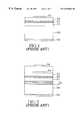
- FIG. 1illustrates the structure of a prior art surface-emitting type LED, wherein a lower cladding layer 21 is formed on the light-absorbing substrate 20 first, and then an active layer 22 is formed on the lower cladding layer 21 , and an upper cladding layer 23 is subsequently formed on the active layer 22 , so as to form a double heterostructure.
- the wavelength of the light emitted from such an LEDis dependent on the ratio of the composition of the active layer.
- each cladding layeris higher than that of the active layer, such that not only the carrier injection rate can be increased but also so that the light emitted from the active layer will not be absorbed by the cladding layers.
- a front metal electrode 24is coated on the light-emitting surface of the LED, and a rear electrode 25 is coated on the surface of the substrate 20 opposite to the surface on which the double heterostructure is formed. Since such a vertical type LED uses a light-absorbing substrate, for example, a GaAs substrate, which can absorb the light with wavelengths from 570 nm to 650 nm, its light-emitting efficiency will be reduced. Therefore, how to overcome the light absorption problem caused by the substrate is a key to improve the light-emitting efficiency of such an LED.
- an alternative conventional structureas illustrated in FIG. 2, has been provided by adding a current-block region 34 and a Bragg reflector layer 33 .
- the current-block region 34is formed on the upper cladding layer 23 and is of the same material as that of the upper cladding layer 23 but has different doping type.
- the current-block region 34can increase the current-spreading area, and thus improve the light-emnitting efficiency.
- the Bragg reflector layer 33which is formed between the light-absorbing substrate 20 and the lower cladding layer 21 can reflect the light directed to the light-absorbing substrate 20 and thus increase the light-emitting efficiency.
- the Bragg reflector layer 33is manufactured by iterately stacking a pair of two different layers with different refraction indexes. The range of the reflection angle of the Bragg reflector layer depends on the difference between the refraction indexes of the two layers of the pair.
- the material of the pairis restricted to be a compound semiconductor, the difference between the refraction indexes of the two layers of the pair is very limited, and thus merely the almost vertical incident light can be reflected by the Bragg reflector layer, while other incident light can pass the Bragg reflector layer and be absorbed by the substrate. Therefore, its effect of avoiding light from being absorbed by the substrate is very limited.
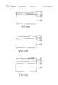
- FIG. 3Another conventional structure, as illustrated in FIG. 3, has been provided, wherein the heterostructure 36 of an LED is formed on a temporal light-absorbing substrate 20 to meet the requirement of lattice match, and after the formation of the heterostructure 36 is completed, the temporal substrate 20 is removed, and then a transparent conductive substrate 35 is attached to the heterostructure 36 by using the technique of thermal wafer bonding.
- the transparent conductive substrate 35will increase the current-spreading area and will not absorb the light emitted from the active layer, and thus will increase the light-emitting efficiency.
- the concept of the thermal wafer bonding technique which is used to combine the heterostructure 36 with the transparent conductive substrate 35is that the difference between the thermal expansion coefficients of two different materials will generate a single axis press, during a thermal process, which will force the generation of the binding, caused by atom-to-atom Van der Waals' force, between the heterostructure 36 and the transparent conductive substrate 35 .
- the thermal bonding machineshould be specially designed, but also, that the surfaces of the transparent conductive substrate 35 and the light emitting heterostructure 36 must be of the same lattice direction so as to obtain enough bonding force and low resistance on the bonding surfaces thereof. Therefore, such a conventional method is very complicated and very difficult in manufacturing, and thus its yield rate is hard to increase.
- a conventional gallium nitride-based light-emitting device using sapphire substratemust be manufactured as a lateral device, as illustrated in FIG. 4, for the reason that the sapphire substrate is insulated.
- Its structurecomprises a sapphire substrate 40 on which a buffer layer 41 , an n type lower cladding layer 42 , an active layer 43 , a p type upper cladding layer 44 and a p type ohmic contact layer 45 are formed serially as well as a front electrode 46 and a lateral rear electrode 47 which are formed subsequently.
- Silicon carbidehas also been used as a substrate for a conventional gallium nitride-based light-emitting device.
- silicon carbideis conductive and the light-emitting device using silicon carbide substrate can be made to have vertical electrodes, silicon carbide is hard to manufacture and the cost thereof is very high.
- Conventional light-emitting devices using insulated substratescannot be made to have traditional vertical type electrodes but must be of a lateral electrode structure. Therefore, not only special wiring mechanisms and special packaging techniques are needed, but also the area of a die is increased, so that the manufacturing process thereof will become very complicated and the cost for each unit is increased.
- adding a current-block regionneeds complicated MOCVD epitaxial processes, and the Bragg reflector layer can only reflect the light with an incident angle within a specific range;
- gallium nitride-based light-emitting devices using sapphire substratescannot be made to have vertical type electrodes, and thus increase the cost for each unit.
- An objective of the present inventionis to overcome the reduction of light-emitting efficiency by adapting a light-absorbing substrate.
- Another objective of the present inventionis to provide a method for easily combining a substrate with a light emitting semiconductor structure so as to reduce the complexity and difficulty of the manufacturing process and greatly increase the yield rate.
- a further objective of the present inventionis to simplify the manufacturing process of the current-block region and provide an effective current-spreading effect to improve light-emitting efficiency.
- a still further objective of the present inventionis to provide a manufacturing process which can easily convert the semiconductor light-emitting device with lateral electrode structure to be the one having a vertical type electrode structure so as to effectively reduce the area for an LED die and facilitate subsequent wiring and packaging processes using traditional mechanisms.
- a light-emnitting devicecomprises
- a semiconductor stack structurefor generating light in response to a conduction of current
- a reflection layerprovided on a main surface of the semiconductor stack structure for reflecting light generated from the stack structure and directed to the reflection layer
- the reflection layermay comprises at least one area with inferior conductivity functioned as a current-block region.
- a method for manufacturing a light-emitting devicecomprises the steps of:
- the light-absorbing substratehas been removed during the manufacturing process, and thus totally overcome the problem of reduction of light-emitting efficiency caused by using a light-absorbing substrate.
- the light-emitting devicehas a reflection layer which can effectively reflect the light directed to the substrate, and thus can improve the light-emitting efficiency of a surface-emitting type LED.
- the reflection layer of the present inventioncan comprise a single metal layer or multiple metal layers which can function as an intervention layer for facilitating the combination of the second substrate and the light emitting semiconductor structure. Therefore, not only the difficulties of conventional thermal wafer bonding can be avoided, but also the limitation to the choice of the material of the second substrate can be lessened.
- the current-block regioncan be formed during the process of forming the reflection layer, and thus greatly simplify the manufacturing process of the current-block region.
- the method of the present inventioncan be directly used to make a light-emitting device which originally utilized an insulated substrate to be one of having a vertical type electrode structure. Therefore, not only the wafer area used for a die can be effectively reduced, but also the final stage of the manufacturing can use the traditional wiring and packaging process. Further, it can provide a cleavage to divide the dies from each other, and thus it is suitable for making a laser diode.
- FIG. 1is a cross-sectional view illustrating the structure of a prior surface-emitting type light-emitting device
- FIG. 2is a cross-sectional view illustrating the structure of another prior surface-emitting type light-emitting device
- FIG. 3is a cross-sectional view illustrating the structure of a further prior surface-emitting type light-emitting device
- FIG. 4is a cross-sectional view illustrating the structure of a prior surface-emitting type light-emitting device manufactured by using an insulated substrate;
- FIG. 5is a cross-sectional view illustrating the structure of a surface-emitting type light-emitting device implemented according to the present invention
- FIGS. 6 a - 6 gare schematic views illustrating the manufacturing process of a surface-emitting type light-emitting device according to an embodiment of the present invention.
- FIGS. 7 a - 7 dare schematic views illustrating the manufacturing process of a surface-emitting type light-emitting device according to another embodiment of the present invention.
- FIGS. 8 a - 8 dare schematic views illustrating the manufacturing process of a surface-emitting type light-emitting device according to a further embodiment of the present invention.
- FIGS. 9 a - 9 eare schematic views illustrating the manufacturing process of a surface-emitting type light-emitting device using an insulated substrate according to an embodiment of the present invention.
- FIGS. 1O a - 10 care schematic views illustrating the manufacturing process of a surface-emitting type light-emitting device using an insulated substrate according to another embodiment of the present invention.
- a reflection layeris added between the light emitting heterostructure and the conductive substrate.
- a current-block regioncan be provided during the manufacturing process of the reflection layer. Therefore, it does not need to manufacture the current-block region by using two more MOCVD epitaxial processes, and thus reduce the complexity and cost of the manufacturing process.
- incident lightcan only penetrate the surface of the reflection layer and will be reflected by dipoles in the reflection layer, and metal can reflect the light with any incident angle. Therefore, the reflection layer can provide an effective reflection of light to prevent the light from being absorbed by the substrate.
- the reflection layercan be used as an intervention layer for the combination of the light emitting heterostructure and the substrate, and thus the process of the combination is much easier and simpler than that of thermal wafer bonding.
- the process of adding a reflection layer between the heterostructure of a light-emitting device using an insulated substrate and another substrate and then removing the insulated substratecan manufacture a gallium nitride-based light-emitting device having vertical type electrode structure which can facilitate the process of wiring and packaging of a die and can reduce the wafer area used for a die so as to reduce the cost.
- FIG. 5illustrates the structure of a surface-emitting type light-emitting device according to the present invention which comprises a metal reflection layer 8 , a ohmic contact layer 7 , an upper cladding layer 6 , an active layer 5 , a lower cladding layer 4 , a front electrode 11 and rear electrode 10 .
- n type AlGaInP lower cladding layer 121there are serially epitaxially formed an n type AlGaInP lower cladding layer 121 , a AlGahiP active layer 122 which is of a conventional structure and can be of a single-quantum-well structure (SQW) or a multiple-quantum-well structure (MQW), a p type AlGalnP upper cladding layer 123 and an ohmic contact layer 124 which consists of a p type InGaP layer and a p type GaAs layer.
- SQLsingle-quantum-well structure
- MQWmultiple-quantum-well structure
- part of the p type ohmic contact layer 124is removed by using an etching technique so as to expose the p type upper cladding layer 123 as illustrated in FIG. 6 b.
- a metal reflection layer 125is subsequently coated over the p type ohmic contact layer 124 and the p type upper cladding layer 123 by using a coating technique or sputtering technique as illustrated in FIG. 6 c.
- a p type conductive substrate 126 serving as a second substrateis thermally combined with the metal reflection layer 125 , and then the first n type GaAs substrate 120 is removed as illustrated in FIG. 6 d. Subsequently, a front metal electrode 128 and a rear metal electrode 127 are manufactured as illustrated in FIG. 6 e.
- Reflection layer 125can form effective ohmic contact with the p type ohmic contact layer 124 , but forms Schottky contact with the p type upper cladding layer 123 .
- the metal ohmic contacthas very good conductivity, and can not only function as a current-spreading path but also can effectively reflect the light emitted from the active layer 122 since the metal reflection layer 125 can reflect light with any incident angle.
- the Schottky contacthas poor conductivity, and functions as a current-block region. However, the Schottky contact area can also reflect the light emitted from the active layer 122 .
- FIG. 6 fshows the distribution of the input current in the light-emitting device of this embodiment.
- the metal reflection layer 125can effectively spread the current and thus improve the light-emitting efficiency.
- FIG. 6 gshows how the metal reflection layer 125 reflects the light emitted from the active layer 122 to prevent the light form being absorbed by the substrate 126 , so as to improve the light-emitting efficiency.
- n type GaAs substrate 130there are serially epitaxially formed an n type AIGaInP lower cladding layer 131 , a AlGaInP active layer 132 which is of a conventional structure and can be of a single-quantum-well structure (SQW) or a multiple-quantum-well structure (MQW), a p type AlGaInP upper cladding layer 133 and a p type ohmic contact layer 134 .
- SQLsingle-quantum-well structure
- MQWmultiple-quantum-well structure
- a metal reflection layer 135is subsequently coated over the p type ohmic contact layer 134 by using a coating technique or sputtering technique, and then part of the p type reflection layer 135 is removed by using an etching technique so as to expose the p type ohmic contact layer 134 as illustrated in FIG. 7 b.
- a p type conductive substrate 136 serving as a second substrateis thermally combined with the metal reflection layer 135 , and then the first n type GaAs substrate 130 is removed as illustrated in FIG. 7 c.
- a front metal electrode 138 and a rear metal electrode 137are manufactured as illustrated in FIG. 7 d.
- the metal reflection layer 135can form effective ohmic contact with the p type ohmic contact layer 134 .
- the function of the ohmic contactis the same as that described in Embodiment 1.
- the gap between the exposed p type ohmic contact layer 134 and the p type second substrate 136can function as a current-block region.
- the refraction index (n) of the AlGalnP upper cladding layer 133is about 3.5, while the refraction index of the gap between the exposed p type ohmic contact layer 134 and the p type second substrate 136 is about 1.
- the light emitted from the active layer 132 and directed to the gap between the exposed p type ohmic contact layer 134 and the p type second substrate 136will pass from a medium with a bigger refraction index to a medium with a smaller refraction index, and thus the gap can also reflect the light.
- the current distribution and the reflection of the light emitted from the active layer of this embodimentare the same as that of the Embodiment 1.
- n type AlGaInP lower cladding layer 141there are serially epitaxially formed an n type AlGaInP lower cladding layer 141 , a AlGaInP active layer 142 which is of a conventional structure and can be of a single-quantum-well structure (SQW) or a multiple-quantum-well structure (MQW), a p type AlGaInP upper cladding layer 143 and a p type ohmic contact layer 144 .
- SQLsingle-quantum-well structure
- MQWmultiple-quantum-well structure
- a metal reflection layer 145is coated on a p type second substrate 146 by using a coating technique or sputtering technique, and then part of the metal reflection layer 145 is removed so as to expose the p type second substrate 146 , as illustrated in FIG. 8 b. Subsequently, the metal reflection layer 145 is thermally combined with the ohmic contact layer 144 , and then the first n type GaAs substrate 140 is removed, as illustrated in FIG. 8 c. Finally, a front metal electrode 148 and a rear metal electrode 147 are manufactured as illustrated in FIG. 8 d.
- the metal reflection layer 145can form effective ohmic contact with the p type ohmic contact layer 144 .
- the function of the ohmic contact and the function of the gap between the exposed p type second substrate 146 and the ohmic contact layer 144are the same as that described in Embodiment 2.
- a coating pattern 200is formed on the p type ohmic contact layer 155 by a photo-lithographic process, as illustrated in FIG. 9 b.
- a metal reflection layer 156is coated on the coating pattern 200 which is on the p type ohmic contact layer 155 by using a coating technique or sputtering technique, as illustrated in FIG. 9 c.
- a p type second substrate 157is thermally combined with the metal reflection layer 156 , followed by removing the first sapphire substrate 150 , as illustrated in FIG. 9 d.
- a front metal electrode 159 and a rear metal electrode 158are manufactured, and thus a gallium nitride-based light-emitting device with vertical type electrode structure is manufactured, as illustrated in FIG. 9 e.
- the metal reflection layer 156can form effective ohmic contact with the p type ohmic contact layer 155 .
- the function of the ohmic contact and the function of the exposed gap between the p type second substrate 157 and the ohmic contact layer 155are the same as that described in Embodiment 2.
- n type GaN buffer layer 161on a first insulated sapphire substrate 160 , there are serially epitaxially formed an n type GaN buffer layer 161 , an n type AlGaN lower cladding layer 162 , an InGaN active layer 163 which is of a conventional structure and can be of a single-quantum-well structure or a multiple-quantum-well structure, a p type AlGaN upper cladding layer 164 and a p type GaN ohmic contact layer 165 .
- a metal reflection layer pattern 201is coated on a p type second substrate 166 , and then the metal reflection layer 201 is thermally combined with the ohmic contact layer 165 , as illustrated in FIG. 10 b.
- the first insulated sapphire substrate 160is removed, and then a front electrode 168 and a rear electrode 167 are manufactured, so as to manufacture a gallium nitride-based light-emitting device with vertical type electrode structure, as illustrated in FIG. 10 c.
- the metal reflection layer 201can form effective ohmic contact with the p type ohmic contact layer 165 .
- the function of the ohmic contact and the function of the gap between the exposed p type second substrate 166 and the ohmic contact layer 165are the same as that described in Embodiment 2.
- the reflection layercan be a single layer structure of titanium (Ti), aluminum (Al) or gold (Au) or a multiple layer structure of gold/germanium (Au/Ge), titanium/aluminum (Ti/Al) or nickel/gold (Ni/Au).
- the material of the second substrate of the embodimentscan be a compound semiconductor consisting of germanium (Ge) and silicon (Si), a compound semiconductor consisting of gallium phosphide (GaP) and indium phosphide (InP) or a conductive oxide such as indium-tin oxide (ITO) or zinc oxide (ZnO).
- the current-block regioncan made of an insulated oxide or an insulated nitride.
- the electrode structure of the present inventioncan be of a lateral type if in a different embodiment the lateral type electrode structure is required.
Landscapes
- Led Devices (AREA)
Abstract
Description
Claims (9)
Priority Applications (1)
| Application Number | Priority Date | Filing Date | Title |
|---|---|---|---|
| US09/434,316US6492661B1 (en) | 1999-11-04 | 1999-11-04 | Light emitting semiconductor device having reflection layer structure |
Applications Claiming Priority (1)
| Application Number | Priority Date | Filing Date | Title |
|---|---|---|---|
| US09/434,316US6492661B1 (en) | 1999-11-04 | 1999-11-04 | Light emitting semiconductor device having reflection layer structure |
Publications (1)
| Publication Number | Publication Date |
|---|---|
| US6492661B1true US6492661B1 (en) | 2002-12-10 |
Family
ID=23723734
Family Applications (1)
| Application Number | Title | Priority Date | Filing Date |
|---|---|---|---|
| US09/434,316Expired - LifetimeUS6492661B1 (en) | 1999-11-04 | 1999-11-04 | Light emitting semiconductor device having reflection layer structure |
Country Status (1)
| Country | Link |
|---|---|
| US (1) | US6492661B1 (en) |
Cited By (55)
| Publication number | Priority date | Publication date | Assignee | Title |
|---|---|---|---|---|
| US20020093023A1 (en)* | 1997-06-03 | 2002-07-18 | Camras Michael D. | III-Phosphide and III-Arsenide flip chip light-emitting devices |
| US20020170488A1 (en)* | 2001-05-18 | 2002-11-21 | Matsushita Electric Industrial Co., Ltd. | Method for manufacturing semiconductor substrate |
| US20040026703A1 (en)* | 2002-08-07 | 2004-02-12 | Shin-Etsu Handotai Co., Ltd. | Light emitting element and method for manufacturing the same |
| WO2003052838A3 (en)* | 2001-12-13 | 2004-05-27 | Rensselaer Polytech Inst | Light-emitting diode with planar omni-directional reflector |
| US20040211968A1 (en)* | 2003-04-24 | 2004-10-28 | Ming-Der Lin | Light-emitting diode and method for manufacturing the same |
| US20050045893A1 (en)* | 2003-08-28 | 2005-03-03 | Ludowise Michael J. | Resonant cavity light emitting device |
| US20050104078A1 (en)* | 2003-11-13 | 2005-05-19 | Ite Compound Semiconductor Corporation | Light-emitting diode having chemical compound based reflective structure |
| US20050173692A1 (en)* | 2002-12-27 | 2005-08-11 | Park Young H. | Vertical GaN light emitting diode and method for manufacturing the same |
| US20050173725A1 (en)* | 2004-02-06 | 2005-08-11 | Sanyo Electric Co., Ltd. | Nitride-based light-emitting device and method of manufacturing the same |
| US20050285126A1 (en)* | 2004-05-06 | 2005-12-29 | Yifeng Wu | LED fabrication via ion implant isolation |
| US20060027818A1 (en)* | 2001-07-17 | 2006-02-09 | Yoo Myung C | Diode having high brightness and method thereof |
| US20060054919A1 (en)* | 2004-08-27 | 2006-03-16 | Kyocera Corporation | Light-emitting element, method for manufacturing the same and lighting equipment using the same |
| KR100668306B1 (en) | 2004-10-20 | 2007-01-12 | 삼성전자주식회사 | Edge-emitting semiconductor laser diode and manufacturing method thereof |
| WO2007037762A1 (en)* | 2005-09-29 | 2007-04-05 | Tinggi Technologies Private Limited | Fabrication of semiconductor devices for light emission |
| DE102005061797A1 (en)* | 2005-12-23 | 2007-07-05 | Osram Opto Semiconductors Gmbh | Luminescence diode chip arrangement, has current barrier formed of semiconductor material of epitaxial layer sequence and of current expansion layer material |
| US20080061311A1 (en)* | 2005-01-24 | 2008-03-13 | Cree, Inc. | Led with current confinement structure and surface roughening |
| CN100388515C (en)* | 2005-09-30 | 2008-05-14 | 晶能光电(江西)有限公司 | Semiconductor light emitting device and manufacturing method thereof |
| US20080121908A1 (en)* | 2004-04-07 | 2008-05-29 | Shu Yuan | Fabrication of Reflective Layer on Semconductor Light Emitting Devices |
| US20080128722A1 (en)* | 2004-03-15 | 2008-06-05 | Shu Yuan | Fabrication of Semiconductor Devices |
| US20080164480A1 (en)* | 2003-09-19 | 2008-07-10 | Xuejun Kang | Fabrication of Semiconductor Devices |
| US20080210970A1 (en)* | 2003-09-19 | 2008-09-04 | Tinggi Technologies Private Limited | Fabrication of Conductive Metal Layer on Semiconductor Devices |
| US20080224173A1 (en)* | 2005-10-19 | 2008-09-18 | Tinggi Technologies Private Limited | Fabrication Transistors |
| CN100433379C (en)* | 2004-02-25 | 2008-11-12 | 三垦电气株式会社 | Light-emitting semiconductor device and method of fabrication |
| US20080303034A1 (en)* | 2007-06-08 | 2008-12-11 | Kuo-Chin Huang | Light-emitting gallium nitride-based III-V group compound semiconductor device and manufacturing method thereof |
| US20090104726A1 (en)* | 2003-11-12 | 2009-04-23 | Cree, Inc. | LED Fabrication Via Ion Implant Isolation |
| US20090166659A1 (en)* | 2004-09-22 | 2009-07-02 | Cree, Inc. | High Efficiency Group III Nitride LED with Lenticular Surface |
| US20090242929A1 (en)* | 2008-03-31 | 2009-10-01 | Chao-Kun Lin | Light emitting diodes with patterned current blocking metal contact |
| US7622746B1 (en) | 2006-03-17 | 2009-11-24 | Bridgelux, Inc. | Highly reflective mounting arrangement for LEDs |
| US20100006883A1 (en)* | 2001-07-23 | 2010-01-14 | Cree,Inc. | Light emitting diodes including barrier layers/sublayers and manufacturing methods therefor |
| US20100047996A1 (en)* | 2005-12-20 | 2010-02-25 | Tinggi Technologies Private Limited | Localized annealing during semiconductor device fabrication |
| US20100117107A1 (en)* | 2006-09-04 | 2010-05-13 | Shu Yuan | Electrical current distribution in light emitting devices |
| EP2190036A1 (en)* | 2008-11-24 | 2010-05-26 | LG Innotek Co., Ltd. | Light emitting device and method for manufacturing the same |
| US20100270573A1 (en)* | 2009-04-28 | 2010-10-28 | Sung Min Hwang | Light emitting device, light emitting device package, and lighting system including the same |
| US20100276715A1 (en)* | 2009-05-04 | 2010-11-04 | Sung Min Hwang | Light emitting device, light emitting device package and lighting system including the same |
| US20100295014A1 (en)* | 2006-08-16 | 2010-11-25 | Xuejun Kang | Improvements in external light efficiency of light emitting diodes |
| CN101937957A (en)* | 2010-08-11 | 2011-01-05 | 中国科学院半导体研究所 | Fabrication method of gallium nitride-based vertical structure light-emitting diode electrode structure |
| US20110001164A1 (en)* | 2005-07-25 | 2011-01-06 | Jin Sik Choi | Semiconductor light emitting device and fabrication method thereof |
| US20110008922A1 (en)* | 2004-06-30 | 2011-01-13 | David Todd Emerson | Methods of forming light emitting devices having current reducing structures |
| CN102347411A (en)* | 2010-07-23 | 2012-02-08 | Lg伊诺特有限公司 | Light emitting device, light emitting device package comprising same and lighting system |
| US8236585B2 (en) | 2001-10-22 | 2012-08-07 | Lg Electronics Inc. | Method of making diode having reflective layer |
| TWI381551B (en)* | 2008-08-01 | 2013-01-01 | Epistar Corp | Light-emitting element comprising composite plating substrate |
| US20130001617A1 (en)* | 2011-06-30 | 2013-01-03 | Ho Sang Kwack | Light emitting device |
| US8471269B2 (en) | 2004-07-27 | 2013-06-25 | Cree, Inc. | Light emitting devices having roughened/reflective contacts and methods of fabricating same |
| US20130207118A1 (en)* | 2010-11-03 | 2013-08-15 | Deyuan Xiao | Light emitting diode and fabrication method thereof |
| CN103325912A (en)* | 2012-03-19 | 2013-09-25 | 丰田合成株式会社 | Group III nitride semiconductor light-emitting element and method for producing the same |
| CN103489977A (en)* | 2013-09-29 | 2014-01-01 | 映瑞光电科技(上海)有限公司 | Light-emitting diode with all-dimensional reflecting mirror and corresponding method of light-emitting diode |
| US20140264430A1 (en)* | 2011-11-07 | 2014-09-18 | Koninklijke Philps N.V. | P-contact with more uniform injection and lower optical loss |
| EP2362444A3 (en)* | 2010-02-25 | 2015-03-11 | LG Innotek Co., Ltd. | Light emitting device, light emitting device package and lighting system |
| US9000468B2 (en) | 2001-10-26 | 2015-04-07 | Lg Innotek Co., Ltd. | Diode having vertical structure |
| CN104617191A (en)* | 2015-01-14 | 2015-05-13 | 映瑞光电科技(上海)有限公司 | LED vertical chip with current block structure and preparation method thereof |
| CN105609596A (en)* | 2015-09-11 | 2016-05-25 | 映瑞光电科技(上海)有限公司 | LED vertical chip possessing current blocking structure and manufacturing method thereof |
| US20160190396A1 (en)* | 2014-12-26 | 2016-06-30 | Lg Innotek Co., Ltd. | Light emitting device, light emitting device array and lighting apparatus including the same |
| US9905731B2 (en) | 2004-09-22 | 2018-02-27 | Cree, Inc. | High output group III nitride light emitting diodes |
| US20180097160A1 (en)* | 2015-04-15 | 2018-04-05 | Koninklijke Philips N.V. | Light emitting device with reflector and a top contact |
| CN112054102A (en)* | 2020-09-14 | 2020-12-08 | 东莞市中晶半导体科技有限公司 | LED chip, display module and display screen |
Citations (3)
| Publication number | Priority date | Publication date | Assignee | Title |
|---|---|---|---|---|
| US5502316A (en) | 1993-03-19 | 1996-03-26 | Hewlett-Packard Company | Wafer bonding of light emitting diode layers |
| US5563422A (en) | 1993-04-28 | 1996-10-08 | Nichia Chemical Industries, Ltd. | Gallium nitride-based III-V group compound semiconductor device and method of producing the same |
| US5744829A (en) | 1995-12-28 | 1998-04-28 | Showa Denko K. K. | A1GaInP light emitting diode |
- 1999
- 1999-11-04USUS09/434,316patent/US6492661B1/ennot_activeExpired - Lifetime
Patent Citations (3)
| Publication number | Priority date | Publication date | Assignee | Title |
|---|---|---|---|---|
| US5502316A (en) | 1993-03-19 | 1996-03-26 | Hewlett-Packard Company | Wafer bonding of light emitting diode layers |
| US5563422A (en) | 1993-04-28 | 1996-10-08 | Nichia Chemical Industries, Ltd. | Gallium nitride-based III-V group compound semiconductor device and method of producing the same |
| US5744829A (en) | 1995-12-28 | 1998-04-28 | Showa Denko K. K. | A1GaInP light emitting diode |
Cited By (148)
| Publication number | Priority date | Publication date | Assignee | Title |
|---|---|---|---|---|
| US20040227148A1 (en)* | 1997-06-03 | 2004-11-18 | Camras Michael D. | III-Phosphide and III-Arsenide flip chip light-emitting devices |
| US7268371B2 (en) | 1997-06-03 | 2007-09-11 | Philips Lumileds Lighting Company, Llc | Light extraction from a semiconductor light emitting device via chip shaping |
| US20060011935A1 (en)* | 1997-06-03 | 2006-01-19 | Krames Michael R | Light extraction from a semiconductor light emitting device via chip shaping |
| US6946309B2 (en) | 1997-06-03 | 2005-09-20 | Lumileds Lighting U.S., Llc | III-Phosphide and III-Arsenide flip chip light-emitting devices |
| US6784463B2 (en) | 1997-06-03 | 2004-08-31 | Lumileds Lighting U.S., Llc | III-Phospide and III-Arsenide flip chip light-emitting devices |
| US20020093023A1 (en)* | 1997-06-03 | 2002-07-18 | Camras Michael D. | III-Phosphide and III-Arsenide flip chip light-emitting devices |
| US20020170488A1 (en)* | 2001-05-18 | 2002-11-21 | Matsushita Electric Industrial Co., Ltd. | Method for manufacturing semiconductor substrate |
| US7306675B2 (en)* | 2001-05-18 | 2007-12-11 | Matsushita Electric Industrial Co., Ltd. | Method for manufacturing semiconductor substrate |
| US9136424B2 (en) | 2001-07-17 | 2015-09-15 | Lg Innotek Co., Ltd. | Diode having high brightness and method thereof |
| US7582912B2 (en)* | 2001-07-17 | 2009-09-01 | Lg Electronics Inc. | Diode having high brightness and method thereof |
| US10147841B2 (en) | 2001-07-17 | 2018-12-04 | Lg Innotek Co., Ltd. | Diode having high brightness and method thereof |
| US7939849B2 (en) | 2001-07-17 | 2011-05-10 | Lg Electronics Inc. | Diode having high brightness and method thereof |
| US8674386B2 (en) | 2001-07-17 | 2014-03-18 | Lg Innotek Co. Ltd. | Diode having high brightness and method thereof |
| US9640713B2 (en) | 2001-07-17 | 2017-05-02 | Lg Innotek Co., Ltd. | Diode having high brightness and method thereof |
| US20060027818A1 (en)* | 2001-07-17 | 2006-02-09 | Yoo Myung C | Diode having high brightness and method thereof |
| US10553744B2 (en) | 2001-07-17 | 2020-02-04 | Lg Innotek Co., Ltd. | Diode having high brightness and method thereof |
| US8907366B2 (en) | 2001-07-23 | 2014-12-09 | Cree, Inc. | Light emitting diodes including current spreading layer and barrier sublayers |
| US8269241B2 (en) | 2001-07-23 | 2012-09-18 | Cree, Inc. | Light emitting diodes including barrier layers/sublayers and manufacturing methods therefor |
| US8604502B2 (en) | 2001-07-23 | 2013-12-10 | Cree, Inc. | Light emitting diodes including barrier sublayers |
| US20100006883A1 (en)* | 2001-07-23 | 2010-01-14 | Cree,Inc. | Light emitting diodes including barrier layers/sublayers and manufacturing methods therefor |
| US8759129B2 (en) | 2001-10-22 | 2014-06-24 | Lg Innotek Co., Ltd | Method of making diode having reflective layer |
| US9406837B2 (en) | 2001-10-22 | 2016-08-02 | Lg Innotek Co., Ltd | Method of making diode having reflective layer |
| US8236585B2 (en) | 2001-10-22 | 2012-08-07 | Lg Electronics Inc. | Method of making diode having reflective layer |
| US10326055B2 (en) | 2001-10-26 | 2019-06-18 | Lg Innotek Co., Ltd. | Diode having vertical structure |
| US9620677B2 (en) | 2001-10-26 | 2017-04-11 | Lg Innotek Co., Ltd. | Diode having vertical structure |
| US9000468B2 (en) | 2001-10-26 | 2015-04-07 | Lg Innotek Co., Ltd. | Diode having vertical structure |
| US10032959B2 (en) | 2001-10-26 | 2018-07-24 | Lg Innotek Co., Ltd. | Diode having vertical structure |
| WO2003052838A3 (en)* | 2001-12-13 | 2004-05-27 | Rensselaer Polytech Inst | Light-emitting diode with planar omni-directional reflector |
| US6784462B2 (en) | 2001-12-13 | 2004-08-31 | Rensselaer Polytechnic Institute | Light-emitting diode with planar omni-directional reflector |
| US20040026703A1 (en)* | 2002-08-07 | 2004-02-12 | Shin-Etsu Handotai Co., Ltd. | Light emitting element and method for manufacturing the same |
| US6759689B2 (en)* | 2002-08-07 | 2004-07-06 | Shin-Etsu Handotai Co., Ltd. | Light emitting element and method for manufacturing the same |
| US20050173692A1 (en)* | 2002-12-27 | 2005-08-11 | Park Young H. | Vertical GaN light emitting diode and method for manufacturing the same |
| US7268372B2 (en)* | 2002-12-27 | 2007-09-11 | Samsung Electro-Mechanics Co., Ltd. | Vertical GaN light emitting diode and method for manufacturing the same |
| US20040211968A1 (en)* | 2003-04-24 | 2004-10-28 | Ming-Der Lin | Light-emitting diode and method for manufacturing the same |
| US6903381B2 (en)* | 2003-04-24 | 2005-06-07 | Opto Tech Corporation | Light-emitting diode with cavity containing a filler |
| US20050045893A1 (en)* | 2003-08-28 | 2005-03-03 | Ludowise Michael J. | Resonant cavity light emitting device |
| US7019330B2 (en) | 2003-08-28 | 2006-03-28 | Lumileds Lighting U.S., Llc | Resonant cavity light emitting device |
| US8034643B2 (en)* | 2003-09-19 | 2011-10-11 | Tinggi Technologies Private Limited | Method for fabrication of a semiconductor device |
| US20080210970A1 (en)* | 2003-09-19 | 2008-09-04 | Tinggi Technologies Private Limited | Fabrication of Conductive Metal Layer on Semiconductor Devices |
| US20080164480A1 (en)* | 2003-09-19 | 2008-07-10 | Xuejun Kang | Fabrication of Semiconductor Devices |
| US20090104726A1 (en)* | 2003-11-12 | 2009-04-23 | Cree, Inc. | LED Fabrication Via Ion Implant Isolation |
| US7943406B2 (en) | 2003-11-12 | 2011-05-17 | Cree, Inc. | LED fabrication via ion implant isolation |
| US20050104078A1 (en)* | 2003-11-13 | 2005-05-19 | Ite Compound Semiconductor Corporation | Light-emitting diode having chemical compound based reflective structure |
| US20050173725A1 (en)* | 2004-02-06 | 2005-08-11 | Sanyo Electric Co., Ltd. | Nitride-based light-emitting device and method of manufacturing the same |
| US7892874B2 (en) | 2004-02-06 | 2011-02-22 | Sanyo Electric Co., Ltd. | Nitride-based light-emitting device and method of manufacturing the same |
| CN100524852C (en)* | 2004-02-06 | 2009-08-05 | 三洋电机株式会社 | Nitride-based light emitting device and method for manufacturing the same |
| US20080064130A1 (en)* | 2004-02-06 | 2008-03-13 | Sanyo Electric Co., Ltd. | Nitride-based light-emitting device and method of manufacturing the same |
| US20090263925A1 (en)* | 2004-02-06 | 2009-10-22 | Sanyo Electric Co., Ltd | Nitride-based light-emitting device and method of manufacturing the same |
| US7592630B2 (en) | 2004-02-06 | 2009-09-22 | Sanyo Electric Co., Ltd. | Nitride-based light-emitting device and method of manufacturing the same |
| US7488613B2 (en) | 2004-02-06 | 2009-02-10 | Sanyo Electric Co., Ltd. | Nitride-based light-emitting device and method of manufacturing the same |
| CN100433379C (en)* | 2004-02-25 | 2008-11-12 | 三垦电气株式会社 | Light-emitting semiconductor device and method of fabrication |
| US20080128722A1 (en)* | 2004-03-15 | 2008-06-05 | Shu Yuan | Fabrication of Semiconductor Devices |
| US7763477B2 (en) | 2004-03-15 | 2010-07-27 | Tinggi Technologies Pte Limited | Fabrication of semiconductor devices |
| US8309377B2 (en) | 2004-04-07 | 2012-11-13 | Tinggi Technologies Private Limited | Fabrication of reflective layer on semiconductor light emitting devices |
| US20080121908A1 (en)* | 2004-04-07 | 2008-05-29 | Shu Yuan | Fabrication of Reflective Layer on Semconductor Light Emitting Devices |
| US20090309124A1 (en)* | 2004-05-06 | 2009-12-17 | Cree, Inc. | LED Fabrication via Ion Implant Isolation |
| US7943954B2 (en) | 2004-05-06 | 2011-05-17 | Cree, Inc. | LED fabrication via ion implant isolation |
| US7592634B2 (en)* | 2004-05-06 | 2009-09-22 | Cree, Inc. | LED fabrication via ion implant isolation |
| US20050285126A1 (en)* | 2004-05-06 | 2005-12-29 | Yifeng Wu | LED fabrication via ion implant isolation |
| US8704240B2 (en)* | 2004-06-30 | 2014-04-22 | Cree, Inc. | Light emitting devices having current reducing structures |
| US8163577B2 (en) | 2004-06-30 | 2012-04-24 | Cree, Inc. | Methods of forming light emitting devices having current reducing structures |
| US8436368B2 (en) | 2004-06-30 | 2013-05-07 | Cree, Inc. | Methods of forming light emitting devices having current reducing structures |
| US20110008922A1 (en)* | 2004-06-30 | 2011-01-13 | David Todd Emerson | Methods of forming light emitting devices having current reducing structures |
| US8669563B2 (en) | 2004-07-27 | 2014-03-11 | Cree, Inc. | Light emitting devices having roughened/reflective contacts and methods of fabricating same |
| US8471269B2 (en) | 2004-07-27 | 2013-06-25 | Cree, Inc. | Light emitting devices having roughened/reflective contacts and methods of fabricating same |
| US20060054919A1 (en)* | 2004-08-27 | 2006-03-16 | Kyocera Corporation | Light-emitting element, method for manufacturing the same and lighting equipment using the same |
| US8878209B2 (en) | 2004-09-22 | 2014-11-04 | Cree, Inc. | High efficiency group III nitride LED with lenticular surface |
| US20090242918A1 (en)* | 2004-09-22 | 2009-10-01 | Cree, Inc. | High Efficiency Group III Nitride LED with Lenticular Surface |
| US20090166659A1 (en)* | 2004-09-22 | 2009-07-02 | Cree, Inc. | High Efficiency Group III Nitride LED with Lenticular Surface |
| EP2270878B1 (en)* | 2004-09-22 | 2017-03-08 | Cree, Inc. | LED with a lenticular surface |
| US9905731B2 (en) | 2004-09-22 | 2018-02-27 | Cree, Inc. | High output group III nitride light emitting diodes |
| US8692267B2 (en) | 2004-09-22 | 2014-04-08 | Cree, Inc. | High efficiency Group III nitride LED with lenticular surface |
| US8183588B2 (en) | 2004-09-22 | 2012-05-22 | Cree, Inc. | High efficiency group III nitride LED with lenticular surface |
| US8174037B2 (en) | 2004-09-22 | 2012-05-08 | Cree, Inc. | High efficiency group III nitride LED with lenticular surface |
| US8154039B2 (en) | 2004-09-22 | 2012-04-10 | Cree, Inc. | High efficiency group III nitride LED with lenticular surface |
| KR100668306B1 (en) | 2004-10-20 | 2007-01-12 | 삼성전자주식회사 | Edge-emitting semiconductor laser diode and manufacturing method thereof |
| US8772792B2 (en) | 2005-01-24 | 2014-07-08 | Cree, Inc. | LED with surface roughening |
| US20080061311A1 (en)* | 2005-01-24 | 2008-03-13 | Cree, Inc. | Led with current confinement structure and surface roughening |
| US20100032704A1 (en)* | 2005-01-24 | 2010-02-11 | Cree, Inc. | Led with current confinement structure and surface roughening |
| US8541788B2 (en)* | 2005-01-24 | 2013-09-24 | Cree, Inc. | LED with current confinement structure and surface roughening |
| US8410490B2 (en) | 2005-01-24 | 2013-04-02 | Cree, Inc. | LED with current confinement structure and surface roughening |
| US8410499B2 (en) | 2005-01-24 | 2013-04-02 | Cree, Inc. | LED with a current confinement structure aligned with a contact |
| US20090121246A1 (en)* | 2005-01-24 | 2009-05-14 | Cree, Inc. | LED with current confinement structure and surface roughening |
| US20110001164A1 (en)* | 2005-07-25 | 2011-01-06 | Jin Sik Choi | Semiconductor light emitting device and fabrication method thereof |
| CN102569560A (en)* | 2005-07-25 | 2012-07-11 | Lg伊诺特有限公司 | Semiconductor light emitting device and fabrication method thereof |
| US9147797B2 (en) | 2005-07-25 | 2015-09-29 | Lg Innotek Co., Ltd. | Semiconductor light emitting device and fabrication method thereof |
| WO2007037762A1 (en)* | 2005-09-29 | 2007-04-05 | Tinggi Technologies Private Limited | Fabrication of semiconductor devices for light emission |
| US8004001B2 (en) | 2005-09-29 | 2011-08-23 | Tinggi Technologies Private Limited | Fabrication of semiconductor devices for light emission |
| US20080210969A1 (en)* | 2005-09-29 | 2008-09-04 | Tinggi Technologies Private Limited | Fabrication of Semiconductor Devices for Light Emission |
| CN100388515C (en)* | 2005-09-30 | 2008-05-14 | 晶能光电(江西)有限公司 | Semiconductor light emitting device and manufacturing method thereof |
| US20080224173A1 (en)* | 2005-10-19 | 2008-09-18 | Tinggi Technologies Private Limited | Fabrication Transistors |
| US8067269B2 (en) | 2005-10-19 | 2011-11-29 | Tinggi Technologies Private Limted | Method for fabricating at least one transistor |
| US20100047996A1 (en)* | 2005-12-20 | 2010-02-25 | Tinggi Technologies Private Limited | Localized annealing during semiconductor device fabrication |
| US8329556B2 (en) | 2005-12-20 | 2012-12-11 | Tinggi Technologies Private Limited | Localized annealing during semiconductor device fabrication |
| US20090127580A1 (en)* | 2005-12-23 | 2009-05-21 | Osram Opto Semiconductors Gmbh | Luminescence diode chip with current spreading layer and method for producing the same |
| US8017953B2 (en) | 2005-12-23 | 2011-09-13 | Osram Opto Semiconductors Gmbh | Luminescence diode chip with current spreading layer and method for producing the same |
| DE102005061797A1 (en)* | 2005-12-23 | 2007-07-05 | Osram Opto Semiconductors Gmbh | Luminescence diode chip arrangement, has current barrier formed of semiconductor material of epitaxial layer sequence and of current expansion layer material |
| DE102005061797B4 (en)* | 2005-12-23 | 2020-07-09 | Osram Opto Semiconductors Gmbh | Luminescence diode chip with current spreading layer and method for its production |
| US7622746B1 (en) | 2006-03-17 | 2009-11-24 | Bridgelux, Inc. | Highly reflective mounting arrangement for LEDs |
| US8324652B1 (en) | 2006-03-17 | 2012-12-04 | Bridgelux, Inc. | Highly reflective mounting arrangement for LEDs |
| US20100295014A1 (en)* | 2006-08-16 | 2010-11-25 | Xuejun Kang | Improvements in external light efficiency of light emitting diodes |
| US8395167B2 (en)* | 2006-08-16 | 2013-03-12 | Tinggi Technologies Private Limited | External light efficiency of light emitting diodes |
| US20100117107A1 (en)* | 2006-09-04 | 2010-05-13 | Shu Yuan | Electrical current distribution in light emitting devices |
| US8124994B2 (en) | 2006-09-04 | 2012-02-28 | Tinggi Technologies Private Limited | Electrical current distribution in light emitting devices |
| US20090275156A1 (en)* | 2007-06-08 | 2009-11-05 | Kuo-Chin Huang | Light-emitting gallium nitride-based III-V group compound semiconductor device and manufacturing method thereof |
| US8263991B2 (en)* | 2007-06-08 | 2012-09-11 | Formosa Epitaxy Incorporation | Light-emitting gallium nitride-based III-V group compound semiconductor device and manufacturing method thereof |
| US20080303034A1 (en)* | 2007-06-08 | 2008-12-11 | Kuo-Chin Huang | Light-emitting gallium nitride-based III-V group compound semiconductor device and manufacturing method thereof |
| US20090242929A1 (en)* | 2008-03-31 | 2009-10-01 | Chao-Kun Lin | Light emitting diodes with patterned current blocking metal contact |
| TWI381551B (en)* | 2008-08-01 | 2013-01-01 | Epistar Corp | Light-emitting element comprising composite plating substrate |
| EP2190036A1 (en)* | 2008-11-24 | 2010-05-26 | LG Innotek Co., Ltd. | Light emitting device and method for manufacturing the same |
| CN101740695B (en)* | 2008-11-24 | 2014-06-11 | Lg伊诺特有限公司 | Light emitting device and method for manufacturing the same |
| US8569784B2 (en) | 2008-11-24 | 2013-10-29 | Lg Innotek Co., Ltd. | Light emitting device and method for manufacturing the same |
| US8288786B2 (en) | 2008-11-24 | 2012-10-16 | Lg Innotek Co., Ltd. | Light emitting device and method for manufacturing the same |
| US8222660B2 (en)* | 2009-04-28 | 2012-07-17 | Lg Innotek Co., Ltd. | Light emitting device, light emitting device package, and lighting system including the same |
| US20100270573A1 (en)* | 2009-04-28 | 2010-10-28 | Sung Min Hwang | Light emitting device, light emitting device package, and lighting system including the same |
| US8373190B2 (en) | 2009-04-28 | 2013-02-12 | Lg Innotek Co., Ltd. | Light emitting device, light emitting device package, and lighting system including the same |
| US8513681B2 (en) | 2009-05-04 | 2013-08-20 | Lg Innotek Co., Ltd. | Light emitting device, light emitting device package and lighting system including the same |
| US8907363B2 (en) | 2009-05-04 | 2014-12-09 | Lg Innotek Co., Ltd. | Light emitting device, light emitting device package and lighting system including the same |
| CN101882658B (en)* | 2009-05-04 | 2014-11-19 | Lg伊诺特有限公司 | Light emitting device, light emitting device package and lighting system including the package |
| US20100276715A1 (en)* | 2009-05-04 | 2010-11-04 | Sung Min Hwang | Light emitting device, light emitting device package and lighting system including the same |
| CN101882658A (en)* | 2009-05-04 | 2010-11-10 | Lg伊诺特有限公司 | Light emitting device, light emitting device package and lighting system including the package |
| US9343640B2 (en) | 2009-05-04 | 2016-05-17 | Lg Innotek Co., Ltd. | Light emitting device, light emitting device package and lighting system including the same |
| EP2249405A3 (en)* | 2009-05-04 | 2014-01-08 | LG Innotek Co., Ltd. | Light emitting device, light emitting device package and lighting system including the same |
| US8222661B2 (en)* | 2009-05-04 | 2012-07-17 | Lg Innotek Co., Ltd. | Light emitting device, light emitting device package and lighting system including the same |
| EP2362444A3 (en)* | 2010-02-25 | 2015-03-11 | LG Innotek Co., Ltd. | Light emitting device, light emitting device package and lighting system |
| US9356195B2 (en)* | 2010-07-23 | 2016-05-31 | Lg Innotek Co., Ltd. | Light emitting device, light emitting device package comprising the same and lighting system |
| US10141478B2 (en) | 2010-07-23 | 2018-11-27 | Lg Innotek Co., Ltd. | Structure of a reflective electrode and an OHMIC layer of a light emitting device |
| US20150048308A1 (en)* | 2010-07-23 | 2015-02-19 | Lg Innotek Co., Ltd. | Light emitting device, light emitting device package comprising the same and lighting system |
| CN102347411A (en)* | 2010-07-23 | 2012-02-08 | Lg伊诺特有限公司 | Light emitting device, light emitting device package comprising same and lighting system |
| US8872212B2 (en) | 2010-07-23 | 2014-10-28 | Lg Innotek Co., Ltd. | Light emitting device, light emitting device package comprising the same and lighting system |
| CN101937957A (en)* | 2010-08-11 | 2011-01-05 | 中国科学院半导体研究所 | Fabrication method of gallium nitride-based vertical structure light-emitting diode electrode structure |
| US20130207118A1 (en)* | 2010-11-03 | 2013-08-15 | Deyuan Xiao | Light emitting diode and fabrication method thereof |
| US20130001617A1 (en)* | 2011-06-30 | 2013-01-03 | Ho Sang Kwack | Light emitting device |
| US9444016B2 (en)* | 2011-06-30 | 2016-09-13 | Lg Innotek Co., Ltd. | Light emitting device |
| US9312437B2 (en)* | 2011-11-07 | 2016-04-12 | Koninklijke Philips N.V. | P-contact with more uniform injection and lower optical loss |
| US9583679B2 (en) | 2011-11-07 | 2017-02-28 | Koninklijke Philips N.V. | P-contact with more uniform injection and lower optical loss |
| US20140264430A1 (en)* | 2011-11-07 | 2014-09-18 | Koninklijke Philps N.V. | P-contact with more uniform injection and lower optical loss |
| CN103325912A (en)* | 2012-03-19 | 2013-09-25 | 丰田合成株式会社 | Group III nitride semiconductor light-emitting element and method for producing the same |
| CN103325912B (en)* | 2012-03-19 | 2016-08-03 | 丰田合成株式会社 | Group iii nitride semiconductor light-emitting device and manufacture method thereof |
| CN103489977A (en)* | 2013-09-29 | 2014-01-01 | 映瑞光电科技(上海)有限公司 | Light-emitting diode with all-dimensional reflecting mirror and corresponding method of light-emitting diode |
| US9620683B2 (en)* | 2014-12-26 | 2017-04-11 | Lg Innotek Co., Ltd. | Light emitting device, light emitting device array and lighting apparatus including the same |
| JP2016127289A (en)* | 2014-12-26 | 2016-07-11 | エルジー イノテック カンパニー リミテッド | LIGHT EMITTING ELEMENT, LIGHT EMITTING ELEMENT ARRAY, AND LIGHTING DEVICE INCLUDING THE SAME |
| US20160190396A1 (en)* | 2014-12-26 | 2016-06-30 | Lg Innotek Co., Ltd. | Light emitting device, light emitting device array and lighting apparatus including the same |
| CN104617191A (en)* | 2015-01-14 | 2015-05-13 | 映瑞光电科技(上海)有限公司 | LED vertical chip with current block structure and preparation method thereof |
| US20180097160A1 (en)* | 2015-04-15 | 2018-04-05 | Koninklijke Philips N.V. | Light emitting device with reflector and a top contact |
| US10026881B2 (en)* | 2015-04-15 | 2018-07-17 | Koninklijke Philips N.V. | Light emitting device with reflector and a top contact |
| CN105609596A (en)* | 2015-09-11 | 2016-05-25 | 映瑞光电科技(上海)有限公司 | LED vertical chip possessing current blocking structure and manufacturing method thereof |
| CN112054102A (en)* | 2020-09-14 | 2020-12-08 | 东莞市中晶半导体科技有限公司 | LED chip, display module and display screen |
Similar Documents
| Publication | Publication Date | Title |
|---|---|---|
| US6492661B1 (en) | Light emitting semiconductor device having reflection layer structure | |
| KR102794687B1 (en) | Light-emitting device | |
| US7274040B2 (en) | Contact and omnidirectional reflective mirror for flip chipped light emitting devices | |
| US7319247B2 (en) | Light emitting-diode chip and a method for producing same | |
| US6825502B2 (en) | Light emitting element, method of manufacturing the same, and semiconductor device having light emitting element | |
| JP4091261B2 (en) | Semiconductor light emitting device and manufacturing method thereof | |
| JP4907842B2 (en) | Light emitting diode with planar omnidirectional reflector | |
| US8835938B2 (en) | Nitride semiconductor light-emitting element and method of manufacturing the same | |
| CN100386899C (en) | High-efficiency high-brightness total reflection light-emitting diode and its manufacturing method | |
| US20050035354A1 (en) | Light emiting diodes with current spreading layer | |
| JP2001144321A (en) | Light-emitting device and manufacturing method therefor | |
| CN105009308B (en) | Method and apparatus for creating porous reflective contact part | |
| US7554124B2 (en) | Nitride-based compound semiconductor light emitting device, structural unit thereof, and fabricating method thereof | |
| CN1198339C (en) | Structure of light emitting diode and its manufacturing method | |
| US10461223B2 (en) | Semiconductor device | |
| CN113707782B (en) | Flip-chip light emitting diode and preparation method thereof | |
| KR20180082194A (en) | Semiconductor light emitting device and method of manufacturing the same | |
| CN100334745C (en) | Light emitting semiconductor device and manufacturing method thereof | |
| US6169298B1 (en) | Semiconductor light emitting device with conductive window layer | |
| US20230078065A1 (en) | Forming method of flip-chip light emitting diode structure | |
| TW480740B (en) | Light-emitting semiconductor device with reflective layer structure and method for making the same | |
| US20240113262A1 (en) | Light-emitting device, backlight unit and display apparatus having the same | |
| KR20040013394A (en) | A Light Emitting Diode and A Method for Manufacturing thereof | |
| TW202343833A (en) | Light-emitting element | |
| CN118943266A (en) | Light emitting diode and light emitting device |
Legal Events
| Date | Code | Title | Description |
|---|---|---|---|
| AS | Assignment | Owner name:UNI LIGHT TECHNOLOGY INCORPORATION, TAIWAN Free format text:ASSIGNMENT OF ASSIGNORS INTEREST;ASSIGNOR:LAI, MU-JEN;REEL/FRAME:013275/0940 Effective date:20020710 Owner name:UNI LIGHT TECHNOLOGY INCORPORATION, TAIWAN Free format text:ASSIGNMENT OF ASSIGNORS INTEREST;ASSIGNOR:LAI, MU-JEN;REEL/FRAME:013345/0526 Effective date:20020710 | |
| STCF | Information on status: patent grant | Free format text:PATENTED CASE | |
| FEPP | Fee payment procedure | Free format text:PAT HOLDER CLAIMS SMALL ENTITY STATUS, ENTITY STATUS SET TO SMALL (ORIGINAL EVENT CODE: LTOS); ENTITY STATUS OF PATENT OWNER: SMALL ENTITY | |
| FEPP | Fee payment procedure | Free format text:PAT HOLDER NO LONGER CLAIMS SMALL ENTITY STATUS, ENTITY STATUS SET TO UNDISCOUNTED (ORIGINAL EVENT CODE: STOL); ENTITY STATUS OF PATENT OWNER: SMALL ENTITY Free format text:PAT HOLDER CLAIMS SMALL ENTITY STATUS, ENTITY STATUS SET TO SMALL (ORIGINAL EVENT CODE: LTOS); ENTITY STATUS OF PATENT OWNER: SMALL ENTITY | |
| FPAY | Fee payment | Year of fee payment:4 | |
| AS | Assignment | Owner name:UNI LIGHT TECHNOLOGY INCORPORATION, TAIWAN Free format text:EVIDENCE OF ASSIGNMENT;ASSIGNORS:CHIEN, FEN-REN;HONG, SCHANG-FING;REEL/FRAME:018731/0302 Effective date:20060811 | |
| FPAY | Fee payment | Year of fee payment:8 | |
| FPAY | Fee payment | Year of fee payment:12 |