US6489798B1 - Method and apparatus for testing image sensing circuit arrays - Google Patents
Method and apparatus for testing image sensing circuit arraysDownload PDFInfo
- Publication number
- US6489798B1 US6489798B1US09/538,905US53890500AUS6489798B1US 6489798 B1US6489798 B1US 6489798B1US 53890500 AUS53890500 AUS 53890500AUS 6489798 B1US6489798 B1US 6489798B1
- Authority
- US
- United States
- Prior art keywords
- voltage
- reset
- circuits
- rows
- columns
- Prior art date
- Legal status (The legal status is an assumption and is not a legal conclusion. Google has not performed a legal analysis and makes no representation as to the accuracy of the status listed.)
- Expired - Lifetime
Links
Images


Classifications
- H—ELECTRICITY
- H04—ELECTRIC COMMUNICATION TECHNIQUE
- H04N—PICTORIAL COMMUNICATION, e.g. TELEVISION
- H04N25/00—Circuitry of solid-state image sensors [SSIS]; Control thereof
- H04N25/70—SSIS architectures; Circuits associated therewith
- H04N25/76—Addressed sensors, e.g. MOS or CMOS sensors
- H—ELECTRICITY
- H04—ELECTRIC COMMUNICATION TECHNIQUE
- H04N—PICTORIAL COMMUNICATION, e.g. TELEVISION
- H04N17/00—Diagnosis, testing or measuring for television systems or their details
- H04N17/002—Diagnosis, testing or measuring for television systems or their details for television cameras
Definitions
- the inventionrelates generally to image sensing circuits arrays, and more particularly to the method and apparatus for testing the arrays.
- a conventional sensing arrayis composed of individual light sensitive circuits called pixels that are organized in rows and columns.
- a row of pixelshas a common line connecting the control gates of their respective access transistors. Data is passed from a pixel through its access transistor to a data line.
- Each column of pixelsis connected to a common data line.
- CMOS image sensor arrayscan employ several types of pixels.
- Passive pixel sensor circuitsare comprised of a simple photodiode and an access transistor.
- Active pixel sensor (APS) circuitshave added features including a reset transistor and a source follower amplifier.
- Individual sensor circuitsmay suffer from similar problems as the row lines and data lines, in that they may be either short circuited or open circuited and therefore do not perform their proper function. In order to overcome these problems, defects in the sensor array must be detected in order to select arrays that are acceptable for use.
- CMOS image sensorshave traditionally been relatively expensive devices, many of which used a technology known as charge coupled device (CCD). The nature of these devices did not permit the use of extensive integrated test features, therefore testing was primarily dependent on the use of external light sources. This traditional test method continued for the testing of CMOS image sensors such as those using APS circuits. Therefore, testing of integrated imager active pixel sensor arrays has required the use of expensive, calibrated light sources to perform optical testing of the sensors. Typically, during production testing, an image sensor would be exposed to light of varying intensity ranging from black to white. Measurements would be taken to determine the response of the array. The length of time required to perform these optical tests can be excessive, adding dramatically to the cost of the device. Reduction of test times and therefore costs can be accomplished by reducing the dependency of these tests on a calibrated light source.
- CCDcharge coupled device
- the accuracy of the testis also a concern. If two neighboring pixels were shorted together during the manufacturing process, the measured output would be the same as if the pixels were not shorted together. This occurs because both pixels have been exposed to the same intensity of light. The defect may go undetected until the device is placed in a system and tested under “real world” conditions. Unfortunately, detection of the defect is dependent on human viewing of the output as displayed on the viewing device (e.g. a cathode ray tube or liquid crystal display panel). As the number of pixels on an integrated circuit expands, it becomes increasingly difficult for a human to detect such faults.
- test circuitryintegrated on the same die as the sensor array for testing a specific pixel and transfer circuit arrangement.
- This arrangementinvolves a circuit for injecting a certain amount of charge into the transfer circuit and a smaller amount of charge to bias the photodiode. The difference between these two charges is indicative of the linear response of the pixel.
- the test circuitplaces a known amount of bias charge into the pixel. The pixel is not illuminated during testing, so this bias charge should be shifted out through the transfer circuit. This allows testing for the presence of the correct bias charge and for the proper photodiode response linearity.
- this systemdoes not account for the identification of problems with the row lines or data lines such as short circuits between adjacent lines or open circuits in an individual line.
- U.S. Pat. No.5,654,537which issued to Prater on Aug. 5, 1997 also proposes a system for testing an image scanner array having pixel sensor circuits arranged in rows and columns.
- Prater's apparatusincludes a reset voltage source having selectable voltage that may vary in amplitude between ground and the supply voltage levels.
- the photo-sensitive devices in the pixel sensor circuitsare cyclically tested using a different selected voltage for each cycle to reset the photosensitive devices in the pixel sensor circuits.
- the outputs of the pixel sensor circuitsare sensed to determine whether they are functioning properly.
- the reset voltage between ground and the power supplyas disclosed by Prater, the pixel sensor circuits are tested as if they had received different illumination levels without the need for a calibrated light source.
- the systemdoes not differentiate between adjacent pixel sensor circuits. Prater discloses supplying the variable reset voltage to the drain of the reset transistors in the pixel sensor circuits in the rows and columns. If two neighbouring pixels were shorted together, the measured output would be the same as if the pixels were not faulty because both pixels would have been reset to the same voltage.
- the inventionis directed to a method and apparatus for testing an image sensor array having sensor circuits arranged in rows and columns.
- the methodincludes resetting the voltage of the photosensitive device in each of the sensor circuits such that adjacent circuits are reset to different voltage levels, and then sensing the voltage on each of the reset photosensitive devices.
- the voltage resetting stepincludes applying common reset voltages to sensor circuits in the columns such that adjacent columns receive different reset voltage amplitudes and applying common enable voltage signals to the sensor circuits in the rows such that adjacent rows receive different enable signal amplitudes.
- the voltage sensing stepincludes sensing the columns of sensor circuits in parallel and the rows of sensor circuits sequentially.
- the sensed voltage from the photosensitive devicesis compared to expected values to determine faulty sensor circuits or faulty components in the sensor array.
- the present inventionis particularly applicable to an image sensor array having sensor circuits arranged in rows and columns and wherein each sensor circuit includes a photosensitive device, a first switch for applying a reset voltage from a voltage reset line to the photosensitive device under the control of a reset signal, a second switch for sensing the voltage on the photosensitive device under the control of an enable signal and applying it to a data line.
- the apparatus for testing an image sensor array having sensing circuits arranged in rows and columns wherein the sensing circuits include photosensitive devicescomprises a supply circuit for resetting the voltage of the photosensitive device in each of the sensor circuits such that at least adjacent circuits are reset to different voltage levels and a detector for sensing the voltage on each of the photosensitive devices.
- the apparatusmay further include a circuit for comparing the sensed voltages from the photosensitive devices to expected voltage levels to identify faulty components or sensor circuits in the sensor array.
- the apparatusmay include a first set of conductive lines for providing different reset voltages to adjacent columns of sensing circuits, a second set of conductive lines for providing different voltage reset enable signals to adjacent rows of sensing circuits, a third set of conductive lines for providing access signals to rows of sensing circuits for detecting the reset voltages on the sensing circuits, and a fourth set of lines connected to columns of sensing circuits to receive the detected reset voltages.
- the comparator circuitmay be connected to the fourth set of lines and compares the detected reset voltages to expected voltage levels to identify faulty components in the sensor array.
- the apparatusmay further include a circuit coupled to each of the second set of conductive lines for generating the voltage reset enable signals, and a first voltage supply may be coupled to each of the voltage reset enable signal generating circuits for supplying different voltages to adjacent enable signal generating circuits.
- a second voltage supplyprovides a first voltage level V 1 to alternate lines in the first set of conductive lines and a second voltage level V 2 to the remaining lines in the first set of conductive lines whereas the first voltage supply provides a third voltage level V 3 to alternate voltage reset signal generating circuits and a fourth voltage level V 4 to the remaining voltage reset signal generating circuits.
- V 1may be equal to V 3 and V 2 may be equal to V 4 .
- These differing voltagesmay be provided to the testing apparatus from an external source through bond pads on the array die.
- one or more of the voltagescould be generated by a circuit integrated on the same die as the image sensor array.
- the comparison circuitmay be integrated on the array chip to allow the sensor circuit output values to be compared to the expected values without being sent off chip. This has the advantage of reducing the required complexity of the system used to test the imaging IC.
- FIG. 1is a block diagram of a typical image sensor array
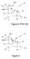
- FIG. 2is a circuit diagram of an active pixel sensor (APS) circuit
- FIG. 3is a circuit diagram of an active pixel sensor (APS) circuit in accordance with one embodiment of this invention.
- FIG. 4is a block diagram of an image sensor array in accordance with one embodiment of this invention.
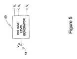
- FIG. 5is a schematic diagram of a multi-level voltage source used with the present invention.
- FIG. 6is illustrates reset voltages and reset voltage enable signals used in the preferred embodiment of the present invention.
- FIG. 1there is shown a block diagram of a typical image sensor array 10 .
- the sensor array 10consists of active pixel sensor (APS) circuits 11 arranged in rows 1 to n and columns 1 to m.
- the columns 1 to m of APS circuits 11are provided a voltage Vdd from a voltage supply 12 through lines VR 1 to VR m .
- each row 1 to n of APS circuits 11receive reset enable signals RRE 1 to RRE n which are normally pulses of equal amplitude but spaced in time from a row reset control 13 on lines 14 1 to 14 n to reset the sensor circuits 11 .
- Access to each horizontal row 1 to n of APS circuits 11is provided by applying individual access signals RA 1 to RA n which are normally pulses of equal amplitude but spaced in time via row lines 15 1 to l 5 n from a row address decoder 16 .
- the columns 1 to m of APS circuits 11are connected via data lines DL 1 to DL m which are coupled to column sense amplifiers 17 to amplify the image signal.
- the rows 1 to n of circuits 11are sequentially reset by signals RRE 1 to RRE n to detect the incident light on the circuits 11 whereas the sequential sensing of the level of incident light in the rows 1 to n of circuits 11 is initiated by access signals RA 1 to RA n and received on data lines DL 1 to DL m .
- FIG. 2A typical three transistor APS circuit 11 is illustrated in FIG. 2 .
- the circuit 11consists of a photodiode 21 coupled to the source of a reset transistor 22 and the gate of a transistor 23 which acts as a source follower amplifier.
- the drains of the reset transistor 22 and the amplifying transistor 23are normally connected to a supply voltage Vdd through a reset voltage line VR m .
- the amplifying transistor 23 sourceis coupled to a data line DL m through an access transistor 24 .
- the reset transistor 22places charge on one node 25 of the photodiode 21 from the supply voltage Vdd. This charge is drained through the photodiode 21 at a rate proportional to the intensity of incident light on the photodiode 21 .
- a signal proportional to this intensitycan be read from the circuit 11 on the dataline DL m by enabling the access transistor 24 .
- the timing for resetting the circuit 11 and then for accessing circuit 11is controlled by signals RRE n applied to reset transistors 22 and by signal RA n applied to transistor 24 .
- the period of time between the two signalswill be determined by the type of readout required for a specific application intended for the image sensor array 10 .
- the voltage Vdd supplied to the drain of the reset transistor 22is common to every circuit 11 (i.e. pixel) in the array 10 .
- Each row 1 to n of circuitsreceives a reset enable signal RRE 1 to RRE n respectively via a row reset line 14 1 to 14 n .
- the reset enable signals RRE 1 to RRE nare active when at a logical high and all have the same amplitude which may be substantially at the level of the supply voltage Vdd.
- the voltage level associated with this logical highis common throughout the array. This means that all photodiodes 21 in circuits 11 in the array 10 are reset to the same level, ie the same amount of reset charge is placed on the node of the photodiode 21 for every circuit 11 .
- the common reset voltage Vddensures that each circuit 11 will respond in a similar manner if illuminated by light of a similar intensity. This is ideal for image capture operations but does not lend itself to the isolation of adjacent circuits as would be required if the array were to be tested electrically rather that optically.
- different reset voltagesare applied to the nodes 25 of the photodiodes 21 in at least adjacent sensor circuits 11 in the array 10 .
- a predetermined period of time after the reset voltage has been appliedthe voltage at each node 25 is sensed to determine its level.
- the detected level for each sensor circuit 11 which has been provided with its individual signaturemay then be compared to an expected signal level for that circuit to determine if the circuit is faulty.
- the detected levels for adjacent sensor circuits 11are identical or very similar, it will be an indication that they are shorted together.
- one way of implementing the present inventionis to provide different reset voltages to adjacent columns of sensor circuits 1 I 1 using lines VR 1 to VR m .
- the voltage to the drain of transistor 22 in adjacent columns 1 to mwould differ.
- the reset enable signal RRE 1 to RRE nwould be generated at different active voltage levels for adjacent rows 1 to n of sensor circuits 11 .
- the reset enable signals RRE 1 to RRE n applied to the gates 26 of transistors 22 in adjacent rows 1 to nwould result in different voltages being applied to nodes 22 in the sensor circuits in adjacent rows 1 to n.
- each sensor circuit 11will be reset to a different voltage level than its neighbors, ie the column neighbors will be different because of different reset voltages on lines VR 1 to VR m and the row neighbors will be different because of the reset enable signals RRE 1 to RRE n on reset lines 14 1 to 14 n Therefore, it may be determined if an individual sensor circuit 11 is faulty by comparing the value of the signal received from the sensor circuit 11 to an expected level. In addition, if any one or more of the column lines or row lines are open circuited, groups of sensor circuits will appear to be inoperative, analysis will determine the faulty line.
- the circuit 31is similar to the circuit 11 illustrated in FIG. 2 except that the drain of transistor 23 is connected to a supply voltage Vdd line 32 which is common to all of the circuits 31 in the sensor array 10 .
- FIG. 4illustrates a sensor array 40 that is similar to the array 10 in FIG. 1 wherein common elements are identified by common reference numbers.
- the sensor circuits 31are identified as the type of circuit illustrated in FIG. 3 where a separate supply voltage Vdd is applied to transistors 23 via lines 32 which is integrated on the chip but is not shown on FIG. 4 for clarity.
- FIG. 4further schematically illustrates the row reset control 13 which includes inverters 41 1 to 41 n adapted to generate reset enable signals RRE 1 to RRE n on reset lines 14 1 to 14 n respectively.
- the inverters 41 1 to 41 nare connected to voltage supply lines 42 1 to 42 n which determines the amplitude of the output signals RRE 1 to RRE n .
- all lines 42 1 to 42 n and VR 1 to VR mare laid out on the die and connected together to a common supply Vdd via a single bond pad.
- each of the lines 42 1 to 42 n and VR 1 to VR mmay be separate so that they may be connected to different voltage supplies to carry-out the testing of the array. This would require either a separate power supply pin for each voltage level, or number voltage generators or dividers integrated on the sensor array 40 chip. Such an implementation would result in a severe die area penalty.
- two voltage levels V 1 and V 2are applied to the column reset voltage lines VR 1 to VR m via lines 43 and 44 and two levels of voltage V 3 and V 4 are applied to the rows 42 1 to 42 n via lines 45 and 46 .
- These voltage signalsare illustrated in FIG. 6 .
- the embodimentmay be further simplified by applying the same two voltage levels V 1 and V 2 to the column voltage reset lines VR 1 to VR m by connecting lines 43 and 44 respectively as well as to the rows 42 1 to 42 n by connecting lines 45 and 46 respectively.
- one level V 1would be provided to the odd numbered rows 42 1 , 42 3 , . . . and columns VR 1 , VR 3 , . . .
- the second level V 2would be provided to the even numbered rows 42 2 , 42 4 , . . . and columns VR 2 , VR 4 , . . .
- other combinations of voltage levelsare also possible.
- the two voltage levels V 1 and V 2 of the preferred embodimentcan be provided by an external source through two bond pads where one pad is already connected to a regular supply voltage Vdd. Once tested, if it is concluded that the die is not defective, the pads can be shorted together for normal operation. When the die is configured as such, the array will then receive only a single supply voltage Vdd.
- a voltage level generator 50may be integrated on the die which would include a single bond pad 51 for an external power supply Vdd. Circuits for boosting voltage levels such as charge pumps and circuits for stepping down voltage levels are well known in the art. The generator could provide any number of output voltages required for the testing of the sensor array 40 .
- defectsare identified by comparing the signals received on data lines DL 1 to DL m to expected values.
- This comparisoncan be accomplished off chip by a test system; however, a comparison circuit 47 may be integrated on the chip to determine if the signals received on data lines DL 1 to DL m agree with the expected data. This would greatly reduce the amount of complexity required of the system used to test the die. When combined with on chip voltage generators, this circuitry could be used as part of a built in self test (BIST) function.
- BISTbuilt in self test
- the main advantage of the present inventionis the ease through which independent APS circuits 11 , 31 are tested.
- a further advantage of the present inventionis the minimization of peripheral circuitry necessary to distribute the differing voltages to adjacent rows and columns in the array.
- Yet another advantage of the current inventionis the ability to test all of the row lines and data lines on an individual basis, resulting in faster interpretation of faults which reduces the time required to correct problems.
- the built in self test (BIST) embodiment in accordance with this inventionlends itself to the possibility of using it for applications other than testing during manufacturing.
- One applicationcould be for an image sensor used in a system which is controlled remotely, potentially in a satellite or some other location requiring such control. If the system were to malfunction, the BIST capability would allow the operator to test the sensor to determine if the fault was with components of the image sensor or some other component in the system.
Landscapes
- Engineering & Computer Science (AREA)
- Multimedia (AREA)
- Signal Processing (AREA)
- Transforming Light Signals Into Electric Signals (AREA)
- Solid State Image Pick-Up Elements (AREA)
- Light Receiving Elements (AREA)
Abstract
Description
Claims (18)
Priority Applications (4)
| Application Number | Priority Date | Filing Date | Title |
|---|---|---|---|
| US09/538,905US6489798B1 (en) | 2000-03-30 | 2000-03-30 | Method and apparatus for testing image sensing circuit arrays |
| CA002340572ACA2340572C (en) | 2000-03-30 | 2001-03-13 | Method and apparatus for testing image sensing circuit arrays |
| EP01302455AEP1143709A3 (en) | 2000-03-30 | 2001-03-16 | Method and apparatus for testing image sensing devices |
| JP2001097888AJP4979159B2 (en) | 2000-03-30 | 2001-03-30 | Method and apparatus for testing an image detection circuit array |
Applications Claiming Priority (1)
| Application Number | Priority Date | Filing Date | Title |
|---|---|---|---|
| US09/538,905US6489798B1 (en) | 2000-03-30 | 2000-03-30 | Method and apparatus for testing image sensing circuit arrays |
Publications (1)
| Publication Number | Publication Date |
|---|---|
| US6489798B1true US6489798B1 (en) | 2002-12-03 |
Family
ID=24148910
Family Applications (1)
| Application Number | Title | Priority Date | Filing Date |
|---|---|---|---|
| US09/538,905Expired - LifetimeUS6489798B1 (en) | 2000-03-30 | 2000-03-30 | Method and apparatus for testing image sensing circuit arrays |
Country Status (4)
| Country | Link |
|---|---|
| US (1) | US6489798B1 (en) |
| EP (1) | EP1143709A3 (en) |
| JP (1) | JP4979159B2 (en) |
| CA (1) | CA2340572C (en) |
Cited By (38)
| Publication number | Priority date | Publication date | Assignee | Title |
|---|---|---|---|---|
| US20030112028A1 (en)* | 2000-03-10 | 2003-06-19 | Ute Kollmer | Test circuit arrangement and method for testing a multiplicity of transistors |
| US6734897B1 (en)* | 1999-08-10 | 2004-05-11 | Agilent Technologies, Inc | Digital imaging circuit and method |
| US20040222812A1 (en)* | 2003-03-21 | 2004-11-11 | Gerd Frankowsky | Integrated circuit having a test circuit |
| US20040233324A1 (en)* | 2001-05-29 | 2004-11-25 | Transchip, Inc. | Systems and methods for power conservation in a CMOS imager |
| US20050068436A1 (en)* | 2001-05-29 | 2005-03-31 | Miriam Fraenkel | CMOS imager for cellular applications and methods of using such |
| DE102004020331B3 (en)* | 2004-04-26 | 2005-10-20 | Pilz Gmbh & Co Kg | Apparatus and method for capturing an image |
| US20060161827A1 (en)* | 2004-12-30 | 2006-07-20 | Teradyne, Inc. | Over-voltage test for automatic test equipment |
| US7086595B2 (en) | 2003-11-13 | 2006-08-08 | Metrologic Instruments, Inc. | Method of and apparatus for processing captured digital images of objects within a semi-automatic hand-supportable imaging-based bar code symbol reader so as to read 1d and/or 2d bar code symbols graphically represented therein |
| US20070138375A1 (en)* | 2005-12-19 | 2007-06-21 | Samsung Electronics Co. Ltd. | Image sensor, test system and test method for the same |
| US20070145983A1 (en)* | 2005-12-22 | 2007-06-28 | Semiconductor Manufacturing International (Shanghai) Corporation | Method and system for device characterization with array and decoder |
| US7270272B2 (en) | 2003-11-13 | 2007-09-18 | Metrologic Instruments, Inc. | Digital image-based bar code symbol reading system employing a multi-mode image-processing symbol reading subsystem |
| US7347374B2 (en) | 2003-11-13 | 2008-03-25 | Metrologic Instruments, Inc. | Hand-supportable digital imaging-based bar code symbol reader employing an event-driven system control subsystem, automatic IR-based object detection, and trigger-switch activated image capture and processing subsystem |
| US20080158363A1 (en)* | 2006-12-28 | 2008-07-03 | Micron Technology, Inc. | On-chip test system and method for active pixel sensor arrays |
| CN100424880C (en)* | 2004-09-17 | 2008-10-08 | 株式会社东芝 | Semiconductor optical sensing device and information equipment |
| US20080303905A1 (en)* | 2007-06-08 | 2008-12-11 | Micron Technology, Inc. | Methods and apparatuses for non-optical pixel self test |
| US7464877B2 (en) | 2003-11-13 | 2008-12-16 | Metrologic Instruments, Inc. | Digital imaging-based bar code symbol reading system employing image cropping pattern generator and automatic cropped image processor |
| US20090066793A1 (en)* | 2005-05-11 | 2009-03-12 | Matsushita Electric Industrial Co., Ltd. | Solid-state imaging device, camera, automobile and monitoring device |
| US7513428B2 (en) | 2001-11-21 | 2009-04-07 | Metrologic Instruments, Inc. | Planar laser illumination and imaging device employing laser current modulation to generate spectral components and reduce temporal coherence of laser beam, so as to achieve a reduction in speckle-pattern noise during time-averaged detection of images of objects illuminated thereby during imaging operations |
| US7516898B2 (en) | 2000-11-24 | 2009-04-14 | Metrologic Instruments, Inc. | Digital image capturing and processing system for producing and projecting a complex of coplanar illumination and imaging planes into a 3D imaging volume and controlling illumination control parameters in said system using the detected motion and velocity of object |
| US7523863B2 (en) | 1999-06-07 | 2009-04-28 | Metrologic Instruments, Inc. | Hand-supportable LED-based planar illumination and imaging system |
| US7527200B2 (en) | 1998-03-24 | 2009-05-05 | Metrologic Instruments, Inc. | Planar laser illumination and imaging (PLIIM) systems with integrated despeckling mechanisms provided therein |
| US7527202B2 (en) | 2000-06-07 | 2009-05-05 | Metrologic Instruments, Inc. | Hand-supportable planar linear illumination and imaging (PLIIM) based code symbol reading system |
| US7546952B2 (en) | 2000-11-24 | 2009-06-16 | Metrologic Instruments, Inc. | Method of illuminating objects during digital image capture operations by mixing visible and invisible spectral illumination energy at point of sale (POS) environments |
| US20090160752A1 (en)* | 2007-12-21 | 2009-06-25 | Guy Meynants | Pixel array with reduced sensitivity to defects |
| US20090237103A1 (en)* | 2008-03-20 | 2009-09-24 | International Business Machines Corporation | Image sensor monitor structure in scribe area |
| US7594609B2 (en) | 2003-11-13 | 2009-09-29 | Metrologic Instruments, Inc. | Automatic digital video image capture and processing system supporting image-processing based code symbol reading during a pass-through mode of system operation at a retail point of sale (POS) station |
| US7607581B2 (en) | 2003-11-13 | 2009-10-27 | Metrologic Instruments, Inc. | Digital imaging-based code symbol reading system permitting modification of system features and functionalities |
| US7708205B2 (en) | 2003-11-13 | 2010-05-04 | Metrologic Instruments, Inc. | Digital image capture and processing system employing multi-layer software-based system architecture permitting modification and/or extension of system features and functions by way of third party code plug-ins |
| US7841533B2 (en) | 2003-11-13 | 2010-11-30 | Metrologic Instruments, Inc. | Method of capturing and processing digital images of an object within the field of view (FOV) of a hand-supportable digitial image capture and processing system |
| US20110253999A1 (en)* | 2010-04-15 | 2011-10-20 | Texas Instruments Incorporated | Semiconductor wafer having scribe line test modules including matching portions from subcircuits on active die |
| CN102680884A (en)* | 2012-05-18 | 2012-09-19 | 北京大学 | Circuit for measuring characteristics of large-scale array device |
| US9007078B2 (en) | 2012-04-06 | 2015-04-14 | Industrial Technology Research Institute | Pixel array module with self-test function and method thereof |
| US20150281684A1 (en)* | 2014-03-31 | 2015-10-01 | Semiconductor Components Industries, Llc | Imaging systems with pixel array verification circuitry |
| CN111277776A (en)* | 2015-04-10 | 2020-06-12 | 三星电子株式会社 | Image Sensor |
| US10949634B2 (en) | 2005-06-03 | 2021-03-16 | Hand Held Products, Inc. | Apparatus having hybrid monochrome and color image sensor array |
| US11317050B2 (en) | 2005-03-11 | 2022-04-26 | Hand Held Products, Inc. | Image reader comprising CMOS based image sensor array |
| US11327476B2 (en)* | 2018-11-13 | 2022-05-10 | Microsoft Technology Licensing, Llc | Sensor fall curve identification |
| WO2025061857A1 (en) | 2023-09-20 | 2025-03-27 | Trinamix Gmbh | Automated out-of-line pixel detection |
Families Citing this family (12)
| Publication number | Priority date | Publication date | Assignee | Title |
|---|---|---|---|---|
| TW552799B (en)* | 2000-10-03 | 2003-09-11 | Agilent Technologies Inc | System solution for amorphous lag problem |
| KR100477785B1 (en)* | 2002-04-27 | 2005-03-22 | 매그나칩 반도체 유한회사 | CMOS image sensor with test Pattern for evaluating characteristics |
| JP2007333823A (en)* | 2006-06-13 | 2007-12-27 | Sony Corp | Liquid crystal display device and inspection method for liquid crystal display device |
| JP2009059811A (en)* | 2007-08-30 | 2009-03-19 | Sharp Corp | Solid-state imaging device and electronic information device |
| US8599307B2 (en)* | 2011-07-25 | 2013-12-03 | Aptina Imaging Corporation | Method and apparatus for rapid verification of imaging systems |
| DE102011087133B4 (en)* | 2011-11-25 | 2020-02-27 | pmdtechnologies ag | Device and method for monitoring global pixel control |
| JP5926980B2 (en)* | 2012-02-27 | 2016-05-25 | オリンパス株式会社 | Imaging apparatus and imaging system |
| CN104271027B (en)* | 2012-06-27 | 2017-06-23 | 奥林巴斯株式会社 | Camera head and camera system |
| KR102379807B1 (en)* | 2015-12-31 | 2022-03-29 | 엘지디스플레이 주식회사 | Organic light emitting display device and the method for driving the same |
| JP6932542B2 (en)* | 2017-05-09 | 2021-09-08 | キヤノン株式会社 | Imaging device, imaging system and mobile |
| JP7066342B2 (en) | 2017-06-29 | 2022-05-13 | キヤノン株式会社 | Imaging device, imaging system, moving object |
| JP6812397B2 (en)* | 2018-11-14 | 2021-01-13 | キヤノン株式会社 | Solid-state image sensor, its driving method, and image sensor |
Citations (8)
| Publication number | Priority date | Publication date | Assignee | Title |
|---|---|---|---|---|
| US5153421A (en)* | 1991-11-04 | 1992-10-06 | Xerox Corporation | Architecture for analog and digital image sensor arrays |
| US5276400A (en) | 1989-09-23 | 1994-01-04 | University Of Edinburgh | Test circuit for imaging sensing integrated circuits |
| US5451768A (en) | 1994-11-14 | 1995-09-19 | Xerox Corporation | On-chip test circuit and method for an image sensor array |
| US5654537A (en) | 1995-06-30 | 1997-08-05 | Symbios Logic Inc. | Image sensor array with picture element sensor testability |
| US5721422A (en)* | 1995-03-16 | 1998-02-24 | U.S. Philips Corporation | Electronic devices having an array with shared column conductors |
| US5896173A (en)* | 1995-07-07 | 1999-04-20 | Siemens Aktiengesellschaft | Image detector with selective readout of pixels in groups or individually |
| US5898168A (en)* | 1997-06-12 | 1999-04-27 | International Business Machines Corporation | Image sensor pixel circuit |
| US6028299A (en)* | 1995-12-05 | 2000-02-22 | Sony Corporation | Linear image sensor device comprising first and second linear image sensor sections having first and second sensitivities |
Family Cites Families (4)
| Publication number | Priority date | Publication date | Assignee | Title |
|---|---|---|---|---|
| JPH06164828A (en)* | 1992-11-24 | 1994-06-10 | Fuji Xerox Co Ltd | Drive method for image sensor |
| JPH1197658A (en)* | 1997-09-16 | 1999-04-09 | Nikon Corp | Sensor device and inspection method thereof |
| US6118482A (en)* | 1997-12-08 | 2000-09-12 | Intel Corporation | Method and apparatus for electrical test of CMOS pixel sensor arrays |
| JP2000244005A (en)* | 1999-02-24 | 2000-09-08 | Canon Inc | Photoelectric conversion device |
- 2000
- 2000-03-30USUS09/538,905patent/US6489798B1/ennot_activeExpired - Lifetime
- 2001
- 2001-03-13CACA002340572Apatent/CA2340572C/ennot_activeExpired - Fee Related
- 2001-03-16EPEP01302455Apatent/EP1143709A3/ennot_activeWithdrawn
- 2001-03-30JPJP2001097888Apatent/JP4979159B2/ennot_activeExpired - Lifetime
Patent Citations (8)
| Publication number | Priority date | Publication date | Assignee | Title |
|---|---|---|---|---|
| US5276400A (en) | 1989-09-23 | 1994-01-04 | University Of Edinburgh | Test circuit for imaging sensing integrated circuits |
| US5153421A (en)* | 1991-11-04 | 1992-10-06 | Xerox Corporation | Architecture for analog and digital image sensor arrays |
| US5451768A (en) | 1994-11-14 | 1995-09-19 | Xerox Corporation | On-chip test circuit and method for an image sensor array |
| US5721422A (en)* | 1995-03-16 | 1998-02-24 | U.S. Philips Corporation | Electronic devices having an array with shared column conductors |
| US5654537A (en) | 1995-06-30 | 1997-08-05 | Symbios Logic Inc. | Image sensor array with picture element sensor testability |
| US5896173A (en)* | 1995-07-07 | 1999-04-20 | Siemens Aktiengesellschaft | Image detector with selective readout of pixels in groups or individually |
| US6028299A (en)* | 1995-12-05 | 2000-02-22 | Sony Corporation | Linear image sensor device comprising first and second linear image sensor sections having first and second sensitivities |
| US5898168A (en)* | 1997-06-12 | 1999-04-27 | International Business Machines Corporation | Image sensor pixel circuit |
Cited By (208)
| Publication number | Priority date | Publication date | Assignee | Title |
|---|---|---|---|---|
| US7527200B2 (en) | 1998-03-24 | 2009-05-05 | Metrologic Instruments, Inc. | Planar laser illumination and imaging (PLIIM) systems with integrated despeckling mechanisms provided therein |
| US7523863B2 (en) | 1999-06-07 | 2009-04-28 | Metrologic Instruments, Inc. | Hand-supportable LED-based planar illumination and imaging system |
| US7533821B2 (en) | 1999-06-07 | 2009-05-19 | Metrologic Instruments, Inc. | Hand-supportable planar laser illumination and imaging (PLIIM) device for producing a planar laser illumination beam (PLIB) coplanar with the field of view (FOV) of a linear image detection array |
| US7621455B2 (en) | 1999-06-07 | 2009-11-24 | Metrologic Instruments, Inc. | Hand-supportable code symbol reader employing coplanar laser illumination and linear imaging |
| US7644866B2 (en) | 1999-06-07 | 2010-01-12 | Metrologic Instruments, Inc. | Hand-supportable code symbol reader employing coplanar laser illumination and linear imaging |
| US6734897B1 (en)* | 1999-08-10 | 2004-05-11 | Agilent Technologies, Inc | Digital imaging circuit and method |
| US6873173B2 (en)* | 2000-03-10 | 2005-03-29 | Infineon Technologies Ag | Test circuit arrangement and method for testing a multiplicity of transistors |
| US20030112028A1 (en)* | 2000-03-10 | 2003-06-19 | Ute Kollmer | Test circuit arrangement and method for testing a multiplicity of transistors |
| US7527202B2 (en) | 2000-06-07 | 2009-05-05 | Metrologic Instruments, Inc. | Hand-supportable planar linear illumination and imaging (PLIIM) based code symbol reading system |
| US7793841B2 (en) | 2000-11-24 | 2010-09-14 | Metrologic Instruments, Inc. | Laser illumination beam generation system employing despeckling of the laser beam using high-frequency modulation of the laser diode current and optical multiplexing of the component laser beams |
| US7540424B2 (en) | 2000-11-24 | 2009-06-02 | Metrologic Instruments, Inc. | Compact bar code symbol reading system employing a complex of coplanar illumination and imaging stations for omni-directional imaging of objects within a 3D imaging volume |
| US7819326B2 (en) | 2000-11-24 | 2010-10-26 | Metrologic Instruments, Inc. | Network of digital image capturing systems installed at retail POS-based stations and serviced by a remote image processing server in communication therewith |
| US7815113B2 (en) | 2000-11-24 | 2010-10-19 | Metrologic Instruments, Inc. | Method of and system for returning a consumer product in a retail environment so as to prevent or reduce employee theft, as well as provide greater accountability for returned merchandise in retail store environments |
| US7806336B2 (en) | 2000-11-24 | 2010-10-05 | Metrologic Instruments, Inc. | Laser beam generation system employing a laser diode and high-frequency modulation circuitry mounted on a flexible circuit |
| US7806335B2 (en) | 2000-11-24 | 2010-10-05 | Metrologic Instruments, Inc. | Digital image capturing and processing system for automatically recognizing objects in a POS environment |
| US7905413B2 (en) | 2000-11-24 | 2011-03-15 | Metrologic Instruments, Inc. | Digital image capturing and processing system employing a plurality of coplanar illumination and imaging subsystems for digitally imaging objects in a 3D imaging volume, and a globally-deployed object motion detection subsystem for automatically detecting and analyzing the motion of objects passing through said 3-D imaging volume |
| US7784695B2 (en) | 2000-11-24 | 2010-08-31 | Metrologic Instruments, Inc. | Planar laser illumination module (PLIM) employing high-frequency modulation (HFM) of the laser drive currents and optical multplexing of the output laser beams |
| US7775436B2 (en) | 2000-11-24 | 2010-08-17 | Metrologic Instruments, Inc. | Method of driving a plurality of visible and invisible LEDs so as to produce an illumination beam having a dynamically managed ratio of visible to invisible (IR) spectral energy/power during object illumination and imaging operations |
| US7770796B2 (en) | 2000-11-24 | 2010-08-10 | Metrologic Instruments, Inc. | Device for producing a laser beam of reduced coherency using high-frequency modulation of the laser diode current and optical multiplexing of the output laser beam |
| US7762465B2 (en) | 2000-11-24 | 2010-07-27 | Metrologic Instruments, Inc. | Device for optically multiplexing a laser beam |
| US7520433B2 (en) | 2000-11-24 | 2009-04-21 | Metrologic Instruments, Inc. | Method for intelligently controlling the illumination and imagine of objects as they are moved through the 3D imaging volume of a digital image capturing and processing system |
| US7731091B2 (en) | 2000-11-24 | 2010-06-08 | Metrologic Instruments, Inc. | Digital image capturing and processing system employing automatic object detection and spectral-mixing based illumination techniques |
| US7516898B2 (en) | 2000-11-24 | 2009-04-14 | Metrologic Instruments, Inc. | Digital image capturing and processing system for producing and projecting a complex of coplanar illumination and imaging planes into a 3D imaging volume and controlling illumination control parameters in said system using the detected motion and velocity of object |
| US7673802B2 (en) | 2000-11-24 | 2010-03-09 | Metrologic Instruments, Inc. | Automatic POS-based digital image capturing and processing system employing a plurality of area-type illumination and imaging zones intersecting within the 3D imaging volume of the system |
| US7527204B2 (en) | 2000-11-24 | 2009-05-05 | Metrologic Instruments, Inc. | Omni-directional digital image capturing and processing system comprising coplanar illumination and imaging stations automatically detecting object motion and velocity and adjusting exposure and/or illumination control parameters therewithin |
| US7665665B2 (en) | 2000-11-24 | 2010-02-23 | Metrologic Instruments, Inc. | Digital illumination and imaging subsystem employing despeckling mechanism employing high-frequency modulation of laser diode drive current and optical beam multiplexing techniques |
| US7661595B2 (en) | 2000-11-24 | 2010-02-16 | Metrologic Instruments, Inc. | Digital image capturing and processing system employing a plurality of area-type illuminating and imaging stations projecting a plurality of coextensive area-type illumination and imaging zones into a 3D imaging volume, and controlling operations therewithin using |
| US7661597B2 (en) | 2000-11-24 | 2010-02-16 | Metrologic Instruments, Inc. | Coplanar laser illumination and imaging subsystem employing spectral-mixing and despeckling of laser illumination |
| US7658330B2 (en) | 2000-11-24 | 2010-02-09 | Metrologic Instruments, Inc. | Automatic POS-based digital image capturing and processing system employing object motion controlled area-type illumination and imaging operations |
| US7651028B2 (en) | 2000-11-24 | 2010-01-26 | Metrologic Instruments, Inc. | Intelligent system for automatically recognizing objects at a point of sale (POS) station by omni-directional imaging of the objects using a complex of coplanar illumination and imaging subsystems |
| US8042740B2 (en) | 2000-11-24 | 2011-10-25 | Metrologic Instruments, Inc. | Method of reading bar code symbols on objects at a point-of-sale station by passing said objects through a complex of stationary coplanar illumination and imaging planes projected into a 3D imaging volume |
| US8172141B2 (en) | 2000-11-24 | 2012-05-08 | Metrologic Instruments, Inc. | Laser beam despeckling devices |
| US7614560B2 (en) | 2000-11-24 | 2009-11-10 | Metrologic Instruments, Inc. | Method of illuminating objects at a point of sale (POS) station by adaptively controlling the spectral composition of the wide-area illumination beam produced from an illumination subsystem within an automatic digital image capture and processing system |
| US7611062B2 (en) | 2000-11-24 | 2009-11-03 | Metrologic Instruments, Inc. | Omni-directional digital image capturing and processing system employing coplanar illumination and imaging planes and area-type illumination and imaging zones with the horizontal and vertical sections of the system housing |
| US7594608B2 (en) | 2000-11-24 | 2009-09-29 | Metrologic Instruments, Inc. | Automatic omnidirectional bar code symbol reading system employing linear-type and area-type bar code symbol reading stations within the system housing |
| US7588188B2 (en) | 2000-11-24 | 2009-09-15 | Metrologic Instruments, Inc. | Pos-based digital image capturing and processing system using automatic object detection, spectral-mixing based illumination and linear imaging techniques |
| US7584892B2 (en) | 2000-11-24 | 2009-09-08 | Metrologic Instruments, Inc. | Digital-imaging based code symbol reading system employing a plurality of coplanar illumination and imaging subsystems, each having a local object motion detection subsystem for automatic detecting objects within the 3D imaging volume, and a local control subsystem for transmitting object detection state data to a global control subsystem for managing the state of operation of said coplanar illumination and imaging subsystems |
| US7581680B2 (en) | 2000-11-24 | 2009-09-01 | Metrologic Instruments, Inc. | Omni-directional digital image capturing and processing system employing coplanar illumination and imaging stations in horizontal and vertical housing sections of the system |
| US7578442B2 (en) | 2000-11-24 | 2009-08-25 | Metrologic Instruments, Inc. | Method of and apparatus for identifying consumer products in a retail environment when bar code symbols on the products are not readable or have been removed from packaging |
| US7578445B2 (en) | 2000-11-24 | 2009-08-25 | Metrologic Instruments, Inc. | Automatic POS-based digital image capturing and processing system employing object motion controlled area-type illumination and imaging operations |
| US7575170B2 (en) | 2000-11-24 | 2009-08-18 | Metrologic Instruments, Inc. | POS-based digital image capturing and processing system using automatic object detection, spectral-mixing based illumination and linear imaging techniques |
| US7575169B2 (en) | 2000-11-24 | 2009-08-18 | Metrologic Instruments, Inc. | Digital image capturing and processing system for producing and projecting a plurality of coextensive area-type illumination and imaging zones into a 3D imaging volume and controlling illumination control parameters in said system using the detected motion of objects present therewithin |
| US7571859B2 (en) | 2000-11-24 | 2009-08-11 | Metrologic Instruments, Inc. | Digital-imaging based code symbol reading system employing a plurality of coplanar illumination and imaging subsystems, global object motion detection subsystem for automatically detecting objects within its 3D imaging volume, and global control subsystem for managing the state of operation of said coplanar illumination and imaging substems |
| US7571858B2 (en) | 2000-11-24 | 2009-08-11 | Metrologic Instruemtns, Inc. | POS-based digital image capturing and processing system using automatic object detection, spectral-mixing based illumination and linear imaging techniques |
| US7568626B2 (en) | 2000-11-24 | 2009-08-04 | Metrologic Instruments, Inc. | Automatic POS-based digital image capturing and processing system employing a plurality of area-type illumination and imaging zones intersecting within the 3D imaging volume of the system |
| US7559474B2 (en) | 2000-11-24 | 2009-07-14 | Metrologic Instruments, Inc. | Automatic omnidirectional bar code symbol reading system employing linear-type and area-type bar code symbol reading stations within the system housing |
| US7556199B2 (en) | 2000-11-24 | 2009-07-07 | Metrologic Instruments, Inc. | Digital image capturing and processing system employing a plurality of coplanar illuminating and imaging stations projecting a complex of coplanar illumination and imaging planes into a 3D imaging volume so as to support pass-through and presentation modes of digital imaging at a point of sale (POS) environment |
| US7546952B2 (en) | 2000-11-24 | 2009-06-16 | Metrologic Instruments, Inc. | Method of illuminating objects during digital image capture operations by mixing visible and invisible spectral illumination energy at point of sale (POS) environments |
| US7543749B2 (en) | 2000-11-24 | 2009-06-09 | Metrologic Instruments, Inc. | Digital image capturing and processing system having a plurality of coplanar illumination and imaging subsystems, each employing a dual-type coplanar linear illumination and imaging engine that supports image-processing based object motion and velocity detection, and automatic image formation and detection along the coplanar illumination and imaging plane produced thereby |
| US7878407B2 (en) | 2000-11-24 | 2011-02-01 | Metrologic Instruments, Inc. | POS-based digital image capturing and processing system employing automatic object motion detection and spectral-mixing based illumination techniques |
| US7540422B2 (en) | 2000-11-24 | 2009-06-02 | Metrologic Instruments, Inc. | Digital image capturing and processing system employing imaging window protection plate having an aperture pattern and being disposed over said imaging window and beneath which resides a plurality of coplanar illumination and imaging stations |
| US7537165B2 (en) | 2000-11-24 | 2009-05-26 | Metrologic Instruments, Inc. | Omni-directional digital image capturing and processing system employing coplanar illumination and imaging planes and area-type illumination and imaging zones within the system housing |
| US7530497B2 (en) | 2000-11-24 | 2009-05-12 | Metrologic Instruments, Inc. | Digital image capturing and processing system employing an image capturing and processing module and an integrated electronic weigh scale module having a load cell centrally located with respect to said image capturing and processing module |
| US7533820B2 (en) | 2000-11-24 | 2009-05-19 | Metrologic Instruments, Inc. | Digital image capturing and processing system employing coplanar illumination and imaging stations which generate coplanar illumination and imaging planes only when and where an object is being moved within the 3D imaging volume |
| US7533823B2 (en) | 2000-11-24 | 2009-05-19 | Metrologic Instruments, Inc. | Digital image capturing and processing system employing a plurality of coplanar illuminating and imaging stations projecting a plurality of coplanar illumination and imaging planes into a 3D imaging volume, and controlling operations therewithin using control data derived from motion data collected from the automated detection of objects passing through said 3D imaging volume |
| US20050068436A1 (en)* | 2001-05-29 | 2005-03-31 | Miriam Fraenkel | CMOS imager for cellular applications and methods of using such |
| US20050128325A1 (en)* | 2001-05-29 | 2005-06-16 | Miriam Fraenkel | Built-in self test for a CMOS imager |
| US7667751B2 (en)* | 2001-05-29 | 2010-02-23 | Samsung Electronics Co., Ltd. | Built-in self test for a CMOS imager |
| US7701497B2 (en) | 2001-05-29 | 2010-04-20 | Samsung Electronics Co., Ltd. | CMOS imager for cellular applications and methods of using such |
| US7738013B2 (en) | 2001-05-29 | 2010-06-15 | Samsung Electronics Co., Ltd. | Systems and methods for power conservation in a CMOS imager |
| US20040233324A1 (en)* | 2001-05-29 | 2004-11-25 | Transchip, Inc. | Systems and methods for power conservation in a CMOS imager |
| US7513428B2 (en) | 2001-11-21 | 2009-04-07 | Metrologic Instruments, Inc. | Planar laser illumination and imaging device employing laser current modulation to generate spectral components and reduce temporal coherence of laser beam, so as to achieve a reduction in speckle-pattern noise during time-averaged detection of images of objects illuminated thereby during imaging operations |
| US20040222812A1 (en)* | 2003-03-21 | 2004-11-11 | Gerd Frankowsky | Integrated circuit having a test circuit |
| US7494063B2 (en) | 2003-11-13 | 2009-02-24 | Metrologic Instruments, Inc. | Automatic imaging-based code symbol reading system supporting a multi-tier modular software architecture, automatic illumination control, and video image capture and processing techniques |
| US7815121B2 (en) | 2003-11-13 | 2010-10-19 | Metrologic Instruments, Inc. | Method of modifying and/or extending the standard features and functions of a digital image capture and processing system |
| US9785811B2 (en) | 2003-11-13 | 2017-10-10 | Metrologic Instruments, Inc. | Image capture and processing system supporting a multi-tier modular software architecture |
| US7513430B2 (en) | 2003-11-13 | 2009-04-07 | Metrologic Instruments, Inc. | Digital image capturing and processing system employing an area-type image sensing array exposed to narrow-band illumination from a narrow-band illumination subsystem for a time duration controlled using a photodetector operated independently from said area-type image sensing array |
| US7510122B2 (en) | 2003-11-13 | 2009-03-31 | Metrologic Instruments, Inc. | Portable digital image capturing and processing system employing an area-type image sensing array exposed to illumination produced from an LED-based illumination array and measured using a photodector operated independently from said area-type image sensing array |
| US7503498B2 (en) | 2003-11-13 | 2009-03-17 | Metrologic Instruments, Inc. | Hand-supportable digital image capturing and processing system employing an area-type image sensing array exposed to illumination from an LED-based illumination array only when all sensor elements in said image-sensing array are activated and in a state of integration |
| US7503499B2 (en) | 2003-11-13 | 2009-03-17 | Metrologic Instruments, Inc. | Digital image capturing and processing system producing narrow-band illumination when image sensor elements in a state of integration, and simultaneously detecting narrow-band illumination using an area-type image sensor and independently-operated photo-detector |
| US9355288B2 (en) | 2003-11-13 | 2016-05-31 | Metrologic Instruments, Inc. | Image capture and processing system supporting a multi-tier modular software architecture |
| US7490778B2 (en) | 2003-11-13 | 2009-02-17 | Metrologic Instruments, Inc. | Method of reading code symbols using a hand-supportable digital image capturing and processing device employing a micro-computing platform supporting an event-driven multi-tier modular software architecture |
| US7490774B2 (en) | 2003-11-13 | 2009-02-17 | Metrologic Instruments, Inc. | Hand-supportable imaging based bar code symbol reader employing automatic light exposure measurement and illumination control subsystem integrated therein |
| US7540425B2 (en) | 2003-11-13 | 2009-06-02 | Metrologic Instruments, Inc. | Method of dynamically controlling illumination and image capturing operations in a digital image capture and processing system |
| US7487917B2 (en) | 2003-11-13 | 2009-02-10 | Metrologic Instruments, Inc. | Automatic digital-imaging based code symbol reading system supporting pass-through and presentation modes of system operation using automatic object direction detection, narrow-area and wide-area illumination control, and narrow-area and wide-area video image capture and processing techniques |
| US9104930B2 (en) | 2003-11-13 | 2015-08-11 | Metrologic Instruments, Inc. | Code symbol reading system |
| US7484666B2 (en) | 2003-11-13 | 2009-02-03 | Metrologic Instruments, Inc. | Automatic digital-imaging based bar code symbol reading system supporting pass-through and presentation modes of system operation using automatic object direction detection and illumination control, and video image capture and processing techniques |
| US7543752B2 (en) | 2003-11-13 | 2009-06-09 | Metrologic Instruments, Inc. | Digital image capture and processing system employing a multi-mode illumination subsystem adaptable to ambient illumination levels |
| US7469835B2 (en) | 2003-11-13 | 2008-12-30 | Metrologic Instruments, Inc. | Digital-imaging based code symbol reading system employing an event-driven multi-tier modular software architecture and supporting automatic operating system login and loading of code symbol reading application |
| US7546951B2 (en) | 2003-11-13 | 2009-06-16 | Meterologic Instruments, Inc. | Digital image capture and processing system employing real-time analysis of image exposure quality and the reconfiguration of system control parameters based on the results of such exposure quality analysis |
| US8844822B2 (en) | 2003-11-13 | 2014-09-30 | Metrologic Instruments, Inc. | Image capture and processing system supporting a multi-tier modular software architecture |
| US7464877B2 (en) | 2003-11-13 | 2008-12-16 | Metrologic Instruments, Inc. | Digital imaging-based bar code symbol reading system employing image cropping pattern generator and automatic cropped image processor |
| US7559475B2 (en) | 2003-11-13 | 2009-07-14 | Metrologic Instruments, Inc. | Automatic digital-imaging based bar code symbol reading system supporting a pass-through mode of system operation using automatic object direction detection and illumination control, and video image capture and processing techniques |
| US8479992B2 (en) | 2003-11-13 | 2013-07-09 | Metrologic Instruments, Inc. | Optical code symbol reading system employing an acoustic-waveguide structure for coupling sonic energy, produced from an electro-transducer, to sound wave ports formed in the system housing |
| US8366005B2 (en) | 2003-11-13 | 2013-02-05 | Metrologic Instruments, Inc. | Hand-supportable digital image capture and processing system supporting a multi-tier modular software architecture |
| US7568625B2 (en) | 2003-11-13 | 2009-08-04 | Metpologic Instruments, Inc. | Hand-supportable digital image-processing based bar code symbol reading system employing image cropping zone (ICZ) framing and post-image capture cropping |
| US7428998B2 (en) | 2003-11-13 | 2008-09-30 | Metrologic Instruments, Inc. | Automatic hand-supportable image-based bar code symbol reader having image-processing based bar code reading subsystem employing simple decode image processing operations applied in an outwardly-directed manner referenced from the center of a captured narrow-area digital image of an object bearing a 1D bar code symbol |
| US7407109B2 (en) | 2003-11-13 | 2008-08-05 | Metrologic Instruments, Inc. | Digital-imaging based code symbol reading system employing a micro-computing platform supporting an event-driven multi-tier modular software architecture |
| US7575167B2 (en) | 2003-11-13 | 2009-08-18 | Metrologic Instruments, Inc. | Method of dynamically managing system control parameters in a digital image capture and processing system |
| US8317105B2 (en) | 2003-11-13 | 2012-11-27 | Metrologic Instruments, Inc. | Optical scanning system having an extended programming mode and method of unlocking restricted extended classes of features and functionalities embodied therewithin |
| US8157175B2 (en) | 2003-11-13 | 2012-04-17 | Metrologic Instruments, Inc. | Digital image capture and processing system supporting a presentation mode of system operation which employs a combination of video and snapshot modes of image detection array operation during a single cycle of system operation |
| US8157174B2 (en) | 2003-11-13 | 2012-04-17 | Metrologic Instruments, Inc. | Digital image capture and processing system employing an image formation and detection system having an area-type image detection array supporting single snap-shot and periodic snap-shot modes of image acquisition during object illumination and imaging operations |
| US7360706B2 (en) | 2003-11-13 | 2008-04-22 | Metrologic Instruments, Inc. | Hand-supportable imaging-based auto-discriminating 1D/2D bar code symbol reader employing a multi-mode image processing bar code symbol reading subsystem having a plurality of modes of operation which are dynamically reconfigurable in response to real-time image analysis |
| US7357325B2 (en) | 2003-11-13 | 2008-04-15 | Metrologic Instruments, Inc. | Hand-supportable imaging-based bar code symbol reader employing a CMOS-type image sensor using global exposure techniques |
| US7347374B2 (en) | 2003-11-13 | 2008-03-25 | Metrologic Instruments, Inc. | Hand-supportable digital imaging-based bar code symbol reader employing an event-driven system control subsystem, automatic IR-based object detection, and trigger-switch activated image capture and processing subsystem |
| US7588190B2 (en) | 2003-11-13 | 2009-09-15 | Metrologic Instruments, Inc. | Digital-imaging code symbol reading system supporting automatic programming of system parameters for automatic configuration of said system in hands-on and hands-free modes of operation |
| US8132731B2 (en) | 2003-11-13 | 2012-03-13 | Metrologic Instruments, Inc. | Digital image capture and processing system having a printed circuit (PC) board with a light transmission aperture, wherein an image detection array is mounted on the rear side of said PC board, and a linear array of light emitting diodes (LEDS) is mounted on the front surface of said PC board, and aligned with an illumination-focusing lens structure integrated within said imaging window |
| US8100331B2 (en) | 2003-11-13 | 2012-01-24 | Metrologic Instruments, Inc. | Digital image capture and processing system having a printed circuit (PC) board with light transmission aperture, wherein first and second field of view (FOV) folding mirrors project the FOV of a digital image detection array on the rear surface of said PC board, through said light transmission aperture |
| US7594609B2 (en) | 2003-11-13 | 2009-09-29 | Metrologic Instruments, Inc. | Automatic digital video image capture and processing system supporting image-processing based code symbol reading during a pass-through mode of system operation at a retail point of sale (POS) station |
| US7325738B2 (en) | 2003-11-13 | 2008-02-05 | Metrologic Instruments, Inc. | Method of and system for determining the lower limit of decoding resolution in an imaging-based bar code symbol reader |
| US7604175B2 (en) | 2003-11-13 | 2009-10-20 | Metrologic Instruments, Inc. | Method of reading bar code symbols using a digital-imaging based code symbol reading system employing an event-driven multi-tier modular software architecture and supporting automatic operating system login and loading of bar code symbol reading application |
| US7607581B2 (en) | 2003-11-13 | 2009-10-27 | Metrologic Instruments, Inc. | Digital imaging-based code symbol reading system permitting modification of system features and functionalities |
| US7320431B2 (en) | 2003-11-13 | 2008-01-22 | Metrologic Instruments, Inc. | Digital imaging-based bar code symbol reading system employing a multi-mode illumination subsystem with far-field and near field led-based illumination arrays |
| US7611064B2 (en) | 2003-11-13 | 2009-11-03 | Metrologic Instruments, Inc. | Digital image capture and processing system having automatic illumination measurement and control capabilities realized using a photodetector operating independently of the image sensing array, and an image-processing based illumination metering program for automatically adjusting the illumination duration of the system during object illumination and imaging operations |
| US7299986B2 (en) | 2003-11-13 | 2007-11-27 | Metrologic Instruments, Inc. | Digital imaging-based bar code symbol driven portable data terminal system |
| US7293714B2 (en) | 2003-11-13 | 2007-11-13 | Metrologic Instruments, Inc. | Hand-supportable digital imaging-based bar code symbol reading system automatically processing captured images along parallel virtual scan lines based on the maximum pixel height of the region of interest (ROI) |
| US7624926B2 (en) | 2003-11-13 | 2009-12-01 | Metrologic Instruments, Inc. | Method of automatically reading code symbols on objects present within the field of view (FOV) of a hand-supportable digital-imaging based code symbol reader, by simultaneously projecting an image cropping zone (ICZ) framing pattern and a field of illumination within the FOV during object illumination and imaging operations |
| US8087588B2 (en) | 2003-11-13 | 2012-01-03 | Metrologic Instruments, Inc. | Digital image capture and processing system having a single printed circuit (PC) board with a light transmission aperture, wherein a first linear array of visible light emitting diodes (LEDs) are mounted on the rear side of the PC board for producing a linear targeting illumination beam, and wherein a second linear array of visible LEDs are mounted on the front side of said PC board for producing a field of visible illumination within the field of view (FOV) of the system |
| US7637432B2 (en) | 2003-11-13 | 2009-12-29 | Metrologic Instruments, Inc. | Automatic point-of-sale based code symbol reading system employing automatic object motion detection and illumination control, and digital video image capturing and processing techniques |
| US7637433B1 (en) | 2003-11-13 | 2009-12-29 | Metrologic Instruments, Inc. | Digital image capture and processing system employing a micro-computing platform with an event-driven multi-tier modular software architecture and supporting an image-processing based illumination metering program for automatically adjusting illumination during object illumination and imaging operations |
| US7284705B2 (en) | 2003-11-13 | 2007-10-23 | Metrologic Instruments, Inc. | Hand-supportable semi-automatic digital imaging-based bar code symbol reading system realized upon a multi-tier modular software platform |
| US7281661B2 (en) | 2003-11-13 | 2007-10-16 | Metrologic Instruments, Inc. | Hand-supportable digital imaging-based bar code symbol reading system employing a method of intelligently illuminating an object so as to generate a digital image thereof which is substantially free of noise caused by specular-type reflection |
| US7654461B2 (en) | 2003-11-13 | 2010-02-02 | Metrologic Instruments, Inc, | Automatically-triggered digital video imaging based code symbol reading system employing illumination and imaging subsystems controlled in response to real-time image quality analysis |
| US7278575B2 (en) | 2003-11-13 | 2007-10-09 | Metrologic Instruments, Inc. | Hand-supportable image-based bar code symbol reader employing helically-sweeping feature-extraction analysis on a captured digital image of an object referenced from the center thereof |
| US7273180B2 (en) | 2003-11-13 | 2007-09-25 | Metrologic Instruments, Inc. | Hand-supportable imaging-based bar code symbol reader having a multi-mode bar code symbol image processor dynamically reconfigurable in response to real-time image processing operations carried out on captured images |
| US7270272B2 (en) | 2003-11-13 | 2007-09-18 | Metrologic Instruments, Inc. | Digital image-based bar code symbol reading system employing a multi-mode image-processing symbol reading subsystem |
| US7267282B2 (en) | 2003-11-13 | 2007-09-11 | Metrologic Instruments, Inc. | Hand-supportable imaging-based bar code symbol reader capable of exposing an automatically detected object to a field of narrow-band LED-based illumination only when substantially all rows of pixels in a CMOS image sensing array are in a state of integration |
| US7255279B2 (en) | 2003-11-13 | 2007-08-14 | Metrologic Instruments, Inc. | Hand-supportable digital imaging-based bar code reading system wherein, during each imaging cycle, a single frame of pixel data is automatically detected by a CMOS area-type image sensing array when substantially all rows of pixels therein are in a state of integration and have a common integration time, and then pixel data is transmitted from said CMOS area-type image sensing array into a FIFO buffer, and then mapped into memory for subsequent image processing |
| US7243847B2 (en) | 2003-11-13 | 2007-07-17 | Metrologic Instruments, Inc. | Digital imaging-based bar code symbol reader employing an LED-based illumination subsystem driven by an automatic light exposure measurement and illumination control subsystem |
| US7681799B2 (en) | 2003-11-13 | 2010-03-23 | Metrologic Instruments, Inc. | Method of reading code symbols using a digital image capturing and processing system employing a micro-computing platform with an event-driven multi-tier software architecture |
| US8052057B2 (en) | 2003-11-13 | 2011-11-08 | Metrologic Instruments, Inc. | Method of programming the system configuration parameters of a digital image capture and processing system during the implementation of its communication interface with a host system without reading programming-type bar code symbols |
| US7240844B2 (en) | 2003-11-13 | 2007-07-10 | Metrologic Instruments, Inc. | Hand-suportable imaging-based bar code symbol reader employing an automatic light exposure measurement and illumination control subsystem for measuring illumination exposure on CMOS image sensing array and controlling LED illumination array driver circuitry |
| US7708205B2 (en) | 2003-11-13 | 2010-05-04 | Metrologic Instruments, Inc. | Digital image capture and processing system employing multi-layer software-based system architecture permitting modification and/or extension of system features and functions by way of third party code plug-ins |
| US7712666B2 (en) | 2003-11-13 | 2010-05-11 | Metrologic Instruments, Inc. | Automatically-triggered digital video-imaging based code symbol reading system supporting dynamically controlled object illumination and digital video-imaging operations |
| US7237722B2 (en) | 2003-11-13 | 2007-07-03 | Metrologic Instruments, Inc. | Hand-supported imaging-based bar code symbol reader employing a multi-mode image-processing based bar code reading subsystem with modular image-processing architecture |
| US8047438B2 (en) | 2003-11-13 | 2011-11-01 | Metrologic Instruments, Inc. | Digital image capture and processing system employing an image formation and detection subsystem having an area-type image detection array supporting periodic occurrance of snap-shot type image acquisition cycles at a high-repetition rate during object illumination |
| US7735737B2 (en) | 2003-11-13 | 2010-06-15 | Metrologic Instruments, Inc. | Automatically-triggered digital video-imaging based code symbol reading system supporting ambient illumination mode automatically selected by adaptive control process |
| US8011585B2 (en) | 2003-11-13 | 2011-09-06 | Metrologic Instruments, Inc. | Digital image capture and processing system employing a linear LED-based illumination array mounted behind an illumination-focusing lens component integrated within the imaging window of the system |
| US7770798B2 (en) | 2003-11-13 | 2010-08-10 | Metrologic Instruments, Inc. | Automatically-triggered digital video-imaging based code symbol reading system for use in a point-of-sale (POS) environment |
| US7225988B2 (en) | 2003-11-13 | 2007-06-05 | Metrologic Instruments, Inc. | Hand-supportable imaging-based bar code symbol reader employing a tri-mode led-based illumination subsystem |
| US7225989B2 (en) | 2003-11-13 | 2007-06-05 | Metrologic Instruments, Inc. | Method of performing auto-discrimination of 1D/2D bar code symbologies in a semi-automatic hand-supportable imaging-based bar code symbol reader having narrow-area and wide-area image capture modes of operation |
| US7216810B2 (en) | 2003-11-13 | 2007-05-15 | Metrologic Instruments, Inc. | Hand-supportable multi-mode digital imaging-based bar code symbol reader employing an automatic illumination and exposure control subsystem that automatically controls the operation of a multi-mode led-based illumination subsystem so that detected objects are sufficiently illuminated and good quality digital images thereof are formed and detected |
| US7789309B2 (en) | 2003-11-13 | 2010-09-07 | Metrologic Instruments, Inc. | Automatic digital video-imaging based code symbol reading system employing illumination and imaging subsystems controlled within a control loop maintained as long as a code symbol has not been successfully read and the object is detected in the field of view of the system |
| US7213762B2 (en) | 2003-11-13 | 2007-05-08 | Metrologic Instruments, Inc. | Hand-supportable imaging-based bar code symbol reader employing a CMOS-type image sensing array in combination with a band-pass optical filter subsystem, narrow-band illumination subsystem, and automatic light exposure measurement and illumination control subsystem |
| US7997489B2 (en) | 2003-11-13 | 2011-08-16 | Metrologic Instruments, Inc. | Countertop-based digital image capture and processing system having an illumination subsystem employing a single array of LEDs disposed behind an illumination focusing lens structure integrated within the imaging window, for generating a field of visible illumination highly confined below the field |
| US7988053B2 (en) | 2003-11-13 | 2011-08-02 | Metrologic Instruments, Inc. | Digital image capture and processing system employing an image formation and detection subsystem having image formation optics providing a field of view (FOV) on an area-type image detection array, and a multi-mode illumination subsystem having near and far field LED-based illumination arrays for illuminating near and far field portions of said FOV |
| US7188770B2 (en) | 2003-11-13 | 2007-03-13 | Metrologic Instruments, Inc. | Hand-supportable semi-automatic imaging-based bar code reading system wherein an led-based illumination subsystem automatically illuminates a detected target object in a narrow-area field of illumination, and illuminates the detected target object in a wide-area field of illumination upon manual activation of a trigger switch |
| US7527206B2 (en) | 2003-11-13 | 2009-05-05 | Metrologic Instruments, Inc. | Method of setting the time duration of illumination from an LED-based illumination array employed in a digital imaging-based code symbol reader, using an image-processing based illumination metering program executed therewithin |
| US7185817B2 (en) | 2003-11-13 | 2007-03-06 | Metrologic Instruments, Inc. | Hand-supportable digital imaging-based bar codes symbol reader employing multi-mode subsystems |
| US7178733B2 (en) | 2003-11-13 | 2007-02-20 | Metrologic Instruments, Inc. | Hand-supportable imaging-based bar code symbol reader employing automatic object presence and range detection to control the generation of near-field and far-field wide-area illumination during bar code symbol imaging operations |
| US7841533B2 (en) | 2003-11-13 | 2010-11-30 | Metrologic Instruments, Inc. | Method of capturing and processing digital images of an object within the field of view (FOV) of a hand-supportable digitial image capture and processing system |
| US7845563B2 (en) | 2003-11-13 | 2010-12-07 | Metrologic Instruments, Inc. | Digital image capture and processing system employing an illumination subassembly mounted about a light transmission aperture, and a field of view folding mirror disposed beneath the light transmission aperture |
| US7845559B2 (en) | 2003-11-13 | 2010-12-07 | Metrologic Instruments, Inc. | Hand-supportable digital image capture and processing system employing visible targeting illumination beam projected from an array of visible light sources on the rear surface of a printed circuit (PC) board having a light transmission aperture, and reflected off multiple folding mirrors and projected through the light transmission aperture into a central portion of the field of view of said system |
| US7845561B2 (en) | 2003-11-13 | 2010-12-07 | Metrologic Instruments, Inc. | Digital image capture and processing system supporting a periodic snapshot mode of operation wherein during each image acquisition cycle, the rows of image detection elements in the image detection array are exposed simultaneously to illumination |
| US7854384B2 (en) | 2003-11-13 | 2010-12-21 | Metrologic Instruments, Inc. | Digital image capture and processing engine employing optical waveguide technology for collecting and guiding LED-based illumination during object illumination and image capture modes of operation |
| US7861936B2 (en) | 2003-11-13 | 2011-01-04 | Metrologic Instruments, Inc. | digital image capturing and processing system allowing third-parties to extend the features and functions of said system, and modify the standard behavior thereof without permanently modifying the standard features and functions thereof |
| US7980471B2 (en) | 2003-11-13 | 2011-07-19 | Metrologic Instruments, Inc. | Method of unlocking restricted extended classes of features and functionalities embodied within a digital image capture and processing system by reading feature/functionality-unlocking type code symbols |
| US7128266B2 (en) | 2003-11-13 | 2006-10-31 | Metrologic Instruments. Inc. | Hand-supportable digital imaging-based bar code symbol reader supporting narrow-area and wide-area modes of illumination and image capture |
| US7900839B2 (en) | 2003-11-13 | 2011-03-08 | Metrologic Instruments, Inc. | Hand-supportable digital image capture and processing system having a printed circuit board with a light transmission aperture, through which the field of view (FOV) of the image detection array and visible targeting illumination beam are projected using a FOV-folding mirror |
| US7086595B2 (en) | 2003-11-13 | 2006-08-08 | Metrologic Instruments, Inc. | Method of and apparatus for processing captured digital images of objects within a semi-automatic hand-supportable imaging-based bar code symbol reader so as to read 1d and/or 2d bar code symbols graphically represented therein |
| US7967209B2 (en) | 2003-11-13 | 2011-06-28 | Metrologic Instruments, Inc. | Method of blocking a portion of illumination rays generated by a countertop-supported digital imaging system, and preventing illumination rays from striking the eyes of the system operator or nearby consumers during operation of said countertop-supported digital image capture and processing system installed at a retail point of sale (POS) station |
| US7922089B2 (en) | 2003-11-13 | 2011-04-12 | Metrologic Instruments, Inc. | Hand-supportable digital image capture and processing system employing automatic object presence detection to control automatic generation of a linear targeting illumination beam within the field of view (FOV), and manual trigger switching to initiate illumination |
| US7950583B2 (en) | 2003-11-13 | 2011-05-31 | Metrologic Instruments, Inc | Automatic digital video imaging based code symbol reading system employing an automatic object motion controlled illumination subsystem |
| US20100091137A1 (en)* | 2004-04-26 | 2010-04-15 | Martin Schnaithmann | Image recording device and method |
| DE102004020331B3 (en)* | 2004-04-26 | 2005-10-20 | Pilz Gmbh & Co Kg | Apparatus and method for capturing an image |
| US20070097231A1 (en)* | 2004-04-26 | 2007-05-03 | Martin Schnaithmann | Image recording device and method |
| US7952632B2 (en) | 2004-04-26 | 2011-05-31 | Pilz Gmbh & Co. Kg | Image recording device and method |
| US7636117B2 (en) | 2004-04-26 | 2009-12-22 | Pilz Gmbh & Co. Kg | Image recording device and method |
| CN100424880C (en)* | 2004-09-17 | 2008-10-08 | 株式会社东芝 | Semiconductor optical sensing device and information equipment |
| US7395479B2 (en)* | 2004-12-30 | 2008-07-01 | Teradyne, Inc. | Over-voltage test for automatic test equipment |
| US20060161827A1 (en)* | 2004-12-30 | 2006-07-20 | Teradyne, Inc. | Over-voltage test for automatic test equipment |
| US12185006B2 (en) | 2005-03-11 | 2024-12-31 | Hand Held Products, Inc. | Image reader comprising CMOS based image sensor array |
| US11968464B2 (en) | 2005-03-11 | 2024-04-23 | Hand Held Products, Inc. | Image reader comprising CMOS based image sensor array |
| US11317050B2 (en) | 2005-03-11 | 2022-04-26 | Hand Held Products, Inc. | Image reader comprising CMOS based image sensor array |
| US11323650B2 (en) | 2005-03-11 | 2022-05-03 | Hand Held Products, Inc. | Image reader comprising CMOS based image sensor array |
| US12075176B2 (en) | 2005-03-11 | 2024-08-27 | Hand Held Products, Inc. | Image reader comprising CMOS based image sensor array |
| US11323649B2 (en) | 2005-03-11 | 2022-05-03 | Hand Held Products, Inc. | Image reader comprising CMOS based image sensor array |
| US11863897B2 (en) | 2005-03-11 | 2024-01-02 | Hand Held Products, Inc. | Image reader comprising CMOS based image sensor array |
| US20090066793A1 (en)* | 2005-05-11 | 2009-03-12 | Matsushita Electric Industrial Co., Ltd. | Solid-state imaging device, camera, automobile and monitoring device |
| US12001914B2 (en) | 2005-06-03 | 2024-06-04 | Hand Held Products, Inc. | Apparatus having hybrid monochrome and color image sensor array |
| US11625550B2 (en) | 2005-06-03 | 2023-04-11 | Hand Held Products, Inc. | Apparatus having hybrid monochrome and color image sensor array |
| US12001913B2 (en) | 2005-06-03 | 2024-06-04 | Hand Held Products, Inc. | Apparatus having hybrid monochrome and color image sensor array |
| US10949634B2 (en) | 2005-06-03 | 2021-03-16 | Hand Held Products, Inc. | Apparatus having hybrid monochrome and color image sensor array |
| US12321813B2 (en) | 2005-06-03 | 2025-06-03 | Hand Held Products, Inc. | Apparatus having hybrid monochrome and color image sensor array |
| US12321815B2 (en) | 2005-06-03 | 2025-06-03 | Hand Held Products, Inc. | Apparatus having hybrid monochrome and color image sensor array |
| US12321814B2 (en) | 2005-06-03 | 2025-06-03 | Hand Held Products, Inc. | Apparatus having hybrid monochrome and color image sensor array |
| US12020111B2 (en) | 2005-06-03 | 2024-06-25 | Hand Held Products, Inc. | Apparatus having hybrid monochrome and color image sensor array |
| US11238251B2 (en) | 2005-06-03 | 2022-02-01 | Hand Held Products, Inc. | Apparatus having hybrid monochrome and color image sensor array |
| US11604933B2 (en) | 2005-06-03 | 2023-03-14 | Hand Held Products, Inc. | Apparatus having hybrid monochrome and color image sensor array |
| US11238252B2 (en) | 2005-06-03 | 2022-02-01 | Hand Held Products, Inc. | Apparatus having hybrid monochrome and color image sensor array |
| US12026580B2 (en) | 2005-06-03 | 2024-07-02 | Hand Held Products, Inc. | Apparatus having hybrid monochrome and color image sensor array |
| US12073283B2 (en) | 2005-06-03 | 2024-08-27 | Hand Held Products, Inc. | Apparatus having hybrid monochrome and color image sensor array |
| US12236312B2 (en) | 2005-06-03 | 2025-02-25 | Hand Held Products, Inc. | Apparatus having hybrid monochrome and color image sensor array |
| US20070138375A1 (en)* | 2005-12-19 | 2007-06-21 | Samsung Electronics Co. Ltd. | Image sensor, test system and test method for the same |
| US20090140127A1 (en)* | 2005-12-19 | 2009-06-04 | Gidoo Lee | Image sensor, test system and test method for the same |
| US20080136437A1 (en)* | 2005-12-22 | 2008-06-12 | Semiconductor Manufacturing International (Shanghai) Corporation | Method and system for device characterization with array and decoder |
| US7521955B2 (en) | 2005-12-22 | 2009-04-21 | Semiconductor Manufacturing International (Shanghai) Corporation | Method and system for device characterization with array and decoder |
| US20070145983A1 (en)* | 2005-12-22 | 2007-06-28 | Semiconductor Manufacturing International (Shanghai) Corporation | Method and system for device characterization with array and decoder |
| US7345500B2 (en)* | 2005-12-22 | 2008-03-18 | Semiconductor Manufacturing International (Shanghai) Corporation | Method and system for device characterization with array and decoder |
| US7872645B2 (en)* | 2006-12-28 | 2011-01-18 | Aptina Imaging Corporation | On-chip test system and method for active pixel sensor arrays |
| US20080158363A1 (en)* | 2006-12-28 | 2008-07-03 | Micron Technology, Inc. | On-chip test system and method for active pixel sensor arrays |
| US20080303905A1 (en)* | 2007-06-08 | 2008-12-11 | Micron Technology, Inc. | Methods and apparatuses for non-optical pixel self test |
| US7804052B2 (en)* | 2007-06-08 | 2010-09-28 | Aptina Imaging Corp. | Methods and apparatuses for pixel testing |
| US8259199B2 (en)* | 2007-12-21 | 2012-09-04 | Cmosis Nv | Pixel array with reduced sensitivity to defects |
| US20090160752A1 (en)* | 2007-12-21 | 2009-06-25 | Guy Meynants | Pixel array with reduced sensitivity to defects |
| US20090237103A1 (en)* | 2008-03-20 | 2009-09-24 | International Business Machines Corporation | Image sensor monitor structure in scribe area |
| US7915056B2 (en)* | 2008-03-20 | 2011-03-29 | International Business Machines Corporation | Image sensor monitor structure in scribe area |
| US8134382B2 (en)* | 2010-04-15 | 2012-03-13 | Texas Instruments Incorporated | Semiconductor wafer having scribe line test modules including matching portions from subcircuits on active die |
| US20110253999A1 (en)* | 2010-04-15 | 2011-10-20 | Texas Instruments Incorporated | Semiconductor wafer having scribe line test modules including matching portions from subcircuits on active die |
| US9007078B2 (en) | 2012-04-06 | 2015-04-14 | Industrial Technology Research Institute | Pixel array module with self-test function and method thereof |
| CN102680884A (en)* | 2012-05-18 | 2012-09-19 | 北京大学 | Circuit for measuring characteristics of large-scale array device |
| US20150281684A1 (en)* | 2014-03-31 | 2015-10-01 | Semiconductor Components Industries, Llc | Imaging systems with pixel array verification circuitry |
| US9584800B2 (en)* | 2014-03-31 | 2017-02-28 | Semiconductor Components Industries, Llc | Imaging systems with pixel array verification circuitry |
| CN111277776B (en)* | 2015-04-10 | 2022-05-13 | 三星电子株式会社 | Image Sensor |
| US10972693B2 (en)* | 2015-04-10 | 2021-04-06 | Samsung Electronics Co., Ltd. | Image sensor for improving linearity of analog-to-digital converter and image processing system including the same |
| CN111277776A (en)* | 2015-04-10 | 2020-06-12 | 三星电子株式会社 | Image Sensor |
| US11327476B2 (en)* | 2018-11-13 | 2022-05-10 | Microsoft Technology Licensing, Llc | Sensor fall curve identification |
| WO2025061857A1 (en) | 2023-09-20 | 2025-03-27 | Trinamix Gmbh | Automated out-of-line pixel detection |
Also Published As
| Publication number | Publication date |
|---|---|
| EP1143709A3 (en) | 2003-11-19 |
| CA2340572C (en) | 2007-08-07 |
| JP4979159B2 (en) | 2012-07-18 |
| CA2340572A1 (en) | 2001-09-30 |
| EP1143709A2 (en) | 2001-10-10 |
| JP2002009269A (en) | 2002-01-11 |
Similar Documents
| Publication | Publication Date | Title |
|---|---|---|
| US6489798B1 (en) | Method and apparatus for testing image sensing circuit arrays | |
| KR100195858B1 (en) | Image sensor array with picture element sensor testability | |
| US6663281B2 (en) | X-ray detector monitoring | |
| US6797933B1 (en) | On-chip design-for-testing structure for CMOS APS (active pixel sensor) image sensor | |
| US5276400A (en) | Test circuit for imaging sensing integrated circuits | |
| US7136157B2 (en) | Method and apparatus for testing image sensors | |
| US20090185044A1 (en) | Image Sensor and Method with Multiple Scanning Modes | |
| US7847821B2 (en) | On chip test mode implementation | |
| US6366312B1 (en) | Testing components in digital imaging devices | |
| JP2002165233A (en) | Apparatus and method for detection of defect in multi- channel scan driver | |
| US10630968B2 (en) | Solid-state image sensor and imaging apparatus | |
| US20030169063A1 (en) | Photosensors for testing an integrated circuit | |
| JP7147468B2 (en) | Infrared detector readout circuit and its inspection method | |
| US7929034B2 (en) | Active pixel sensor array reset | |
| JP2001359000A (en) | Image detector | |
| US5168379A (en) | Solid state imaging device having a defect relief system | |
| US6332016B1 (en) | Photoelectric conversion device, manufacturing method thereof, and x-ray imaging system including the device | |
| EP3462215B1 (en) | System and method for verifying the integrity of a radiation detector | |
| US7053352B2 (en) | Self testing CMOS imager chip | |
| KR100428795B1 (en) | X-ray detector performing fast initialization | |
| JP3988848B2 (en) | Image sensor array defect detection system | |
| US12429518B2 (en) | Interface built in test failure detection apparatus | |
| JP4540138B2 (en) | Image sensor array | |
| JPH0310472A (en) | Solid-state image pickup device | |
| GB2342456A (en) | Image sensor array test apparatus and method |
Legal Events
| Date | Code | Title | Description |
|---|---|---|---|
| AS | Assignment | Owner name:SEMICONDUCTOR INSIGHTS INC., CANADA Free format text:ASSIGNMENT OF ASSIGNORS INTEREST;ASSIGNORS:SCOTT-THOMAS, JOHN;MCDONALD, RON;LITTLE, TOM;AND OTHERS;REEL/FRAME:010662/0868;SIGNING DATES FROM 20000327 TO 20000328 | |
| AS | Assignment | Owner name:ORISAR INC., CANADA Free format text:CHANGE OF NAME;ASSIGNOR:SEMICONDUCTOR INSIGHTS INC.;REEL/FRAME:012029/0854 Effective date:20001030 Owner name:SYMAGERY MICROSYSTEMS, INC., CANADA Free format text:ASSIGNMENT OF ASSIGNORS INTEREST;ASSIGNORS:ORISAR, INC.;SEMICONDUCTOR INSIGHTS, INC.;REEL/FRAME:012029/0858 Effective date:20010227 | |
| AS | Assignment | Owner name:SYMAGERY MICROSYSTEMS INC., CANADA Free format text:ASSIGNMENT OF ASSIGNORS INTEREST;ASSIGNOR:ORISAR, INC, (FORMERLY SEMICONDUCTOR INSIGHTS INC.);REEL/FRAME:012145/0031 Effective date:20001030 Owner name:SYMAGERY MICROSYSTEMS, INC., CANADA Free format text:ASSIGNMENT OF ASSIGNORS INTEREST;ASSIGNORS:ORISAR, INC. (FORMERLY SEMICONDUCTOR INSIGHTS, INC.);SEMICONDUCTOR INSIGHTS, INC.;REEL/FRAME:012145/0036 Effective date:20010227 Owner name:ORISAR INC., CANADA Free format text:CHANGE OF NAME;ASSIGNOR:SEMICONDUCTOR INSIGHTS INC.;REEL/FRAME:012145/0101 Effective date:20001027 | |
| STCF | Information on status: patent grant | Free format text:PATENTED CASE | |
| CC | Certificate of correction | ||
| AS | Assignment | Owner name:PSION TEKLOGIX SYSTEMS, INC., CANADA Free format text:CHANGE OF NAME;ASSIGNOR:SYMAGERY MICROSYSTEMS INC.;REEL/FRAME:017025/0696 Effective date:20050628 | |
| FEPP | Fee payment procedure | Free format text:PAYOR NUMBER ASSIGNED (ORIGINAL EVENT CODE: ASPN); ENTITY STATUS OF PATENT OWNER: LARGE ENTITY Free format text:PAT HOLDER NO LONGER CLAIMS SMALL ENTITY STATUS, ENTITY STATUS SET TO UNDISCOUNTED (ORIGINAL EVENT CODE: STOL); ENTITY STATUS OF PATENT OWNER: LARGE ENTITY | |
| FPAY | Fee payment | Year of fee payment:4 | |
| SULP | Surcharge for late payment | ||
| AS | Assignment | Owner name:HARUSAKI TECHNOLOGIES, LLC, DELAWARE Free format text:ASSIGNMENT OF ASSIGNORS INTEREST;ASSIGNOR:TEKLOGIX SYSTEMS INC.;REEL/FRAME:020243/0226 Effective date:20071108 | |
| AS | Assignment | Owner name:HARUSAKI TECHNOLOGIES, LLC, DELAWARE Free format text:CORRECTIVE ASSIGNMENT TO CORRECT THE NAME OF THE ASSIGNOR PREVIOUSLY RECORDED ON REEL 020243 FRAME 0226;ASSIGNOR:PSION TEKLOGIX SYSTEMS INC.;REEL/FRAME:020254/0927 Effective date:20071108 Owner name:HARUSAKI TECHNOLOGIES, LLC, DELAWARE Free format text:CORRECTIVE ASSIGNMENT TO CORRECT THE NAME OF THE ASSIGNOR PREVIOUSLY RECORDED ON REEL 020243 FRAME 0226. ASSIGNOR(S) HEREBY CONFIRMS THE CHANGE OF THE NAME OF THE ASSIGNOR FROM TEKLOGIX SYSTEMS INC. TO PSION TEKLOGIX SYSTEMS INC.;ASSIGNOR:PSION TEKLOGIX SYSTEMS INC.;REEL/FRAME:020254/0927 Effective date:20071108 | |
| FPAY | Fee payment | Year of fee payment:8 | |
| FPAY | Fee payment | Year of fee payment:12 |