US6489068B1 - Process for observing overlay errors on lithographic masks - Google Patents
Process for observing overlay errors on lithographic masksDownload PDFInfo
- Publication number
- US6489068B1 US6489068B1US09/790,135US79013501AUS6489068B1US 6489068 B1US6489068 B1US 6489068B1US 79013501 AUS79013501 AUS 79013501AUS 6489068 B1US6489068 B1US 6489068B1
- Authority
- US
- United States
- Prior art keywords
- mask
- reticle
- alignment marks
- alignment
- substrate
- Prior art date
- Legal status (The legal status is an assumption and is not a legal conclusion. Google has not performed a legal analysis and makes no representation as to the accuracy of the status listed.)
- Expired - Lifetime
Links
- 238000000034methodMethods0.000titleclaimsabstractdescription45
- 230000008569processEffects0.000titledescription11
- 239000000758substrateSubstances0.000claimsabstractdescription54
- 229920002120photoresistant polymerPolymers0.000claimsdescription43
- 230000005855radiationEffects0.000claimsdescription27
- 239000004065semiconductorSubstances0.000claimsdescription6
- 230000000694effectsEffects0.000claimsdescription2
- 230000002093peripheral effectEffects0.000claimsdescription2
- 238000000059patterningMethods0.000abstractdescription7
- 239000000463materialSubstances0.000description59
- 238000004519manufacturing processMethods0.000description10
- 238000001459lithographyMethods0.000description6
- XUIMIQQOPSSXEZ-UHFFFAOYSA-NSiliconChemical compound[Si]XUIMIQQOPSSXEZ-UHFFFAOYSA-N0.000description4
- 238000007689inspectionMethods0.000description4
- 229910052710siliconInorganic materials0.000description4
- 239000010703siliconSubstances0.000description4
- 239000006117anti-reflective coatingSubstances0.000description3
- 238000010586diagramMethods0.000description3
- 238000012545processingMethods0.000description3
- IJGRMHOSHXDMSA-UHFFFAOYSA-NAtomic nitrogenChemical compoundN#NIJGRMHOSHXDMSA-UHFFFAOYSA-N0.000description2
- 230000008859changeEffects0.000description2
- 238000007796conventional methodMethods0.000description2
- 238000013461designMethods0.000description2
- 238000011161developmentMethods0.000description2
- 238000005516engineering processMethods0.000description2
- 239000000203mixtureSubstances0.000description2
- 230000003287optical effectEffects0.000description2
- 230000010363phase shiftEffects0.000description2
- 238000006552photochemical reactionMethods0.000description2
- 239000002904solventSubstances0.000description2
- 238000004528spin coatingMethods0.000description2
- JBRZTFJDHDCESZ-UHFFFAOYSA-NAsGaChemical compound[As]#[Ga]JBRZTFJDHDCESZ-UHFFFAOYSA-N0.000description1
- VYZAMTAEIAYCRO-UHFFFAOYSA-NChromiumChemical compound[Cr]VYZAMTAEIAYCRO-UHFFFAOYSA-N0.000description1
- 229910001218Gallium arsenideInorganic materials0.000description1
- 229910052581Si3N4Inorganic materials0.000description1
- WGLPBDUCMAPZCE-UHFFFAOYSA-NTrioxochromiumChemical compoundO=[Cr](=O)=OWGLPBDUCMAPZCE-UHFFFAOYSA-N0.000description1
- 230000009471actionEffects0.000description1
- 230000004888barrier functionEffects0.000description1
- 239000003990capacitorSubstances0.000description1
- 229910052804chromiumInorganic materials0.000description1
- 239000011651chromiumSubstances0.000description1
- 229910000423chromium oxideInorganic materials0.000description1
- 239000011248coating agentSubstances0.000description1
- 238000000576coating methodMethods0.000description1
- 239000003086colorantSubstances0.000description1
- 230000000295complement effectEffects0.000description1
- 230000008602contractionEffects0.000description1
- 238000000151depositionMethods0.000description1
- 230000008021depositionEffects0.000description1
- 238000005530etchingMethods0.000description1
- 230000005669field effectEffects0.000description1
- 230000006870functionEffects0.000description1
- 229910052732germaniumInorganic materials0.000description1
- GNPVGFCGXDBREM-UHFFFAOYSA-Ngermanium atomChemical compound[Ge]GNPVGFCGXDBREM-UHFFFAOYSA-N0.000description1
- 239000011521glassSubstances0.000description1
- 239000003112inhibitorSubstances0.000description1
- 239000011159matrix materialSubstances0.000description1
- 238000005259measurementMethods0.000description1
- 229910052751metalInorganic materials0.000description1
- 239000002184metalSubstances0.000description1
- 229910044991metal oxideInorganic materials0.000description1
- 150000004706metal oxidesChemical class0.000description1
- 238000001393microlithographyMethods0.000description1
- 238000012986modificationMethods0.000description1
- 230000004048modificationEffects0.000description1
- 229910052757nitrogenInorganic materials0.000description1
- 239000010453quartzSubstances0.000description1
- 239000011347resinSubstances0.000description1
- 229920005989resinPolymers0.000description1
- VYPSYNLAJGMNEJ-UHFFFAOYSA-Nsilicon dioxideInorganic materialsO=[Si]=OVYPSYNLAJGMNEJ-UHFFFAOYSA-N0.000description1
- HQVNEWCFYHHQES-UHFFFAOYSA-Nsilicon nitrideChemical compoundN12[Si]34N5[Si]62N3[Si]51N64HQVNEWCFYHHQES-UHFFFAOYSA-N0.000description1
- 239000007921spraySubstances0.000description1
- 239000000126substanceSubstances0.000description1
- -1such asSubstances0.000description1
- 238000012546transferMethods0.000description1
- 238000003079width controlMethods0.000description1
Images


Classifications
- G—PHYSICS
- G03—PHOTOGRAPHY; CINEMATOGRAPHY; ANALOGOUS TECHNIQUES USING WAVES OTHER THAN OPTICAL WAVES; ELECTROGRAPHY; HOLOGRAPHY
- G03F—PHOTOMECHANICAL PRODUCTION OF TEXTURED OR PATTERNED SURFACES, e.g. FOR PRINTING, FOR PROCESSING OF SEMICONDUCTOR DEVICES; MATERIALS THEREFOR; ORIGINALS THEREFOR; APPARATUS SPECIALLY ADAPTED THEREFOR
- G03F7/00—Photomechanical, e.g. photolithographic, production of textured or patterned surfaces, e.g. printing surfaces; Materials therefor, e.g. comprising photoresists; Apparatus specially adapted therefor
- G03F7/70—Microphotolithographic exposure; Apparatus therefor
- G03F7/70483—Information management; Active and passive control; Testing; Wafer monitoring, e.g. pattern monitoring
- G03F7/70605—Workpiece metrology
- G03F7/70616—Monitoring the printed patterns
- G03F7/70633—Overlay, i.e. relative alignment between patterns printed by separate exposures in different layers, or in the same layer in multiple exposures or stitching
Definitions
- the present specificationrelates to the fabrication of integrated circuits (ICs). More specifically, the present specification relates to a process of observing alignment or overlay errors associated with tools utilized in IC fabrication. The present specification also relates to alignment patterns for such a process.
- Ultra-large scale integrated (ULSI) circuitscan include complementary metal oxide semiconductor (CMOS) field effect transistors (FETs).
- CMOScomplementary metal oxide semiconductor
- FETsfield effect transistors
- a flash memory cellcan include a floating gate structure with five or more different levels of material (a gate dielectric, a floating gate, an ONO layer, a control gate, and a silicon layer).
- projection lithographyrefers to processes for pattern transfer between various media.
- a silicon slice, the waferis coated uniformly with a radiation-sensitive film or coating, the photoresist.
- An exposing source of radiationilluminates selected areas of the surface through an intervening master template, the mask, for a particular pattern.
- the radiationcan be light, such as ultra-violet light, vacuum ultra-violet (VUV) light and deep ultra-violet light.
- the radiationcan also be x-ray radiation, e-beam radiation, etc.
- the photoresist material or layer associated with conventional lithographic technologiesis often utilized to selectively form various IC structures, regions, and layers.
- the patterned photoresist materialcan be utilized to define doping regions, deposition regions, etching regions, or other structures associated with an integrated circuit (IC).
- a conventional lithographic systemis generally utilized to project the pattern to the photoresist material or layer.
- the photoresist materialmay be either a positive or a negative photoresist layer.
- Registering or aligning the image of one level or layer on an IC to a previously etched, doped, or deposited level or layer of the ICis a significant factor in producing small IC device features.
- the pattern of the previous level or layermust match (be aligned with) the pattern being formed.
- an overlay or alignment errorexists and the IC may not function properly.
- a limiting characteristic of process fabricationis the aligner fabrication capability, e.g., the overlay accuracy, and machine-to-machine repeatability.
- the aligner fabrication capabilitycan often be more important to IC fabrication than line width control.
- overlay or alignment errorscan be due to several factors.
- reticles or masksmay include overlay errors with respect to each other. In other words, the reticles or masks are not aligned to each other. With this type of overlay error, it is very difficult to realign the masks or reticles through conventional corrective action.
- Overlay or alignment errorscan also be caused by temperature differences between times of exposure, which can cause mask or reticle expansion or contraction so that even perfectly manufactured reticles are not in alignment during IC fabrication.
- alignment toolscan often have limited registration capabilities, thereby being another source of alignment errors.
- conventional techniqueshave utilized a rectangle within rectangle (box in a box) technique to measure overlay errors and registration tolerance.
- a larger rectangleis formed on a previous layer of the IC.
- a smaller rectangleis formed on a subsequent layer of the IC. If the layers are in alignment, then the smaller rectangle falls within the larger rectangle with appropriate nesting tolerances.
- Such nested rectanglescan be observed by various conventional inspection equipment.
- optical inspection equipmentcan view the larger rectangle and smaller rectangle to ensure that appropriate overlay accuracy has been achieved.
- the use of such equipmentadds to the manufacturing time associated with the fabrication of the IC.
- the overlay measurementrequires that the wafer be removed from the commercial semiconductor fabrication equipment and viewed in an inspection tool.
- An exemplary embodimentrelates to a method of observing alignment errors between a first mask or reticle and a second mask or reticle.
- the first mask or reticle and the second mask or reticleare used in fabricating an integrated circuit.
- the methodincludes steps of providing a photoresist layer over a semiconductor substrate, providing a first pattern of radiation to the photoresist layer with the first mask or reticle, providing a second radiation to the photoresist layer with the second mask or reticle, developing the photoresist layer to reveal a plurality of wafer alignment marks, and observing the darkness of the wafer alignment marks.
- the first pattern of radiationincludes a plurality of first alignment marks.
- the second pattern of radiationincludes a plurality of second alignment marks.
- the wafer alignment marksare related to a combination of the first alignment marks and the second alignment marks.
- Another exemplary embodimentrelates to a method of determining an overlay error between a pair of masks or reticles used to fabricate an integrated circuit.
- the methodincludes providing a pattern of radiation to a substrate with a first mask or reticle, and providing a pattern of radiation to the substrate with a second mask or reticle.
- the methodalso includes providing a plurality of alignment features on the substrate.
- the alignment featuresare related to the first mask or reticle and the second mask or reticle. A characteristic of the alignment features can be observed via the naked eye to determine the overlay error between the first mask or reticle and the second mask or reticle.
- Still another exemplary embodimentrelates to a method of determining an overlay error with the naked eye between a first mask or reticle and a second mask or reticle.
- the first mask or reticle and the second mask or reticleare utilized to fabricate an integrated circuit.
- the methodincludes forming a set of alignment marks on a substrate and observing the darkness characteristic of the alignment marks with the naked eye.
- the alignment marksare related to alignment patterns associated with the first mask or reticle and the second mask or reticle.
- the set of alignment markshave a darkness characteristic related to the overlay error.
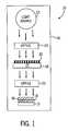
- FIG. 1is a general schematic block diagram of a lithographic system for patterning a wafer in accordance with an exemplary embodiment
- FIG. 2Ais a schematic top planar view of a first reticle or mask for use in the system illustrated in FIG. 1, the first reticle or mask includes alignment marks in accordance with another exemplary embodiment;
- FIG. 2Bis a schematic top planar view of a second reticle or mask for use in the system illustrated in FIG. 1, the second mask or reticle includes alignment marks in accordance with yet another exemplary embodiment;
- FIG. 3is a more detailed schematic top planar view of alignment marks for at least one of the first reticle or mask illustrated in FIG. 2 A and the second reticle or mask illustrated in FIG. 2B in accordance with still another exemplary embodiment;
- FIG. 4is a schematic top planar view of a wafer patterned by the system illustrated in FIG. 1 using the first mask or reticle illustrated in FIG. 2 A and the second mask or reticle illustrated in FIG. 2B, the wafer including wafer alignment marks indicating overlay errors in accordance with a further exemplary embodiment;
- FIG. 5is a schematic top planar view of a wafer patterned by the system illustrated in FIG. 1 using the first mask or reticle illustrated in FIG. 2 A and the second mask or reticle illustrated in FIG. 2B, the wafer including wafer alignment marks indicating small or no overlay errors in accordance with yet a further exemplary embodiment;
- FIG. 6is a schematic top planar view of a wafer patterned by the system illustrated in FIG. 1 using the first mask or reticle illustrated in FIG. 2 A and the second mask or reticle illustrated in FIG. 2B, the wafer including wafer alignment marks indicating overlay errors in accordance with another exemplary embodiment;
- FIG. 7is a schematic cross-sectional view of the wafer illustrated in FIG. 1, the wafer includes a photoresist material for patterning by the lithographic system illustrated in FIG. 1, in accordance with an exemplary embodiment;
- FIG. 8is a schematic cross-sectional view of the wafer illustrated in FIG. 7, the wafer patterned with the mask or reticle illustrated in FIG. 2 A by the lithographic system illustrated in FIG. 1, in accordance with yet another exemplary embodiment;
- FIG. 9is a schematic cross-sectional view of the wafer illustrated in FIG. 8, the wafer patterned with the mask or reticle illustrated in FIG. 2B by the lithographic system illustrated in FIG. 1, in accordance with still another exemplary embodiment;
- FIG. 10is a schematic cross-sectional view of the wafer illustrated in FIG. 9, the wafer developed to form wafer alignment marks, in accordance with a further exemplary embodiment.
- FIG. 11is a flow diagram showing a process for detecting overlay or alignment errors between masks or reticles, in accordance with yet another exemplary embodiment.
- Substrate 12can be a semiconductor substrate, such as, silicon, gallium arsenide, germanium, or other substrate material.
- Substrate 12can include one or more layers of material and/or features, such as, lines, interconnects, vias, doped portions, etc., and can further include devices, such as, transistors, microactuators, microsensors, capacitors, resistors, diodes, etc.
- Substrate 12can be an entire integrated circuit (IC) wafer or part of an IC wafer.
- Substrate 12can be part of an IC, such as, a memory, a processing unit, an input/output device, etc.
- Lithographic system 10provides a pattern of radiation to substrate 12 .
- System 10can include a chamber 50 .
- Chamber 50can be a vacuum or low pressure chamber for use in vacuum ultra-violet (VUV) lithography.
- Chamber 50can contain any of numerous types of atmospheres, such as, nitrogen, etc.
- lithographic system 10can be utilized in various other types of lithography including lithography that uses radiation at any number of wavelengths.
- Lithographic system 10includes a light source 22 , a condenser lens assembly 24 , a reticle or a mask 18 , and an objective lens assembly 26 .
- System 10can utilize a number of reticles or masks similar to reticle or mask 18 to fabricate various structures, layers and regions on substrate 12 .
- System 10can utilize reticles or masks 18 A and 18 B discussed below with reference to FIGS. 2A and 2B.
- a stagecan support substrate 12 and can move substrate 12 with respect to lens assembly 26 .
- System 10can have a variety of configurations and arrangements. The configuration of system 10 shown in FIG. 1 is exemplary.
- System 10can include mirrors, beam splitters, and other components arranged according to other designs.
- System 10can be embodied as a lithographic camera or stepper unit.
- An example of lithographic system 10is a PAS5500/xxx series machine manufactured by ASML.
- Other examplesinclude Microscan DUV systems by Silicon Valley Group or an XLS family Microlithography System by Integrated Solutions, Inc. of Korea.
- Substrate 12can include a layer of material 14 thereon.
- Layer of material 14can be an insulative layer, a conductive layer, a barrier layer, or other layer of material which is to be etched, doped, or layered using the process described herein.
- material 14is a hard mask layer, such as, a silicon nitride layer, a metal layer, or other material. The hard mask layer can serve as a patterned layer for processing of substrate 12 or for processing a layer upon substrate 12 .
- material 14is an anti-reflective coating (ARC).
- ARCanti-reflective coating
- Substrate 12 and layer of material 14are not described in a limiting fashion. The principles of the present invention can be applied to any integrated circuit substrate, wafer, mask layer, or other layer. Substrate 12 and the layer of material 14 can be conductive, semiconductive, or insulative.
- a layer of lithographic material, such as, a photoresist layer or material 16is deposited over layer of material 14 .
- Photoresist material 16can comprise any of a variety of photoresist chemicals suitable for lithographic applications.
- Material 16can be comprised of a matrix material or resin, a sensitizer or inhibitor, and a solvent.
- Photoresist material 16is preferably a lowcontrast photoresist, but may alternatively be a high-contrast photoresist.
- Photoresist material 16is deposited by, for example, spin-coating over layer of material 14 .
- Material 16can be provided with a thickness of less than 1.0 microns.
- Photoresist material 16may be either a positive photoresist or a negative photoresist and can be an organic or non-organic photoresist material.
- Reticle or mask 18is a binary mask in this exemplary embodiment.
- Reticle or mask 18has a translucent substrate 21 preferably fabricated from glass or quartz, and an opaque layer 20 , such as chromium or chromium oxide, patterned thereon.
- mask 18can be an attenuating phase shift mask, an alternating phase shift mask, or other mask reticle.
- Opaque layer 20is patterned to provide a desired circuit pattern to photoresist material 16 .
- the pattern associated with reticles or masks 18 A and 18 Bare described below in more detail. Although reticles or masks 18 , 18 A, 18 B are shown in a mask configuration and system 10 is shown using a mask configuration, the principles of the present invention are fully suited to reticle configurations.
- Light source 22provides light or radiation (e.g., ultraviolet (UV) light) through mask 18 to photoresist layer 16 .
- Light source 22is an excimer laser in this exemplary embodiment having a wavelength of 365 nanometers (nm), 248 nm, 193 nm, or 157 nm.
- light source 22may be any other light source having different wavelengths, including i-line deep ultra-violet (DUV), VUV, or extreme ultra-violet (EUV) wavelengths.
- DUVdeep ultra-violet
- EUVextreme ultra-violet
- reticles or masks 18 A or 18 Bcan be utilized in lithographic system 10 .
- Reticle or mask 18 A(FIG. 2A) includes an integrated circuit pattern 52 A
- reticle or mask 18 B(FIG. 2B) includes an integrated circuit pattern 52 B.
- Integrated circuit patterns 52 A and 52 Bare shown in an exemplary manner only. Patterns 52 A and 52 B are preferably provided in a center portion of reticles or masks 18 A and 18 B, respectively.
- reticles or masks 18 A and 18 Binclude alignment marks 54 .
- Alignment marks 54are essentially identical and are preferably provided in a peripheral region outside of patterns 52 A and 52 B. Marks 54 can be provided in the four corners associated with reticles or masks 18 A and 18 B.
- Marks 54preferably include a set of vertical bars 56 and a set of horizontal bars 58 . Bars 56 and 58 are generally so small that they cannot be seen with the human eye (e.g., without the aid of a lens or other optical device). Marks 54 are preferably patterned onto substrate 12 (e.g., layer 16 ) with system 10 as discussed below. Preferably, patterning occurs first with mask 18 A followed by mask 18 B so that marks 54 of reticle or mask 18 B are patterned over marks 54 of reticle or mask 18 A.
- mark 54is shown in more detail including vertical bars 56 and horizontal bars 58 .
- Vertical bars 56are configured to detect horizontal alignment errors
- horizontal bars 58are configured to detect rotational and vertical alignment errors.
- bars 56are located above bars 58 .
- bars 56 and 58can each have a width of 200 nm.
- the pitch or distance between individual barscan be 400 nm.
- the width to pitch ratiocan be one-to-one, one-to-two, or other ratio depending upon design considerations.
- Bars 56preferably have a length of 50 nm and bars 58 preferably have a length of 50 nm.
- Mark 54can include 125 bars 56 and 125 bars 58 .
- the specific structure of mark 54 with reference to FIG. 3is an exemplary embodiment only. Other patterns can be utilized to achieve the advantageous results in the present invention.
- a substrate 72can be utilized as substrate 12 in FIG. 1 .
- substrate 72has been subjected to a patterning process in system 10 during which integrated patterns 52 A and 52 B and alignment marks 54 associated with reticles or masks 18 A and 18 B have been provided to substrate 72 .
- the combination of integrated circuit patterns 52 A and 52 Bprovide a combine integrated circuit pattern 73 .
- Substrate 72also includes wafer alignment marks 74 , 75 , 76 and 77 .
- Wafer alignment marks 74 , 75 , 76 and 77a re associated with a combination of markings 54 of reticles or masks 18 A and 18 B.
- M arks 74 , 75 , 76 and 77have moire patterns which are viewable by the human eye. Therefore, although each line associated with marks 74 , 75 , 76 and 77 i s not visible by the human eye (e.g., because of their narrowness), marks 74 , 75 , 76 and 77 are visible to the human eye.
- marks 74 , 75 , 76 and 77indicate an alignment error to the naked eye.
- Mark 77is relatively darker than marks 74 , 75 and 76 .
- mark 76is lighter than marks 74 , 75 or 77 .
- the discrepancy in color between marks 74 , 75 , 76 and 77indicates an alignment error.
- mark 77is relatively dark, thereby indicating an alignment error.
- marks 74 , 75 , 76 and 77have different colors.
- the alignment errorcan be a vertical alignment error, a rotational alignment error, or a horizontal alignment error.
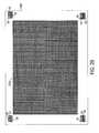
- a substrate 82is substantially similar to substrate 72 including combined IC pattern 73 and wafer alignment marks 84 , 85 , 86 and 87 .
- Marks 84 , 85 , 86 and 87are similar to marks 74 , 75 , 76 and 77 .
- marks 84 , 85 , 86 and 87have a similar color to each other and have a relatively light color, thereby indicating an absence or small level of alignment errors associated with reticles or masks 18 A and 18 B.
- a substrate 92is substantially similar to substrates 72 and 82 .
- Substrate 92includes combined integrated circuit pattern 73 and wafer alignment marks 94 , 95 , 96 and 97 .
- Wafer alignment marks 96 and 97are relatively dark, indicating the existence of an overlay error.
- wafer alignment marks 94 and 95are a substantially different level of darkness than marks 96 and 97 , also indicating the presence of an error.
- Marks 94 , 95 , 96 and 97are similar to alignment marks 74 , 75 , 76 and 77 (FIG. 4) and alignment marks 84 , 85 , 86 and 87 (FIG. 5 ).
- Substrate 12can be patterned in system 10 (FIG. 1) utilizing reticles or masks 18 A-B.
- the patterning of portion 111 including wafer alignment marks 174 (FIG. 10)is only discussed below for simplicity.
- Photoresist material 16is disposed above substrate 12 .
- Photoresist material 16can be applied by a spin coating machine, such as, an automated in-line wafer spin coater.
- substrate 12can be rotated to a speed of 2000-3000 rpm while photoresist material 16 is applied.
- photoresist material 16is a 0.1 to 1.0 micron thick layer.
- Substrate 12may be cleaned and primed before the application of material 16 .
- an anti-reflective coatingcan be provided above substrate 12 before material 16 is applied.
- light source 22provides an exposure of light or radiation through reticle or mask 18 A to selectively expose portion 111 of photoresist material 16 .
- the exposed sections 114 associated with alignment marks 54 (FIG. 2A) of reticle or mask 18 Aare formed in material 16 .
- Exposed sections 114can have a width of approximately 10 percent of the width of bars 56 (e.g., 10 nm) and are spaced approximately 10 percent of the distance between bars 56 (e.g., 20 nm).
- a predetermined amount of light energyis provided to photoresist material 16 in chamber 50 of system 10 .
- This predetermined amount of light energy provided to material 16is a factor of the intensity of light source 22 , the duration of the light provided, the wavelength of the light, the composition of photoresist material 16 , and any attenuation provided by mask 18 A.
- mJ/cm 2millijoules per square centimeter
- the intensity of light source 22the duration of the light provided
- the wavelength of the lightthe composition of photoresist material 16
- any attenuation provided by mask 18 Afor example, between 10 and 15 mJ/cm 2 can be applied in this first exposure step, using light source 22 having a 248 nm wavelength.
- a positive photoresist material 16is utilized, and sufficient light energy is provided through mask or reticle 18 A to chemically change material 16 to form sections 114 .
- light source 22provides an exposure of light or radiation through reticle or mask 18 B to selectively expose portion II of photoresist material 16 .
- Exposed sections 116 associated with alignment mark 54 (FIG. 2B) of reticle or mask 18 Bare formed in material 16 .
- Exposed sections 116can have a width of approximately 10 percent of the width of bars 56 (e.g., 10 nm) and are spaced approximately 10 percent of the distance between bars 56 (e.g., 20 nm).
- a predetermined amount of light energyis provided to photoresist material 16 in chamber 50 of system 10 .
- This predetermined amount of light energy provided to material 16is a factor of the intensity of light source 22 , the duration of the light provided, the wavelength of the light, the composition of photoresist material 16 , and any attenuation provided by mask 18 B.
- mJ/cm 2millijoules per square centimeter
- an emersion, puddling, or spray techniquecan be utilized to develop material 16 .
- an alignment error or overlay errorappears to exist, since sections 114 and 116 are not directly on top of each other. This alignment error will be manifested after material layer 16 has been developed.
- Any type of lithographic technologycan be used to pattern material 16 to form sections 114 and 116 .
- UV, DUV, VUV, or EUV lithographic equipmentcan be used to pattern photoresist material 16 .
- a developer solutionis provided to remove the portion associated with sections 114 and 116 .
- the developer solutionis typically a solvent which renders sections 114 and 116 soluble after being exposed to a sufficient amount of light energy.
- Sections 114 and 116can be associated with bars 56 of marks 54 of reticles or masks 18 A and 18 B, respectively.
- material 16includes trenches 118 associated with sections 114 and 116 . As can be seen, trenches 118 on a left side 122 will appear darker than trenches 118 on a right side 120 . This difference in coloration indicates an alignment error.
- an exemplary flow diagram 200is described.
- substrate 12 or a layer above substrate 12is covered by photoresist material 16 (FIG. 7 ).
- substrate 12is placed in a chamber and exposed to radiation via reticle or mask 18 A. The exposure of radiation provides photochemical reactions in material 16 (FIG. 8 ).
- substrate 12is exposed to radiation via reticle or mask 18 B.
- the exposure of radiationprovides additional photochemical reactions in material 16 (FIG. 9 ).
- material 16is developed in accordance with a conventional development process to form trenches 118 (FIG. 10) (wafer marks 74 , 75 , 76 and 77 (FIG. 4 ), wafer marks 84 , 85 , 86 , and 87 (FIG. 5 ), or wafer marks 94 , 95 , 96 , and 97 (FIG. 6 )).
- marks 74 , 75 , 76 , 77 or marks 84 , 85 , 86 , 87 , or marks 94 , 95 , 96 , 97are observed with the naked eye to determine if any overlay errors exist.
Landscapes
- Physics & Mathematics (AREA)
- General Physics & Mathematics (AREA)
- Exposure And Positioning Against Photoresist Photosensitive Materials (AREA)
Abstract
Description
Claims (20)
Priority Applications (1)
| Application Number | Priority Date | Filing Date | Title |
|---|---|---|---|
| US09/790,135US6489068B1 (en) | 2001-02-21 | 2001-02-21 | Process for observing overlay errors on lithographic masks |
Applications Claiming Priority (1)
| Application Number | Priority Date | Filing Date | Title |
|---|---|---|---|
| US09/790,135US6489068B1 (en) | 2001-02-21 | 2001-02-21 | Process for observing overlay errors on lithographic masks |
Publications (1)
| Publication Number | Publication Date |
|---|---|
| US6489068B1true US6489068B1 (en) | 2002-12-03 |
Family
ID=25149742
Family Applications (1)
| Application Number | Title | Priority Date | Filing Date |
|---|---|---|---|
| US09/790,135Expired - LifetimeUS6489068B1 (en) | 2001-02-21 | 2001-02-21 | Process for observing overlay errors on lithographic masks |
Country Status (1)
| Country | Link |
|---|---|
| US (1) | US6489068B1 (en) |
Cited By (52)
| Publication number | Priority date | Publication date | Assignee | Title |
|---|---|---|---|---|
| US20030206298A1 (en)* | 2002-05-02 | 2003-11-06 | Joerg Bischoff | Overlay measurements using zero-order cross polarization measurements |
| US20030212525A1 (en)* | 2002-01-31 | 2003-11-13 | Joerg Bischoff | Overlay measurements using periodic gratings |
| JP2004505439A (en)* | 2000-07-16 | 2004-02-19 | ボード・オブ・リージエンツ,ザ・ユニバーシテイ・オブ・テキサス・システム | High resolution overlay alignment method and system for transfer lithography |
| US20040112861A1 (en)* | 2002-12-11 | 2004-06-17 | Molecular Imprints, Inc. | Method for modulating shapes of substrates |
| US20040146792A1 (en)* | 2002-12-13 | 2004-07-29 | Molecular Imprints, Inc. | Magnification correction employing out-of-plane distortion of a substrate |
| US20040223131A1 (en)* | 2002-11-13 | 2004-11-11 | Molecular Imprints, Inc. | Chucking system for modulating shapes of substrates |
| US20050064676A1 (en)* | 2003-09-24 | 2005-03-24 | Renesas Technology Corp | Method of forming alignment mark |
| US6871558B2 (en) | 2002-12-12 | 2005-03-29 | Molecular Imprints, Inc. | Method for determining characteristics of substrate employing fluid geometries |
| US6873087B1 (en)* | 1999-10-29 | 2005-03-29 | Board Of Regents, The University Of Texas System | High precision orientation alignment and gap control stages for imprint lithography processes |
| US20050089773A1 (en)* | 2003-10-22 | 2005-04-28 | Applied Materials Israel Ltd. | System and method for measuring overlay errors |
| US6900881B2 (en) | 2002-07-11 | 2005-05-31 | Molecular Imprints, Inc. | Step and repeat imprint lithography systems |
| US6908861B2 (en) | 2002-07-11 | 2005-06-21 | Molecular Imprints, Inc. | Method for imprint lithography using an electric field |
| US6916584B2 (en) | 2002-08-01 | 2005-07-12 | Molecular Imprints, Inc. | Alignment methods for imprint lithography |
| US6926929B2 (en) | 2002-07-09 | 2005-08-09 | Molecular Imprints, Inc. | System and method for dispensing liquids |
| US6929762B2 (en) | 2002-11-13 | 2005-08-16 | Molecular Imprints, Inc. | Method of reducing pattern distortions during imprint lithography processes |
| US6932934B2 (en) | 2002-07-11 | 2005-08-23 | Molecular Imprints, Inc. | Formation of discontinuous films during an imprint lithography process |
| US20050219484A1 (en)* | 2004-04-06 | 2005-10-06 | Taiwan Semiconductor Manufacturing Co. | Novel method to simplify twin stage scanner OVL machine matching |
| US6954275B2 (en) | 2000-08-01 | 2005-10-11 | Boards Of Regents, The University Of Texas System | Methods for high-precision gap and orientation sensing between a transparent template and substrate for imprint lithography |
| US6964793B2 (en) | 2002-05-16 | 2005-11-15 | Board Of Regents, The University Of Texas System | Method for fabricating nanoscale patterns in light curable compositions using an electric field |
| US20050271955A1 (en)* | 2004-06-03 | 2005-12-08 | Board Of Regents, The University Of Texas System | System and method for improvement of alignment and overlay for microlithography |
| US20050270516A1 (en)* | 2004-06-03 | 2005-12-08 | Molecular Imprints, Inc. | System for magnification and distortion correction during nano-scale manufacturing |
| US20060019183A1 (en)* | 2004-07-20 | 2006-01-26 | Molecular Imprints, Inc. | Imprint alignment method, system, and template |
| US20060054814A1 (en)* | 2003-07-30 | 2006-03-16 | Dror Shemesh | Scanning electron microscope having multiple detectors and a method for multiple detector based imaging |
| US7027156B2 (en) | 2002-08-01 | 2006-04-11 | Molecular Imprints, Inc. | Scatterometry alignment for imprint lithography |
| US7037639B2 (en) | 2002-05-01 | 2006-05-02 | Molecular Imprints, Inc. | Methods of manufacturing a lithography template |
| US7060324B2 (en) | 2000-10-12 | 2006-06-13 | Board Of Regents, The University Of Texas System | Method of creating a dispersion of a liquid on a substrate |
| US20060132776A1 (en)* | 2004-12-21 | 2006-06-22 | Fujitsu Limited | Fabrication method of a semiconductor device |
| US7071088B2 (en) | 2002-08-23 | 2006-07-04 | Molecular Imprints, Inc. | Method for fabricating bulbous-shaped vias |
| US7070405B2 (en) | 2002-08-01 | 2006-07-04 | Molecular Imprints, Inc. | Alignment systems for imprint lithography |
| US7077992B2 (en) | 2002-07-11 | 2006-07-18 | Molecular Imprints, Inc. | Step and repeat imprint lithography processes |
| US7090716B2 (en) | 2003-10-02 | 2006-08-15 | Molecular Imprints, Inc. | Single phase fluid imprint lithography method |
| US7122079B2 (en) | 2004-02-27 | 2006-10-17 | Molecular Imprints, Inc. | Composition for an etching mask comprising a silicon-containing material |
| US7136150B2 (en) | 2003-09-25 | 2006-11-14 | Molecular Imprints, Inc. | Imprint lithography template having opaque alignment marks |
| US7150622B2 (en) | 2003-07-09 | 2006-12-19 | Molecular Imprints, Inc. | Systems for magnification and distortion correction for imprint lithography processes |
| US7157036B2 (en) | 2003-06-17 | 2007-01-02 | Molecular Imprints, Inc | Method to reduce adhesion between a conformable region and a pattern of a mold |
| US7179396B2 (en) | 2003-03-25 | 2007-02-20 | Molecular Imprints, Inc. | Positive tone bi-layer imprint lithography method |
| US20070231421A1 (en)* | 2006-04-03 | 2007-10-04 | Molecular Imprints, Inc. | Enhanced Multi Channel Alignment |
| US7292326B2 (en) | 2004-11-30 | 2007-11-06 | Molecular Imprints, Inc. | Interferometric analysis for the manufacture of nano-scale devices |
| US20070287081A1 (en)* | 2004-06-03 | 2007-12-13 | Molecular Imprints, Inc. | Method for obtaining force combinations for template deformation using nullspace and methods optimization techniques |
| US20080070481A1 (en)* | 2006-09-15 | 2008-03-20 | Nihon Micro Coating Co., Ltd. | Probe cleaner and cleaning method |
| US7396475B2 (en) | 2003-04-25 | 2008-07-08 | Molecular Imprints, Inc. | Method of forming stepped structures employing imprint lithography |
| US7452574B2 (en) | 2003-02-27 | 2008-11-18 | Molecular Imprints, Inc. | Method to reduce adhesion between a polymerizable layer and a substrate employing a fluorine-containing layer |
| US7630067B2 (en) | 2004-11-30 | 2009-12-08 | Molecular Imprints, Inc. | Interferometric analysis method for the manufacture of nano-scale devices |
| US7780893B2 (en) | 2006-04-03 | 2010-08-24 | Molecular Imprints, Inc. | Method of concurrently patterning a substrate having a plurality of fields and a plurality of alignment marks |
| US7906180B2 (en) | 2004-02-27 | 2011-03-15 | Molecular Imprints, Inc. | Composition for an etching mask comprising a silicon-containing material |
| US8016277B2 (en) | 2000-08-21 | 2011-09-13 | Board Of Regents, The University Of Texas System | Flexure based macro motion translation stage |
| US8076386B2 (en) | 2004-02-23 | 2011-12-13 | Molecular Imprints, Inc. | Materials for imprint lithography |
| US8211214B2 (en) | 2003-10-02 | 2012-07-03 | Molecular Imprints, Inc. | Single phase fluid imprint lithography method |
| US8349241B2 (en) | 2002-10-04 | 2013-01-08 | Molecular Imprints, Inc. | Method to arrange features on a substrate to replicate features having minimal dimensional variability |
| US20130017378A1 (en)* | 2009-05-29 | 2013-01-17 | Asml Netherlands B.V. | Apparatus and Method for Providing Resist Alignment Marks in a Double Patterning Lithographic Process |
| US9046475B2 (en) | 2011-05-19 | 2015-06-02 | Applied Materials Israel, Ltd. | High electron energy based overlay error measurement methods and systems |
| US9223202B2 (en) | 2000-07-17 | 2015-12-29 | Board Of Regents, The University Of Texas System | Method of automatic fluid dispensing for imprint lithography processes |
- 2001
- 2001-02-21USUS09/790,135patent/US6489068B1/ennot_activeExpired - Lifetime
Cited By (87)
| Publication number | Priority date | Publication date | Assignee | Title |
|---|---|---|---|---|
| US7098572B2 (en) | 1999-10-29 | 2006-08-29 | Board Of Regents, The University Of Texas System | Apparatus to control displacement of a body spaced-apart from a surface |
| US6955868B2 (en) | 1999-10-29 | 2005-10-18 | Board Of Regents, The University Of Texas System | Method to control the relative position between a body and a surface |
| US6873087B1 (en)* | 1999-10-29 | 2005-03-29 | Board Of Regents, The University Of Texas System | High precision orientation alignment and gap control stages for imprint lithography processes |
| US7060402B2 (en) | 1999-10-29 | 2006-06-13 | Board Of Regents, The University Of Texas System | Method of orientating a template with respect to a substrate in response to a force exerted on the template |
| JP2010087528A (en)* | 2000-07-16 | 2010-04-15 | Board Of Regents The Univ Of Texas System | Method of determining alignment between substrate, and template spaced apart from the substrate at predetermined distance |
| JP2010087526A (en)* | 2000-07-16 | 2010-04-15 | Board Of Regents The Univ Of Texas System | Imprint lithography system having template, and method of aligning substrate and template |
| US20040189994A1 (en)* | 2000-07-16 | 2004-09-30 | Board Of Regents, The University Of Texas System | Method of determining alignment of a template and a substrate having a liquid disposed therebetween |
| JP2010087529A (en)* | 2000-07-16 | 2010-04-15 | Board Of Regents The Univ Of Texas System | Template, and imprint lithography system |
| US7303383B1 (en) | 2000-07-16 | 2007-12-04 | Board Of Regents, The University Of Texas System | Imprint lithography system to produce light to impinge upon and polymerize a liquid in superimposition with template overlay marks |
| US6842229B2 (en) | 2000-07-16 | 2005-01-11 | Board Of Regents, The University Of Texas System | Imprint lithography template comprising alignment marks |
| US7186483B2 (en) | 2000-07-16 | 2007-03-06 | Board Of Regents, The University Of Texas System | Method of determining alignment of a template and a substrate having a liquid disposed therebetween |
| US6919152B2 (en) | 2000-07-16 | 2005-07-19 | Board Of Regents, The University Of Texas System | High resolution overlay alignment systems for imprint lithography |
| US6921615B2 (en) | 2000-07-16 | 2005-07-26 | Board Of Regents, The University Of Texas System | High-resolution overlay alignment methods for imprint lithography |
| JP2004505439A (en)* | 2000-07-16 | 2004-02-19 | ボード・オブ・リージエンツ,ザ・ユニバーシテイ・オブ・テキサス・システム | High resolution overlay alignment method and system for transfer lithography |
| US6986975B2 (en)* | 2000-07-16 | 2006-01-17 | Board Of Regents, The University Of Texas System | Method of aligning a template with a substrate employing moire patterns |
| US6916585B2 (en) | 2000-07-16 | 2005-07-12 | Board Of Regents, The University Of Texas Systems | Method of varying template dimensions to achieve alignment during imprint lithography |
| US6902853B2 (en) | 2000-07-16 | 2005-06-07 | Board Of Regents, The University Of Texas System | Dual wavelength method of determining a relative position of a substrate and a template |
| US9223202B2 (en) | 2000-07-17 | 2015-12-29 | Board Of Regents, The University Of Texas System | Method of automatic fluid dispensing for imprint lithography processes |
| US6954275B2 (en) | 2000-08-01 | 2005-10-11 | Boards Of Regents, The University Of Texas System | Methods for high-precision gap and orientation sensing between a transparent template and substrate for imprint lithography |
| US8016277B2 (en) | 2000-08-21 | 2011-09-13 | Board Of Regents, The University Of Texas System | Flexure based macro motion translation stage |
| US7060324B2 (en) | 2000-10-12 | 2006-06-13 | Board Of Regents, The University Of Texas System | Method of creating a dispersion of a liquid on a substrate |
| US6772084B2 (en) | 2002-01-31 | 2004-08-03 | Timbre Technologies, Inc. | Overlay measurements using periodic gratings |
| US20030212525A1 (en)* | 2002-01-31 | 2003-11-13 | Joerg Bischoff | Overlay measurements using periodic gratings |
| US7037639B2 (en) | 2002-05-01 | 2006-05-02 | Molecular Imprints, Inc. | Methods of manufacturing a lithography template |
| US20050030536A1 (en)* | 2002-05-02 | 2005-02-10 | Timbre Technologies, Inc. | Overlay measurements using zero-order cross polarization measurements |
| US20030206298A1 (en)* | 2002-05-02 | 2003-11-06 | Joerg Bischoff | Overlay measurements using zero-order cross polarization measurements |
| US6947141B2 (en)* | 2002-05-02 | 2005-09-20 | Timbre Technologies, Inc. | Overlay measurements using zero-order cross polarization measurements |
| US6804005B2 (en)* | 2002-05-02 | 2004-10-12 | Timbre Technologies, Inc. | Overlay measurements using zero-order cross polarization measurements |
| US6964793B2 (en) | 2002-05-16 | 2005-11-15 | Board Of Regents, The University Of Texas System | Method for fabricating nanoscale patterns in light curable compositions using an electric field |
| US6926929B2 (en) | 2002-07-09 | 2005-08-09 | Molecular Imprints, Inc. | System and method for dispensing liquids |
| US6900881B2 (en) | 2002-07-11 | 2005-05-31 | Molecular Imprints, Inc. | Step and repeat imprint lithography systems |
| US7077992B2 (en) | 2002-07-11 | 2006-07-18 | Molecular Imprints, Inc. | Step and repeat imprint lithography processes |
| US6932934B2 (en) | 2002-07-11 | 2005-08-23 | Molecular Imprints, Inc. | Formation of discontinuous films during an imprint lithography process |
| US6908861B2 (en) | 2002-07-11 | 2005-06-21 | Molecular Imprints, Inc. | Method for imprint lithography using an electric field |
| US7027156B2 (en) | 2002-08-01 | 2006-04-11 | Molecular Imprints, Inc. | Scatterometry alignment for imprint lithography |
| US7070405B2 (en) | 2002-08-01 | 2006-07-04 | Molecular Imprints, Inc. | Alignment systems for imprint lithography |
| US6916584B2 (en) | 2002-08-01 | 2005-07-12 | Molecular Imprints, Inc. | Alignment methods for imprint lithography |
| US7071088B2 (en) | 2002-08-23 | 2006-07-04 | Molecular Imprints, Inc. | Method for fabricating bulbous-shaped vias |
| US8349241B2 (en) | 2002-10-04 | 2013-01-08 | Molecular Imprints, Inc. | Method to arrange features on a substrate to replicate features having minimal dimensional variability |
| US7019819B2 (en) | 2002-11-13 | 2006-03-28 | Molecular Imprints, Inc. | Chucking system for modulating shapes of substrates |
| US6982783B2 (en) | 2002-11-13 | 2006-01-03 | Molecular Imprints, Inc. | Chucking system for modulating shapes of substrates |
| US20040223131A1 (en)* | 2002-11-13 | 2004-11-11 | Molecular Imprints, Inc. | Chucking system for modulating shapes of substrates |
| US6929762B2 (en) | 2002-11-13 | 2005-08-16 | Molecular Imprints, Inc. | Method of reducing pattern distortions during imprint lithography processes |
| US20040112861A1 (en)* | 2002-12-11 | 2004-06-17 | Molecular Imprints, Inc. | Method for modulating shapes of substrates |
| US6980282B2 (en) | 2002-12-11 | 2005-12-27 | Molecular Imprints, Inc. | Method for modulating shapes of substrates |
| US6871558B2 (en) | 2002-12-12 | 2005-03-29 | Molecular Imprints, Inc. | Method for determining characteristics of substrate employing fluid geometries |
| US7323130B2 (en) | 2002-12-13 | 2008-01-29 | Molecular Imprints, Inc. | Magnification correction employing out-of-plane distortion of a substrate |
| US20040146792A1 (en)* | 2002-12-13 | 2004-07-29 | Molecular Imprints, Inc. | Magnification correction employing out-of-plane distortion of a substrate |
| US7452574B2 (en) | 2003-02-27 | 2008-11-18 | Molecular Imprints, Inc. | Method to reduce adhesion between a polymerizable layer and a substrate employing a fluorine-containing layer |
| US7179396B2 (en) | 2003-03-25 | 2007-02-20 | Molecular Imprints, Inc. | Positive tone bi-layer imprint lithography method |
| US7396475B2 (en) | 2003-04-25 | 2008-07-08 | Molecular Imprints, Inc. | Method of forming stepped structures employing imprint lithography |
| US7157036B2 (en) | 2003-06-17 | 2007-01-02 | Molecular Imprints, Inc | Method to reduce adhesion between a conformable region and a pattern of a mold |
| US7150622B2 (en) | 2003-07-09 | 2006-12-19 | Molecular Imprints, Inc. | Systems for magnification and distortion correction for imprint lithography processes |
| US20060054814A1 (en)* | 2003-07-30 | 2006-03-16 | Dror Shemesh | Scanning electron microscope having multiple detectors and a method for multiple detector based imaging |
| US7847267B2 (en) | 2003-07-30 | 2010-12-07 | Applied Materials Israel, Ltd. | Scanning electron microscope having multiple detectors and a method for multiple detector based imaging |
| US20050064676A1 (en)* | 2003-09-24 | 2005-03-24 | Renesas Technology Corp | Method of forming alignment mark |
| US7136150B2 (en) | 2003-09-25 | 2006-11-14 | Molecular Imprints, Inc. | Imprint lithography template having opaque alignment marks |
| US7090716B2 (en) | 2003-10-02 | 2006-08-15 | Molecular Imprints, Inc. | Single phase fluid imprint lithography method |
| US8211214B2 (en) | 2003-10-02 | 2012-07-03 | Molecular Imprints, Inc. | Single phase fluid imprint lithography method |
| US20050089773A1 (en)* | 2003-10-22 | 2005-04-28 | Applied Materials Israel Ltd. | System and method for measuring overlay errors |
| US7842933B2 (en) | 2003-10-22 | 2010-11-30 | Applied Materials Israel, Ltd. | System and method for measuring overlay errors |
| US8076386B2 (en) | 2004-02-23 | 2011-12-13 | Molecular Imprints, Inc. | Materials for imprint lithography |
| US7906180B2 (en) | 2004-02-27 | 2011-03-15 | Molecular Imprints, Inc. | Composition for an etching mask comprising a silicon-containing material |
| US7122079B2 (en) | 2004-02-27 | 2006-10-17 | Molecular Imprints, Inc. | Composition for an etching mask comprising a silicon-containing material |
| US20050219484A1 (en)* | 2004-04-06 | 2005-10-06 | Taiwan Semiconductor Manufacturing Co. | Novel method to simplify twin stage scanner OVL machine matching |
| US7333173B2 (en)* | 2004-04-06 | 2008-02-19 | Taiwan Semiconductor Manufacturing Company | Method to simplify twin stage scanner OVL machine matching |
| US20050270516A1 (en)* | 2004-06-03 | 2005-12-08 | Molecular Imprints, Inc. | System for magnification and distortion correction during nano-scale manufacturing |
| US7535549B2 (en) | 2004-06-03 | 2009-05-19 | Board Of Regents, University Of Texas System | System and method for improvement of alignment and overlay for microlithography |
| US20070287081A1 (en)* | 2004-06-03 | 2007-12-13 | Molecular Imprints, Inc. | Method for obtaining force combinations for template deformation using nullspace and methods optimization techniques |
| US7298456B2 (en) | 2004-06-03 | 2007-11-20 | Molecular Imprints, Inc. | System for varying dimensions of a substrate during nanoscale manufacturing |
| US20060001194A1 (en)* | 2004-06-03 | 2006-01-05 | Molecular Imprints, Inc. | System for varying dimensions of a substrate during nanoscale manufacturing |
| US7768624B2 (en) | 2004-06-03 | 2010-08-03 | Board Of Regents, The University Of Texas System | Method for obtaining force combinations for template deformation using nullspace and methods optimization techniques |
| US20050271955A1 (en)* | 2004-06-03 | 2005-12-08 | Board Of Regents, The University Of Texas System | System and method for improvement of alignment and overlay for microlithography |
| US20060019183A1 (en)* | 2004-07-20 | 2006-01-26 | Molecular Imprints, Inc. | Imprint alignment method, system, and template |
| US7785526B2 (en) | 2004-07-20 | 2010-08-31 | Molecular Imprints, Inc. | Imprint alignment method, system, and template |
| US8366434B2 (en)* | 2004-07-20 | 2013-02-05 | Molecular Imprints, Inc. | Imprint alignment method, system and template |
| US7785096B2 (en) | 2004-11-30 | 2010-08-31 | Molecular Imprints, Inc. | Enhanced multi channel alignment |
| US7880872B2 (en) | 2004-11-30 | 2011-02-01 | Molecular Imprints, Inc. | Interferometric analysis method for the manufacture of nano-scale devices |
| US7630067B2 (en) | 2004-11-30 | 2009-12-08 | Molecular Imprints, Inc. | Interferometric analysis method for the manufacture of nano-scale devices |
| US7292326B2 (en) | 2004-11-30 | 2007-11-06 | Molecular Imprints, Inc. | Interferometric analysis for the manufacture of nano-scale devices |
| US20060132776A1 (en)* | 2004-12-21 | 2006-06-22 | Fujitsu Limited | Fabrication method of a semiconductor device |
| US7270920B2 (en)* | 2004-12-21 | 2007-09-18 | Fujitsu Limited | Fabrication method of a semiconductor device |
| US20070231421A1 (en)* | 2006-04-03 | 2007-10-04 | Molecular Imprints, Inc. | Enhanced Multi Channel Alignment |
| US7780893B2 (en) | 2006-04-03 | 2010-08-24 | Molecular Imprints, Inc. | Method of concurrently patterning a substrate having a plurality of fields and a plurality of alignment marks |
| US20080070481A1 (en)* | 2006-09-15 | 2008-03-20 | Nihon Micro Coating Co., Ltd. | Probe cleaner and cleaning method |
| US20130017378A1 (en)* | 2009-05-29 | 2013-01-17 | Asml Netherlands B.V. | Apparatus and Method for Providing Resist Alignment Marks in a Double Patterning Lithographic Process |
| US9046475B2 (en) | 2011-05-19 | 2015-06-02 | Applied Materials Israel, Ltd. | High electron energy based overlay error measurement methods and systems |
Similar Documents
| Publication | Publication Date | Title |
|---|---|---|
| US6489068B1 (en) | Process for observing overlay errors on lithographic masks | |
| US7981595B2 (en) | Reduced pitch multiple exposure process | |
| US5439764A (en) | Mask having multiple patterns | |
| CN101963756A (en) | Form the method for electron device | |
| US8394574B2 (en) | Metrology systems and methods for lithography processes | |
| US7794921B2 (en) | Imaging post structures using x and y dipole optics and a single mask | |
| US7906270B2 (en) | Reduced pitch multiple exposure process | |
| US6764808B2 (en) | Self-aligned pattern formation using wavelenghts | |
| US20090170024A1 (en) | Method of Patterning a Substrate, Photosensitive Layer Stack and System for Lithography | |
| US20090219496A1 (en) | Methods of Double Patterning, Photo Sensitive Layer Stack for Double Patterning and System for Double Patterning | |
| US6902851B1 (en) | Method for using phase-shifting mask | |
| US6602794B1 (en) | Silylation process for forming contacts | |
| JP2002075857A (en) | Method of forming resist pattern | |
| US20050208427A1 (en) | Semiconductor device manufacturing method | |
| US8257911B2 (en) | Method of process optimization for dual tone development | |
| US6555274B1 (en) | Pupil filtering for a lithographic tool | |
| US7642021B2 (en) | Method of mapping lithography focus errors | |
| JP2000267257A (en) | Mask and exposure method using the same | |
| EP1288721B1 (en) | Photolithography with multiple level substrate | |
| US6555234B1 (en) | Barrier for and a method of reducing outgassing from a photoresist material | |
| US20050277065A1 (en) | Method of manufacturing a semiconductor device | |
| US20100055624A1 (en) | Method of patterning a substrate using dual tone development | |
| US6784070B2 (en) | Intra-cell mask alignment for improved overlay | |
| US6548384B2 (en) | Method for performing lithographic process to a multi-layered photoresist layer | |
| US20070015088A1 (en) | Method for lithographically printing tightly nested and isolated hole features using double exposure |
Legal Events
| Date | Code | Title | Description |
|---|---|---|---|
| AS | Assignment | Owner name:ADVANCED MICRO DEVICES, INC., CALIFORNIA Free format text:ASSIGNMENT OF ASSIGNORS INTEREST;ASSIGNOR:KYE, JONGWOOK;REEL/FRAME:011564/0612 Effective date:20010216 | |
| STCF | Information on status: patent grant | Free format text:PATENTED CASE | |
| CC | Certificate of correction | ||
| FEPP | Fee payment procedure | Free format text:PAYOR NUMBER ASSIGNED (ORIGINAL EVENT CODE: ASPN); ENTITY STATUS OF PATENT OWNER: LARGE ENTITY | |
| FPAY | Fee payment | Year of fee payment:4 | |
| AS | Assignment | Owner name:GLOBALFOUNDRIES INC., CAYMAN ISLANDS Free format text:AFFIRMATION OF PATENT ASSIGNMENT;ASSIGNOR:ADVANCED MICRO DEVICES, INC.;REEL/FRAME:023119/0083 Effective date:20090630 | |
| FPAY | Fee payment | Year of fee payment:8 | |
| FPAY | Fee payment | Year of fee payment:12 | |
| AS | Assignment | Owner name:WILMINGTON TRUST, NATIONAL ASSOCIATION, DELAWARE Free format text:SECURITY AGREEMENT;ASSIGNOR:GLOBALFOUNDRIES INC.;REEL/FRAME:049490/0001 Effective date:20181127 | |
| AS | Assignment | Owner name:GLOBALFOUNDRIES INC., CAYMAN ISLANDS Free format text:RELEASE BY SECURED PARTY;ASSIGNOR:WILMINGTON TRUST, NATIONAL ASSOCIATION;REEL/FRAME:054636/0001 Effective date:20201117 | |
| AS | Assignment | Owner name:GLOBALFOUNDRIES U.S. INC., NEW YORK Free format text:RELEASE BY SECURED PARTY;ASSIGNOR:WILMINGTON TRUST, NATIONAL ASSOCIATION;REEL/FRAME:056987/0001 Effective date:20201117 |