US6488984B1 - Film deposition method and apparatus - Google Patents
Film deposition method and apparatusDownload PDFInfo
- Publication number
- US6488984B1 US6488984B1US09/830,633US83063301AUS6488984B1US 6488984 B1US6488984 B1US 6488984B1US 83063301 AUS83063301 AUS 83063301AUS 6488984 B1US6488984 B1US 6488984B1
- Authority
- US
- United States
- Prior art keywords
- metal layer
- film deposition
- processed body
- barrier metal
- fluid
- Prior art date
- Legal status (The legal status is an assumption and is not a legal conclusion. Google has not performed a legal analysis and makes no representation as to the accuracy of the status listed.)
- Expired - Fee Related
Links
Images


Classifications
- H—ELECTRICITY
- H01—ELECTRIC ELEMENTS
- H01L—SEMICONDUCTOR DEVICES NOT COVERED BY CLASS H10
- H01L21/00—Processes or apparatus adapted for the manufacture or treatment of semiconductor or solid state devices or of parts thereof
- H01L21/70—Manufacture or treatment of devices consisting of a plurality of solid state components formed in or on a common substrate or of parts thereof; Manufacture of integrated circuit devices or of parts thereof
- H01L21/71—Manufacture of specific parts of devices defined in group H01L21/70
- H01L21/768—Applying interconnections to be used for carrying current between separate components within a device comprising conductors and dielectrics
- H01L21/76838—Applying interconnections to be used for carrying current between separate components within a device comprising conductors and dielectrics characterised by the formation and the after-treatment of the conductors
- H01L21/76877—Filling of holes, grooves or trenches, e.g. vias, with conductive material
- C—CHEMISTRY; METALLURGY
- C23—COATING METALLIC MATERIAL; COATING MATERIAL WITH METALLIC MATERIAL; CHEMICAL SURFACE TREATMENT; DIFFUSION TREATMENT OF METALLIC MATERIAL; COATING BY VACUUM EVAPORATION, BY SPUTTERING, BY ION IMPLANTATION OR BY CHEMICAL VAPOUR DEPOSITION, IN GENERAL; INHIBITING CORROSION OF METALLIC MATERIAL OR INCRUSTATION IN GENERAL
- C23C—COATING METALLIC MATERIAL; COATING MATERIAL WITH METALLIC MATERIAL; SURFACE TREATMENT OF METALLIC MATERIAL BY DIFFUSION INTO THE SURFACE, BY CHEMICAL CONVERSION OR SUBSTITUTION; COATING BY VACUUM EVAPORATION, BY SPUTTERING, BY ION IMPLANTATION OR BY CHEMICAL VAPOUR DEPOSITION, IN GENERAL
- C23C18/00—Chemical coating by decomposition of either liquid compounds or solutions of the coating forming compounds, without leaving reaction products of surface material in the coating; Contact plating
- C23C18/02—Chemical coating by decomposition of either liquid compounds or solutions of the coating forming compounds, without leaving reaction products of surface material in the coating; Contact plating by thermal decomposition
- C23C18/08—Chemical coating by decomposition of either liquid compounds or solutions of the coating forming compounds, without leaving reaction products of surface material in the coating; Contact plating by thermal decomposition characterised by the deposition of metallic material
- H—ELECTRICITY
- H01—ELECTRIC ELEMENTS
- H01L—SEMICONDUCTOR DEVICES NOT COVERED BY CLASS H10
- H01L21/00—Processes or apparatus adapted for the manufacture or treatment of semiconductor or solid state devices or of parts thereof
- H01L21/02—Manufacture or treatment of semiconductor devices or of parts thereof
- H01L21/04—Manufacture or treatment of semiconductor devices or of parts thereof the devices having potential barriers, e.g. a PN junction, depletion layer or carrier concentration layer
- H01L21/18—Manufacture or treatment of semiconductor devices or of parts thereof the devices having potential barriers, e.g. a PN junction, depletion layer or carrier concentration layer the devices having semiconductor bodies comprising elements of Group IV of the Periodic Table or AIIIBV compounds with or without impurities, e.g. doping materials
- H01L21/28—Manufacture of electrodes on semiconductor bodies using processes or apparatus not provided for in groups H01L21/20 - H01L21/268
- H01L21/283—Deposition of conductive or insulating materials for electrodes conducting electric current
- H01L21/285—Deposition of conductive or insulating materials for electrodes conducting electric current from a gas or vapour, e.g. condensation
- H01L21/28506—Deposition of conductive or insulating materials for electrodes conducting electric current from a gas or vapour, e.g. condensation of conductive layers
- H01L21/28512—Deposition of conductive or insulating materials for electrodes conducting electric current from a gas or vapour, e.g. condensation of conductive layers on semiconductor bodies comprising elements of Group IV of the Periodic Table
- H01L21/28556—Deposition of conductive or insulating materials for electrodes conducting electric current from a gas or vapour, e.g. condensation of conductive layers on semiconductor bodies comprising elements of Group IV of the Periodic Table by chemical means, e.g. CVD, LPCVD, PECVD, laser CVD
- H—ELECTRICITY
- H01—ELECTRIC ELEMENTS
- H01L—SEMICONDUCTOR DEVICES NOT COVERED BY CLASS H10
- H01L21/00—Processes or apparatus adapted for the manufacture or treatment of semiconductor or solid state devices or of parts thereof
- H01L21/67—Apparatus specially adapted for handling semiconductor or electric solid state devices during manufacture or treatment thereof; Apparatus specially adapted for handling wafers during manufacture or treatment of semiconductor or electric solid state devices or components ; Apparatus not specifically provided for elsewhere
- H01L21/67005—Apparatus not specifically provided for elsewhere
- H01L21/67011—Apparatus for manufacture or treatment
- H01L21/6715—Apparatus for applying a liquid, a resin, an ink or the like
Definitions
- the present inventionrelates to the process of manufacturing a semiconductor device.
- itrelates to techniques of forming a metal film onto a to-be-processed body such as a semiconductor wafer.
- MOCVDmetalorganic chemical vapor deposition
- Processes that are also given considerationinvolve applying the organic metal as it is or mixed with an organic solvent (an organometallic fluid) onto the wafer while heating the wafer that has been placed in the process chamber, and then causing a pyrolytic decomposition reaction to occur in order to form the metallic film.
- organic solventan organometallic fluid
- a barrier metal layersuch as tantalum or tantalum nitride has conventionally been formed before depositing the metal film.
- the object of the present inventionis to provide a method of film deposition, and an apparatus thereof, that can perform film deposition of a metallic film without having the problems described above.
- the inventorsconsidered many variables. As a result, they concluded that the barrier metal layer might be affected by factors such as natural evaporation since the wafer is conventionally exposed to air after the barrier metal layer is formed.
- the present inventionis a film deposition method that forms a metal layer after forming a barrier metal layer on a to-be-processed body; wherein one series of processing from formation of the barrier metal up to and including formation of the metal layer is performed in an environment cut off from air.
- the performing of the barrier metal layer formation in a first device and the metal layer formation in a second device; and the transport of a to-be-processed body from the first device to the second deviceis performed through a transport pathway that is cut off from air.
- the metal layer formationcomprise a first step of preparing an organometallic fluid, which contains an organic metal such as (hfac)Cu +1 (tmvs) as its main component and which precipitates a metal layer material through a pyrolytic decomposition reaction, and then applying the organometallic fluid onto the to-be-processed body at a temperature within the non-reactive range of the organic metal; and a second step of heating the to-be-processed body to a predetermined temperature after the first step, and causing a pyrolytic decomposition reaction of the organic metal within the fluid that is applied to the to-be-processed body.
- an organometallic fluidwhich contains an organic metal such as (hfac)Cu +1 (tmvs) as its main component and which precipitates a metal layer material through a pyrolytic decomposition reaction
- barrier metal layerafter formation of barrier metal layer, a thin film of the same metal material as that of the metal layer be formed on the barrier metal layer as a seed layer.
- the film deposition apparatusthat embodies the film deposition method of the present invention is most effective when it comprises a first device, which forms a barrier metal layer in an environment that is cut off from air; a second device, which forms a metal layer in an environment that is cut off from air; and a transport pathway, which connects the first device and the second device, and is cut off from air.
- this film deposition apparatusfurther comprise a third device that forms a thin layer made of the same metal material as that of the metal layer, as a seed layer in an environment cut off from air.
- FIGS. 1 a to 1 care partial cross-sectional views showing the state of the semiconductor wafer as diagrams that schematically illustrate steps of the film deposition method according to the present invention
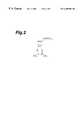
- FIG. 2illustrates the constitutional formula of (hfac)Cu +1 (tmvs);
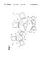
- FIG. 3is an abbreviated explanatory diagram showing the first embodiment of the film deposition apparatus according to the present invention.
- FIG. 4is a schematic diagram showing the process chamber used for application in the copper film deposition apparatus of FIG. 3;
- FIG. 5is a schematic diagram showing the process chamber used for pyrolytic decomposition in the copper film deposition apparatus of FIG. 3;
- FIG. 6illustrates the pyrolytic decomposition reaction of (hfac)Cu +1 (tmvs).
- thin film 3as a barrier metal layer from a material such as tantalum (Ta), tantalum nitride (TaN), titanium nitride (TiN) or tungsten nitride (WN), on the semiconductor wafer (to-be-processed body) W that has insulating layer 2 , such as a silicon oxide film (SiO 2 ), formed on copper interconnect layer 1 , then depositing copper thin film 5 is assumed, with the organic metal (hfac)Cu +1 (tmvs) assumed to be the base material of copper layer 5 .
- a materialsuch as tantalum (Ta), tantalum nitride (TaN), titanium nitride (TiN) or tungsten nitride (WN)
- the constitutional formula of (hfac)Cu +1 (tmvs)is shown in FIG. 2, and is in its liquid state at room temperature and under normal pressure. Since the viscosity of (hfac)Cu +l (tmvs) is low, it may be applicable for use as it is in film deposition method of the present invention; however, in the following embodiments, it is mixed with the organic solvent heptadecane for greater ease in handling.
- process fluidthe fluid that contains this (hfac)Cu +1 (tmvs) is referred to as “process fluid”.
- FIG. 3is a schematic diagram showing the first embodiment of film deposition apparatus 10 according to the present invention.
- This film deposition apparatus 10is multi-chambered, and comprises first transfer chamber (transport pathway) 12 , which maintains a predetermined degree of vacuum inside; and first process chamber 14 and second processing 16 , which are configured around the periphery of first transfer chamber 12 .
- First process chamber 14has structured a sputtering device (first device) for forming the barrier metal layer
- second process chamber 16has structured a sputtering device (third device) for forming a seed layer.
- Load lock chambers 18 and 20are also connected around the periphery of first transfer chamber 12 , and these load lock chambers 18 and 20 are configured in a manner such that cassette holders 22 and 24 , which hold a plurality of wafers W, may be installed from the outside.
- copper film deposition device (second device) 26which performs film deposition by applying the process fluid onto wafer W and then causing a pyrolytic decomposition reaction of the organic material within the process fluid to occur in order to deposit the copper film, is connected to first transfer chamber 12 via the small capacity buffer chamber 28 .
- Transport robot 30is provided in first transfer chamber 12 , and each of the chambers 12 , 14 , 16 , 18 , 20 and 28 are configured such that wafer W may be transferred between them without being exposed to air.
- Copper film deposition device 26comprises third process chamber 32 , which performs the process of applying process fluid onto wafer W; fourth process chamber 34 , which performs the process of pyrolytically decomposing the organic metal, namely (hfac)Cu +1 (tmvs); and second transfer chamber 36 , which is configured between both of chambers 34 and 32 . Within second transfer chamber 36 , there is also provided transport robot 38 , making it feasible for wafer W to be transferred among chambers 28 , 32 , 34 , and 36 .
- reference numerals 40 to 47denote slit valves that open and close the wafer transport pathways between the chambers.
- the first process chamber 14comprises a film deposition device, for example a sputtering device not specifically shown in the Figures, which is a conventionally well known device that uses a target material for the barrier metal layer, for example tantalum.
- second process chamber 16also comprises a film deposition device, for example a sputtering device that is also not specifically shown in the Figures, which is a conventionally well known device that uses copper as a target material.
- turntable 50is configured within third process chamber in copper film deposition device 26 to support wafer W.
- Wafer Wis placed horizontally on this turntable 50 and held in place using an appropriate fixing means such as a vacuum chuck, which is not shown in the Figure.
- the diameter of turntable 50is shown in the Figure smaller than the diameter of wafer W; however, when the diameter of turntable 50 is larger than that of wafer W, not only does the process fluid adhere to wafer W, but also to the exposed portions of turntable 50 , which can have negative repercussions for the next wafer W to be processed.
- Turntable 50further comprises drive motor 52 , which is configured external to third process chamber 32 in a manner that allows it to rotate turntable 50 at relatively high speeds.
- Application device 54is provided in order to apply process fluid to the surface of wafer W.
- Application device 54comprises supply pipeline 58 , which introduces process fluid from process fluid supply system (supply means) 56 , which is configured external to third process chamber 32 ; and nozzle 60 , which extends horizontally from the upper end of supply pipeline 58 and its end facing downward.
- Supply pipeline 58is configured so that it may be rotationally driven both backwards and forwards by actuator 62 , which may be, for example, a drive motor, and because of this nozzle 60 is able to swing about the center axis of supply pipeline 58 .
- nozzle 60Since the distance from the axis of supply pipeline 58 to the end of nozzle 60 is approximately the same as the distance from the axis of supply pipeline 58 to the rotational center of turntable 50 , and as a result of this, nozzle 60 is able to pass above the exact center of wafer W supported on turntable 50 .
- turntable 64is configured inside fourth process chamber 34 in order to hold wafer W in a manner such that it can be rotated.
- This turntable 64has basically the same mechanism as turntable 50 in third process chamber 32 , whereby it is rotated by drive motor 66 and can hold wafer W in place using an applicable means such as a vacuum chuck.
- turn table 64rotates at a slower speed than turntable 50 in first process chamber 32 .
- the diameter of turntable 64is made larger than the diameter of wafer W.
- a plurality of heating lamps 68which may be for example halogen lamps, are configured to be placed behind silica glass plate 70 .
- This configurationallows the surface of the wafer W that is locked onto turntable 64 to be heated.
- Temperature controlis achieved based on the signals output from temperature gages such as a thermoelectric couple attached to turntable 64 or a pyrometer configured on the ceiling of process chamber 34 , and is performed by turning heating lamps 68 on and off, or regulating the amount of power input to them.
- a supply source of an inert gas such as a nitrogen gasis connected to each of third process chamber 32 , fourth process chamber 34 , second transfer chamber 36 , and buffer chamber 28 , respectively, so that the air inside each chamber may be changed into an inert gas atmosphere.
- each of the respective chambers inside film deposition apparatus 10is connected to a vacuum pump. The driving of each chamber, the gas supply, and the driving of the transport robot all fall under the management of a control device not shown in the Figures.
- Processingis performed in the following order when forming the layers as shown in FIG. 1 c using this type of multi-chambered film deposition apparatus 10 , according to the present invention.
- a cassette holder 22which contains wafers W on which have been formed a predetermined pattern of insulating film 2 on the copper interconnect layer 1 , is set into load lock chamber 18 , an empty cassette holder 24 is set inside the other load lock chamber 20 .
- the vacuum pump connected to each of the chambersis activated, and the pressure inside each chamber is adjusted.
- each of the chambers 32 , 34 , and 36 inside copper film deposition device 26are made to have an inert gas environment at the normal atmospheric pressure level.
- Slit valve 40is then opened, one wafer W is taken out of cassette holder 18 using transport robot 30 , and it is transferred to first transfer chamber 12 .
- slit valve 40is closed, slit valve 42 is opened to allow wafer W to be placed at a predetermined position within process chamber 14 , and locked in place.
- barrier metal layer 3of, for example, Ta (FIG. 1 a ). This barrier metal layer 3 is formed so that the copper that is later deposited is prevented from diffusing into the lower layers.
- the opening and closing of slit valves 42 and 43 and the activation of transport robot 30is controlled in order to transfer wafer W into second process chamber 16 and lock it into a predetermined position.
- the copper sputtering processis performed inside second process chamber 16 to form copper thin film 4 on the surface of barrier metal 3 (FIG. 1 b ).
- This film 4is referred to as a “seed layer”, and functions as the seed or anchor of copper film 5 , which is deposited in the next process, and also serves to improve wettability and compatibility with the process fluid that is applied. Accordingly, it is sufficient for this seed layer 4 to be made extremely thin; however, it is important that it cover the entire surface of barrier metal layer 3 . From this standpoint, the copper seed layer may even be deposited using MOCVD, which provides superb step coverage, instead of the sputtering process.
- slit valves 43 and 44 and transport robot 30are controlled to transport wafer W from second process chamber 14 , through transfer chamber 12 , and into buffer chamber 28 , and temporarily place it on wafer support 72 .
- Slit valve 44is then opened, and an inert gas such as nitrogen gas is introduced into buffer chamber 28 .
- copper film deposition device 26 and first transfer chamber 12may also be directly connected without having to pass through buffer chamber 28 .
- a problemmay develop where each of the chambers 32 , 34 , and 36 inside copper film deposition device 26 are already made to have an inert gas environment near the normal atmospheric pressure level.
- the level of vacuum inside first transfer chamber 12is so much higher, when the slit valve is opened it takes time for the pressure that was inside first transfer chamber 12 , which was near normal atmospheric pressure, to return to what it was, which then in turn leads to a loss of processing time. Therefore, in this invention, small capacity buffer chamber 28 is provided between copper film deposition device 26 and first transfer chamber 12 .
- slit valve 45is opened and wafer W is transferred into transfer chamber 36 by transport robot 38 , and then again transferred into third process chamber 32 , placed onto turntable 50 , and locked into place.
- nozzle 60is placed directly above the center of wafer W, process fluid flows from process fluid supply system 56 through supply pipeline 58 and nozzle 60 , and is poured onto the front surface of wafer W. Since turntable 50 is rotating at a relatively high speed, the process fluid supplied onto wafer W spreads out towards its periphery due to centrifugal force in order to apply process fluid to the surface of wafer W.
- the rotational speed of turntable 50is set depending on variables such as the viscosity of the process fluid and the amount supplied.
- actuator 62is activated causing nozzle 60 to swing at an appropriate frequency and speed so that process fluid can be applied across the entire surface of wafer W with uniform thickness and quality.
- the process fluidsince the process fluid has favorable wettability to seed layer 4 , the process fluid smoothly flows into, for example, structures and contact holes.
- the internal pressure of third process chamber 32is set higher than normal atmospheric pressure, due to the effect of the gas pressure, coverage is improved so that holes are sure to be filled in with process fluid, thereby avoiding deficiencies such as the development of vacancies.
- the temperature within third process chamber 32is a temperature that is within the non-reactive range of (hfac)Cu +1 (tmvs), preferably at room temperature, the process fluid that is applied can not precipitate copper film.
- drive motor 66is activated to rotate turntable 64 , and at the same time, heating lamps are controlled to heat the surface of wafer W to a predetermined temperature, for example between 150° C. and 160° C.
- a predetermined temperaturefor example between 150° C. and 160° C.
- the pyrolytic decomposition reaction of (hfac)Cu +1 (tmvs)is shown in FIG. 6 .
- slit valves 47 , 45 , 44 , and 41 , transport robots 38 and 30 , and the gas supply and release for buffer chamber 28are controlled; wafer W is transported from fourth process chamber 34 , through second transfer chamber 36 , buffer chamber 28 , and first transfer chamber 12 , into load lock chamber 20 ; and it is stored in cassette holder 24 to complete one series of processing.
- one series of processingfrom the formation of barrier metal layer 3 until the formation of copper layer 5 is performed without exposure to air, thereby avoiding effects such as oxidation of the surface of wafer W, and obtaining a copper film having superb film quality and adhesiveness.
- the present inventionshould not be considered as being limited to the embodiments described above.
- the structure and layout of the film deposition apparatusmay have any number of appropriate alternatives, for example, the chamber provided for forming the seed layer is not always necessary.
- copper film deposition device 26is not limited to the embodiment described above; alternatively, it may employ another format, for example it may even be an MOCVD device.
- process fluidis fluid containing a mixture of a copper diketonate such as (hfac)Cu +1 (tmvs) and an aliphatic saturated hydrocarbon such as heptadecane; however, it is also feasible to have the organic metal be another copper diketonate such as (hfac)Cu +1 (teovs), or any other suitable organic metal than copper diketonate when performing film deposition of another material.
- the organic solvent for the copper diketonateanother aliphatic saturated hydrocarbon such as pentadecane, hexadecane, or octadecane may be used, and for organic metals besides copper diketonate, any other appropriate solvent maybe used.
- the process fluidmay include only the organic metal.
- the present inventioncontributes to improving the performance of semiconductor devices.
Landscapes
- Chemical & Material Sciences (AREA)
- Engineering & Computer Science (AREA)
- Physics & Mathematics (AREA)
- General Chemical & Material Sciences (AREA)
- Manufacturing & Machinery (AREA)
- Computer Hardware Design (AREA)
- Microelectronics & Electronic Packaging (AREA)
- Power Engineering (AREA)
- General Physics & Mathematics (AREA)
- Chemical Kinetics & Catalysis (AREA)
- Condensed Matter Physics & Semiconductors (AREA)
- Materials Engineering (AREA)
- Thermal Sciences (AREA)
- Mechanical Engineering (AREA)
- Metallurgy (AREA)
- Organic Chemistry (AREA)
- Internal Circuitry In Semiconductor Integrated Circuit Devices (AREA)
- Electrodes Of Semiconductors (AREA)
- Chemically Coating (AREA)
- Chemical Vapour Deposition (AREA)
Abstract
Description
The present invention relates to the process of manufacturing a semiconductor device. In particular, it relates to techniques of forming a metal film onto a to-be-processed body such as a semiconductor wafer.
In recent years, the demand for increased integration and miniaturization of semiconductor devices in semiconductor device manufacturing processes has become stronger, and in order to respond to those demands, there has been a considerable shift from using aluminum as the interconnect material or line material in film deposition processes to using copper or gold, which have lower resistance.
Currently with the metalorganic chemical vapor deposition (MOCVD) processes have been put into use, an organic metal that is liquid at room temperature and under normal pressure such as (hfac)Cu+1(tmvs) is vaporized and introduced into a process chamber, and a copper film is deposited while causing a pyrolytic decomposition reaction to occur on the wafer that is being held inside the process chamber.
Processes that are also given consideration involve applying the organic metal as it is or mixed with an organic solvent (an organometallic fluid) onto the wafer while heating the wafer that has been placed in the process chamber, and then causing a pyrolytic decomposition reaction to occur in order to form the metallic film.
Incidentally, when forming a metallic film such as copper, since there is a possibility that some atoms of the metal may disperse to the under layer, a barrier metal layer such as tantalum or tantalum nitride has conventionally been formed before depositing the metal film.
However, even if this type of barrier metal layer has been formed, problems tend to develop such as either the ohmic value of the metal film showing a value that is higher than the desired value, or the adhesion of the metal film being low.
The object of the present invention is to provide a method of film deposition, and an apparatus thereof, that can perform film deposition of a metallic film without having the problems described above.
In order to reach this objective, the inventors considered many variables. As a result, they concluded that the barrier metal layer might be affected by factors such as natural evaporation since the wafer is conventionally exposed to air after the barrier metal layer is formed.
Accordingly, the present invention is a film deposition method that forms a metal layer after forming a barrier metal layer on a to-be-processed body; wherein one series of processing from formation of the barrier metal up to and including formation of the metal layer is performed in an environment cut off from air.
More specifically, the performing of the barrier metal layer formation in a first device and the metal layer formation in a second device; and the transport of a to-be-processed body from the first device to the second device is performed through a transport pathway that is cut off from air.
In addition, it is preferable that the metal layer formation comprise a first step of preparing an organometallic fluid, which contains an organic metal such as (hfac)Cu+1(tmvs) as its main component and which precipitates a metal layer material through a pyrolytic decomposition reaction, and then applying the organometallic fluid onto the to-be-processed body at a temperature within the non-reactive range of the organic metal; and a second step of heating the to-be-processed body to a predetermined temperature after the first step, and causing a pyrolytic decomposition reaction of the organic metal within the fluid that is applied to the to-be-processed body. In this manner, by performing application and heating separately, it is possible to apply a film having even layer thickness and quality; and in addition since it is possible to cause a pyrolytic decomposition reaction to occur throughout the surface, a metal layer may be obtained having superb layer thickness and quality throughout its surface.
Moreover, it is preferable that, after formation of barrier metal layer, a thin film of the same metal material as that of the metal layer be formed on the barrier metal layer as a seed layer.
The film deposition apparatus that embodies the film deposition method of the present invention is most effective when it comprises a first device, which forms a barrier metal layer in an environment that is cut off from air; a second device, which forms a metal layer in an environment that is cut off from air; and a transport pathway, which connects the first device and the second device, and is cut off from air.
It is preferred that this film deposition apparatus further comprise a third device that forms a thin layer made of the same metal material as that of the metal layer, as a seed layer in an environment cut off from air.
The above and other features and advantages of the present invention will become more apparent from the following detailed description to those skilled in the art, when taken in conjunction with the accompanying drawings.
FIGS. 1ato1care partial cross-sectional views showing the state of the semiconductor wafer as diagrams that schematically illustrate steps of the film deposition method according to the present invention;
FIG. 2 illustrates the constitutional formula of (hfac)Cu+1(tmvs);
FIG. 3 is an abbreviated explanatory diagram showing the first embodiment of the film deposition apparatus according to the present invention;
FIG. 4 is a schematic diagram showing the process chamber used for application in the copper film deposition apparatus of FIG. 3;
FIG. 5 is a schematic diagram showing the process chamber used for pyrolytic decomposition in the copper film deposition apparatus of FIG. 3; and
FIG. 6 illustrates the pyrolytic decomposition reaction of (hfac)Cu+1(tmvs).
The preferred embodiments of the present invention will now be described while referencing the attached Figures. It is noted here that, as shown in FIG. 1c, the case of formingthin film 3 as a barrier metal layer from a material such as tantalum (Ta), tantalum nitride (TaN), titanium nitride (TiN) or tungsten nitride (WN), on the semiconductor wafer (to-be-processed body) W that has insulatinglayer 2, such as a silicon oxide film (SiO2), formed oncopper interconnect layer 1, then depositing copperthin film 5 is assumed, with the organic metal (hfac)Cu+1(tmvs) assumed to be the base material ofcopper layer 5. The constitutional formula of (hfac)Cu+1(tmvs) is shown in FIG. 2, and is in its liquid state at room temperature and under normal pressure. Since the viscosity of (hfac)Cu+l(tmvs) is low, it may be applicable for use as it is in film deposition method of the present invention; however, in the following embodiments, it is mixed with the organic solvent heptadecane for greater ease in handling. Hereafter, the fluid that contains this (hfac)Cu+1(tmvs) is referred to as “process fluid”.
FIG. 3 is a schematic diagram showing the first embodiment offilm deposition apparatus 10 according to the present invention. Thisfilm deposition apparatus 10 is multi-chambered, and comprises first transfer chamber (transport pathway)12, which maintains a predetermined degree of vacuum inside; andfirst process chamber 14 andsecond processing 16, which are configured around the periphery offirst transfer chamber 12.First process chamber 14 has structured a sputtering device (first device) for forming the barrier metal layer, andsecond process chamber 16 has structured a sputtering device (third device) for forming a seed layer.Load lock chambers first transfer chamber 12, and theseload lock chambers cassette holders first transfer chamber 12 via the smallcapacity buffer chamber 28.Transport robot 30 is provided infirst transfer chamber 12, and each of thechambers
Copperfilm deposition device 26 comprisesthird process chamber 32, which performs the process of applying process fluid onto wafer W;fourth process chamber 34, which performs the process of pyrolytically decomposing the organic metal, namely (hfac)Cu+1(tmvs); andsecond transfer chamber 36, which is configured between both ofchambers second transfer chamber 36, there is also providedtransport robot 38, making it feasible for wafer W to be transferred amongchambers
It is noted here thatreference numerals 40 to47 denote slit valves that open and close the wafer transport pathways between the chambers.
Withfilm deposition apparatus 10 having this manner of over-all construction, thefirst process chamber 14 comprises a film deposition device, for example a sputtering device not specifically shown in the Figures, which is a conventionally well known device that uses a target material for the barrier metal layer, for example tantalum. In addition,second process chamber 16 also comprises a film deposition device, for example a sputtering device that is also not specifically shown in the Figures, which is a conventionally well known device that uses copper as a target material.
On the other hand, as shown in FIG. 4,turntable 50 is configured within third process chamber in copperfilm deposition device 26 to support wafer W. Wafer W is placed horizontally on thisturntable 50 and held in place using an appropriate fixing means such as a vacuum chuck, which is not shown in the Figure. The diameter ofturntable 50 is shown in the Figure smaller than the diameter of wafer W; however, when the diameter ofturntable 50 is larger than that of wafer W, not only does the process fluid adhere to wafer W, but also to the exposed portions ofturntable 50, which can have negative repercussions for the next wafer W to be processed.Turntable 50 further comprisesdrive motor 52, which is configured external tothird process chamber 32 in a manner that allows it to rotateturntable 50 at relatively high speeds.
Also withinthird process chamber 32, application device (application means)54 is provided in order to apply process fluid to the surface of waferW. Application device 54 comprisessupply pipeline 58, which introduces process fluid from process fluid supply system (supply means)56, which is configured external tothird process chamber 32; andnozzle 60, which extends horizontally from the upper end ofsupply pipeline 58 and its end facing downward.Supply pipeline 58 is configured so that it may be rotationally driven both backwards and forwards by actuator62, which may be, for example, a drive motor, and because of thisnozzle 60 is able to swing about the center axis ofsupply pipeline 58. Since the distance from the axis ofsupply pipeline 58 to the end ofnozzle 60 is approximately the same as the distance from the axis ofsupply pipeline 58 to the rotational center ofturntable 50, and as a result of this,nozzle 60 is able to pass above the exact center of wafer W supported onturntable 50.
Likewise, as shown in FIG. 5,turntable 64 is configured insidefourth process chamber 34 in order to hold wafer W in a manner such that it can be rotated. Thisturntable 64 has basically the same mechanism asturntable 50 inthird process chamber 32, whereby it is rotated by drivemotor 66 and can hold wafer W in place using an applicable means such as a vacuum chuck. However,turn table64 rotates at a slower speed thanturntable 50 infirst process chamber 32. In addition, the diameter ofturntable 64 is made larger than the diameter of wafer W. There are various reasons for this difference, including the fact that since a pyrolytic decomposition reaction of the organic metal on the surface of wafer W occurs infourth process chamber 34, this difference allows the related reactions to occur more uniformly.
Aboveturntable 64, a plurality ofheating lamps 68, which may be for example halogen lamps, are configured to be placed behindsilica glass plate 70. This configuration allows the surface of the wafer W that is locked ontoturntable 64 to be heated. Temperature control is achieved based on the signals output from temperature gages such as a thermoelectric couple attached toturntable 64 or a pyrometer configured on the ceiling ofprocess chamber 34, and is performed by turningheating lamps 68 on and off, or regulating the amount of power input to them.
Although it is not shown in the Figures, it is noted here that a supply source of an inert gas such as a nitrogen gas is connected to each ofthird process chamber 32,fourth process chamber 34,second transfer chamber 36, andbuffer chamber 28, respectively, so that the air inside each chamber may be changed into an inert gas atmosphere. In addition, each of the respective chambers insidefilm deposition apparatus 10 is connected to a vacuum pump. The driving of each chamber, the gas supply, and the driving of the transport robot all fall under the management of a control device not shown in the Figures.
Processing is performed in the following order when forming the layers as shown in FIG. 1cusing this type of multi-chamberedfilm deposition apparatus 10, according to the present invention.
To begin with, at the same time as acassette holder 22, which contains wafers W on which have been formed a predetermined pattern of insulatingfilm 2 on thecopper interconnect layer 1, is set intoload lock chamber 18, anempty cassette holder 24 is set inside the otherload lock chamber 20. Next, the vacuum pump connected to each of the chambers is activated, and the pressure inside each chamber is adjusted. In particular, each of thechambers film deposition device 26, are made to have an inert gas environment at the normal atmospheric pressure level.Slit valve 40 is then opened, one wafer W is taken out ofcassette holder 18 usingtransport robot 30, and it is transferred tofirst transfer chamber 12. Afterwards, slitvalve 40 is closed, slitvalve 42 is opened to allow wafer W to be placed at a predetermined position withinprocess chamber 14, and locked in place.
Once wafer W is set insidefirst process chamber 14, slitvalve 42 is closed and the sputtering process is begun to formbarrier metal layer 3 of, for example, Ta (FIG. 1a). Thisbarrier metal layer 3 is formed so that the copper that is later deposited is prevented from diffusing into the lower layers.
Next, in the same manner as above, the opening and closing ofslit valves transport robot 30 is controlled in order to transfer wafer W intosecond process chamber 16 and lock it into a predetermined position. The copper sputtering process is performed insidesecond process chamber 16 to form copperthin film 4 on the surface of barrier metal3 (FIG. 1b). Thisfilm 4 is referred to as a “seed layer”, and functions as the seed or anchor ofcopper film 5, which is deposited in the next process, and also serves to improve wettability and compatibility with the process fluid that is applied. Accordingly, it is sufficient for thisseed layer 4 to be made extremely thin; however, it is important that it cover the entire surface ofbarrier metal layer 3. From this standpoint, the copper seed layer may even be deposited using MOCVD, which provides superb step coverage, instead of the sputtering process.
Afterwards, slitvalves transport robot 30 are controlled to transport wafer W fromsecond process chamber 14, throughtransfer chamber 12, and intobuffer chamber 28, and temporarily place it onwafer support 72.Slit valve 44 is then opened, and an inert gas such as nitrogen gas is introduced intobuffer chamber 28.
It is noted here that copperfilm deposition device 26 andfirst transfer chamber 12 may also be directly connected without having to pass throughbuffer chamber 28. However, a problem may develop where each of thechambers film deposition device 26 are already made to have an inert gas environment near the normal atmospheric pressure level. In other words, if copperfilm deposition device 26 andfirst transfer chamber 12 are directly connected, then since the level of vacuum insidefirst transfer chamber 12 is so much higher, when the slit valve is opened it takes time for the pressure that was insidefirst transfer chamber 12 , which was near normal atmospheric pressure, to return to what it was, which then in turn leads to a loss of processing time. Therefore, in this invention, smallcapacity buffer chamber 28 is provided between copperfilm deposition device 26 andfirst transfer chamber 12.
Once the inert gas is introduced andbuffer chamber 28 reaches the predetermined pressure, slitvalve 45 is opened and wafer W is transferred intotransfer chamber 36 bytransport robot 38, and then again transferred intothird process chamber 32, placed ontoturntable 50, and locked into place.
Next, whiledrive motor 52 is activated to rotateturntable 50 at a predetermined rotational speed,nozzle 60 is placed directly above the center of wafer W, process fluid flows from processfluid supply system 56 throughsupply pipeline 58 andnozzle 60, and is poured onto the front surface of wafer W. Sinceturntable 50 is rotating at a relatively high speed, the process fluid supplied onto wafer W spreads out towards its periphery due to centrifugal force in order to apply process fluid to the surface of wafer W. The rotational speed ofturntable 50 is set depending on variables such as the viscosity of the process fluid and the amount supplied. At the same time, actuator62 is activated causingnozzle 60 to swing at an appropriate frequency and speed so that process fluid can be applied across the entire surface of wafer W with uniform thickness and quality.
During the application of process fluid, since the process fluid has favorable wettability to seedlayer 4, the process fluid smoothly flows into, for example, structures and contact holes. In addition, as this is occurring, in the case where the internal pressure ofthird process chamber 32 is set higher than normal atmospheric pressure, due to the effect of the gas pressure, coverage is improved so that holes are sure to be filled in with process fluid, thereby avoiding deficiencies such as the development of vacancies. Furthermore in such cases, since the temperature withinthird process chamber 32 is a temperature that is within the non-reactive range of (hfac)Cu+1(tmvs), preferably at room temperature, the process fluid that is applied can not precipitate copper film.
Once this application procedure is completed, the supply of process fluid is cut off, and whilenozzle 60 returns to its original position, the rotation ofturntable 50 is stopped.Slit valves transport robot 38 are then controlled to transport wafer W fromthird process chamber 32 throughtransfer chamber 36 and intofourth process chamber 34, place wafer W on the predetermined position ofturntable 64, and lock it in place.
Once wafer W is placed at the predetermined position, drivemotor 66 is activated to rotateturntable 64, and at the same time, heating lamps are controlled to heat the surface of wafer W to a predetermined temperature, for example between 150° C. and 160° C. This causes the pyrolytic decomposition reaction of the (hfac)Cu+1(tmvs) within the process fluid that is applied to the surface of wafer W, which deposits a copper film on the surface of wafer W (FIG. 1c). The pyrolytic decomposition reaction of (hfac)Cu+1(tmvs) is shown in FIG.6.
In this reaction, since the Cu+2(hfac)2and tmvs that are created are vaporized due to the temperature withinfourth process chamber 34 during the pyrolytic decomposition reaction, they are released fromfourth process chamber 34 by the vacuum pump. The organic solvent heptadecane is also vaporized due to the temperature and released without leaving any trace on wafer W.
As described above, since the process fluid is applied across the entire surface of wafer W with nearly even layer thickness and quality, the copper film that is formed also has nearly even film thickness and quality. In addition, the fact thatturntable 64 is rotated allows the unequal distribution of temperature resulting from the positioning ofheating lamps 68 to be prevented, and in addition, allows the heat dissipation throughout wafer W to become fairly uniform as a result of the entire undersurface of wafer W being in contact withturntable 64. Accordingly, the pyrolytic decomposition reaction can occur uniformly throughout the entire wafer surface, further contributing to improved uniformity of layer thickness and quality. Moreover, the pressure insidefourth process chamber 34 is higher than normal air pressure, which also increases the boiling point of the process fluid. As a result, natural evaporation from the surface of the process fluid during the pyrolytic decomposition reaction is inhibited, thus yielding stable pyrolytic decomposition reaction.
Once the pyrolytic decomposition reaction process is completed, slitvalves transport robots buffer chamber 28 are controlled; wafer W is transported fromfourth process chamber 34, throughsecond transfer chamber 36,buffer chamber 28, andfirst transfer chamber 12, intoload lock chamber 20; and it is stored incassette holder 24 to complete one series of processing.
As described above, one series of processing, from the formation ofbarrier metal layer 3 until the formation ofcopper layer 5 is performed without exposure to air, thereby avoiding effects such as oxidation of the surface of wafer W, and obtaining a copper film having superb film quality and adhesiveness.
In the above, the preferred embodiment according to the present invention is described in detail; however, the present invention should not be considered as being limited to the embodiments described above. For example, the structure and layout of the film deposition apparatus, as long as none of the processing or transporting comes into contact with air, may have any number of appropriate alternatives, for example, the chamber provided for forming the seed layer is not always necessary. Furthermore, copperfilm deposition device 26 is not limited to the embodiment described above; alternatively, it may employ another format, for example it may even be an MOCVD device.
Furthermore, in the above embodiments, process fluid is fluid containing a mixture of a copper diketonate such as (hfac)Cu+1(tmvs) and an aliphatic saturated hydrocarbon such as heptadecane; however, it is also feasible to have the organic metal be another copper diketonate such as (hfac)Cu+1(teovs), or any other suitable organic metal than copper diketonate when performing film deposition of another material. Moreover, as the organic solvent for the copper diketonate, another aliphatic saturated hydrocarbon such as pentadecane, hexadecane, or octadecane may be used, and for organic metals besides copper diketonate, any other appropriate solvent maybe used. Furthermore, as described above, the process fluid may include only the organic metal.
As described above, since one series of processing, from the formation of the barrier metal layer through the formation of the metal layer is performed in an environment cutoff from air, a metal layer having low resistance and favorable layer quality may be obtained without the effects of natural oxidation.
Accordingly, the present invention contributes to improving the performance of semiconductor devices.
Claims (17)
1. A film deposition method, comprising a step of barrier metal layer formation on a to-be-processed body; and a step of metal layer formation on said barrier metal layer; wherein one series of processing that is performed from said barrier metal layer formation up to and including said metal layer formation is performed under an environment shutoff from air,
said metal layer formation including:
a first step of preparing a fluid, which contains an organometallic compound as its main component and which precipitates a metal layer material through a pyrolytic decomposition reaction,
a second step of applying said fluid onto said to-be-processed body at a temperature within the non-reactive range of said organometallic compound; and
a third step of heating said to-be-processed body to a predetermined temperature after said second step, and causing a pyrolytic decomposition reaction of said organometallic compound within said fluid that is applied to said to-be-processed body.
2. The film deposition method according toclaim 1 , wherein said barrier metal layer formation is performed by a first device; said metal layer formation is performed by a second device; and transportation of said to-be-processed body from said first device to said second device is performed through a transport pathway that is cut off from air.
3. The film deposition method according toclaim 2 , wherein a buffer chamber is prepared between said transport pathway and said second device, and wherein when transporting said to-be-processed body from said first device to said second device, after transporting said to-be-processed body from said transport pathway to said buffer chamber, said buffer chamber is cut off from said transport pathway, and then pressure inside said buffer chamber is pressurized to a predetermined pressure, and then said buffer chamber communicates with said second device to transport said to-be-processed body from said buffer chamber to said second device.
4. The film deposition method according toclaim 3 , wherein said barrier metal layer formation is performed at a predetermined degree of vacuum.
5. The film deposition method according toclaim 1 , wherein said barrier metal layer is formed using a sputtering process.
6. The film deposition method according toclaim 1 , wherein said metal layer is formed through a MOCVD process.
7. The film deposition method according toclaim 1 , wherein after formation of said barrier metal layer, a thin film of the same metal material as that of said metal layer on said barrier metal layer is formed as a seed layer.
8. The film deposition method according toclaim 1 , wherein said organometallic compound is copper diketonate and precipitates a copper.
9. The film deposition method according toclaim 1 , wherein pressure inside a process chamber that heats said to-be-processed body to cause pyrolytic decomposition reaction to occur during said third step is higher than normal atmospheric pressure in order to inhibit natural evaporation of said fluid.
10. The film deposition method according toclaim 1 , wherein said organometallic compound is selected from a group consisting of (hfac)Cu+1(tmvs) and (hfac)Cu+1(teovs).
11. A film deposition apparatus, comprising:
a first device, which forms a barrier metal layer in an environment that is cut off from air;
a second device, which forms a metal layer in an environment that is cut off from air; and
a transport pathway, which connects said first device and said second device, and is cut off from air,
said second device including:
a supply means for supplying fluid containing an organometallic compound as a main component that precipitates a metal layer material through a pyrolytic decomposition reaction;
an application means for applying said fluid that is supplied from said supply means onto a to-be-processed body;
a heating means for heating the to-be-processed body to a predetermined temperature.
12. The film deposition apparatus according toclaim 11 , wherein said first device is a sputtering device.
13. The film deposition apparatus according toclaim 11 , comprising a third device, which is an object connected to said transport pathway and which forms a thin layer made of the same metal material as that of said metal layer, as a seed layer in an environment cut off from air.
14. The film deposition apparatus according toclaim 11 , said second device includes a process chamber for locating the to-be-processed body therein, and an inert gas supply source for pressurizing pressure inside said process chamber to a predetermined pressure that is higher than normal atmospheric pressure in order to inhibit natural evaporation of said fluid that is applied to the to-be-processed body in said process chamber.
15. The film deposition apparatus according toclaim 11 , wherein said organometallic compound is selected from a group consisting of (hfac)Cu+1(tmvs) and (hfac)Cu+1(teovs).
16. The film deposition apparatus according toclaim 11 further comprising a buffer chamber provided between said transport pathway and said second device.
17. A film deposition method comprising a barrier metal layer formation step of forming a barrier metal layer on a to-be-processed body; and a copper layer formation step of forming a copper layer on said barrier metal layer,
said copper layer formation step including:
a first step of preparing a fluid, which has as a main component an organometallic compound selected from a group consisting of (hfac)Cu+1(tmvs) and (hfac)Cu+1(teovs);
a second step of applying said fluid onto said to-be-processed body at a temperature within the non-reactive range of said organometallic compound; and
a third step of heating said to-be-processed body to a predetermined temperature after said second step, and causing a pyrolytic decomposition reaction of said organometallic compound within said fluid that is applied onto said to-be-processed body in order to form said copper layer on said to-be-processed body;
wherein pressure inside a process chamber that heats said to-be-processed body to cause pyrolytic decomposition reaction to occur during said third step is higher than normal atmospheric pressure in order to inhibit natural evaporation of said fluid.
Applications Claiming Priority (3)
| Application Number | Priority Date | Filing Date | Title |
|---|---|---|---|
| JP10308668AJP3064268B2 (en) | 1998-10-29 | 1998-10-29 | Film forming method and apparatus |
| JP10-308668 | 1998-12-29 | ||
| PCT/JP1999/006049WO2004102649A1 (en) | 1998-10-29 | 1999-10-29 | Film forming method and apparatus |
Publications (1)
| Publication Number | Publication Date |
|---|---|
| US6488984B1true US6488984B1 (en) | 2002-12-03 |
Family
ID=17983856
Family Applications (1)
| Application Number | Title | Priority Date | Filing Date |
|---|---|---|---|
| US09/830,633Expired - Fee RelatedUS6488984B1 (en) | 1998-10-29 | 1999-10-29 | Film deposition method and apparatus |
Country Status (3)
| Country | Link |
|---|---|
| US (1) | US6488984B1 (en) |
| JP (1) | JP3064268B2 (en) |
| WO (1) | WO2004102649A1 (en) |
Cited By (156)
| Publication number | Priority date | Publication date | Assignee | Title |
|---|---|---|---|---|
| US6730605B2 (en)* | 2001-04-12 | 2004-05-04 | Tokyo Electron Limited | Redistribution of copper deposited films |
| WO2005038094A3 (en)* | 2003-10-15 | 2005-08-25 | Applied Materials Inc | Apparatus for electroless deposition |
| US7867900B2 (en) | 2007-09-28 | 2011-01-11 | Applied Materials, Inc. | Aluminum contact integration on cobalt silicide junction |
| US8679982B2 (en) | 2011-08-26 | 2014-03-25 | Applied Materials, Inc. | Selective suppression of dry-etch rate of materials containing both silicon and oxygen |
| US8679983B2 (en) | 2011-09-01 | 2014-03-25 | Applied Materials, Inc. | Selective suppression of dry-etch rate of materials containing both silicon and nitrogen |
| US8765574B2 (en) | 2012-11-09 | 2014-07-01 | Applied Materials, Inc. | Dry etch process |
| US8771539B2 (en) | 2011-02-22 | 2014-07-08 | Applied Materials, Inc. | Remotely-excited fluorine and water vapor etch |
| US8801952B1 (en) | 2013-03-07 | 2014-08-12 | Applied Materials, Inc. | Conformal oxide dry etch |
| US8808563B2 (en) | 2011-10-07 | 2014-08-19 | Applied Materials, Inc. | Selective etch of silicon by way of metastable hydrogen termination |
| US8846163B2 (en) | 2004-02-26 | 2014-09-30 | Applied Materials, Inc. | Method for removing oxides |
| US8895449B1 (en) | 2013-05-16 | 2014-11-25 | Applied Materials, Inc. | Delicate dry clean |
| US8921234B2 (en) | 2012-12-21 | 2014-12-30 | Applied Materials, Inc. | Selective titanium nitride etching |
| US8927390B2 (en) | 2011-09-26 | 2015-01-06 | Applied Materials, Inc. | Intrench profile |
| US8951429B1 (en) | 2013-10-29 | 2015-02-10 | Applied Materials, Inc. | Tungsten oxide processing |
| US8956980B1 (en) | 2013-09-16 | 2015-02-17 | Applied Materials, Inc. | Selective etch of silicon nitride |
| US8969212B2 (en) | 2012-11-20 | 2015-03-03 | Applied Materials, Inc. | Dry-etch selectivity |
| US8975152B2 (en) | 2011-11-08 | 2015-03-10 | Applied Materials, Inc. | Methods of reducing substrate dislocation during gapfill processing |
| US8980763B2 (en) | 2012-11-30 | 2015-03-17 | Applied Materials, Inc. | Dry-etch for selective tungsten removal |
| US8999856B2 (en) | 2011-03-14 | 2015-04-07 | Applied Materials, Inc. | Methods for etch of sin films |
| US9023732B2 (en) | 2013-03-15 | 2015-05-05 | Applied Materials, Inc. | Processing systems and methods for halide scavenging |
| US9023734B2 (en) | 2012-09-18 | 2015-05-05 | Applied Materials, Inc. | Radical-component oxide etch |
| US9034770B2 (en) | 2012-09-17 | 2015-05-19 | Applied Materials, Inc. | Differential silicon oxide etch |
| US9040422B2 (en) | 2013-03-05 | 2015-05-26 | Applied Materials, Inc. | Selective titanium nitride removal |
| US9064815B2 (en) | 2011-03-14 | 2015-06-23 | Applied Materials, Inc. | Methods for etch of metal and metal-oxide films |
| US9064816B2 (en) | 2012-11-30 | 2015-06-23 | Applied Materials, Inc. | Dry-etch for selective oxidation removal |
| US9111877B2 (en) | 2012-12-18 | 2015-08-18 | Applied Materials, Inc. | Non-local plasma oxide etch |
| US9114438B2 (en) | 2013-05-21 | 2015-08-25 | Applied Materials, Inc. | Copper residue chamber clean |
| US9117855B2 (en) | 2013-12-04 | 2015-08-25 | Applied Materials, Inc. | Polarity control for remote plasma |
| US9132436B2 (en) | 2012-09-21 | 2015-09-15 | Applied Materials, Inc. | Chemical control features in wafer process equipment |
| US9136273B1 (en) | 2014-03-21 | 2015-09-15 | Applied Materials, Inc. | Flash gate air gap |
| US9159606B1 (en) | 2014-07-31 | 2015-10-13 | Applied Materials, Inc. | Metal air gap |
| US9165786B1 (en) | 2014-08-05 | 2015-10-20 | Applied Materials, Inc. | Integrated oxide and nitride recess for better channel contact in 3D architectures |
| US9190293B2 (en) | 2013-12-18 | 2015-11-17 | Applied Materials, Inc. | Even tungsten etch for high aspect ratio trenches |
| US9236266B2 (en) | 2011-08-01 | 2016-01-12 | Applied Materials, Inc. | Dry-etch for silicon-and-carbon-containing films |
| US9236265B2 (en) | 2013-11-04 | 2016-01-12 | Applied Materials, Inc. | Silicon germanium processing |
| US9245762B2 (en) | 2013-12-02 | 2016-01-26 | Applied Materials, Inc. | Procedure for etch rate consistency |
| US9263278B2 (en) | 2013-12-17 | 2016-02-16 | Applied Materials, Inc. | Dopant etch selectivity control |
| US9269590B2 (en) | 2014-04-07 | 2016-02-23 | Applied Materials, Inc. | Spacer formation |
| US9287095B2 (en) | 2013-12-17 | 2016-03-15 | Applied Materials, Inc. | Semiconductor system assemblies and methods of operation |
| US9287134B2 (en) | 2014-01-17 | 2016-03-15 | Applied Materials, Inc. | Titanium oxide etch |
| US9293568B2 (en) | 2014-01-27 | 2016-03-22 | Applied Materials, Inc. | Method of fin patterning |
| US9299537B2 (en) | 2014-03-20 | 2016-03-29 | Applied Materials, Inc. | Radial waveguide systems and methods for post-match control of microwaves |
| US9299538B2 (en) | 2014-03-20 | 2016-03-29 | Applied Materials, Inc. | Radial waveguide systems and methods for post-match control of microwaves |
| US9299575B2 (en) | 2014-03-17 | 2016-03-29 | Applied Materials, Inc. | Gas-phase tungsten etch |
| US9299582B2 (en) | 2013-11-12 | 2016-03-29 | Applied Materials, Inc. | Selective etch for metal-containing materials |
| US9299583B1 (en) | 2014-12-05 | 2016-03-29 | Applied Materials, Inc. | Aluminum oxide selective etch |
| US9309598B2 (en) | 2014-05-28 | 2016-04-12 | Applied Materials, Inc. | Oxide and metal removal |
| US9324576B2 (en) | 2010-05-27 | 2016-04-26 | Applied Materials, Inc. | Selective etch for silicon films |
| US9343272B1 (en) | 2015-01-08 | 2016-05-17 | Applied Materials, Inc. | Self-aligned process |
| US9349605B1 (en) | 2015-08-07 | 2016-05-24 | Applied Materials, Inc. | Oxide etch selectivity systems and methods |
| US9355856B2 (en) | 2014-09-12 | 2016-05-31 | Applied Materials, Inc. | V trench dry etch |
| US9355862B2 (en) | 2014-09-24 | 2016-05-31 | Applied Materials, Inc. | Fluorine-based hardmask removal |
| US9362130B2 (en) | 2013-03-01 | 2016-06-07 | Applied Materials, Inc. | Enhanced etching processes using remote plasma sources |
| US9368364B2 (en) | 2014-09-24 | 2016-06-14 | Applied Materials, Inc. | Silicon etch process with tunable selectivity to SiO2 and other materials |
| US9373517B2 (en) | 2012-08-02 | 2016-06-21 | Applied Materials, Inc. | Semiconductor processing with DC assisted RF power for improved control |
| US9373522B1 (en) | 2015-01-22 | 2016-06-21 | Applied Mateials, Inc. | Titanium nitride removal |
| US9378978B2 (en) | 2014-07-31 | 2016-06-28 | Applied Materials, Inc. | Integrated oxide recess and floating gate fin trimming |
| US9378969B2 (en) | 2014-06-19 | 2016-06-28 | Applied Materials, Inc. | Low temperature gas-phase carbon removal |
| US9385028B2 (en) | 2014-02-03 | 2016-07-05 | Applied Materials, Inc. | Air gap process |
| US9390937B2 (en) | 2012-09-20 | 2016-07-12 | Applied Materials, Inc. | Silicon-carbon-nitride selective etch |
| US9396989B2 (en) | 2014-01-27 | 2016-07-19 | Applied Materials, Inc. | Air gaps between copper lines |
| US9406523B2 (en) | 2014-06-19 | 2016-08-02 | Applied Materials, Inc. | Highly selective doped oxide removal method |
| US9425058B2 (en) | 2014-07-24 | 2016-08-23 | Applied Materials, Inc. | Simplified litho-etch-litho-etch process |
| US9449846B2 (en) | 2015-01-28 | 2016-09-20 | Applied Materials, Inc. | Vertical gate separation |
| US20160276204A1 (en)* | 2015-03-16 | 2016-09-22 | Kabushiki Kaisha Toshiba | Method of manufacturing semiconductor device and semiconductor manufacturing apparatus |
| US9478432B2 (en) | 2014-09-25 | 2016-10-25 | Applied Materials, Inc. | Silicon oxide selective removal |
| US9496167B2 (en) | 2014-07-31 | 2016-11-15 | Applied Materials, Inc. | Integrated bit-line airgap formation and gate stack post clean |
| US9493879B2 (en) | 2013-07-12 | 2016-11-15 | Applied Materials, Inc. | Selective sputtering for pattern transfer |
| US9499898B2 (en) | 2014-03-03 | 2016-11-22 | Applied Materials, Inc. | Layered thin film heater and method of fabrication |
| US9502258B2 (en) | 2014-12-23 | 2016-11-22 | Applied Materials, Inc. | Anisotropic gap etch |
| US9553102B2 (en) | 2014-08-19 | 2017-01-24 | Applied Materials, Inc. | Tungsten separation |
| US9576809B2 (en) | 2013-11-04 | 2017-02-21 | Applied Materials, Inc. | Etch suppression with germanium |
| US9659753B2 (en) | 2014-08-07 | 2017-05-23 | Applied Materials, Inc. | Grooved insulator to reduce leakage current |
| US9691645B2 (en) | 2015-08-06 | 2017-06-27 | Applied Materials, Inc. | Bolted wafer chuck thermal management systems and methods for wafer processing systems |
| US9721789B1 (en) | 2016-10-04 | 2017-08-01 | Applied Materials, Inc. | Saving ion-damaged spacers |
| US9728437B2 (en) | 2015-02-03 | 2017-08-08 | Applied Materials, Inc. | High temperature chuck for plasma processing systems |
| US9741593B2 (en) | 2015-08-06 | 2017-08-22 | Applied Materials, Inc. | Thermal management systems and methods for wafer processing systems |
| US9768034B1 (en) | 2016-11-11 | 2017-09-19 | Applied Materials, Inc. | Removal methods for high aspect ratio structures |
| US9773648B2 (en) | 2013-08-30 | 2017-09-26 | Applied Materials, Inc. | Dual discharge modes operation for remote plasma |
| US9847289B2 (en) | 2014-05-30 | 2017-12-19 | Applied Materials, Inc. | Protective via cap for improved interconnect performance |
| US9865484B1 (en) | 2016-06-29 | 2018-01-09 | Applied Materials, Inc. | Selective etch using material modification and RF pulsing |
| US9881805B2 (en) | 2015-03-02 | 2018-01-30 | Applied Materials, Inc. | Silicon selective removal |
| US9885117B2 (en) | 2014-03-31 | 2018-02-06 | Applied Materials, Inc. | Conditioned semiconductor system parts |
| US9934942B1 (en) | 2016-10-04 | 2018-04-03 | Applied Materials, Inc. | Chamber with flow-through source |
| US9947549B1 (en) | 2016-10-10 | 2018-04-17 | Applied Materials, Inc. | Cobalt-containing material removal |
| US10026621B2 (en) | 2016-11-14 | 2018-07-17 | Applied Materials, Inc. | SiN spacer profile patterning |
| US10043674B1 (en) | 2017-08-04 | 2018-08-07 | Applied Materials, Inc. | Germanium etching systems and methods |
| US10043684B1 (en) | 2017-02-06 | 2018-08-07 | Applied Materials, Inc. | Self-limiting atomic thermal etching systems and methods |
| US10049891B1 (en) | 2017-05-31 | 2018-08-14 | Applied Materials, Inc. | Selective in situ cobalt residue removal |
| US10062587B2 (en) | 2012-07-18 | 2018-08-28 | Applied Materials, Inc. | Pedestal with multi-zone temperature control and multiple purge capabilities |
| US10062579B2 (en) | 2016-10-07 | 2018-08-28 | Applied Materials, Inc. | Selective SiN lateral recess |
| US10062575B2 (en) | 2016-09-09 | 2018-08-28 | Applied Materials, Inc. | Poly directional etch by oxidation |
| US10062585B2 (en) | 2016-10-04 | 2018-08-28 | Applied Materials, Inc. | Oxygen compatible plasma source |
| US10128086B1 (en) | 2017-10-24 | 2018-11-13 | Applied Materials, Inc. | Silicon pretreatment for nitride removal |
| US10163696B2 (en) | 2016-11-11 | 2018-12-25 | Applied Materials, Inc. | Selective cobalt removal for bottom up gapfill |
| US10170336B1 (en) | 2017-08-04 | 2019-01-01 | Applied Materials, Inc. | Methods for anisotropic control of selective silicon removal |
| US10170282B2 (en) | 2013-03-08 | 2019-01-01 | Applied Materials, Inc. | Insulated semiconductor faceplate designs |
| US10224210B2 (en) | 2014-12-09 | 2019-03-05 | Applied Materials, Inc. | Plasma processing system with direct outlet toroidal plasma source |
| US10242908B2 (en) | 2016-11-14 | 2019-03-26 | Applied Materials, Inc. | Airgap formation with damage-free copper |
| US10256112B1 (en) | 2017-12-08 | 2019-04-09 | Applied Materials, Inc. | Selective tungsten removal |
| US10256079B2 (en) | 2013-02-08 | 2019-04-09 | Applied Materials, Inc. | Semiconductor processing systems having multiple plasma configurations |
| US10283324B1 (en) | 2017-10-24 | 2019-05-07 | Applied Materials, Inc. | Oxygen treatment for nitride etching |
| US10283321B2 (en) | 2011-01-18 | 2019-05-07 | Applied Materials, Inc. | Semiconductor processing system and methods using capacitively coupled plasma |
| US10297458B2 (en) | 2017-08-07 | 2019-05-21 | Applied Materials, Inc. | Process window widening using coated parts in plasma etch processes |
| US10319649B2 (en) | 2017-04-11 | 2019-06-11 | Applied Materials, Inc. | Optical emission spectroscopy (OES) for remote plasma monitoring |
| US10319600B1 (en) | 2018-03-12 | 2019-06-11 | Applied Materials, Inc. | Thermal silicon etch |
| US10319739B2 (en) | 2017-02-08 | 2019-06-11 | Applied Materials, Inc. | Accommodating imperfectly aligned memory holes |
| US10354889B2 (en) | 2017-07-17 | 2019-07-16 | Applied Materials, Inc. | Non-halogen etching of silicon-containing materials |
| US10403507B2 (en) | 2017-02-03 | 2019-09-03 | Applied Materials, Inc. | Shaped etch profile with oxidation |
| US10431429B2 (en) | 2017-02-03 | 2019-10-01 | Applied Materials, Inc. | Systems and methods for radial and azimuthal control of plasma uniformity |
| US10468267B2 (en) | 2017-05-31 | 2019-11-05 | Applied Materials, Inc. | Water-free etching methods |
| US10490418B2 (en) | 2014-10-14 | 2019-11-26 | Applied Materials, Inc. | Systems and methods for internal surface conditioning assessment in plasma processing equipment |
| US10490406B2 (en) | 2018-04-10 | 2019-11-26 | Appled Materials, Inc. | Systems and methods for material breakthrough |
| US10497573B2 (en) | 2018-03-13 | 2019-12-03 | Applied Materials, Inc. | Selective atomic layer etching of semiconductor materials |
| US10504700B2 (en) | 2015-08-27 | 2019-12-10 | Applied Materials, Inc. | Plasma etching systems and methods with secondary plasma injection |
| US10504754B2 (en) | 2016-05-19 | 2019-12-10 | Applied Materials, Inc. | Systems and methods for improved semiconductor etching and component protection |
| US10522371B2 (en) | 2016-05-19 | 2019-12-31 | Applied Materials, Inc. | Systems and methods for improved semiconductor etching and component protection |
| US10541184B2 (en) | 2017-07-11 | 2020-01-21 | Applied Materials, Inc. | Optical emission spectroscopic techniques for monitoring etching |
| US10541246B2 (en) | 2017-06-26 | 2020-01-21 | Applied Materials, Inc. | 3D flash memory cells which discourage cross-cell electrical tunneling |
| US10546729B2 (en) | 2016-10-04 | 2020-01-28 | Applied Materials, Inc. | Dual-channel showerhead with improved profile |
| US10566206B2 (en) | 2016-12-27 | 2020-02-18 | Applied Materials, Inc. | Systems and methods for anisotropic material breakthrough |
| US10573527B2 (en) | 2018-04-06 | 2020-02-25 | Applied Materials, Inc. | Gas-phase selective etching systems and methods |
| US10573496B2 (en) | 2014-12-09 | 2020-02-25 | Applied Materials, Inc. | Direct outlet toroidal plasma source |
| US10593560B2 (en) | 2018-03-01 | 2020-03-17 | Applied Materials, Inc. | Magnetic induction plasma source for semiconductor processes and equipment |
| US10593523B2 (en) | 2014-10-14 | 2020-03-17 | Applied Materials, Inc. | Systems and methods for internal surface conditioning in plasma processing equipment |
| US10615047B2 (en) | 2018-02-28 | 2020-04-07 | Applied Materials, Inc. | Systems and methods to form airgaps |
| US10629473B2 (en) | 2016-09-09 | 2020-04-21 | Applied Materials, Inc. | Footing removal for nitride spacer |
| US10672642B2 (en) | 2018-07-24 | 2020-06-02 | Applied Materials, Inc. | Systems and methods for pedestal configuration |
| US10679870B2 (en) | 2018-02-15 | 2020-06-09 | Applied Materials, Inc. | Semiconductor processing chamber multistage mixing apparatus |
| US10699879B2 (en) | 2018-04-17 | 2020-06-30 | Applied Materials, Inc. | Two piece electrode assembly with gap for plasma control |
| US10727080B2 (en) | 2017-07-07 | 2020-07-28 | Applied Materials, Inc. | Tantalum-containing material removal |
| US10755941B2 (en) | 2018-07-06 | 2020-08-25 | Applied Materials, Inc. | Self-limiting selective etching systems and methods |
| US10854426B2 (en) | 2018-01-08 | 2020-12-01 | Applied Materials, Inc. | Metal recess for semiconductor structures |
| US10872778B2 (en) | 2018-07-06 | 2020-12-22 | Applied Materials, Inc. | Systems and methods utilizing solid-phase etchants |
| CN112185857A (en)* | 2020-09-29 | 2021-01-05 | 王健 | Swinging spraying process for wafer electroplating pretreatment |
| US10886137B2 (en) | 2018-04-30 | 2021-01-05 | Applied Materials, Inc. | Selective nitride removal |
| US10892198B2 (en) | 2018-09-14 | 2021-01-12 | Applied Materials, Inc. | Systems and methods for improved performance in semiconductor processing |
| US10903054B2 (en) | 2017-12-19 | 2021-01-26 | Applied Materials, Inc. | Multi-zone gas distribution systems and methods |
| US10920319B2 (en) | 2019-01-11 | 2021-02-16 | Applied Materials, Inc. | Ceramic showerheads with conductive electrodes |
| US10920320B2 (en) | 2017-06-16 | 2021-02-16 | Applied Materials, Inc. | Plasma health determination in semiconductor substrate processing reactors |
| US10943834B2 (en) | 2017-03-13 | 2021-03-09 | Applied Materials, Inc. | Replacement contact process |
| US10964512B2 (en) | 2018-02-15 | 2021-03-30 | Applied Materials, Inc. | Semiconductor processing chamber multistage mixing apparatus and methods |
| US11049755B2 (en) | 2018-09-14 | 2021-06-29 | Applied Materials, Inc. | Semiconductor substrate supports with embedded RF shield |
| US11062887B2 (en) | 2018-09-17 | 2021-07-13 | Applied Materials, Inc. | High temperature RF heater pedestals |
| US11121002B2 (en) | 2018-10-24 | 2021-09-14 | Applied Materials, Inc. | Systems and methods for etching metals and metal derivatives |
| US11239061B2 (en) | 2014-11-26 | 2022-02-01 | Applied Materials, Inc. | Methods and systems to enhance process uniformity |
| US11257693B2 (en) | 2015-01-09 | 2022-02-22 | Applied Materials, Inc. | Methods and systems to improve pedestal temperature control |
| US11276559B2 (en) | 2017-05-17 | 2022-03-15 | Applied Materials, Inc. | Semiconductor processing chamber for multiple precursor flow |
| US11276590B2 (en) | 2017-05-17 | 2022-03-15 | Applied Materials, Inc. | Multi-zone semiconductor substrate supports |
| US11328909B2 (en) | 2017-12-22 | 2022-05-10 | Applied Materials, Inc. | Chamber conditioning and removal processes |
| US11417534B2 (en) | 2018-09-21 | 2022-08-16 | Applied Materials, Inc. | Selective material removal |
| US11437242B2 (en) | 2018-11-27 | 2022-09-06 | Applied Materials, Inc. | Selective removal of silicon-containing materials |
| US11594428B2 (en) | 2015-02-03 | 2023-02-28 | Applied Materials, Inc. | Low temperature chuck for plasma processing systems |
| US11682560B2 (en) | 2018-10-11 | 2023-06-20 | Applied Materials, Inc. | Systems and methods for hafnium-containing film removal |
| US11721527B2 (en) | 2019-01-07 | 2023-08-08 | Applied Materials, Inc. | Processing chamber mixing systems |
| US12340979B2 (en) | 2017-05-17 | 2025-06-24 | Applied Materials, Inc. | Semiconductor processing chamber for improved precursor flow |
Citations (15)
| Publication number | Priority date | Publication date | Assignee | Title |
|---|---|---|---|---|
| JPS62120475A (en) | 1985-11-20 | 1987-06-01 | Anelva Corp | Low pressure vapor growth device |
| JPS63125681A (en) | 1986-11-12 | 1988-05-28 | Matsushita Electric Ind Co Ltd | Thin film forming device |
| US4951601A (en)* | 1986-12-19 | 1990-08-28 | Applied Materials, Inc. | Multi-chamber integrated process system |
| JPH0453132A (en) | 1990-06-18 | 1992-02-20 | Toshiba Corp | Metal thin film formation method |
| JPH0480363A (en) | 1990-07-24 | 1992-03-13 | Sony Corp | Deposition method |
| JPH05315336A (en) | 1992-05-13 | 1993-11-26 | Nec Corp | Manufactue of semiconductor device |
| JPH07267621A (en) | 1994-03-24 | 1995-10-17 | Showa Denko Kk | Formation of silicon membrane |
| JPH0945773A (en) | 1995-07-28 | 1997-02-14 | Nec Corp | Method and apparatus for forming metal thin film |
| JPH0969522A (en) | 1995-09-01 | 1997-03-11 | Fujitsu Ltd | Method for forming embedded conductive layer |
| JPH09302471A (en) | 1996-05-14 | 1997-11-25 | Anelva Corp | Surface treatment equipment using liquid raw material |
| JPH10135154A (en) | 1996-11-05 | 1998-05-22 | Fujitsu Ltd | Thin film vapor phase growth method |
| JPH10140352A (en) | 1996-11-08 | 1998-05-26 | Sharp Corp | Copper precursor mixture, method of forming CVD copper using the same, and adherent copper conductor interface |
| JPH111778A (en) | 1997-04-08 | 1999-01-06 | Tori Chem Kenkyusho:Kk | Formation of film and solution used for same |
| US6056864A (en)* | 1998-10-13 | 2000-05-02 | Advanced Micro Devices, Inc. | Electropolishing copper film to enhance CMP throughput |
| US6245663B1 (en)* | 1998-09-30 | 2001-06-12 | Conexant Systems, Inc. | IC interconnect structures and methods for making same |
- 1998
- 1998-10-29JPJP10308668Apatent/JP3064268B2/ennot_activeExpired - Fee Related
- 1999
- 1999-10-29USUS09/830,633patent/US6488984B1/ennot_activeExpired - Fee Related
- 1999-10-29WOPCT/JP1999/006049patent/WO2004102649A1/enactiveSearch and Examination
Patent Citations (15)
| Publication number | Priority date | Publication date | Assignee | Title |
|---|---|---|---|---|
| JPS62120475A (en) | 1985-11-20 | 1987-06-01 | Anelva Corp | Low pressure vapor growth device |
| JPS63125681A (en) | 1986-11-12 | 1988-05-28 | Matsushita Electric Ind Co Ltd | Thin film forming device |
| US4951601A (en)* | 1986-12-19 | 1990-08-28 | Applied Materials, Inc. | Multi-chamber integrated process system |
| JPH0453132A (en) | 1990-06-18 | 1992-02-20 | Toshiba Corp | Metal thin film formation method |
| JPH0480363A (en) | 1990-07-24 | 1992-03-13 | Sony Corp | Deposition method |
| JPH05315336A (en) | 1992-05-13 | 1993-11-26 | Nec Corp | Manufactue of semiconductor device |
| JPH07267621A (en) | 1994-03-24 | 1995-10-17 | Showa Denko Kk | Formation of silicon membrane |
| JPH0945773A (en) | 1995-07-28 | 1997-02-14 | Nec Corp | Method and apparatus for forming metal thin film |
| JPH0969522A (en) | 1995-09-01 | 1997-03-11 | Fujitsu Ltd | Method for forming embedded conductive layer |
| JPH09302471A (en) | 1996-05-14 | 1997-11-25 | Anelva Corp | Surface treatment equipment using liquid raw material |
| JPH10135154A (en) | 1996-11-05 | 1998-05-22 | Fujitsu Ltd | Thin film vapor phase growth method |
| JPH10140352A (en) | 1996-11-08 | 1998-05-26 | Sharp Corp | Copper precursor mixture, method of forming CVD copper using the same, and adherent copper conductor interface |
| JPH111778A (en) | 1997-04-08 | 1999-01-06 | Tori Chem Kenkyusho:Kk | Formation of film and solution used for same |
| US6245663B1 (en)* | 1998-09-30 | 2001-06-12 | Conexant Systems, Inc. | IC interconnect structures and methods for making same |
| US6056864A (en)* | 1998-10-13 | 2000-05-02 | Advanced Micro Devices, Inc. | Electropolishing copper film to enhance CMP throughput |
Cited By (231)
| Publication number | Priority date | Publication date | Assignee | Title |
|---|---|---|---|---|
| US6730605B2 (en)* | 2001-04-12 | 2004-05-04 | Tokyo Electron Limited | Redistribution of copper deposited films |
| WO2005038094A3 (en)* | 2003-10-15 | 2005-08-25 | Applied Materials Inc | Apparatus for electroless deposition |
| US7341633B2 (en) | 2003-10-15 | 2008-03-11 | Applied Materials, Inc. | Apparatus for electroless deposition |
| US7465358B2 (en) | 2003-10-15 | 2008-12-16 | Applied Materials, Inc. | Measurement techniques for controlling aspects of a electroless deposition process |
| US8846163B2 (en) | 2004-02-26 | 2014-09-30 | Applied Materials, Inc. | Method for removing oxides |
| US7867900B2 (en) | 2007-09-28 | 2011-01-11 | Applied Materials, Inc. | Aluminum contact integration on cobalt silicide junction |
| US9324576B2 (en) | 2010-05-27 | 2016-04-26 | Applied Materials, Inc. | Selective etch for silicon films |
| US9754800B2 (en) | 2010-05-27 | 2017-09-05 | Applied Materials, Inc. | Selective etch for silicon films |
| US10283321B2 (en) | 2011-01-18 | 2019-05-07 | Applied Materials, Inc. | Semiconductor processing system and methods using capacitively coupled plasma |
| US8771539B2 (en) | 2011-02-22 | 2014-07-08 | Applied Materials, Inc. | Remotely-excited fluorine and water vapor etch |
| US8999856B2 (en) | 2011-03-14 | 2015-04-07 | Applied Materials, Inc. | Methods for etch of sin films |
| US9842744B2 (en) | 2011-03-14 | 2017-12-12 | Applied Materials, Inc. | Methods for etch of SiN films |
| US10062578B2 (en) | 2011-03-14 | 2018-08-28 | Applied Materials, Inc. | Methods for etch of metal and metal-oxide films |
| US9064815B2 (en) | 2011-03-14 | 2015-06-23 | Applied Materials, Inc. | Methods for etch of metal and metal-oxide films |
| US9236266B2 (en) | 2011-08-01 | 2016-01-12 | Applied Materials, Inc. | Dry-etch for silicon-and-carbon-containing films |
| US8679982B2 (en) | 2011-08-26 | 2014-03-25 | Applied Materials, Inc. | Selective suppression of dry-etch rate of materials containing both silicon and oxygen |
| US8679983B2 (en) | 2011-09-01 | 2014-03-25 | Applied Materials, Inc. | Selective suppression of dry-etch rate of materials containing both silicon and nitrogen |
| US9012302B2 (en) | 2011-09-26 | 2015-04-21 | Applied Materials, Inc. | Intrench profile |
| US8927390B2 (en) | 2011-09-26 | 2015-01-06 | Applied Materials, Inc. | Intrench profile |
| US8808563B2 (en) | 2011-10-07 | 2014-08-19 | Applied Materials, Inc. | Selective etch of silicon by way of metastable hydrogen termination |
| US9418858B2 (en) | 2011-10-07 | 2016-08-16 | Applied Materials, Inc. | Selective etch of silicon by way of metastable hydrogen termination |
| US8975152B2 (en) | 2011-11-08 | 2015-03-10 | Applied Materials, Inc. | Methods of reducing substrate dislocation during gapfill processing |
| US10062587B2 (en) | 2012-07-18 | 2018-08-28 | Applied Materials, Inc. | Pedestal with multi-zone temperature control and multiple purge capabilities |
| US10032606B2 (en) | 2012-08-02 | 2018-07-24 | Applied Materials, Inc. | Semiconductor processing with DC assisted RF power for improved control |
| US9373517B2 (en) | 2012-08-02 | 2016-06-21 | Applied Materials, Inc. | Semiconductor processing with DC assisted RF power for improved control |
| US9034770B2 (en) | 2012-09-17 | 2015-05-19 | Applied Materials, Inc. | Differential silicon oxide etch |
| US9887096B2 (en) | 2012-09-17 | 2018-02-06 | Applied Materials, Inc. | Differential silicon oxide etch |
| US9023734B2 (en) | 2012-09-18 | 2015-05-05 | Applied Materials, Inc. | Radical-component oxide etch |
| US9437451B2 (en) | 2012-09-18 | 2016-09-06 | Applied Materials, Inc. | Radical-component oxide etch |
| US9390937B2 (en) | 2012-09-20 | 2016-07-12 | Applied Materials, Inc. | Silicon-carbon-nitride selective etch |
| US9132436B2 (en) | 2012-09-21 | 2015-09-15 | Applied Materials, Inc. | Chemical control features in wafer process equipment |
| US9978564B2 (en) | 2012-09-21 | 2018-05-22 | Applied Materials, Inc. | Chemical control features in wafer process equipment |
| US11264213B2 (en) | 2012-09-21 | 2022-03-01 | Applied Materials, Inc. | Chemical control features in wafer process equipment |
| US10354843B2 (en) | 2012-09-21 | 2019-07-16 | Applied Materials, Inc. | Chemical control features in wafer process equipment |
| US8765574B2 (en) | 2012-11-09 | 2014-07-01 | Applied Materials, Inc. | Dry etch process |
| US8969212B2 (en) | 2012-11-20 | 2015-03-03 | Applied Materials, Inc. | Dry-etch selectivity |
| US9384997B2 (en) | 2012-11-20 | 2016-07-05 | Applied Materials, Inc. | Dry-etch selectivity |
| US9064816B2 (en) | 2012-11-30 | 2015-06-23 | Applied Materials, Inc. | Dry-etch for selective oxidation removal |
| US9412608B2 (en) | 2012-11-30 | 2016-08-09 | Applied Materials, Inc. | Dry-etch for selective tungsten removal |
| US8980763B2 (en) | 2012-11-30 | 2015-03-17 | Applied Materials, Inc. | Dry-etch for selective tungsten removal |
| US9111877B2 (en) | 2012-12-18 | 2015-08-18 | Applied Materials, Inc. | Non-local plasma oxide etch |
| US9355863B2 (en) | 2012-12-18 | 2016-05-31 | Applied Materials, Inc. | Non-local plasma oxide etch |
| US9449845B2 (en) | 2012-12-21 | 2016-09-20 | Applied Materials, Inc. | Selective titanium nitride etching |
| US8921234B2 (en) | 2012-12-21 | 2014-12-30 | Applied Materials, Inc. | Selective titanium nitride etching |
| US10256079B2 (en) | 2013-02-08 | 2019-04-09 | Applied Materials, Inc. | Semiconductor processing systems having multiple plasma configurations |
| US11024486B2 (en) | 2013-02-08 | 2021-06-01 | Applied Materials, Inc. | Semiconductor processing systems having multiple plasma configurations |
| US10424485B2 (en) | 2013-03-01 | 2019-09-24 | Applied Materials, Inc. | Enhanced etching processes using remote plasma sources |
| US9362130B2 (en) | 2013-03-01 | 2016-06-07 | Applied Materials, Inc. | Enhanced etching processes using remote plasma sources |
| US9040422B2 (en) | 2013-03-05 | 2015-05-26 | Applied Materials, Inc. | Selective titanium nitride removal |
| US9607856B2 (en) | 2013-03-05 | 2017-03-28 | Applied Materials, Inc. | Selective titanium nitride removal |
| US9093390B2 (en) | 2013-03-07 | 2015-07-28 | Applied Materials, Inc. | Conformal oxide dry etch |
| US8801952B1 (en) | 2013-03-07 | 2014-08-12 | Applied Materials, Inc. | Conformal oxide dry etch |
| US10170282B2 (en) | 2013-03-08 | 2019-01-01 | Applied Materials, Inc. | Insulated semiconductor faceplate designs |
| US9659792B2 (en) | 2013-03-15 | 2017-05-23 | Applied Materials, Inc. | Processing systems and methods for halide scavenging |
| US9449850B2 (en) | 2013-03-15 | 2016-09-20 | Applied Materials, Inc. | Processing systems and methods for halide scavenging |
| US9184055B2 (en) | 2013-03-15 | 2015-11-10 | Applied Materials, Inc. | Processing systems and methods for halide scavenging |
| US9153442B2 (en) | 2013-03-15 | 2015-10-06 | Applied Materials, Inc. | Processing systems and methods for halide scavenging |
| US9093371B2 (en) | 2013-03-15 | 2015-07-28 | Applied Materials, Inc. | Processing systems and methods for halide scavenging |
| US9023732B2 (en) | 2013-03-15 | 2015-05-05 | Applied Materials, Inc. | Processing systems and methods for halide scavenging |
| US9704723B2 (en) | 2013-03-15 | 2017-07-11 | Applied Materials, Inc. | Processing systems and methods for halide scavenging |
| US9991134B2 (en) | 2013-03-15 | 2018-06-05 | Applied Materials, Inc. | Processing systems and methods for halide scavenging |
| US8895449B1 (en) | 2013-05-16 | 2014-11-25 | Applied Materials, Inc. | Delicate dry clean |
| US9114438B2 (en) | 2013-05-21 | 2015-08-25 | Applied Materials, Inc. | Copper residue chamber clean |
| US9493879B2 (en) | 2013-07-12 | 2016-11-15 | Applied Materials, Inc. | Selective sputtering for pattern transfer |
| US9773648B2 (en) | 2013-08-30 | 2017-09-26 | Applied Materials, Inc. | Dual discharge modes operation for remote plasma |
| US8956980B1 (en) | 2013-09-16 | 2015-02-17 | Applied Materials, Inc. | Selective etch of silicon nitride |
| US9209012B2 (en) | 2013-09-16 | 2015-12-08 | Applied Materials, Inc. | Selective etch of silicon nitride |
| US8951429B1 (en) | 2013-10-29 | 2015-02-10 | Applied Materials, Inc. | Tungsten oxide processing |
| US9576809B2 (en) | 2013-11-04 | 2017-02-21 | Applied Materials, Inc. | Etch suppression with germanium |
| US9236265B2 (en) | 2013-11-04 | 2016-01-12 | Applied Materials, Inc. | Silicon germanium processing |
| US9472417B2 (en) | 2013-11-12 | 2016-10-18 | Applied Materials, Inc. | Plasma-free metal etch |
| US9711366B2 (en) | 2013-11-12 | 2017-07-18 | Applied Materials, Inc. | Selective etch for metal-containing materials |
| US9299582B2 (en) | 2013-11-12 | 2016-03-29 | Applied Materials, Inc. | Selective etch for metal-containing materials |
| US9520303B2 (en) | 2013-11-12 | 2016-12-13 | Applied Materials, Inc. | Aluminum selective etch |
| US9472412B2 (en) | 2013-12-02 | 2016-10-18 | Applied Materials, Inc. | Procedure for etch rate consistency |
| US9245762B2 (en) | 2013-12-02 | 2016-01-26 | Applied Materials, Inc. | Procedure for etch rate consistency |
| US9117855B2 (en) | 2013-12-04 | 2015-08-25 | Applied Materials, Inc. | Polarity control for remote plasma |
| US9263278B2 (en) | 2013-12-17 | 2016-02-16 | Applied Materials, Inc. | Dopant etch selectivity control |
| US9287095B2 (en) | 2013-12-17 | 2016-03-15 | Applied Materials, Inc. | Semiconductor system assemblies and methods of operation |
| US9190293B2 (en) | 2013-12-18 | 2015-11-17 | Applied Materials, Inc. | Even tungsten etch for high aspect ratio trenches |
| US9287134B2 (en) | 2014-01-17 | 2016-03-15 | Applied Materials, Inc. | Titanium oxide etch |
| US9396989B2 (en) | 2014-01-27 | 2016-07-19 | Applied Materials, Inc. | Air gaps between copper lines |
| US9293568B2 (en) | 2014-01-27 | 2016-03-22 | Applied Materials, Inc. | Method of fin patterning |
| US9385028B2 (en) | 2014-02-03 | 2016-07-05 | Applied Materials, Inc. | Air gap process |
| US9499898B2 (en) | 2014-03-03 | 2016-11-22 | Applied Materials, Inc. | Layered thin film heater and method of fabrication |
| US9299575B2 (en) | 2014-03-17 | 2016-03-29 | Applied Materials, Inc. | Gas-phase tungsten etch |
| US9837249B2 (en) | 2014-03-20 | 2017-12-05 | Applied Materials, Inc. | Radial waveguide systems and methods for post-match control of microwaves |
| US9564296B2 (en) | 2014-03-20 | 2017-02-07 | Applied Materials, Inc. | Radial waveguide systems and methods for post-match control of microwaves |
| US9299537B2 (en) | 2014-03-20 | 2016-03-29 | Applied Materials, Inc. | Radial waveguide systems and methods for post-match control of microwaves |
| US9299538B2 (en) | 2014-03-20 | 2016-03-29 | Applied Materials, Inc. | Radial waveguide systems and methods for post-match control of microwaves |
| US9136273B1 (en) | 2014-03-21 | 2015-09-15 | Applied Materials, Inc. | Flash gate air gap |
| US9885117B2 (en) | 2014-03-31 | 2018-02-06 | Applied Materials, Inc. | Conditioned semiconductor system parts |
| US9903020B2 (en) | 2014-03-31 | 2018-02-27 | Applied Materials, Inc. | Generation of compact alumina passivation layers on aluminum plasma equipment components |
| US9269590B2 (en) | 2014-04-07 | 2016-02-23 | Applied Materials, Inc. | Spacer formation |
| US10465294B2 (en) | 2014-05-28 | 2019-11-05 | Applied Materials, Inc. | Oxide and metal removal |
| US9309598B2 (en) | 2014-05-28 | 2016-04-12 | Applied Materials, Inc. | Oxide and metal removal |
| US9847289B2 (en) | 2014-05-30 | 2017-12-19 | Applied Materials, Inc. | Protective via cap for improved interconnect performance |
| US9378969B2 (en) | 2014-06-19 | 2016-06-28 | Applied Materials, Inc. | Low temperature gas-phase carbon removal |
| US9406523B2 (en) | 2014-06-19 | 2016-08-02 | Applied Materials, Inc. | Highly selective doped oxide removal method |
| US9425058B2 (en) | 2014-07-24 | 2016-08-23 | Applied Materials, Inc. | Simplified litho-etch-litho-etch process |
| US9159606B1 (en) | 2014-07-31 | 2015-10-13 | Applied Materials, Inc. | Metal air gap |
| US9496167B2 (en) | 2014-07-31 | 2016-11-15 | Applied Materials, Inc. | Integrated bit-line airgap formation and gate stack post clean |
| US9378978B2 (en) | 2014-07-31 | 2016-06-28 | Applied Materials, Inc. | Integrated oxide recess and floating gate fin trimming |
| US9773695B2 (en) | 2014-07-31 | 2017-09-26 | Applied Materials, Inc. | Integrated bit-line airgap formation and gate stack post clean |
| US9165786B1 (en) | 2014-08-05 | 2015-10-20 | Applied Materials, Inc. | Integrated oxide and nitride recess for better channel contact in 3D architectures |
| US9659753B2 (en) | 2014-08-07 | 2017-05-23 | Applied Materials, Inc. | Grooved insulator to reduce leakage current |
| US9553102B2 (en) | 2014-08-19 | 2017-01-24 | Applied Materials, Inc. | Tungsten separation |
| US9355856B2 (en) | 2014-09-12 | 2016-05-31 | Applied Materials, Inc. | V trench dry etch |
| US9355862B2 (en) | 2014-09-24 | 2016-05-31 | Applied Materials, Inc. | Fluorine-based hardmask removal |
| US9368364B2 (en) | 2014-09-24 | 2016-06-14 | Applied Materials, Inc. | Silicon etch process with tunable selectivity to SiO2 and other materials |
| US9478434B2 (en) | 2014-09-24 | 2016-10-25 | Applied Materials, Inc. | Chlorine-based hardmask removal |
| US9837284B2 (en) | 2014-09-25 | 2017-12-05 | Applied Materials, Inc. | Oxide etch selectivity enhancement |
| US9478432B2 (en) | 2014-09-25 | 2016-10-25 | Applied Materials, Inc. | Silicon oxide selective removal |
| US9613822B2 (en) | 2014-09-25 | 2017-04-04 | Applied Materials, Inc. | Oxide etch selectivity enhancement |
| US10593523B2 (en) | 2014-10-14 | 2020-03-17 | Applied Materials, Inc. | Systems and methods for internal surface conditioning in plasma processing equipment |
| US10796922B2 (en) | 2014-10-14 | 2020-10-06 | Applied Materials, Inc. | Systems and methods for internal surface conditioning assessment in plasma processing equipment |
| US10707061B2 (en) | 2014-10-14 | 2020-07-07 | Applied Materials, Inc. | Systems and methods for internal surface conditioning in plasma processing equipment |
| US10490418B2 (en) | 2014-10-14 | 2019-11-26 | Applied Materials, Inc. | Systems and methods for internal surface conditioning assessment in plasma processing equipment |
| US11239061B2 (en) | 2014-11-26 | 2022-02-01 | Applied Materials, Inc. | Methods and systems to enhance process uniformity |
| US11637002B2 (en) | 2014-11-26 | 2023-04-25 | Applied Materials, Inc. | Methods and systems to enhance process uniformity |
| US9299583B1 (en) | 2014-12-05 | 2016-03-29 | Applied Materials, Inc. | Aluminum oxide selective etch |
| US10573496B2 (en) | 2014-12-09 | 2020-02-25 | Applied Materials, Inc. | Direct outlet toroidal plasma source |
| US10224210B2 (en) | 2014-12-09 | 2019-03-05 | Applied Materials, Inc. | Plasma processing system with direct outlet toroidal plasma source |
| US9502258B2 (en) | 2014-12-23 | 2016-11-22 | Applied Materials, Inc. | Anisotropic gap etch |
| US9343272B1 (en) | 2015-01-08 | 2016-05-17 | Applied Materials, Inc. | Self-aligned process |
| US11257693B2 (en) | 2015-01-09 | 2022-02-22 | Applied Materials, Inc. | Methods and systems to improve pedestal temperature control |
| US9373522B1 (en) | 2015-01-22 | 2016-06-21 | Applied Mateials, Inc. | Titanium nitride removal |
| US9449846B2 (en) | 2015-01-28 | 2016-09-20 | Applied Materials, Inc. | Vertical gate separation |
| US11594428B2 (en) | 2015-02-03 | 2023-02-28 | Applied Materials, Inc. | Low temperature chuck for plasma processing systems |
| US10468285B2 (en) | 2015-02-03 | 2019-11-05 | Applied Materials, Inc. | High temperature chuck for plasma processing systems |
| US12009228B2 (en) | 2015-02-03 | 2024-06-11 | Applied Materials, Inc. | Low temperature chuck for plasma processing systems |
| US9728437B2 (en) | 2015-02-03 | 2017-08-08 | Applied Materials, Inc. | High temperature chuck for plasma processing systems |
| US9881805B2 (en) | 2015-03-02 | 2018-01-30 | Applied Materials, Inc. | Silicon selective removal |
| US9779978B2 (en)* | 2015-03-16 | 2017-10-03 | Kabushiki Kaisha Toshiba | Method of manufacturing semiconductor device and semiconductor manufacturing apparatus |
| US20160276204A1 (en)* | 2015-03-16 | 2016-09-22 | Kabushiki Kaisha Toshiba | Method of manufacturing semiconductor device and semiconductor manufacturing apparatus |
| US10468276B2 (en) | 2015-08-06 | 2019-11-05 | Applied Materials, Inc. | Thermal management systems and methods for wafer processing systems |
| US9741593B2 (en) | 2015-08-06 | 2017-08-22 | Applied Materials, Inc. | Thermal management systems and methods for wafer processing systems |
| US9691645B2 (en) | 2015-08-06 | 2017-06-27 | Applied Materials, Inc. | Bolted wafer chuck thermal management systems and methods for wafer processing systems |
| US10607867B2 (en) | 2015-08-06 | 2020-03-31 | Applied Materials, Inc. | Bolted wafer chuck thermal management systems and methods for wafer processing systems |
| US10147620B2 (en) | 2015-08-06 | 2018-12-04 | Applied Materials, Inc. | Bolted wafer chuck thermal management systems and methods for wafer processing systems |
| US11158527B2 (en) | 2015-08-06 | 2021-10-26 | Applied Materials, Inc. | Thermal management systems and methods for wafer processing systems |
| US10424463B2 (en) | 2015-08-07 | 2019-09-24 | Applied Materials, Inc. | Oxide etch selectivity systems and methods |
| US9349605B1 (en) | 2015-08-07 | 2016-05-24 | Applied Materials, Inc. | Oxide etch selectivity systems and methods |
| US10424464B2 (en) | 2015-08-07 | 2019-09-24 | Applied Materials, Inc. | Oxide etch selectivity systems and methods |
| US11476093B2 (en) | 2015-08-27 | 2022-10-18 | Applied Materials, Inc. | Plasma etching systems and methods with secondary plasma injection |
| US10504700B2 (en) | 2015-08-27 | 2019-12-10 | Applied Materials, Inc. | Plasma etching systems and methods with secondary plasma injection |
| US10504754B2 (en) | 2016-05-19 | 2019-12-10 | Applied Materials, Inc. | Systems and methods for improved semiconductor etching and component protection |
| US11735441B2 (en) | 2016-05-19 | 2023-08-22 | Applied Materials, Inc. | Systems and methods for improved semiconductor etching and component protection |
| US10522371B2 (en) | 2016-05-19 | 2019-12-31 | Applied Materials, Inc. | Systems and methods for improved semiconductor etching and component protection |
| US12057329B2 (en) | 2016-06-29 | 2024-08-06 | Applied Materials, Inc. | Selective etch using material modification and RF pulsing |
| US9865484B1 (en) | 2016-06-29 | 2018-01-09 | Applied Materials, Inc. | Selective etch using material modification and RF pulsing |
| US10062575B2 (en) | 2016-09-09 | 2018-08-28 | Applied Materials, Inc. | Poly directional etch by oxidation |
| US10629473B2 (en) | 2016-09-09 | 2020-04-21 | Applied Materials, Inc. | Footing removal for nitride spacer |
| US11049698B2 (en) | 2016-10-04 | 2021-06-29 | Applied Materials, Inc. | Dual-channel showerhead with improved profile |
| US10546729B2 (en) | 2016-10-04 | 2020-01-28 | Applied Materials, Inc. | Dual-channel showerhead with improved profile |
| US10062585B2 (en) | 2016-10-04 | 2018-08-28 | Applied Materials, Inc. | Oxygen compatible plasma source |
| US9721789B1 (en) | 2016-10-04 | 2017-08-01 | Applied Materials, Inc. | Saving ion-damaged spacers |
| US10541113B2 (en) | 2016-10-04 | 2020-01-21 | Applied Materials, Inc. | Chamber with flow-through source |
| US9934942B1 (en) | 2016-10-04 | 2018-04-03 | Applied Materials, Inc. | Chamber with flow-through source |
| US10224180B2 (en) | 2016-10-04 | 2019-03-05 | Applied Materials, Inc. | Chamber with flow-through source |
| US10319603B2 (en) | 2016-10-07 | 2019-06-11 | Applied Materials, Inc. | Selective SiN lateral recess |
| US10062579B2 (en) | 2016-10-07 | 2018-08-28 | Applied Materials, Inc. | Selective SiN lateral recess |
| US9947549B1 (en) | 2016-10-10 | 2018-04-17 | Applied Materials, Inc. | Cobalt-containing material removal |
| US9768034B1 (en) | 2016-11-11 | 2017-09-19 | Applied Materials, Inc. | Removal methods for high aspect ratio structures |
| US10186428B2 (en) | 2016-11-11 | 2019-01-22 | Applied Materials, Inc. | Removal methods for high aspect ratio structures |
| US10163696B2 (en) | 2016-11-11 | 2018-12-25 | Applied Materials, Inc. | Selective cobalt removal for bottom up gapfill |
| US10770346B2 (en) | 2016-11-11 | 2020-09-08 | Applied Materials, Inc. | Selective cobalt removal for bottom up gapfill |
| US10600639B2 (en) | 2016-11-14 | 2020-03-24 | Applied Materials, Inc. | SiN spacer profile patterning |
| US10242908B2 (en) | 2016-11-14 | 2019-03-26 | Applied Materials, Inc. | Airgap formation with damage-free copper |
| US10026621B2 (en) | 2016-11-14 | 2018-07-17 | Applied Materials, Inc. | SiN spacer profile patterning |
| US10566206B2 (en) | 2016-12-27 | 2020-02-18 | Applied Materials, Inc. | Systems and methods for anisotropic material breakthrough |
| US10431429B2 (en) | 2017-02-03 | 2019-10-01 | Applied Materials, Inc. | Systems and methods for radial and azimuthal control of plasma uniformity |
| US10403507B2 (en) | 2017-02-03 | 2019-09-03 | Applied Materials, Inc. | Shaped etch profile with oxidation |
| US10903052B2 (en) | 2017-02-03 | 2021-01-26 | Applied Materials, Inc. | Systems and methods for radial and azimuthal control of plasma uniformity |
| US10043684B1 (en) | 2017-02-06 | 2018-08-07 | Applied Materials, Inc. | Self-limiting atomic thermal etching systems and methods |
| US10319739B2 (en) | 2017-02-08 | 2019-06-11 | Applied Materials, Inc. | Accommodating imperfectly aligned memory holes |
| US10529737B2 (en) | 2017-02-08 | 2020-01-07 | Applied Materials, Inc. | Accommodating imperfectly aligned memory holes |
| US10325923B2 (en) | 2017-02-08 | 2019-06-18 | Applied Materials, Inc. | Accommodating imperfectly aligned memory holes |
| US10943834B2 (en) | 2017-03-13 | 2021-03-09 | Applied Materials, Inc. | Replacement contact process |
| US10319649B2 (en) | 2017-04-11 | 2019-06-11 | Applied Materials, Inc. | Optical emission spectroscopy (OES) for remote plasma monitoring |
| US11276590B2 (en) | 2017-05-17 | 2022-03-15 | Applied Materials, Inc. | Multi-zone semiconductor substrate supports |
| US12340979B2 (en) | 2017-05-17 | 2025-06-24 | Applied Materials, Inc. | Semiconductor processing chamber for improved precursor flow |
| US11361939B2 (en) | 2017-05-17 | 2022-06-14 | Applied Materials, Inc. | Semiconductor processing chamber for multiple precursor flow |
| US11276559B2 (en) | 2017-05-17 | 2022-03-15 | Applied Materials, Inc. | Semiconductor processing chamber for multiple precursor flow |
| US11915950B2 (en) | 2017-05-17 | 2024-02-27 | Applied Materials, Inc. | Multi-zone semiconductor substrate supports |
| US10497579B2 (en) | 2017-05-31 | 2019-12-03 | Applied Materials, Inc. | Water-free etching methods |
| US10468267B2 (en) | 2017-05-31 | 2019-11-05 | Applied Materials, Inc. | Water-free etching methods |
| US10049891B1 (en) | 2017-05-31 | 2018-08-14 | Applied Materials, Inc. | Selective in situ cobalt residue removal |
| US10920320B2 (en) | 2017-06-16 | 2021-02-16 | Applied Materials, Inc. | Plasma health determination in semiconductor substrate processing reactors |
| US10541246B2 (en) | 2017-06-26 | 2020-01-21 | Applied Materials, Inc. | 3D flash memory cells which discourage cross-cell electrical tunneling |
| US10727080B2 (en) | 2017-07-07 | 2020-07-28 | Applied Materials, Inc. | Tantalum-containing material removal |
| US10541184B2 (en) | 2017-07-11 | 2020-01-21 | Applied Materials, Inc. | Optical emission spectroscopic techniques for monitoring etching |
| US10354889B2 (en) | 2017-07-17 | 2019-07-16 | Applied Materials, Inc. | Non-halogen etching of silicon-containing materials |
| US10593553B2 (en) | 2017-08-04 | 2020-03-17 | Applied Materials, Inc. | Germanium etching systems and methods |
| US10043674B1 (en) | 2017-08-04 | 2018-08-07 | Applied Materials, Inc. | Germanium etching systems and methods |
| US10170336B1 (en) | 2017-08-04 | 2019-01-01 | Applied Materials, Inc. | Methods for anisotropic control of selective silicon removal |
| US10297458B2 (en) | 2017-08-07 | 2019-05-21 | Applied Materials, Inc. | Process window widening using coated parts in plasma etch processes |
| US11101136B2 (en) | 2017-08-07 | 2021-08-24 | Applied Materials, Inc. | Process window widening using coated parts in plasma etch processes |
| US10283324B1 (en) | 2017-10-24 | 2019-05-07 | Applied Materials, Inc. | Oxygen treatment for nitride etching |
| US10128086B1 (en) | 2017-10-24 | 2018-11-13 | Applied Materials, Inc. | Silicon pretreatment for nitride removal |
| US10256112B1 (en) | 2017-12-08 | 2019-04-09 | Applied Materials, Inc. | Selective tungsten removal |
| US10903054B2 (en) | 2017-12-19 | 2021-01-26 | Applied Materials, Inc. | Multi-zone gas distribution systems and methods |
| US12148597B2 (en) | 2017-12-19 | 2024-11-19 | Applied Materials, Inc. | Multi-zone gas distribution systems and methods |
| US11328909B2 (en) | 2017-12-22 | 2022-05-10 | Applied Materials, Inc. | Chamber conditioning and removal processes |
| US10854426B2 (en) | 2018-01-08 | 2020-12-01 | Applied Materials, Inc. | Metal recess for semiconductor structures |
| US10861676B2 (en) | 2018-01-08 | 2020-12-08 | Applied Materials, Inc. | Metal recess for semiconductor structures |
| US10699921B2 (en) | 2018-02-15 | 2020-06-30 | Applied Materials, Inc. | Semiconductor processing chamber multistage mixing apparatus |
| US10964512B2 (en) | 2018-02-15 | 2021-03-30 | Applied Materials, Inc. | Semiconductor processing chamber multistage mixing apparatus and methods |
| US10679870B2 (en) | 2018-02-15 | 2020-06-09 | Applied Materials, Inc. | Semiconductor processing chamber multistage mixing apparatus |
| US10615047B2 (en) | 2018-02-28 | 2020-04-07 | Applied Materials, Inc. | Systems and methods to form airgaps |
| US10593560B2 (en) | 2018-03-01 | 2020-03-17 | Applied Materials, Inc. | Magnetic induction plasma source for semiconductor processes and equipment |
| US10319600B1 (en) | 2018-03-12 | 2019-06-11 | Applied Materials, Inc. | Thermal silicon etch |
| US11004689B2 (en) | 2018-03-12 | 2021-05-11 | Applied Materials, Inc. | Thermal silicon etch |
| US10497573B2 (en) | 2018-03-13 | 2019-12-03 | Applied Materials, Inc. | Selective atomic layer etching of semiconductor materials |
| US10573527B2 (en) | 2018-04-06 | 2020-02-25 | Applied Materials, Inc. | Gas-phase selective etching systems and methods |
| US10490406B2 (en) | 2018-04-10 | 2019-11-26 | Appled Materials, Inc. | Systems and methods for material breakthrough |
| US10699879B2 (en) | 2018-04-17 | 2020-06-30 | Applied Materials, Inc. | Two piece electrode assembly with gap for plasma control |
| US10886137B2 (en) | 2018-04-30 | 2021-01-05 | Applied Materials, Inc. | Selective nitride removal |
| US10872778B2 (en) | 2018-07-06 | 2020-12-22 | Applied Materials, Inc. | Systems and methods utilizing solid-phase etchants |
| US10755941B2 (en) | 2018-07-06 | 2020-08-25 | Applied Materials, Inc. | Self-limiting selective etching systems and methods |
| US10672642B2 (en) | 2018-07-24 | 2020-06-02 | Applied Materials, Inc. | Systems and methods for pedestal configuration |
| US10892198B2 (en) | 2018-09-14 | 2021-01-12 | Applied Materials, Inc. | Systems and methods for improved performance in semiconductor processing |
| US11049755B2 (en) | 2018-09-14 | 2021-06-29 | Applied Materials, Inc. | Semiconductor substrate supports with embedded RF shield |
| US11062887B2 (en) | 2018-09-17 | 2021-07-13 | Applied Materials, Inc. | High temperature RF heater pedestals |
| US11417534B2 (en) | 2018-09-21 | 2022-08-16 | Applied Materials, Inc. | Selective material removal |
| US11682560B2 (en) | 2018-10-11 | 2023-06-20 | Applied Materials, Inc. | Systems and methods for hafnium-containing film removal |
| US11121002B2 (en) | 2018-10-24 | 2021-09-14 | Applied Materials, Inc. | Systems and methods for etching metals and metal derivatives |
| US11437242B2 (en) | 2018-11-27 | 2022-09-06 | Applied Materials, Inc. | Selective removal of silicon-containing materials |
| US11721527B2 (en) | 2019-01-07 | 2023-08-08 | Applied Materials, Inc. | Processing chamber mixing systems |
| US10920319B2 (en) | 2019-01-11 | 2021-02-16 | Applied Materials, Inc. | Ceramic showerheads with conductive electrodes |
| CN112185857A (en)* | 2020-09-29 | 2021-01-05 | 王健 | Swinging spraying process for wafer electroplating pretreatment |
Also Published As
| Publication number | Publication date |
|---|---|
| JP3064268B2 (en) | 2000-07-12 |
| WO2004102649A1 (en) | 2004-11-25 |
| JP2000138190A (en) | 2000-05-16 |
Similar Documents
| Publication | Publication Date | Title |
|---|---|---|
| US6488984B1 (en) | Film deposition method and apparatus | |
| US20200064737A1 (en) | Substrate processing apparatus and method | |
| KR102599906B1 (en) | Methods and apparatus for forming smooth and conformal cobalt film by atomic layer deposition | |
| CN102084462B (en) | Method for reducing tungsten roughness and improving reflectivity | |
| JP5376361B2 (en) | Method and apparatus for manufacturing tungsten film | |
| KR19980070902A (en) | Low temperature integrated metallization method and apparatus | |
| KR20100114855A (en) | Method for forming tungsten contacts and interconnects with small critical dimensions | |
| JP2000178735A (en) | Method of forming tungsten film | |
| EP0528795A1 (en) | Apparatus for low temperature cvd of metals | |
| US20060068098A1 (en) | Deposition of ruthenium metal layers in a thermal chemical vapor deposition process | |
| WO2007018003A1 (en) | Method of forming metallic film and program-storing recording medium | |
| US5672385A (en) | Titanium nitride film-MOCVD method incorporating use of tetrakisdialkylaminotitanium as a source gas | |
| US20110104896A1 (en) | Method of manufacturing semiconductor device and substrate processing apparatus | |
| US6339023B1 (en) | Method of reducing stress in blanket tungsten film formed by chemical vapor deposition process | |
| US20030165620A1 (en) | Precoat film forming method, idling method of film forming device, loading table structure, film forming device and film forming method | |
| US12119219B2 (en) | Film forming method, method for manufacturing semiconductor device, film forming device, and system for manufacturing semiconductor device | |
| US6593252B1 (en) | Film deposition method and apparatus | |
| US6180513B1 (en) | Apparatus and method for manufacturing a semiconductor device having a multi-wiring layer structure | |
| JP3065042B2 (en) | Film forming method and apparatus | |
| JPH09143737A (en) | Film forming apparatus | |
| JP4542641B2 (en) | Semiconductor manufacturing apparatus and barrier metal film forming method using this apparatus | |
| KR100258983B1 (en) | Thin Film Formation Method of Semiconductor Device | |
| JP2009044056A (en) | Method for manufacturing copper film | |
| JP3065040B2 (en) | Film forming method and apparatus | |
| KR950000108B1 (en) | Multi-layer metal wiring method |
Legal Events
| Date | Code | Title | Description |
|---|---|---|---|
| AS | Assignment | Owner name:APPLIED MATERIALS INC., CALIFORNIA Free format text:ASSIGNMENT OF ASSIGNORS INTEREST;ASSIGNORS:WADA, YUICHI;YARITA, HIROYUKI;AIDA, HISASHI;AND OTHERS;REEL/FRAME:011842/0555;SIGNING DATES FROM 20010425 TO 20010426 | |
| FPAY | Fee payment | Year of fee payment:4 | |
| FPAY | Fee payment | Year of fee payment:8 | |
| REMI | Maintenance fee reminder mailed | ||
| LAPS | Lapse for failure to pay maintenance fees | ||
| STCH | Information on status: patent discontinuation | Free format text:PATENT EXPIRED DUE TO NONPAYMENT OF MAINTENANCE FEES UNDER 37 CFR 1.362 | |
| FP | Lapsed due to failure to pay maintenance fee | Effective date:20141203 |