US6487986B1 - Device for the plasma deposition of a polycrystalline diamond - Google Patents
Device for the plasma deposition of a polycrystalline diamondDownload PDFInfo
- Publication number
- US6487986B1 US6487986B1US09/719,525US71952500AUS6487986B1US 6487986 B1US6487986 B1US 6487986B1US 71952500 AUS71952500 AUS 71952500AUS 6487986 B1US6487986 B1US 6487986B1
- Authority
- US
- United States
- Prior art keywords
- process chamber
- sources
- gas outlet
- tube
- linear
- Prior art date
- Legal status (The legal status is an assumption and is not a legal conclusion. Google has not performed a legal analysis and makes no representation as to the accuracy of the status listed.)
- Expired - Fee Related
Links
Images

Classifications
- C—CHEMISTRY; METALLURGY
- C23—COATING METALLIC MATERIAL; COATING MATERIAL WITH METALLIC MATERIAL; CHEMICAL SURFACE TREATMENT; DIFFUSION TREATMENT OF METALLIC MATERIAL; COATING BY VACUUM EVAPORATION, BY SPUTTERING, BY ION IMPLANTATION OR BY CHEMICAL VAPOUR DEPOSITION, IN GENERAL; INHIBITING CORROSION OF METALLIC MATERIAL OR INCRUSTATION IN GENERAL
- C23C—COATING METALLIC MATERIAL; COATING MATERIAL WITH METALLIC MATERIAL; SURFACE TREATMENT OF METALLIC MATERIAL BY DIFFUSION INTO THE SURFACE, BY CHEMICAL CONVERSION OR SUBSTITUTION; COATING BY VACUUM EVAPORATION, BY SPUTTERING, BY ION IMPLANTATION OR BY CHEMICAL VAPOUR DEPOSITION, IN GENERAL
- C23C16/00—Chemical coating by decomposition of gaseous compounds, without leaving reaction products of surface material in the coating, i.e. chemical vapour deposition [CVD] processes
- C23C16/22—Chemical coating by decomposition of gaseous compounds, without leaving reaction products of surface material in the coating, i.e. chemical vapour deposition [CVD] processes characterised by the deposition of inorganic material, other than metallic material
- C23C16/26—Deposition of carbon only
- C23C16/27—Diamond only
- C23C16/274—Diamond only using microwave discharges
- C—CHEMISTRY; METALLURGY
- C23—COATING METALLIC MATERIAL; COATING MATERIAL WITH METALLIC MATERIAL; CHEMICAL SURFACE TREATMENT; DIFFUSION TREATMENT OF METALLIC MATERIAL; COATING BY VACUUM EVAPORATION, BY SPUTTERING, BY ION IMPLANTATION OR BY CHEMICAL VAPOUR DEPOSITION, IN GENERAL; INHIBITING CORROSION OF METALLIC MATERIAL OR INCRUSTATION IN GENERAL
- C23C—COATING METALLIC MATERIAL; COATING MATERIAL WITH METALLIC MATERIAL; SURFACE TREATMENT OF METALLIC MATERIAL BY DIFFUSION INTO THE SURFACE, BY CHEMICAL CONVERSION OR SUBSTITUTION; COATING BY VACUUM EVAPORATION, BY SPUTTERING, BY ION IMPLANTATION OR BY CHEMICAL VAPOUR DEPOSITION, IN GENERAL
- C23C16/00—Chemical coating by decomposition of gaseous compounds, without leaving reaction products of surface material in the coating, i.e. chemical vapour deposition [CVD] processes
- C23C16/44—Chemical coating by decomposition of gaseous compounds, without leaving reaction products of surface material in the coating, i.e. chemical vapour deposition [CVD] processes characterised by the method of coating
- C23C16/54—Apparatus specially adapted for continuous coating
Definitions
- the inventionrelates to an apparatus for depositing polycrystalline diamond by plasma technology onto flat substrates of large area, having a vacuum chamber, an airlock for the entry and exit of the substrates, and with a system within the vacuum chamber for passing the substrates through the vacuum chamber.
- a known apparatus for the production of plasma(DE 195 03 205) makes it possible to produce plasmas for surface treatments and coating processes in a limited range of operation (process area, gas pressure, microwave power).
- the known apparatusconsists substantially of a cylindrical glass tube installed in a vacuum process chamber and a metallically conductive tube situated in the latter, and atmospheric pressure prevails in the interior of the glass tube.
- Microwave poweris introduced through the walls of the vacuum process chamber bilaterally through two inputs and two metal coaxial conductors consisting of an inner conductor and an outer conductor.
- the outside conductor of the coaxial conductor inside of the vacuum process chamberis replaced by a plasma discharge which if the ignition conditions are sufficient, a plasma gas is ignited and sustained by the microwave power, while the microwave power can issue from the two metallic coaxial conductors and pass through the glass tube into the vacuum processing chamber.
- the plasmaexternally envelops the cylindrical gas tube and together with the inside conductor forms a coaxial conductor with a very high attenuation coefficient.
- Patent Application DE 196 31 407consisting of a vacuum chamber with locks for the entry and exit of the substrates, with a system disposed in the chamber for carrying the substrates through at least one, but preferably two, treatment stations, and with hot wire sources provided above the substrate plane and forming a first group, and with microwave plasma sources forming a second group, and with an electrode underneath the substrate plane and fed with radio frequency for producing a bias voltage, and with gas feeding tubes leading into the vacuum chamber, the hot wire systems being configured as line sources and extending across the direction of substrate transport and forming a first coating zone, the microwave plasma sources being arranged in a row spaced from and parallel to the hot wire sources, and together forming a second coating zone.
- the present inventionis addressed to the problem of coating large, planar substrate surfaces with super-hard carbon coatings of uniform thickness and quality.
- a plurality of linear microwave plasma sourcesarranged parallel to one another and in a common plane above the substrates and extending transversely across the direction of substrate movement, with gas inlet and gas outlet tubes opening into the process chamber, a plurality of gas inlet and gas outlet tubes distributed over the length of the linear source being associated with each of the linear sources, and the outlet openings of the gas inlet tubes being situated immediately above the linear source, and the openings of the gas outlet tubes being arranged each in the area between two linear sources and in a plane which extends approximately through the core axes of the linear sources.
- FIG. 1is a longitudinal schematic of an embodiment of a coating apparatus according to the invention.
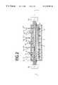
- FIG. 2is a cross section of the apparatus of FIG. 1
- FIG. 1showing an apparatus purely schematically in a longitudinal section
- FIG. 2showing it in cross section.
- the coating apparatusconsists essentially of two vacuum chambers 1 and 2 arranged in tandem, one of the chambers forming process chamber 1 , the slit airlocks 6 a and 6 b provided in the chamber walls, the transport devices 4 a and 4 b , a running substrate holder 3 , a plurality of gas inlet tubes 11 , 11 ′, 11 ′′ . . . and 11 a . . . , 11 b , joined together in the manner of a network, a corresponding number of gas outlet tubes 13 , 13 ′, 13 ′′ . . . and 13 a . . . 13 b , . . .
- the linear microwave plasma sources 9 , 9 ′, 9 ′′ . . .each fed by microwave transmitters 8 a , 8 b . . . , and a glow wire 7 , 7 ′, 7 ′′ . . . associated with each microwave plasma source 9 , 9 ′, 9 ′′ . . .
- the (flat) substrates 5are carried on the cooled substrate carrier 3 through the vacuum chamber 2 into the process chamber 1 through the slit airlocks 6 a and 6 b by means of the transport devices 4 a and 4 b .
- Precursor gasis fed to the coating process through the inlet tubes 11 , 11 ′, 11 ′′ . . . and 10 , 10 ′, 10 ′′ . . .
- the energy necessary for the coating processis delivered through a plurality of linear microplasma sources 9 , 9 ′, 9 ′′ . . . fed by microwave transmitters 8 a and 8 b , and a number of glow wires 7 , 7 ′, 7 ′′, 7 ′′′′ . . .
- the microwave plasma sources 9 , 9 ′, . . . and the glow wires 7 , 7 ′, 7 ′′, 7 ′′′′ . . .are arranged in alternating sequence, preferably equidistantly.
- the spacing of the glow wires 7 , 7 ′, 7 ′′, 7 ′′′′ . . . from the substrate surfaceis made to be smaller than the distances between the microwave plasma sources 9 , 9 ′, 9 ′′ . . . and the substrate 5 .
- the glow wires 7 , 7 ′, 7 ′′, 7 ′′′′ . . .are fed with a direct-current potential of electric currents.
- the power resulting from the direct-current voltages and the currentsis selected such that the temperatures of the glow wires are between 2000° C. and 3000° C.
- the voltages of the currents required for this purposedepend upon the geometry of the glow wires 7 , 7 ′, 7 ′′, 7 ′′′′ . . . (length and diameter) and on the glow wire material.
- the substrate 5 with the substrate holder 3can be moved periodically (in the direction of the broken double arrow) in order to optimize the uniformity of the coating process.
- a close network of gas inlet tubes 11 , 11 ′, 11 ′′ . . .be provided above the substrate surface to be coated, and surmounted by a likewise close network of gas outlet tubes 12 , 12 ′, 12 ′′, 12 ′′′′ . . . and 13 , 13 ′, 13 ′′ and 13 a , 13 b , 13 c . . . , both gas supply and connecting tubes as well as the tube sections extending across the plasma sources 9 , 9 ′, 9 ′′ . . . running parallel to one another, and tube sections perpendicular to the substrate plane, being provided for the input of gas and for gas extraction.
- the network of gas input and gas outletis constructed such that all parts of the substrate are exposed to approximately equal gas flows as well as plasma fields.
Landscapes
- Chemical & Material Sciences (AREA)
- General Chemical & Material Sciences (AREA)
- Chemical Kinetics & Catalysis (AREA)
- Engineering & Computer Science (AREA)
- Materials Engineering (AREA)
- Mechanical Engineering (AREA)
- Metallurgy (AREA)
- Organic Chemistry (AREA)
- Inorganic Chemistry (AREA)
- Chemical Vapour Deposition (AREA)
- Crystals, And After-Treatments Of Crystals (AREA)
Abstract
Description
Claims (2)
Applications Claiming Priority (3)
| Application Number | Priority Date | Filing Date | Title |
|---|---|---|---|
| DE19841777 | 1998-09-12 | ||
| DE19841777ADE19841777C1 (en) | 1998-09-12 | 1998-09-12 | Apparatus for plasma-technological precipitation of polycrystalline diamond on substrates with large plane areas |
| PCT/EP1999/006397WO2000016374A1 (en) | 1998-09-12 | 1999-09-01 | Device for the plasma deposition of a polycrystalline diamond |
Publications (1)
| Publication Number | Publication Date |
|---|---|
| US6487986B1true US6487986B1 (en) | 2002-12-03 |
Family
ID=7880738
Family Applications (1)
| Application Number | Title | Priority Date | Filing Date |
|---|---|---|---|
| US09/719,525Expired - Fee RelatedUS6487986B1 (en) | 1998-09-12 | 1999-09-01 | Device for the plasma deposition of a polycrystalline diamond |
Country Status (5)
| Country | Link |
|---|---|
| US (1) | US6487986B1 (en) |
| EP (1) | EP1127366B8 (en) |
| JP (1) | JP4195198B2 (en) |
| DE (2) | DE19841777C1 (en) |
| WO (1) | WO2000016374A1 (en) |
Cited By (16)
| Publication number | Priority date | Publication date | Assignee | Title |
|---|---|---|---|---|
| US20030177977A1 (en)* | 2000-09-22 | 2003-09-25 | Gerd Strauch | Gas-admission element for CVD processes, and device |
| US6681716B2 (en)* | 2001-11-27 | 2004-01-27 | General Electric Company | Apparatus and method for depositing large area coatings on non-planar surfaces |
| US20040112291A1 (en)* | 2000-04-12 | 2004-06-17 | Stirniman Michael Joseph | Single disc vapor lubrication |
| US20080296268A1 (en)* | 2007-06-01 | 2008-12-04 | Noritsu Koki Co., Ltd. | Plasma generator and workpiece processing apparatus using the same |
| US20120031335A1 (en)* | 2010-04-30 | 2012-02-09 | Applied Materials, Inc. | Vertical inline cvd system |
| GB2486779A (en)* | 2010-12-23 | 2012-06-27 | Element Six Ltd | A microwave plasma reactor for manufacturing synthetic diamond material |
| US20130192759A1 (en)* | 2010-08-02 | 2013-08-01 | Emd Corporation | Plasma processing device |
| US8859058B2 (en) | 2010-12-23 | 2014-10-14 | Element Six Limited | Microwave plasma reactors and substrates for synthetic diamond manufacture |
| US8955456B2 (en) | 2010-12-23 | 2015-02-17 | Element Six Limited | Microwave plasma reactor for manufacturing synthetic diamond material |
| US8980079B2 (en) | 2010-12-03 | 2015-03-17 | Electrolytic Ozone, Inc. | Electrolytic cell for ozone production |
| US9142389B2 (en) | 2010-12-23 | 2015-09-22 | Element Six Technologies Limited | Microwave power delivery system for plasma reactors |
| US20160032450A1 (en)* | 2013-03-28 | 2016-02-04 | Neocoat Sa | Method for a diamond vapor deposition |
| US9410242B2 (en) | 2010-12-23 | 2016-08-09 | Element Six Technologies Limited | Microwave plasma reactor for manufacturing synthetic diamond material |
| US9637838B2 (en) | 2010-12-23 | 2017-05-02 | Element Six Limited | Methods of manufacturing synthetic diamond material by microwave plasma enhanced chemical vapor deposition from a microwave generator and gas inlet(s) disposed opposite the growth surface area |
| US10403477B2 (en) | 2010-12-23 | 2019-09-03 | Element Six Technologies Limited | Microwave plasma reactor for manufacturing synthetic diamond material |
| US12442104B2 (en) | 2023-04-20 | 2025-10-14 | Applied Materials, Inc. | Nanocrystalline diamond with amorphous interfacial layer |
Families Citing this family (1)
| Publication number | Priority date | Publication date | Assignee | Title |
|---|---|---|---|---|
| KR20090088056A (en)* | 2008-02-14 | 2009-08-19 | 삼성전기주식회사 | Gas Supply Units and Chemical Vapor Deposition Devices |
Citations (6)
| Publication number | Priority date | Publication date | Assignee | Title |
|---|---|---|---|---|
| US5372648A (en)* | 1992-04-30 | 1994-12-13 | Matsushita Electric Industrial Co., Ltd. | Plasma CVD system |
| US5464476A (en)* | 1993-10-19 | 1995-11-07 | Central Research Laboratories Limited | Plasma processing device comprising plural RF inductive coils |
| US5510151A (en)* | 1989-06-28 | 1996-04-23 | Canon Kabushiki Kaisha | Continuous film-forming process using microwave energy in a moving substrate web functioning as a substrate and plasma generating space |
| DE19628949A1 (en) | 1995-02-02 | 1998-01-22 | Muegge Electronic Gmbh | Plasma generating device for vacuum container |
| EP0823493A1 (en) | 1996-08-05 | 1998-02-11 | Leybold Systems GmbH | Apparatus for plasma enhanced chemical vapour deposition of polycrystalline diamond |
| US5985378A (en)* | 1996-10-30 | 1999-11-16 | Schott Glaswerke | Remote-plasma-CVD method for coating or for treating large-surface substrates and apparatus for performing same |
Family Cites Families (2)
| Publication number | Priority date | Publication date | Assignee | Title |
|---|---|---|---|---|
| DE19503205C1 (en)* | 1995-02-02 | 1996-07-11 | Muegge Electronic Gmbh | Device for generating a plasma in low pressure container e.g. for hardware items surface treatment by plasma etching and plasma deposition |
| DE19722272A1 (en)* | 1997-05-28 | 1998-12-03 | Leybold Systems Gmbh | Device for generating plasma |
- 1998
- 1998-09-12DEDE19841777Apatent/DE19841777C1/ennot_activeExpired - Fee Related
- 1999
- 1999-09-01DEDE59912310Tpatent/DE59912310D1/ennot_activeExpired - Lifetime
- 1999-09-01JPJP2000570815Apatent/JP4195198B2/ennot_activeExpired - Fee Related
- 1999-09-01WOPCT/EP1999/006397patent/WO2000016374A1/enactiveIP Right Grant
- 1999-09-01USUS09/719,525patent/US6487986B1/ennot_activeExpired - Fee Related
- 1999-09-01EPEP99947272Apatent/EP1127366B8/ennot_activeExpired - Lifetime
Patent Citations (9)
| Publication number | Priority date | Publication date | Assignee | Title |
|---|---|---|---|---|
| US5510151A (en)* | 1989-06-28 | 1996-04-23 | Canon Kabushiki Kaisha | Continuous film-forming process using microwave energy in a moving substrate web functioning as a substrate and plasma generating space |
| US5372648A (en)* | 1992-04-30 | 1994-12-13 | Matsushita Electric Industrial Co., Ltd. | Plasma CVD system |
| US5464476A (en)* | 1993-10-19 | 1995-11-07 | Central Research Laboratories Limited | Plasma processing device comprising plural RF inductive coils |
| DE19628949A1 (en) | 1995-02-02 | 1998-01-22 | Muegge Electronic Gmbh | Plasma generating device for vacuum container |
| EP0823493A1 (en) | 1996-08-05 | 1998-02-11 | Leybold Systems GmbH | Apparatus for plasma enhanced chemical vapour deposition of polycrystalline diamond |
| JPH1088350A (en)* | 1996-08-05 | 1998-04-07 | Leybold Syst Gmbh | Apparatus for plasma-chemically precipitating polycrystalline diamond |
| US5900065A (en)* | 1996-08-05 | 1999-05-04 | Leybold Systems Gmbh | Apparatus for the plasma-chemical deposition of polycrystalline diamond |
| US5985378A (en)* | 1996-10-30 | 1999-11-16 | Schott Glaswerke | Remote-plasma-CVD method for coating or for treating large-surface substrates and apparatus for performing same |
| US6293222B1 (en)* | 1996-10-30 | 2001-09-25 | Schott Glaswerke | Remote-plasma-CVD method for coating or for treating large-surface substrates and apparatus for performing same |
Cited By (26)
| Publication number | Priority date | Publication date | Assignee | Title |
|---|---|---|---|---|
| US20130139754A1 (en)* | 2000-04-12 | 2013-06-06 | Seagate Technology Llc | Single disc vapor lubrication |
| US20040112291A1 (en)* | 2000-04-12 | 2004-06-17 | Stirniman Michael Joseph | Single disc vapor lubrication |
| US8728242B2 (en)* | 2000-04-12 | 2014-05-20 | Seagate Technology Llc | Single disc vapor lubrication |
| US8382902B2 (en)* | 2000-04-12 | 2013-02-26 | Seagate Technology Llc | Single disc vapor lubrication |
| US7294207B2 (en)* | 2000-09-22 | 2007-11-13 | Aixtron Ag | Gas-admission element for CVD processes, and device |
| US20030177977A1 (en)* | 2000-09-22 | 2003-09-25 | Gerd Strauch | Gas-admission element for CVD processes, and device |
| US6681716B2 (en)* | 2001-11-27 | 2004-01-27 | General Electric Company | Apparatus and method for depositing large area coatings on non-planar surfaces |
| US20080296268A1 (en)* | 2007-06-01 | 2008-12-04 | Noritsu Koki Co., Ltd. | Plasma generator and workpiece processing apparatus using the same |
| TWI551718B (en)* | 2010-04-30 | 2016-10-01 | 應用材料股份有限公司 | Vertical inline cvd system |
| US9324597B2 (en)* | 2010-04-30 | 2016-04-26 | Applied Materials, Inc. | Vertical inline CVD system |
| US20120031335A1 (en)* | 2010-04-30 | 2012-02-09 | Applied Materials, Inc. | Vertical inline cvd system |
| US20130192759A1 (en)* | 2010-08-02 | 2013-08-01 | Emd Corporation | Plasma processing device |
| US8980079B2 (en) | 2010-12-03 | 2015-03-17 | Electrolytic Ozone, Inc. | Electrolytic cell for ozone production |
| US8859058B2 (en) | 2010-12-23 | 2014-10-14 | Element Six Limited | Microwave plasma reactors and substrates for synthetic diamond manufacture |
| US8955456B2 (en) | 2010-12-23 | 2015-02-17 | Element Six Limited | Microwave plasma reactor for manufacturing synthetic diamond material |
| US9142389B2 (en) | 2010-12-23 | 2015-09-22 | Element Six Technologies Limited | Microwave power delivery system for plasma reactors |
| GB2486779B (en)* | 2010-12-23 | 2014-02-19 | Element Six Ltd | A microwave plasma reactor for manufacturing synthetic diamond material |
| US9410242B2 (en) | 2010-12-23 | 2016-08-09 | Element Six Technologies Limited | Microwave plasma reactor for manufacturing synthetic diamond material |
| GB2486779A (en)* | 2010-12-23 | 2012-06-27 | Element Six Ltd | A microwave plasma reactor for manufacturing synthetic diamond material |
| US9637838B2 (en) | 2010-12-23 | 2017-05-02 | Element Six Limited | Methods of manufacturing synthetic diamond material by microwave plasma enhanced chemical vapor deposition from a microwave generator and gas inlet(s) disposed opposite the growth surface area |
| US9738970B2 (en) | 2010-12-23 | 2017-08-22 | Element Six Limited | Microwave plasma reactors and substrates for synthetic diamond manufacture |
| US10403477B2 (en) | 2010-12-23 | 2019-09-03 | Element Six Technologies Limited | Microwave plasma reactor for manufacturing synthetic diamond material |
| US11371147B2 (en) | 2010-12-23 | 2022-06-28 | Element Six Technologies Limited | Microwave plasma reactor for manufacturing synthetic diamond material |
| US11488805B2 (en) | 2010-12-23 | 2022-11-01 | Element Six Technologies Limited | Microwave plasma reactor for manufacturing synthetic diamond material |
| US20160032450A1 (en)* | 2013-03-28 | 2016-02-04 | Neocoat Sa | Method for a diamond vapor deposition |
| US12442104B2 (en) | 2023-04-20 | 2025-10-14 | Applied Materials, Inc. | Nanocrystalline diamond with amorphous interfacial layer |
Also Published As
| Publication number | Publication date |
|---|---|
| JP2003527478A (en) | 2003-09-16 |
| EP1127366B8 (en) | 2005-11-09 |
| DE59912310D1 (en) | 2005-08-25 |
| DE19841777C1 (en) | 2000-01-05 |
| WO2000016374A1 (en) | 2000-03-23 |
| JP4195198B2 (en) | 2008-12-10 |
| EP1127366A1 (en) | 2001-08-29 |
| EP1127366B1 (en) | 2005-07-20 |
Similar Documents
| Publication | Publication Date | Title |
|---|---|---|
| US6487986B1 (en) | Device for the plasma deposition of a polycrystalline diamond | |
| US4566403A (en) | Apparatus for microwave glow discharge deposition | |
| US5554255A (en) | Method of and apparatus for a direct voltage arc discharge enhanced reactive treatment of objects | |
| US9165748B2 (en) | Plasma CVD method | |
| US20070262059A1 (en) | Electrode systems and methods of using electrodes | |
| EP3619734B1 (en) | Linear plasma source with segmented hollow cathode | |
| EP2080425B1 (en) | Device for forming a film by deposition from a plasma | |
| US5900065A (en) | Apparatus for the plasma-chemical deposition of polycrystalline diamond | |
| US5431968A (en) | Method for simultaneously coating a plurality of filaments | |
| CN101945689A (en) | System and method for pre-ionization of surface wave launched plasma discharge sources | |
| US4915978A (en) | Method and device for forming a layer by plasma-chemical process | |
| US8931433B2 (en) | Plasma processing apparatus | |
| US20100006142A1 (en) | Deposition apparatus for improving the uniformity of material processed over a substrate and method of using the apparatus | |
| JP4326419B2 (en) | Plasma processing apparatus and solar cell manufacturing method | |
| US9190249B2 (en) | Hollow cathode system, device and method for the plasma-assisted treatment of substrates | |
| JP3787444B2 (en) | Method and apparatus for forming semiconductor thin film | |
| JP3683999B2 (en) | Method and apparatus for forming non-single crystal semiconductor thin film | |
| JP3546095B2 (en) | Plasma CVD equipment | |
| JP2007191797A (en) | Film formation apparatus and film formation method | |
| JPH09232612A (en) | Non-single crystal semiconductor thin film forming apparatus and method |
Legal Events
| Date | Code | Title | Description |
|---|---|---|---|
| AS | Assignment | Owner name:BALZERS UND LEYBOLD DEUTSCHLAND HOLDING AG (FORMER Free format text:ASSIGNMENT OF ASSIGNORS INTEREST;ASSIGNORS:LIEHR, MICHAEL;SCHAFER, LOTHAR;REEL/FRAME:011489/0681;SIGNING DATES FROM 20001115 TO 20001204 Owner name:FRAUNHOFER-GESELLSCHAFT ZUR FORDERUNG DER ANGEWAND Free format text:ASSIGNMENT OF ASSIGNORS INTEREST;ASSIGNORS:LIEHR, MICHAEL;SCHAFER, LOTHAR;REEL/FRAME:011489/0681;SIGNING DATES FROM 20001115 TO 20001204 | |
| AS | Assignment | Owner name:UNAXIS DEUTSCHLAND HOLDING GMBH, GERMANY Free format text:CHANGE OF NAME;ASSIGNOR:BALZERS UND LEYBOLD DEUTSCHLAND HOLDING AG;REEL/FRAME:013863/0892 Effective date:20001205 | |
| FPAY | Fee payment | Year of fee payment:4 | |
| FEPP | Fee payment procedure | Free format text:PAYER NUMBER DE-ASSIGNED (ORIGINAL EVENT CODE: RMPN); ENTITY STATUS OF PATENT OWNER: LARGE ENTITY Free format text:PAYOR NUMBER ASSIGNED (ORIGINAL EVENT CODE: ASPN); ENTITY STATUS OF PATENT OWNER: LARGE ENTITY | |
| FPAY | Fee payment | Year of fee payment:8 | |
| REMI | Maintenance fee reminder mailed | ||
| LAPS | Lapse for failure to pay maintenance fees | ||
| STCH | Information on status: patent discontinuation | Free format text:PATENT EXPIRED DUE TO NONPAYMENT OF MAINTENANCE FEES UNDER 37 CFR 1.362 | |
| FP | Lapsed due to failure to pay maintenance fee | Effective date:20141203 |