US6486728B2 - Multi-stage charge pump - Google Patents
Multi-stage charge pumpDownload PDFInfo
- Publication number
- US6486728B2 US6486728B2US09/809,878US80987801AUS6486728B2US 6486728 B2US6486728 B2US 6486728B2US 80987801 AUS80987801 AUS 80987801AUS 6486728 B2US6486728 B2US 6486728B2
- Authority
- US
- United States
- Prior art keywords
- charge pump
- stage
- voltage output
- voltage
- stages
- Prior art date
- Legal status (The legal status is an assumption and is not a legal conclusion. Google has not performed a legal analysis and makes no representation as to the accuracy of the status listed.)
- Expired - Lifetime
Links
Images


Classifications
- H—ELECTRICITY
- H02—GENERATION; CONVERSION OR DISTRIBUTION OF ELECTRIC POWER
- H02M—APPARATUS FOR CONVERSION BETWEEN AC AND AC, BETWEEN AC AND DC, OR BETWEEN DC AND DC, AND FOR USE WITH MAINS OR SIMILAR POWER SUPPLY SYSTEMS; CONVERSION OF DC OR AC INPUT POWER INTO SURGE OUTPUT POWER; CONTROL OR REGULATION THEREOF
- H02M3/00—Conversion of DC power input into DC power output
- H02M3/02—Conversion of DC power input into DC power output without intermediate conversion into AC
- H02M3/04—Conversion of DC power input into DC power output without intermediate conversion into AC by static converters
- H02M3/06—Conversion of DC power input into DC power output without intermediate conversion into AC by static converters using resistors or capacitors, e.g. potential divider
- H02M3/07—Conversion of DC power input into DC power output without intermediate conversion into AC by static converters using resistors or capacitors, e.g. potential divider using capacitors charged and discharged alternately by semiconductor devices with control electrode, e.g. charge pumps
- H02M3/073—Charge pumps of the Schenkel-type
- H—ELECTRICITY
- H02—GENERATION; CONVERSION OR DISTRIBUTION OF ELECTRIC POWER
- H02M—APPARATUS FOR CONVERSION BETWEEN AC AND AC, BETWEEN AC AND DC, OR BETWEEN DC AND DC, AND FOR USE WITH MAINS OR SIMILAR POWER SUPPLY SYSTEMS; CONVERSION OF DC OR AC INPUT POWER INTO SURGE OUTPUT POWER; CONTROL OR REGULATION THEREOF
- H02M1/00—Details of apparatus for conversion
- H02M1/0003—Details of control, feedback or regulation circuits
- H02M1/0041—Control circuits in which a clock signal is selectively enabled or disabled
Definitions
- the present inventionrelates to multi-stage charge pumps suitable for use with integrated circuit applications.
- the charge pump described in U.S. Pat. No. 5,781,473is a multi-stage charge pump, and the output of each of the stages is connected directly to the high voltage output of the charge pump.
- the charge pump stagescan be configured to operate in parallel or in series, depending upon the state of various switches in the system.
- the charge pump described in U.S. Pat. No. 5,801,987is also a multiple stage charge pump in which one, two, three or four of the stages can be enabled.
- the outputs of all of the charge pump stagesare connected to the output of the charge pump via respective diodes. These diodes bring with them the disadvantage of a voltage drop across the diode even when the diode is conductive.
- the charge pumps described beloware multiple stage charge pumps that are connected in series, with stage one directly connected to the high voltage output of the charge pump and stages two and three and progressively farther from the high voltage output of the charge pump.
- the charge pump stagesare selectively enabled such that if charge pump stage m is enabled, then all charge pumps stages m ⁇ 1, . . . 1 are enabled. Depending upon the required output voltage, more or fewer of the charge pumps stages are enabled. This can be accomplished with a preprogrammed control circuit, or alternatively with an adaptive control circuit that responds to the output voltage of the charge pump.
- the embodiments described beloware relatively easy to implement, and they avoid diode drops in the chain of series-connected charge pump stages.
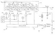
- FIG. 1is a block diagram of a charge pump and an associated oscillator that incorporate a first preferred embodiment of this invention.
- FIG. 1 ais a schematic diagram of one of the charge pump stages 14 a of FIG. 1 .
- FIG. 1 bis a schematic diagram of the oscillator of FIG. 1 .
- FIG. 2is a block diagram of a charge pump and an associated oscillator that incorporate a second preferred embodiment of this invention.
- FIG. 3is a block diagram of a charge pump, an oscillator, and a control circuit that incorporate a third preferred embodiment of this invention.
- FIG. 4is a block diagram of a fourth embodiment of this invention.
- the voltage source 10 of FIG. 1is formed on an integrated circuit substrate 12 that can, for example, be a conventional silicon die.
- the voltage source 10can, for example, be used to convert a 3-volt supply voltage V DD to a 10-volt output voltage as appropriate for use in programming an anti-fuse in a solid-state memory.
- the voltage source 10includes a charge pump 13 that in turn includes a set of series-connected charge pump stages 14 a - 14 d .
- the supply voltage V DDis applied to the lower voltage input of the charge pump 13 , and one, two, three, or all four of the stages 14 a - 14 d pump charge from the lower voltage input to the higher voltage output 22 .
- Each stageincludes a respective lower voltage input 16 a - 16 d , and a respective higher voltage output 18 a - 18 d .
- Each stage 14 a - 14 doperates to pump a unit of charge from its respective lower voltage input 16 a - 16 d to its respective higher voltage output 18 a - 18 d with each transition of the clock signal applied to the respective clock input 20 a - 20 d.
- the higher voltage output 18 a of the first stage 14 ais connected to a high voltage output 22 of the charge pump 13 .
- the higher voltage outputs 18 b , 18 c , 18 dare directly connected to the lower voltage inputs 16 a , 16 b , 16 c , respectively, such that the charge pump stages 14 a - 14 d are series connected.
- each of the lower voltage inputs 16 a - 16 dis connected to the supply voltage V DD .
- Switches 24 a - 24 cwhen open, isolate the respective lower voltage inputs 16 a - 16 c from the supply voltage V DD .
- FIG. 1 ais a schematic diagram of a charge pump stage which can be used for all of the stages 14 a - 14 d of FIG. 1 .
- the following U.S. patentsprovide other examples of the types of charge pumps that readily can be adapted for use in the voltage source of FIG. 1 :
- the rate at which charge is pumped by the charge pump 13 and the voltage to which it is pumpedare controlled by an oscillator 30 and a control circuit 50 .
- the oscillator 30generates five evenly spaced clock phases, and four of these five clock phases are applied to respective ones of the stages 14 a - 14 d as clock signals CLK 1 , CLK 2 , CLK 3 , and CLK 4 .
- the phase difference between the clock signals for each of the stages 14 a - 14 dis 2 ⁇ 5 per half cycle, which is close to the ideal 90° separation. Using more stages in the oscillator 30 allows closer to the optimal 90° spacing if desired.
- the oscillator 30is a voltage controlled oscillator.
- the frequency of oscillation of the oscillator 30is controlled by a control signal V CTRLP generated by differential amplifier 32 .
- the inverting input of the differential amplifier 32is held at a reference voltage BGAP, while the nonverting input of the amplifier 32 is coupled with a voltage divider that includes resistor R 1 , R 2 connected between the high voltage output 22 and ground.
- a decoupling capacitor 60is also connected to the high voltage output 22 in parallel with the voltage divider.
- Current drawn from the voltage source 10is indicated schematically by the load 70 , also connected to the high voltage output 22 .
- the target parameter used to control the frequency of the oscillator 30is not the frequency of the oscillator 30 , but rather the output voltage of the voltage source 10 .
- the feedback loop including the amplifier 32adjusts the frequency of the oscillator 30 to maintain a constant output voltage with low ripple for current loads that vary by several orders of magnitude.
- the oscillator 30responds to the control signal V CTRLP to alter the oscillation frequency as appropriate to maintain the voltage of the output 22 at the desired level.
- the frequency of oscillation of the oscillator 30is increased, thereby increasing the rate at which charge is pumped to the capacitor 70 .
- the oscillator 30reduces the frequency of oscillation of the clock signals, thereby lowering the rate at which charge is pumped to the capacitor 70 .
- the differential amplifier 32is one example of a feedback element, though many other approaches are possible.
- the feedback elementmay operate continuously or in a clocked manner, and it may include an amplifier (such as a differential amplifier) or another element that compares the signal V RATIO to a reference, as for example, a subtracting element.
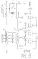
- FIG. 1 bprovides a circuit diagram of one embodiment of the oscillator 30 , though it should clearly be understood that many alternatives are possible. See, for example, the oscillators described in the following U.S. U.S. Pat. Nos. 4,859,968; 5,994,968; and 6,104,254.
- the control voltage V CTRLPis applied to FET 34 that controls the current passing through five FET's, one of which is labeled with the reference symbol 35 .
- FET 34is coupled with a second FET 36 that controls the current passing through five FETs, one of which is designated with the reference symbol 37 .
- the oscillator 30includes five inverters, one of which includes the FET's 38 , 39 . Each inverter is characterized by a delay period that varies as a function of the state of conduction of the associated FET's 35 , 37 .
- the control circuit 50 of FIG. 1operates to enable selected ones of the stages 14 b - 14 d .
- the control circuit 50includes NOR gates 52 b , 52 c , 52 d as well as a programmable register 54 that stores three control parameters E 1 , E 2 , E 3 .
- the register 54may be programmed during fabrication or during operation to set the logic state of the parameters E 1 -E 3 .
- Logic signals generated in response to the stored parameters of the register 54are also applied to the switches 24 a , 24 b , 24 c , as shown in FIG. 1 .
- the stored parameter E 3is in the logic high state and the stored parameters E 1 and E 2 are in the logic low state.
- the stage 14 dis disabled, while the stages 14 a , 14 b , and 14 c are enabled.
- the switches 24 a , 24 bare in the open-circuit state, and the switch 24 c is in the closed-circuit state.
- charge pumped from V DD to the high voltage output 22is pumped to a lesser voltage in an efficient manner.
- stored parameters E 3 , E 2are in the logic high state and stored parameter E 1 is in the logic low state.
- the stages 14 d and 14 care disabled while the stages 14 b and 14 a are enabled.
- the switch 24 ais in the open-circuit condition, while the switches 24 b and 24 c are in the closed-circuit condition. In this mode of operation, charge is pumped successively through only two stages 14 a , 14 b before being supplied to the high voltage output 22 of the charge pump 13 .
- a fourth mode of operationall three of the stored parameters E 1 , E 2 , E 3 are in the logic high state, and only the stage 14 a is enabled.
- the switch 24 ais in the closed-circuit state, and charge passes through only a single stage 14 a before being delivered to the high voltage output 22 .
- control circuit 50can be used to alter the number of stages 14 a - 14 d that are activated in order to optimize charge pump efficiency for a given voltage and current target.
- the ratio R 1 /R 2 and the band gap voltage BGAPset the voltage level V HIGH of the voltage source without any external components off the substrate 12 .
- All of the components of FIG. 1(except perhaps for the load 22 ) are built on the same integrated circuit substrate 12 , and no external components are required to achieve a low ripple voltage.
- the control method implemented by the circuit of FIG. 1provides a particularly efficient way of altering the number of stages operating to pump charge at any time, because it avoids the need for diodes and the associated diode or transistor voltage drops of certain prior-art devices.
- the phases of the clock signals of the adjacent charge pump stagesare chosen to achieve approximately a 90° phase offset between adjacent stages, thereby optimizing efficiency.
- the exact phaseis not critical, and elaborate clock drivers used to insure non-overlapping clock signals are not required. This further simplifies layout, since the routing of the clock phases is not critical and can be done with minimum pitch to reduce layout and power requirements.
- the register 54may be rewriteable, in which case the parameters E 1 , E 2 , E 3 can be changed in accordance with operating conditions.
- the register 54may be a write-once register, in which case the parameters E 1 , E 2 , E 3 may be set at or after the time of circuit fabrication.
- FIG. 2shows an alternative embodiment of this invention that operates similarly to the embodiment of FIG. 1 .
- multiple charge pumps 13 , 13 a , 13 b , 13 care provided, all connected in parallel to the high voltage output 22 .
- the use of multiple, parallel charge pumpsfurther reduces ripple voltages at the high voltage output 22 .
- the various charge pumpscan be driven in parallel, or alternatively the clock phases can be inverted between adjacent charge pumps or buffered within each charge pump. Inverting or buffering the clock signals in each charge pump reduces the peak-to-average current drawn from the power supply, which reduces noise and improves efficiency.
- the charge pumps 13 , 13 a , 13 b , 13 care connected in parallel, and clock and enable lines are cascaded to reduce the load on each clock enable line and thereby to simplify layout.
- the charge pump of this inventionbe used in combination with a voltage controlled oscillator.
- the oscillator 30 ′is similar to the oscillator 30 described above, except that the control voltage V CTRLP is maintained at a constant level.
- the control circuit 50 ′is implemented as four flip flops 56 a - 56 d and four associated AND gates 58 a - 58 d .
- Each of the flip flops 56 a - 56 dincludes a respective clock input connected to CLK 1 , a respective D input and a respective Q output.
- the D input of the flip flop 56 dis controlled by an inverter 59 coupled to the output of the amplifier 32 .
- the amplifier 32functions as a simple on/off comparator. Depending upon the voltage on the high voltage output 22 , the output of the amplifier 32 is either high or low. In particular, when the voltage on the high voltage output 22 exceeds a first threshold, the output of the amplifier 32 is high and the enable signal applied to the D input of the flip flops 56 d is low.
- This enable signalis latched and cascaded via flip flops 56 c , 56 b , 56 d to progressively disable the clock signals CLK 4 , CLK 3 , CLK 2 , CLK 1 in the stated order.
- Thisprogressively reduces the voltage of charge pumped by the charge pump 13 , eventually resulting in a reduction in the voltage V HIGH at the output 22 .
- a second thresholdwhich may be the same as or different from the first threshold
- the output of the amplifier 32goes low, and the enable signal applied to the D input of the flip flop 56 d goes high. This high state of the enable signal is latched and cascaded as described above to progressively enable all four stages of the charge pump 13 .
- FIG. 4shows a fourth embodiment which combines features of the embodiments of FIGS. 1 and 3 described above.
- a voltage controlled oscillatoris used to vary the clock frequency as a function of the output V HIGH , and the charge pump enable signal cascades through a series of flip flops.
- stage 14 aa smaller number of stages starting with stage 14 a is enabled, as for example when the output voltage V HIGH exceeds the first threshold or when the parameters E 1 -E 3 are in a first programmed state.
- a larger number of stagesis enabled, again beginning with the stage 14 a . This can be appropriate for example when the output voltage V HIGH is less than a second threshold or when the parameters E 1 -E 3 are in a second programmed state.
- the number of charge pump stagescan be varied widely, and it can include two, three, four or more. In general, the use of more charge pumps in parallel will lower the voltage ripple.
- the delay element used in the oscillatorcan also be varied widely. The illustrated delay element has the advantage of not consuming DC power so that a frequency proportional to the output load is easily achieved.
- the resistors R 1 , R 2can be implemented as switched capacitor resistors to reduce the power further as the frequency is reduced.
- a wide variety of charge pump constructionscan be used, though the illustrated differential charge pump provides the advantage of reduced ripple.
- the integrated charge pumps described aboveprovide the advantage of low output ripple voltage for a wide range load currents, small charge storage devices such as a decoupling capacitor that can readily be placed on the substrate, efficient operation over a wide range of current loads and a small peak-to-average current drawn from the power supply.
- Coupled withis intended broadly to refer to elements that are coupled together directly or indirectly. Thus, first and second elements are said to be coupled with one another, whether or not a third, unnamed element is interposed between the first and second elements.
- clock signalis used to indicate a set of clock signals.
- the clock signal applied to each charge pump stagemay include one, two, or more separate signals.
- a charge pump stageis intended broadly to encompass any suitable method for selectively allowing a charge pump stage to pump charge, as for example by turning on a clock signal and/or by connecting the charge pump stage to a charge source.
Landscapes
- Engineering & Computer Science (AREA)
- Power Engineering (AREA)
- Dc-Dc Converters (AREA)
Abstract
Description
Claims (11)
Priority Applications (1)
| Application Number | Priority Date | Filing Date | Title |
|---|---|---|---|
| US09/809,878US6486728B2 (en) | 2001-03-16 | 2001-03-16 | Multi-stage charge pump |
Applications Claiming Priority (1)
| Application Number | Priority Date | Filing Date | Title |
|---|---|---|---|
| US09/809,878US6486728B2 (en) | 2001-03-16 | 2001-03-16 | Multi-stage charge pump |
Publications (2)
| Publication Number | Publication Date |
|---|---|
| US20020130701A1 US20020130701A1 (en) | 2002-09-19 |
| US6486728B2true US6486728B2 (en) | 2002-11-26 |
Family
ID=25202403
Family Applications (1)
| Application Number | Title | Priority Date | Filing Date |
|---|---|---|---|
| US09/809,878Expired - LifetimeUS6486728B2 (en) | 2001-03-16 | 2001-03-16 | Multi-stage charge pump |
Country Status (1)
| Country | Link |
|---|---|
| US (1) | US6486728B2 (en) |
Cited By (113)
| Publication number | Priority date | Publication date | Assignee | Title |
|---|---|---|---|---|
| US20030227294A1 (en)* | 2002-06-06 | 2003-12-11 | Mecier Richard A. | Programming circuit and method having extended duration programming capabilities |
| US20040070999A1 (en)* | 2002-10-09 | 2004-04-15 | Intersil Americas Inc. | Charge pump drive signal recovery circuit |
| US20040155699A1 (en)* | 2002-02-21 | 2004-08-12 | Blodgett Greg A. | Capacitor charge sharing charge pump |
| US6816001B2 (en)* | 2001-11-09 | 2004-11-09 | Stmicroelectronics S.R.L. | Low power charge pump circuit |
| US20040250183A1 (en)* | 2003-02-11 | 2004-12-09 | Crowley Matthew P. | System architecture and method for three-dimensional memory |
| US20040263238A1 (en)* | 2003-06-30 | 2004-12-30 | Matrix Semiconductor, Inc. | Charge pump circuit incorporating corresponding parallel charge pump stages and method therefor |
| US20050052220A1 (en)* | 2003-09-08 | 2005-03-10 | Burgener Mark L. | Low noise charge pump method and apparatus |
| US20050189982A1 (en)* | 2004-02-27 | 2005-09-01 | Broadcom Corporation | Regulated charge pump with digital resistance control |
| US20050195019A1 (en)* | 2004-03-08 | 2005-09-08 | Nec Electronics Corporation | Booster circuit and semiconductor device having same |
| US20050213267A1 (en)* | 2004-03-25 | 2005-09-29 | Integral Wave Technologies, Inc. | Switched-capacitor power supply system and method |
| US20050213280A1 (en)* | 2004-03-25 | 2005-09-29 | Integral Wave Technologies, Inc. | Trench capacitor power supply system and method |
| US20060186947A1 (en)* | 2005-02-24 | 2006-08-24 | Macronix International Co., Ltd. | Multi-stage charge pump without threshold drop with frequency modulation between embedded mode operations |
| US20060250177A1 (en)* | 2005-05-09 | 2006-11-09 | Thorp Tyler J | Methods and apparatus for dynamically reconfiguring a charge pump during output transients |
| US20070069801A1 (en)* | 2005-05-20 | 2007-03-29 | Stmicroelectronics S.R.L. | Charge-pump type, voltage-boosting device with reduced ripple, in particular for non-volatile flash memories |
| US20070211502A1 (en)* | 2006-03-07 | 2007-09-13 | Kunihiro Komiya | Voltage step-up circuit and electric appliance therewith |
| US20080012627A1 (en)* | 2006-07-13 | 2008-01-17 | Yosuke Kato | System and method for low voltage booster circuits |
| US20080024198A1 (en)* | 2006-07-28 | 2008-01-31 | Stmicroelectronics S.R.I. | Voltage booster |
| US20080036528A1 (en)* | 2006-08-10 | 2008-02-14 | Elite Semiconductor Memory Technology Inc. | Charge pump circuit |
| US20080054990A1 (en)* | 2006-08-30 | 2008-03-06 | Taiwan Semiconductor Manufacturing Co., Ltd. | Charge pump method and architecture |
| US20080157852A1 (en)* | 2006-12-29 | 2008-07-03 | Sandisk Corporation | Unified voltage generation apparatus with improved power efficiency |
| US20080157854A1 (en)* | 2006-12-31 | 2008-07-03 | Al-Shamma Ali K | Multiple polarity reversible charge pump circuit |
| US20080157853A1 (en)* | 2006-12-31 | 2008-07-03 | Al-Shamma Ali K | Method for using a multiple polarity reversible charge pump circuit |
| US20080239836A1 (en)* | 2007-03-30 | 2008-10-02 | Tyler Thorp | Method for Managing Electrical Load of an Electronic Device |
| US20080239802A1 (en)* | 2007-03-30 | 2008-10-02 | Tyler Thorp | Device with Load-Based Voltage Generation |
| US20080239856A1 (en)* | 2007-03-30 | 2008-10-02 | Tyler Thorp | Method for Load-Based Voltage Generation |
| US20080239801A1 (en)* | 2007-03-30 | 2008-10-02 | Tyler Thorp | Load Management for Memory Device |
| US7440342B2 (en) | 2006-12-29 | 2008-10-21 | Sandisk Corporation | Unified voltage generation method with improved power efficiency |
| US20080272832A1 (en)* | 2007-05-02 | 2008-11-06 | Samsung Electronics Co., Ltd. | Charge pump circuit and method of controlling the same |
| US20080315848A1 (en)* | 2007-06-20 | 2008-12-25 | Atmel Corporation | Voltage regulator for an integrated circuit |
| US20090066407A1 (en)* | 2007-09-12 | 2009-03-12 | Rochester Institute Of Technology | Charge pump systems and methods thereof |
| US20090128212A1 (en)* | 2007-11-21 | 2009-05-21 | O2Micro, Inc. | Charge pump systems with adjustable frequency control |
| US20090153231A1 (en)* | 2007-12-12 | 2009-06-18 | Feng Pan | Diode Connected Regulation of Charge Pumps |
| US20090153230A1 (en)* | 2007-12-12 | 2009-06-18 | Feng Pan | Low Voltage Charge Pump with Regulation |
| US20090302930A1 (en)* | 2008-06-09 | 2009-12-10 | Feng Pan | Charge Pump with Vt Cancellation Through Parallel Structure |
| US7683700B2 (en) | 2008-06-25 | 2010-03-23 | Sandisk Corporation | Techniques of ripple reduction for charge pumps |
| US20100148856A1 (en)* | 2008-12-17 | 2010-06-17 | Man Lung Lui | Regulation of Recovery Rates in Charge Pumps |
| US7795951B2 (en) | 2007-11-30 | 2010-09-14 | Freescale Semiconductor, Inc. | High-dynamic range low ripple voltage multiplier |
| US20100308899A1 (en)* | 2009-06-04 | 2010-12-09 | Pericom Semiconductor Corp. | Dual-Output Triple-Vdd Charge Pump |
| US20100315132A1 (en)* | 2008-01-08 | 2010-12-16 | Gebara Fadi H | Peak power reduction methods in distributed charge pump systems |
| US20110115552A1 (en)* | 2008-03-24 | 2011-05-19 | Renesas Electronics Corporation | Charge pump circuit |
| US7969235B2 (en) | 2008-06-09 | 2011-06-28 | Sandisk Corporation | Self-adaptive multi-stage charge pump |
| US7973592B2 (en) | 2009-07-21 | 2011-07-05 | Sandisk Corporation | Charge pump with current based regulation |
| US8013666B1 (en)* | 2009-07-31 | 2011-09-06 | Altera Corporation | Low ripple charge pump |
| US8044705B2 (en) | 2007-08-28 | 2011-10-25 | Sandisk Technologies Inc. | Bottom plate regulation of charge pumps |
| US20110309877A1 (en)* | 2010-06-21 | 2011-12-22 | Rf Micro Devices, Inc. | High voltage charge-pump with a novel feedback control loop |
| US20120063250A1 (en)* | 2010-07-20 | 2012-03-15 | Macronix International Co., Ltd. | Non-volatile memory device and charge pump circuit for the same |
| WO2012087518A2 (en) | 2010-12-20 | 2012-06-28 | Sandisk 3D Llc | Charge pump system that dynamically selects number of active stages |
| WO2012087532A1 (en) | 2010-12-20 | 2012-06-28 | Sandisk Technologies Inc. | Charge pump systems with reduction in inefficiencies due to charge sharing between capacitances |
| US20120313694A1 (en)* | 2011-06-09 | 2012-12-13 | Yu-Jong Noh | Internal voltage generation circuit and operation method thereof |
| US8339183B2 (en) | 2009-07-24 | 2012-12-25 | Sandisk Technologies Inc. | Charge pump with reduced energy consumption through charge sharing and clock boosting suitable for high voltage word line in flash memories |
| WO2013036342A1 (en) | 2011-09-09 | 2013-03-14 | Sandisk Technologies Inc. | Charge pump system dynamically reconfigurable for read and program |
| US8400212B1 (en) | 2011-09-22 | 2013-03-19 | Sandisk Technologies Inc. | High voltage charge pump regulation system with fine step adjustment |
| US20130162229A1 (en)* | 2011-04-27 | 2013-06-27 | Realtek Semiconductor Corp. | Charge pump feedback control device and method using the same |
| US8514628B2 (en) | 2011-09-22 | 2013-08-20 | Sandisk Technologies Inc. | Dynamic switching approach to reduce area and power consumption of high voltage charge pumps |
| CN101576754B (en)* | 2008-05-08 | 2013-10-30 | 三星电子株式会社 | Charge pump circuit and method for controlling same |
| US20140022005A1 (en)* | 2012-07-23 | 2014-01-23 | Freescale Semiconductor, Inc. | Configurable multistage charge pump using a supply detect scheme |
| US8686787B2 (en) | 2011-05-11 | 2014-04-01 | Peregrine Semiconductor Corporation | High voltage ring pump with inverter stages and voltage boosting stages |
| US8710907B2 (en) | 2008-06-24 | 2014-04-29 | Sandisk Technologies Inc. | Clock generator circuit for a charge pump |
| US8710909B2 (en) | 2012-09-14 | 2014-04-29 | Sandisk Technologies Inc. | Circuits for prevention of reverse leakage in Vth-cancellation charge pumps |
| US8724353B1 (en) | 2013-03-15 | 2014-05-13 | Arctic Sand Technologies, Inc. | Efficient gate drivers for switched capacitor converters |
| US8817501B1 (en) | 2013-03-15 | 2014-08-26 | Arctic Sand Technologies, Inc. | Reconfigurable switched capacitor power converter techniques |
| US8836412B2 (en) | 2013-02-11 | 2014-09-16 | Sandisk 3D Llc | Charge pump with a power-controlled clock buffer to reduce power consumption and output voltage ripple |
| US8860396B2 (en) | 2011-05-05 | 2014-10-14 | Arctic Sand Technologies, Inc. | DC-DC converter with modular stages |
| US20150070081A1 (en)* | 2013-09-06 | 2015-03-12 | Texas Instruments Deutschland Gmbh | System and method for reduction of bottom plate parasitic capacitance in charge pumps |
| US20150070080A1 (en)* | 2013-09-06 | 2015-03-12 | Texas Instruments Deutschland Gmbh | System and method for distributed regulation of charge pumps |
| US8981835B2 (en) | 2013-06-18 | 2015-03-17 | Sandisk Technologies Inc. | Efficient voltage doubler |
| US8994452B2 (en) | 2008-07-18 | 2015-03-31 | Peregrine Semiconductor Corporation | Low-noise high efficiency bias generation circuits and method |
| US9007046B2 (en) | 2013-06-27 | 2015-04-14 | Sandisk Technologies Inc. | Efficient high voltage bias regulation circuit |
| US9024680B2 (en) | 2013-06-24 | 2015-05-05 | Sandisk Technologies Inc. | Efficiency for charge pumps with low supply voltages |
| US9041459B2 (en) | 2013-09-16 | 2015-05-26 | Arctic Sand Technologies, Inc. | Partial adiabatic conversion |
| US9077238B2 (en) | 2013-06-25 | 2015-07-07 | SanDisk Technologies, Inc. | Capacitive regulation of charge pumps without refresh operation interruption |
| US9083231B2 (en) | 2013-09-30 | 2015-07-14 | Sandisk Technologies Inc. | Amplitude modulation for pass gate to improve charge pump efficiency |
| US9093129B2 (en) | 2011-09-01 | 2015-07-28 | Chengdu Haicun Ip Technology Llc | Discrete three-dimensional memory comprising dice with different BEOL structures |
| US9154027B2 (en) | 2013-12-09 | 2015-10-06 | Sandisk Technologies Inc. | Dynamic load matching charge pump for reduced current consumption |
| US9264053B2 (en) | 2011-01-18 | 2016-02-16 | Peregrine Semiconductor Corporation | Variable frequency charge pump |
| US9491151B2 (en) | 2015-01-07 | 2016-11-08 | Ememory Technology Inc. | Memory apparatus, charge pump circuit and voltage pumping method thereof |
| US9520776B1 (en) | 2015-09-18 | 2016-12-13 | Sandisk Technologies Llc | Selective body bias for charge pump transfer switches |
| US9647536B2 (en) | 2015-07-28 | 2017-05-09 | Sandisk Technologies Llc | High voltage generation using low voltage devices |
| US9660520B2 (en) | 2013-04-09 | 2017-05-23 | Massachusetts Institute Of Technology | Method and apparatus to provide power conversion with high power factor |
| US9660590B2 (en) | 2008-07-18 | 2017-05-23 | Peregrine Semiconductor Corporation | Low-noise high efficiency bias generation circuits and method |
| US9667139B2 (en) | 2008-05-08 | 2017-05-30 | Massachusetts Institute Of Technology | Power converter with capacitive energy transfer and fast dynamic response |
| US9742266B2 (en) | 2013-09-16 | 2017-08-22 | Arctic Sand Technologies, Inc. | Charge pump timing control |
| US9825545B2 (en) | 2013-10-29 | 2017-11-21 | Massachusetts Institute Of Technology | Switched-capacitor split drive transformer power conversion circuit |
| US9847712B2 (en) | 2013-03-15 | 2017-12-19 | Peregrine Semiconductor Corporation | Fault control for switched capacitor power converter |
| US9882471B2 (en) | 2011-05-05 | 2018-01-30 | Peregrine Semiconductor Corporation | DC-DC converter with modular stages |
| US9887622B2 (en) | 2014-03-14 | 2018-02-06 | Peregrine Semiconductor Corporation | Charge pump stability control |
| US9917507B2 (en) | 2015-05-28 | 2018-03-13 | Sandisk Technologies Llc | Dynamic clock period modulation scheme for variable charge pump load currents |
| US10033271B1 (en) | 2016-12-30 | 2018-07-24 | Texas Instruments Incorporated | Multi-stage charge pump |
| US10075064B2 (en) | 2014-07-03 | 2018-09-11 | Massachusetts Institute Of Technology | High-frequency, high density power factor correction conversion for universal input grid interface |
| US10128745B2 (en) | 2014-03-14 | 2018-11-13 | Psemi Corporation | Charge balanced charge pump control |
| US10193441B2 (en) | 2015-03-13 | 2019-01-29 | Psemi Corporation | DC-DC transformer with inductor for the facilitation of adiabatic inter-capacitor charge transport |
| US10236770B1 (en)* | 2017-11-27 | 2019-03-19 | National Chiao Tung University | High-voltage generator with multi-stage selection in low-voltage transistor process |
| US10312791B1 (en) | 2018-07-02 | 2019-06-04 | National Chiao Tung University | Negative high-voltage generation device with multi-stage selection |
| US10389235B2 (en) | 2011-05-05 | 2019-08-20 | Psemi Corporation | Power converter |
| CN110168467A (en)* | 2019-04-10 | 2019-08-23 | 长江存储科技有限责任公司 | Reconfigurable voltage regulator |
| EP3557741A1 (en)* | 2018-04-16 | 2019-10-23 | ams International AG | Charge pump circuit and method for voltage conversion |
| US10666134B2 (en) | 2013-03-15 | 2020-05-26 | Psemi Corporation | Fault control for switched capacitor power converter |
| US10680515B2 (en) | 2011-05-05 | 2020-06-09 | Psemi Corporation | Power converters with modular stages |
| US10680513B2 (en) | 2012-11-26 | 2020-06-09 | Psemi Corporation | Pump capacitor configuration for voltage multiplier |
| US10686380B2 (en) | 2011-12-19 | 2020-06-16 | Psemi Corporation | Switched-capacitor circuit control in power converters |
| US10686367B1 (en) | 2019-03-04 | 2020-06-16 | Psemi Corporation | Apparatus and method for efficient shutdown of adiabatic charge pumps |
| US10693368B2 (en) | 2014-03-14 | 2020-06-23 | Psemi Corporation | Charge pump stability control |
| US20210210122A1 (en)* | 2018-09-26 | 2021-07-08 | Micron Technology, Inc. | Charge pump supply optimization and noise reduction method for logic systems |
| TWI733333B (en)* | 2019-10-18 | 2021-07-11 | 台灣積體電路製造股份有限公司 | System and method for providing low ripple voltage signal and memory system |
| US11127474B2 (en) | 2019-12-31 | 2021-09-21 | Samsung Electronics Co., Ltd. | Memory device |
| US11270177B2 (en) | 2019-10-02 | 2022-03-08 | Nxp B.V. | RFID transponder and corresponding operating method |
| US20220263408A1 (en)* | 2021-02-18 | 2022-08-18 | SK Hynix Inc. | Charge pump circuit, operating method thereof and semiconductor device including charge pump circuit |
| US11509214B2 (en)* | 2018-04-26 | 2022-11-22 | Micron Technology, Inc. | Apparatuses and methods for controlling charge pump circuits |
| US20230402916A1 (en)* | 2022-06-10 | 2023-12-14 | SK Hynix Inc. | Charge pump circuit related to overvoltage |
| US12107495B2 (en) | 2015-07-08 | 2024-10-01 | Psemi Corporation | Switched-capacitor power converters |
| US12272419B2 (en) | 2022-10-12 | 2025-04-08 | Samsung Electronics Co., Ltd. | Charge pump having switch circuits for blocking leakage current during sudden power-off, and flash memory including the same |
| US12328066B2 (en) | 2020-01-09 | 2025-06-10 | Skyworks Solutions, Inc. | Low noise charge pumps |
| US12438135B2 (en) | 2011-10-18 | 2025-10-07 | Psemi Corporation | Multilayer power, converter with devices having reduced lateral current |
Families Citing this family (31)
| Publication number | Priority date | Publication date | Assignee | Title |
|---|---|---|---|---|
| US6927441B2 (en)* | 2001-03-20 | 2005-08-09 | Stmicroelectronics S.R.L. | Variable stage charge pump |
| US7180322B1 (en) | 2002-04-16 | 2007-02-20 | Transmeta Corporation | Closed loop feedback control of integrated circuits |
| US7941675B2 (en) | 2002-12-31 | 2011-05-10 | Burr James B | Adaptive power control |
| ITMI20021902A1 (en)* | 2002-09-06 | 2004-03-07 | Atmel Corp | MODULAR CHARGE PUMP ARCHITECTURE |
| US6788130B2 (en)* | 2002-09-25 | 2004-09-07 | Texas Instruments Incorporated | Efficient charge pump capable of high voltage operation |
| ITMI20022268A1 (en)* | 2002-10-25 | 2004-04-26 | Atmel Corp | VARIABLE CHARGE PUMP CIRCUIT WITH DYNAMIC LOAD |
| US7228242B2 (en) | 2002-12-31 | 2007-06-05 | Transmeta Corporation | Adaptive power control based on pre package characterization of integrated circuits |
| US7953990B2 (en) | 2002-12-31 | 2011-05-31 | Stewart Thomas E | Adaptive power control based on post package characterization of integrated circuits |
| US6878981B2 (en)* | 2003-03-20 | 2005-04-12 | Tower Semiconductor Ltd. | Triple-well charge pump stage with no threshold voltage back-bias effect |
| KR100572323B1 (en)* | 2003-12-11 | 2006-04-19 | 삼성전자주식회사 | Multilevel High Voltage Generator |
| US7692477B1 (en) | 2003-12-23 | 2010-04-06 | Tien-Min Chen | Precise control component for a substrate potential regulation circuit |
| US7129771B1 (en) | 2003-12-23 | 2006-10-31 | Transmeta Corporation | Servo loop for well bias voltage source |
| US7012461B1 (en) | 2003-12-23 | 2006-03-14 | Transmeta Corporation | Stabilization component for a substrate potential regulation circuit |
| US7649402B1 (en)* | 2003-12-23 | 2010-01-19 | Tien-Min Chen | Feedback-controlled body-bias voltage source |
| JP4257196B2 (en)* | 2003-12-25 | 2009-04-22 | 株式会社東芝 | Semiconductor device and driving method of semiconductor device |
| US20050286278A1 (en)* | 2004-04-22 | 2005-12-29 | Perreault David J | Method and apparatus for switched-mode power conversion at radio frequencies |
| US7562233B1 (en) | 2004-06-22 | 2009-07-14 | Transmeta Corporation | Adaptive control of operating and body bias voltages |
| US7774625B1 (en) | 2004-06-22 | 2010-08-10 | Eric Chien-Li Sheng | Adaptive voltage control by accessing information stored within and specific to a microprocessor |
| WO2008086396A2 (en) | 2007-01-09 | 2008-07-17 | Power Monitors Inc. | Method and apparatus for smart circuit breaker |
| WO2009111386A2 (en) | 2008-03-04 | 2009-09-11 | Power Monitors, Inc. | Method and apparatus for a voice-prompted electrical hookup |
| KR100968467B1 (en)* | 2008-12-30 | 2010-07-07 | 주식회사 하이닉스반도체 | Circuit for voltage pump and semiconductor memory device using the same |
| US8773108B2 (en) | 2009-11-10 | 2014-07-08 | Power Monitors, Inc. | System, method, and apparatus for a safe powerline communications instrumentation front-end |
| US10060957B2 (en) | 2010-07-29 | 2018-08-28 | Power Monitors, Inc. | Method and apparatus for a cloud-based power quality monitor |
| EP3324153A1 (en) | 2010-07-29 | 2018-05-23 | Power Monitors, Inc. | Method and apparatus for a demand management monitoring system |
| US8587367B1 (en)* | 2012-06-06 | 2013-11-19 | Nanya Technology Corp. | Voltage pumping circuit |
| KR20160097403A (en)* | 2015-02-06 | 2016-08-18 | 에스케이하이닉스 주식회사 | Internal voltage generator and operation method thereof |
| US11190182B2 (en)* | 2017-02-13 | 2021-11-30 | Skyworks Solutions, Inc. | Control circuitry for silicon-on-insulator chip |
| CN107317469A (en)* | 2017-07-11 | 2017-11-03 | 风华研究院(广州)有限公司 | Driving voltage adaptive circuit |
| CN109980919B (en)* | 2017-12-27 | 2020-07-10 | 北京兆易创新科技股份有限公司 | Charge pump system |
| WO2020113406A1 (en) | 2018-12-04 | 2020-06-11 | Micron Technology, Inc. | Multi-mode voltage pump and control |
| WO2020240242A1 (en)* | 2019-05-31 | 2020-12-03 | Micron Technology, Inc. | Intelligent charge pump architecture for flash array |
Citations (12)
| Publication number | Priority date | Publication date | Assignee | Title |
|---|---|---|---|---|
| US5216588A (en) | 1992-02-14 | 1993-06-01 | Catalyst Semiconductor, Inc. | Charge pump with high output current |
| US5357216A (en) | 1993-01-13 | 1994-10-18 | National Semiconductor Corporation | Current sourcing and sinking circuit for driving a VCO charge pump |
| US5553030A (en) | 1993-09-10 | 1996-09-03 | Intel Corporation | Method and apparatus for controlling the output voltage provided by a charge pump circuit |
| US5627739A (en) | 1996-04-02 | 1997-05-06 | Winbond Electronics Corp. | Regulated charge pump with low noise on the well of the substrate |
| US5635776A (en) | 1992-02-27 | 1997-06-03 | Texas Instruments Incorporated | Charge pump voltage converter |
| US5680300A (en) | 1995-12-22 | 1997-10-21 | Analog Devices, Inc. | Regulated charge pump DC/DC converter |
| US5781473A (en) | 1995-09-29 | 1998-07-14 | Intel Corporation | Variable stage charge pump |
| US5801987A (en) | 1997-03-17 | 1998-09-01 | Motorola, Inc. | Automatic transition charge pump for nonvolatile memories |
| US5912552A (en) | 1997-02-12 | 1999-06-15 | Kabushiki Kaisha Toyoda Jidoshokki Seisakusho | DC to DC converter with high efficiency for light loads |
| US5994885A (en) | 1993-03-23 | 1999-11-30 | Linear Technology Corporation | Control circuit and method for maintaining high efficiency over broad current ranges in a switching regulator circuit |
| US6157242A (en)* | 1998-03-19 | 2000-12-05 | Sharp Kabushiki Kaisha | Charge pump for operation at a wide range of power supply voltages |
| US6255896B1 (en)* | 1999-09-27 | 2001-07-03 | Intel Corporation | Method and apparatus for rapid initialization of charge pump circuits |
- 2001
- 2001-03-16USUS09/809,878patent/US6486728B2/ennot_activeExpired - Lifetime
Patent Citations (12)
| Publication number | Priority date | Publication date | Assignee | Title |
|---|---|---|---|---|
| US5216588A (en) | 1992-02-14 | 1993-06-01 | Catalyst Semiconductor, Inc. | Charge pump with high output current |
| US5635776A (en) | 1992-02-27 | 1997-06-03 | Texas Instruments Incorporated | Charge pump voltage converter |
| US5357216A (en) | 1993-01-13 | 1994-10-18 | National Semiconductor Corporation | Current sourcing and sinking circuit for driving a VCO charge pump |
| US5994885A (en) | 1993-03-23 | 1999-11-30 | Linear Technology Corporation | Control circuit and method for maintaining high efficiency over broad current ranges in a switching regulator circuit |
| US5553030A (en) | 1993-09-10 | 1996-09-03 | Intel Corporation | Method and apparatus for controlling the output voltage provided by a charge pump circuit |
| US5781473A (en) | 1995-09-29 | 1998-07-14 | Intel Corporation | Variable stage charge pump |
| US5680300A (en) | 1995-12-22 | 1997-10-21 | Analog Devices, Inc. | Regulated charge pump DC/DC converter |
| US5627739A (en) | 1996-04-02 | 1997-05-06 | Winbond Electronics Corp. | Regulated charge pump with low noise on the well of the substrate |
| US5912552A (en) | 1997-02-12 | 1999-06-15 | Kabushiki Kaisha Toyoda Jidoshokki Seisakusho | DC to DC converter with high efficiency for light loads |
| US5801987A (en) | 1997-03-17 | 1998-09-01 | Motorola, Inc. | Automatic transition charge pump for nonvolatile memories |
| US6157242A (en)* | 1998-03-19 | 2000-12-05 | Sharp Kabushiki Kaisha | Charge pump for operation at a wide range of power supply voltages |
| US6255896B1 (en)* | 1999-09-27 | 2001-07-03 | Intel Corporation | Method and apparatus for rapid initialization of charge pump circuits |
Cited By (228)
| Publication number | Priority date | Publication date | Assignee | Title |
|---|---|---|---|---|
| US6816001B2 (en)* | 2001-11-09 | 2004-11-09 | Stmicroelectronics S.R.L. | Low power charge pump circuit |
| US20040155699A1 (en)* | 2002-02-21 | 2004-08-12 | Blodgett Greg A. | Capacitor charge sharing charge pump |
| US6903600B2 (en)* | 2002-02-21 | 2005-06-07 | Micron Technology, Inc. | Capacitor charge sharing charge pump |
| US20050184707A1 (en)* | 2002-02-21 | 2005-08-25 | Blodgett Greg A. | Capacitor charge sharing charge pump |
| US6949952B2 (en) | 2002-06-06 | 2005-09-27 | Micron Technology, Inc. | Programming circuit and method having extended duration programming capabilities |
| US20050077916A1 (en)* | 2002-06-06 | 2005-04-14 | Mecier Richard A. | Programming circuit and method having extended duration programming capabilities |
| US20030227294A1 (en)* | 2002-06-06 | 2003-12-11 | Mecier Richard A. | Programming circuit and method having extended duration programming capabilities |
| US20040070999A1 (en)* | 2002-10-09 | 2004-04-15 | Intersil Americas Inc. | Charge pump drive signal recovery circuit |
| US6738273B2 (en)* | 2002-10-09 | 2004-05-18 | Intersil Americas Inc. | Charge pump drive signal recovery circuit |
| US20040250183A1 (en)* | 2003-02-11 | 2004-12-09 | Crowley Matthew P. | System architecture and method for three-dimensional memory |
| US7383476B2 (en) | 2003-02-11 | 2008-06-03 | Sandisk 3D Llc | System architecture and method for three-dimensional memory |
| US7023260B2 (en) | 2003-06-30 | 2006-04-04 | Matrix Semiconductor, Inc. | Charge pump circuit incorporating corresponding parallel charge pump stages and method therefor |
| US20040263238A1 (en)* | 2003-06-30 | 2004-12-30 | Matrix Semiconductor, Inc. | Charge pump circuit incorporating corresponding parallel charge pump stages and method therefor |
| US10965276B2 (en) | 2003-09-08 | 2021-03-30 | Psemi Corporation | Low noise charge pump method and apparatus |
| US9190902B2 (en) | 2003-09-08 | 2015-11-17 | Peregrine Semiconductor Corporation | Low noise charge pump method and apparatus |
| US7719343B2 (en) | 2003-09-08 | 2010-05-18 | Peregrine Semiconductor Corporation | Low noise charge pump method and apparatus |
| US20050052220A1 (en)* | 2003-09-08 | 2005-03-10 | Burgener Mark L. | Low noise charge pump method and apparatus |
| US8378736B2 (en) | 2003-09-08 | 2013-02-19 | Peregrine Semiconductor Corporation | Low noise charge pump method and apparatus |
| US7557640B2 (en)* | 2004-02-27 | 2009-07-07 | Broadcom Corporation | Regulated charge pump with digital resistance control |
| US20050189982A1 (en)* | 2004-02-27 | 2005-09-01 | Broadcom Corporation | Regulated charge pump with digital resistance control |
| US7142039B2 (en)* | 2004-02-27 | 2006-11-28 | Broadcom Corporation | Regulated charge pump with digital resistance control |
| US20070120591A1 (en)* | 2004-02-27 | 2007-05-31 | Broadcom Corporation | Regulated charge pump with digital resistance control |
| US20050195019A1 (en)* | 2004-03-08 | 2005-09-08 | Nec Electronics Corporation | Booster circuit and semiconductor device having same |
| US7274248B2 (en)* | 2004-03-08 | 2007-09-25 | Nec Electronics Corporation | Booster circuit and semiconductor device having same |
| US7190210B2 (en) | 2004-03-25 | 2007-03-13 | Integral Wave Technologies, Inc. | Switched-capacitor power supply system and method |
| US7239194B2 (en) | 2004-03-25 | 2007-07-03 | Integral Wave Technologies, Inc. | Trench capacitor power supply system and method |
| US20050213280A1 (en)* | 2004-03-25 | 2005-09-29 | Integral Wave Technologies, Inc. | Trench capacitor power supply system and method |
| US20050213267A1 (en)* | 2004-03-25 | 2005-09-29 | Integral Wave Technologies, Inc. | Switched-capacitor power supply system and method |
| CN100456390C (en)* | 2005-02-24 | 2009-01-28 | 旺宏电子股份有限公司 | Multi-mode multi-stage charge pump |
| US20060186947A1 (en)* | 2005-02-24 | 2006-08-24 | Macronix International Co., Ltd. | Multi-stage charge pump without threshold drop with frequency modulation between embedded mode operations |
| US7595682B2 (en)* | 2005-02-24 | 2009-09-29 | Macronix International Co., Ltd. | Multi-stage charge pump without threshold drop with frequency modulation between embedded mode operations |
| US20060250177A1 (en)* | 2005-05-09 | 2006-11-09 | Thorp Tyler J | Methods and apparatus for dynamically reconfiguring a charge pump during output transients |
| US20070069801A1 (en)* | 2005-05-20 | 2007-03-29 | Stmicroelectronics S.R.L. | Charge-pump type, voltage-boosting device with reduced ripple, in particular for non-volatile flash memories |
| US7532061B2 (en) | 2005-05-20 | 2009-05-12 | Giancarlo Ragone | Charge-pump type, voltage-boosting device with reduced ripple, in particular for non-volatile flash memories |
| US20070211502A1 (en)* | 2006-03-07 | 2007-09-13 | Kunihiro Komiya | Voltage step-up circuit and electric appliance therewith |
| US20080012627A1 (en)* | 2006-07-13 | 2008-01-17 | Yosuke Kato | System and method for low voltage booster circuits |
| US20080024198A1 (en)* | 2006-07-28 | 2008-01-31 | Stmicroelectronics S.R.I. | Voltage booster |
| US8098089B2 (en)* | 2006-07-28 | 2012-01-17 | Stmicroelectronics S.R.L. | Voltage booster |
| US20080036528A1 (en)* | 2006-08-10 | 2008-02-14 | Elite Semiconductor Memory Technology Inc. | Charge pump circuit |
| US7443230B2 (en)* | 2006-08-10 | 2008-10-28 | Elite Semiconductor Memory Technology Inc. | Charge pump circuit |
| US20080054990A1 (en)* | 2006-08-30 | 2008-03-06 | Taiwan Semiconductor Manufacturing Co., Ltd. | Charge pump method and architecture |
| US7477092B2 (en) | 2006-12-29 | 2009-01-13 | Sandisk Corporation | Unified voltage generation apparatus with improved power efficiency |
| US7440342B2 (en) | 2006-12-29 | 2008-10-21 | Sandisk Corporation | Unified voltage generation method with improved power efficiency |
| US20080157852A1 (en)* | 2006-12-29 | 2008-07-03 | Sandisk Corporation | Unified voltage generation apparatus with improved power efficiency |
| US20080157853A1 (en)* | 2006-12-31 | 2008-07-03 | Al-Shamma Ali K | Method for using a multiple polarity reversible charge pump circuit |
| US7696812B2 (en) | 2006-12-31 | 2010-04-13 | Sandisk 3D Llc | Cooperative charge pump circuit and method |
| US7477093B2 (en) | 2006-12-31 | 2009-01-13 | Sandisk 3D Llc | Multiple polarity reversible charge pump circuit |
| US20080157854A1 (en)* | 2006-12-31 | 2008-07-03 | Al-Shamma Ali K | Multiple polarity reversible charge pump circuit |
| US7495500B2 (en) | 2006-12-31 | 2009-02-24 | Sandisk 3D Llc | Method for using a multiple polarity reversible charge pump circuit |
| US20090115498A1 (en)* | 2006-12-31 | 2009-05-07 | Al-Shamma Ali K | Cooperative charge pump circuit and method |
| US20080239802A1 (en)* | 2007-03-30 | 2008-10-02 | Tyler Thorp | Device with Load-Based Voltage Generation |
| US20080239836A1 (en)* | 2007-03-30 | 2008-10-02 | Tyler Thorp | Method for Managing Electrical Load of an Electronic Device |
| US7558129B2 (en) | 2007-03-30 | 2009-07-07 | Sandisk 3D Llc | Device with load-based voltage generation |
| US7580298B2 (en) | 2007-03-30 | 2009-08-25 | Sandisk 3D Llc | Method for managing electrical load of an electronic device |
| US7580296B2 (en) | 2007-03-30 | 2009-08-25 | Sandisk 3D Llc | Load management for memory device |
| US20080239856A1 (en)* | 2007-03-30 | 2008-10-02 | Tyler Thorp | Method for Load-Based Voltage Generation |
| US20080239801A1 (en)* | 2007-03-30 | 2008-10-02 | Tyler Thorp | Load Management for Memory Device |
| US7515488B2 (en) | 2007-03-30 | 2009-04-07 | Sandisk 3D Llc | Method for load-based voltage generation |
| US7576592B2 (en)* | 2007-05-02 | 2009-08-18 | Samsung Electronics Co., Ltd. | Charge pump circuit and method of controlling the same |
| US20080272832A1 (en)* | 2007-05-02 | 2008-11-06 | Samsung Electronics Co., Ltd. | Charge pump circuit and method of controlling the same |
| US20080315848A1 (en)* | 2007-06-20 | 2008-12-25 | Atmel Corporation | Voltage regulator for an integrated circuit |
| US8115462B2 (en)* | 2007-06-20 | 2012-02-14 | Atmel Corporation | Voltage regulator for an integrated circuit |
| US8044705B2 (en) | 2007-08-28 | 2011-10-25 | Sandisk Technologies Inc. | Bottom plate regulation of charge pumps |
| US20090066407A1 (en)* | 2007-09-12 | 2009-03-12 | Rochester Institute Of Technology | Charge pump systems and methods thereof |
| US9118238B2 (en)* | 2007-11-21 | 2015-08-25 | O2Micro, Inc. | Charge pump systems with adjustable frequency control |
| US20090128212A1 (en)* | 2007-11-21 | 2009-05-21 | O2Micro, Inc. | Charge pump systems with adjustable frequency control |
| US7795951B2 (en) | 2007-11-30 | 2010-09-14 | Freescale Semiconductor, Inc. | High-dynamic range low ripple voltage multiplier |
| US20090153231A1 (en)* | 2007-12-12 | 2009-06-18 | Feng Pan | Diode Connected Regulation of Charge Pumps |
| US7586362B2 (en) | 2007-12-12 | 2009-09-08 | Sandisk Corporation | Low voltage charge pump with regulation |
| US7586363B2 (en) | 2007-12-12 | 2009-09-08 | Sandisk Corporation | Diode connected regulation of charge pumps |
| US20090153230A1 (en)* | 2007-12-12 | 2009-06-18 | Feng Pan | Low Voltage Charge Pump with Regulation |
| US8138820B2 (en)* | 2008-01-08 | 2012-03-20 | International Business Machines Corporation | Peak power reduction methods in distributed charge pump systems |
| US20110204931A1 (en)* | 2008-01-08 | 2011-08-25 | International Business Machines Corporation | Peak power reduction methods in distributed charge pump systems |
| US8102194B2 (en) | 2008-01-08 | 2012-01-24 | International Business Machines Corporation | Dual frequency divider having phase-shifted inputs and outputs |
| US20100315132A1 (en)* | 2008-01-08 | 2010-12-16 | Gebara Fadi H | Peak power reduction methods in distributed charge pump systems |
| US8248154B2 (en)* | 2008-03-24 | 2012-08-21 | Renesas Electronics Corporation | Charge pump circuit |
| US20110115552A1 (en)* | 2008-03-24 | 2011-05-19 | Renesas Electronics Corporation | Charge pump circuit |
| US10541611B2 (en) | 2008-05-08 | 2020-01-21 | Massachusetts Institute Of Technology | Power converter with capacitive energy transfer and fast dynamic response |
| US9667139B2 (en) | 2008-05-08 | 2017-05-30 | Massachusetts Institute Of Technology | Power converter with capacitive energy transfer and fast dynamic response |
| CN101576754B (en)* | 2008-05-08 | 2013-10-30 | 三星电子株式会社 | Charge pump circuit and method for controlling same |
| US20090302930A1 (en)* | 2008-06-09 | 2009-12-10 | Feng Pan | Charge Pump with Vt Cancellation Through Parallel Structure |
| US7969235B2 (en) | 2008-06-09 | 2011-06-28 | Sandisk Corporation | Self-adaptive multi-stage charge pump |
| US8710907B2 (en) | 2008-06-24 | 2014-04-29 | Sandisk Technologies Inc. | Clock generator circuit for a charge pump |
| US7683700B2 (en) | 2008-06-25 | 2010-03-23 | Sandisk Corporation | Techniques of ripple reduction for charge pumps |
| US9660590B2 (en) | 2008-07-18 | 2017-05-23 | Peregrine Semiconductor Corporation | Low-noise high efficiency bias generation circuits and method |
| US8994452B2 (en) | 2008-07-18 | 2015-03-31 | Peregrine Semiconductor Corporation | Low-noise high efficiency bias generation circuits and method |
| US7795952B2 (en) | 2008-12-17 | 2010-09-14 | Sandisk Corporation | Regulation of recovery rates in charge pumps |
| US20100148856A1 (en)* | 2008-12-17 | 2010-06-17 | Man Lung Lui | Regulation of Recovery Rates in Charge Pumps |
| US20100308899A1 (en)* | 2009-06-04 | 2010-12-09 | Pericom Semiconductor Corp. | Dual-Output Triple-Vdd Charge Pump |
| US7973592B2 (en) | 2009-07-21 | 2011-07-05 | Sandisk Corporation | Charge pump with current based regulation |
| US8339183B2 (en) | 2009-07-24 | 2012-12-25 | Sandisk Technologies Inc. | Charge pump with reduced energy consumption through charge sharing and clock boosting suitable for high voltage word line in flash memories |
| US8013666B1 (en)* | 2009-07-31 | 2011-09-06 | Altera Corporation | Low ripple charge pump |
| US8598945B2 (en)* | 2010-06-21 | 2013-12-03 | Rf Micro Devices, Inc. | High voltage charge-pump with a feedback control loop |
| US20110309877A1 (en)* | 2010-06-21 | 2011-12-22 | Rf Micro Devices, Inc. | High voltage charge-pump with a novel feedback control loop |
| US20120063250A1 (en)* | 2010-07-20 | 2012-03-15 | Macronix International Co., Ltd. | Non-volatile memory device and charge pump circuit for the same |
| US8264274B2 (en)* | 2010-07-20 | 2012-09-11 | Macronix International Co., Ltd. | Non-volatile memory device and charge pump circuit for the same |
| US8421524B2 (en) | 2010-12-20 | 2013-04-16 | Sandisk Technologies Inc. | Charge pump systems with reduction in inefficiencies due to charge sharing between capacitances |
| US8339185B2 (en) | 2010-12-20 | 2012-12-25 | Sandisk 3D Llc | Charge pump system that dynamically selects number of active stages |
| USRE46263E1 (en) | 2010-12-20 | 2017-01-03 | Sandisk Technologies Llc | Charge pump system that dynamically selects number of active stages |
| US8294509B2 (en) | 2010-12-20 | 2012-10-23 | Sandisk Technologies Inc. | Charge pump systems with reduction in inefficiencies due to charge sharing between capacitances |
| WO2012087532A1 (en) | 2010-12-20 | 2012-06-28 | Sandisk Technologies Inc. | Charge pump systems with reduction in inefficiencies due to charge sharing between capacitances |
| WO2012087518A2 (en) | 2010-12-20 | 2012-06-28 | Sandisk 3D Llc | Charge pump system that dynamically selects number of active stages |
| US11791723B2 (en) | 2010-12-30 | 2023-10-17 | Psemi Corporation | Switched-capacitor converter configurations with phase switches and stack switches |
| US9413362B2 (en) | 2011-01-18 | 2016-08-09 | Peregrine Semiconductor Corporation | Differential charge pump |
| US9264053B2 (en) | 2011-01-18 | 2016-02-16 | Peregrine Semiconductor Corporation | Variable frequency charge pump |
| US20130162229A1 (en)* | 2011-04-27 | 2013-06-27 | Realtek Semiconductor Corp. | Charge pump feedback control device and method using the same |
| US9362826B2 (en) | 2011-05-05 | 2016-06-07 | Arctic Sand Technologies, Inc. | Power converter with modular stages connected by floating terminals |
| US8860396B2 (en) | 2011-05-05 | 2014-10-14 | Arctic Sand Technologies, Inc. | DC-DC converter with modular stages |
| US9712051B2 (en) | 2011-05-05 | 2017-07-18 | Arctic Sand Technologies, Inc. | Power converter with modular stages |
| US9882471B2 (en) | 2011-05-05 | 2018-01-30 | Peregrine Semiconductor Corporation | DC-DC converter with modular stages |
| US12381482B2 (en) | 2011-05-05 | 2025-08-05 | Psemi Corporation | Power converter with modular stages connected by floating terminals |
| US10404162B2 (en) | 2011-05-05 | 2019-09-03 | Psemi Corporation | DC-DC converter with modular stages |
| US12341424B2 (en) | 2011-05-05 | 2025-06-24 | Psemi Corporation | Power converters with modular stages |
| US10680515B2 (en) | 2011-05-05 | 2020-06-09 | Psemi Corporation | Power converters with modular stages |
| US10389235B2 (en) | 2011-05-05 | 2019-08-20 | Psemi Corporation | Power converter |
| US11316424B2 (en) | 2011-05-05 | 2022-04-26 | Psemi Corporation | Dies with switches for operating a switched-capacitor power converter |
| US10326358B2 (en) | 2011-05-05 | 2019-06-18 | Psemi Corporation | Power converter with modular stages connected by floating terminals |
| US11211861B2 (en) | 2011-05-05 | 2021-12-28 | Psemi Corporation | DC-DC converter with modular stages |
| US10917007B2 (en) | 2011-05-05 | 2021-02-09 | Psemi Corporation | Power converter with modular stages connected by floating terminals |
| US8686787B2 (en) | 2011-05-11 | 2014-04-01 | Peregrine Semiconductor Corporation | High voltage ring pump with inverter stages and voltage boosting stages |
| US9354654B2 (en) | 2011-05-11 | 2016-05-31 | Peregrine Semiconductor Corporation | High voltage ring pump with inverter stages and voltage boosting stages |
| US20120313694A1 (en)* | 2011-06-09 | 2012-12-13 | Yu-Jong Noh | Internal voltage generation circuit and operation method thereof |
| US9093129B2 (en) | 2011-09-01 | 2015-07-28 | Chengdu Haicun Ip Technology Llc | Discrete three-dimensional memory comprising dice with different BEOL structures |
| WO2013036342A1 (en) | 2011-09-09 | 2013-03-14 | Sandisk Technologies Inc. | Charge pump system dynamically reconfigurable for read and program |
| US8699247B2 (en) | 2011-09-09 | 2014-04-15 | Sandisk Technologies Inc. | Charge pump system dynamically reconfigurable for read and program |
| US8514628B2 (en) | 2011-09-22 | 2013-08-20 | Sandisk Technologies Inc. | Dynamic switching approach to reduce area and power consumption of high voltage charge pumps |
| US8400212B1 (en) | 2011-09-22 | 2013-03-19 | Sandisk Technologies Inc. | High voltage charge pump regulation system with fine step adjustment |
| US12438135B2 (en) | 2011-10-18 | 2025-10-07 | Psemi Corporation | Multilayer power, converter with devices having reduced lateral current |
| US12176815B2 (en) | 2011-12-19 | 2024-12-24 | Psemi Corporation | Switched-capacitor circuit control in power converters |
| US10686380B2 (en) | 2011-12-19 | 2020-06-16 | Psemi Corporation | Switched-capacitor circuit control in power converters |
| US20140022005A1 (en)* | 2012-07-23 | 2014-01-23 | Freescale Semiconductor, Inc. | Configurable multistage charge pump using a supply detect scheme |
| US8704587B2 (en)* | 2012-07-23 | 2014-04-22 | Freescale Semiconductor, Inc. | Configurable multistage charge pump using a supply detect scheme |
| US8710909B2 (en) | 2012-09-14 | 2014-04-29 | Sandisk Technologies Inc. | Circuits for prevention of reverse leakage in Vth-cancellation charge pumps |
| US10680513B2 (en) | 2012-11-26 | 2020-06-09 | Psemi Corporation | Pump capacitor configuration for voltage multiplier |
| US12212231B2 (en) | 2012-11-26 | 2025-01-28 | Psemi Corporation | Pump capacitor configuration for switched capacitor circuits |
| US8860501B2 (en) | 2013-02-11 | 2014-10-14 | Sandisk 3D Llc | Charge pump with a power-controlled clock buffer to reduce power consumption and output voltage ripple |
| US8836412B2 (en) | 2013-02-11 | 2014-09-16 | Sandisk 3D Llc | Charge pump with a power-controlled clock buffer to reduce power consumption and output voltage ripple |
| US11901817B2 (en) | 2013-03-15 | 2024-02-13 | Psemi Corporation | Protection of switched capacitor power converter |
| US9203299B2 (en) | 2013-03-15 | 2015-12-01 | Artic Sand Technologies, Inc. | Controller-driven reconfiguration of switched-capacitor power converter |
| US11955885B2 (en) | 2013-03-15 | 2024-04-09 | Psemi Corporation | Charge adjustment techniques for switched capacitor power converter |
| US11522445B2 (en)* | 2013-03-15 | 2022-12-06 | Psemi Corporation | Charge adjustment techniques for switched capacitor power converter |
| US9847715B2 (en) | 2013-03-15 | 2017-12-19 | Peregrine Semiconductor Corporation | Switched-capacitor converters with low-voltage gate drivers |
| US9847712B2 (en) | 2013-03-15 | 2017-12-19 | Peregrine Semiconductor Corporation | Fault control for switched capacitor power converter |
| US12113438B2 (en) | 2013-03-15 | 2024-10-08 | Psemi Corporation | Protection of switched capacitor power converter |
| US9502968B2 (en) | 2013-03-15 | 2016-11-22 | Arctic Sand Technologies, Inc. | Switched-capacitor converters with low-voltage gate drivers |
| US12143010B2 (en) | 2013-03-15 | 2024-11-12 | Psemi Corporation | Protection of switched capacitor power converter |
| US20210351694A1 (en)* | 2013-03-15 | 2021-11-11 | Psemi Corporation | Charge adjustment techniques for switched capacitor power converter |
| US11038418B2 (en)* | 2013-03-15 | 2021-06-15 | Psemi Corporation | Charge adjustment techniques for switched capacitor power converter |
| US11025164B2 (en) | 2013-03-15 | 2021-06-01 | Psemi Corporation | Fault detector for voltage converter |
| US10985651B2 (en) | 2013-03-15 | 2021-04-20 | Psemi Corporation | Reconfigurable switched capacitor power converter techniques |
| US10644590B2 (en) | 2013-03-15 | 2020-05-05 | Psemi Corporation | Power supply for gate driver in switched-capacitor circuit |
| US10938299B2 (en) | 2013-03-15 | 2021-03-02 | Psemi Corporation | Fault detector for voltage converter |
| US10666134B2 (en) | 2013-03-15 | 2020-05-26 | Psemi Corporation | Fault control for switched capacitor power converter |
| US10263512B2 (en) | 2013-03-15 | 2019-04-16 | Psemi Corporation | Driving switches in a dual-phase series-parallel switched-capacitor circuit |
| US12212232B2 (en) | 2013-03-15 | 2025-01-28 | Psemi Corporation | Power supply for gate driver in switched-capacitor circuit |
| US8817501B1 (en) | 2013-03-15 | 2014-08-26 | Arctic Sand Technologies, Inc. | Reconfigurable switched capacitor power converter techniques |
| US10333392B2 (en) | 2013-03-15 | 2019-06-25 | Psemi Corporation | Reconfigurable switched capacitor power converter techniques |
| US12218586B2 (en) | 2013-03-15 | 2025-02-04 | Psemi Corporation | Charge adjustment techniques for switched capacitor power converter |
| US8724353B1 (en) | 2013-03-15 | 2014-05-13 | Arctic Sand Technologies, Inc. | Efficient gate drivers for switched capacitor converters |
| US9660520B2 (en) | 2013-04-09 | 2017-05-23 | Massachusetts Institute Of Technology | Method and apparatus to provide power conversion with high power factor |
| US8981835B2 (en) | 2013-06-18 | 2015-03-17 | Sandisk Technologies Inc. | Efficient voltage doubler |
| US9024680B2 (en) | 2013-06-24 | 2015-05-05 | Sandisk Technologies Inc. | Efficiency for charge pumps with low supply voltages |
| US9077238B2 (en) | 2013-06-25 | 2015-07-07 | SanDisk Technologies, Inc. | Capacitive regulation of charge pumps without refresh operation interruption |
| US9007046B2 (en) | 2013-06-27 | 2015-04-14 | Sandisk Technologies Inc. | Efficient high voltage bias regulation circuit |
| US20150070081A1 (en)* | 2013-09-06 | 2015-03-12 | Texas Instruments Deutschland Gmbh | System and method for reduction of bottom plate parasitic capacitance in charge pumps |
| US20150070080A1 (en)* | 2013-09-06 | 2015-03-12 | Texas Instruments Deutschland Gmbh | System and method for distributed regulation of charge pumps |
| US8981837B1 (en)* | 2013-09-06 | 2015-03-17 | Texas Instruments Deutschland Gmbh | System and method for reduction of bottom plate parasitic capacitance in charge pumps |
| US9019004B2 (en)* | 2013-09-06 | 2015-04-28 | Texas Instruments Deutschland Gmbh | System and method for distributed regulation of charge pumps |
| USRE49449E1 (en) | 2013-09-16 | 2023-03-07 | Psemi Corporation | Charge pump with temporally-varying adiabaticity |
| US9742266B2 (en) | 2013-09-16 | 2017-08-22 | Arctic Sand Technologies, Inc. | Charge pump timing control |
| US9658635B2 (en) | 2013-09-16 | 2017-05-23 | Arctic Sand Technologies, Inc. | Charge pump with temporally-varying adiabaticity |
| US10162376B2 (en) | 2013-09-16 | 2018-12-25 | Psemi Corporation | Charge pump with temporally-varying adiabaticity |
| US9041459B2 (en) | 2013-09-16 | 2015-05-26 | Arctic Sand Technologies, Inc. | Partial adiabatic conversion |
| US9083231B2 (en) | 2013-09-30 | 2015-07-14 | Sandisk Technologies Inc. | Amplitude modulation for pass gate to improve charge pump efficiency |
| US9825545B2 (en) | 2013-10-29 | 2017-11-21 | Massachusetts Institute Of Technology | Switched-capacitor split drive transformer power conversion circuit |
| US9154027B2 (en) | 2013-12-09 | 2015-10-06 | Sandisk Technologies Inc. | Dynamic load matching charge pump for reduced current consumption |
| US10027224B2 (en) | 2014-03-14 | 2018-07-17 | Psemi Corporation | Charge pump stability control |
| US10348195B2 (en) | 2014-03-14 | 2019-07-09 | Psemi Corporation | Charge balanced charge pump control |
| US11527952B2 (en) | 2014-03-14 | 2022-12-13 | Psemi Corporation | Charge pump stability control |
| US10128745B2 (en) | 2014-03-14 | 2018-11-13 | Psemi Corporation | Charge balanced charge pump control |
| US11496046B2 (en) | 2014-03-14 | 2022-11-08 | Psemi Corporation | Charge pump stability control |
| US11031864B2 (en) | 2014-03-14 | 2021-06-08 | Psemi Corporation | Charge pump stability control |
| US10693368B2 (en) | 2014-03-14 | 2020-06-23 | Psemi Corporation | Charge pump stability control |
| US10574140B2 (en) | 2014-03-14 | 2020-02-25 | Psemi Corporation | Charge balanced charge pump control |
| US11336175B2 (en) | 2014-03-14 | 2022-05-17 | Psemi Corporation | Charge balanced charge pump control |
| US12074515B2 (en) | 2014-03-14 | 2024-08-27 | Psemi Corporation | Charge pump stability control |
| US9887622B2 (en) | 2014-03-14 | 2018-02-06 | Peregrine Semiconductor Corporation | Charge pump stability control |
| US11784561B2 (en) | 2014-03-14 | 2023-10-10 | Psemi Corporation | Charge pump stability control |
| US10454368B2 (en) | 2014-03-14 | 2019-10-22 | Psemi Corporation | Charge pump stability control |
| US11177735B2 (en) | 2014-03-14 | 2021-11-16 | Psemi Corporation | Charge pump stability control |
| US10075064B2 (en) | 2014-07-03 | 2018-09-11 | Massachusetts Institute Of Technology | High-frequency, high density power factor correction conversion for universal input grid interface |
| US9491151B2 (en) | 2015-01-07 | 2016-11-08 | Ememory Technology Inc. | Memory apparatus, charge pump circuit and voltage pumping method thereof |
| US10193441B2 (en) | 2015-03-13 | 2019-01-29 | Psemi Corporation | DC-DC transformer with inductor for the facilitation of adiabatic inter-capacitor charge transport |
| US12237765B2 (en) | 2015-03-13 | 2025-02-25 | Psemi Corporation | DC-DC transformer with inductor for the facilitation of adiabatic inter-capacitor charge transport |
| US11646657B2 (en) | 2015-03-13 | 2023-05-09 | Psemi Corporation | DC-DC transformer with inductor for the facilitation of adiabatic inter-capacitor charge transport |
| US10715036B2 (en) | 2015-03-13 | 2020-07-14 | Psemi Corporation | DC-DC transformer with inductor for the facilitation of adiabatic inter-capacitor charge transport |
| US9917507B2 (en) | 2015-05-28 | 2018-03-13 | Sandisk Technologies Llc | Dynamic clock period modulation scheme for variable charge pump load currents |
| US12107495B2 (en) | 2015-07-08 | 2024-10-01 | Psemi Corporation | Switched-capacitor power converters |
| US9647536B2 (en) | 2015-07-28 | 2017-05-09 | Sandisk Technologies Llc | High voltage generation using low voltage devices |
| US9520776B1 (en) | 2015-09-18 | 2016-12-13 | Sandisk Technologies Llc | Selective body bias for charge pump transfer switches |
| US10033271B1 (en) | 2016-12-30 | 2018-07-24 | Texas Instruments Incorporated | Multi-stage charge pump |
| US10236770B1 (en)* | 2017-11-27 | 2019-03-19 | National Chiao Tung University | High-voltage generator with multi-stage selection in low-voltage transistor process |
| WO2019201854A1 (en)* | 2018-04-16 | 2019-10-24 | Ams International Ag | Charge pump circuit and method for voltage conversion |
| US11031866B2 (en) | 2018-04-16 | 2021-06-08 | Ams International Ag | Charge pump circuit and method for voltage conversion |
| EP3557741A1 (en)* | 2018-04-16 | 2019-10-23 | ams International AG | Charge pump circuit and method for voltage conversion |
| KR20200140831A (en)* | 2018-04-16 | 2020-12-16 | 에이엠에스 인터내셔널 에이쥐 | Charge pump circuit and voltage conversion method |
| US11509214B2 (en)* | 2018-04-26 | 2022-11-22 | Micron Technology, Inc. | Apparatuses and methods for controlling charge pump circuits |
| US10312791B1 (en) | 2018-07-02 | 2019-06-04 | National Chiao Tung University | Negative high-voltage generation device with multi-stage selection |
| US20210210122A1 (en)* | 2018-09-26 | 2021-07-08 | Micron Technology, Inc. | Charge pump supply optimization and noise reduction method for logic systems |
| US11984189B2 (en)* | 2018-09-26 | 2024-05-14 | Micron Technology, Inc. | Charge pump supply optimization and noise reduction method for logic systems |
| US11075576B2 (en) | 2019-03-04 | 2021-07-27 | Psemi Corporation | Apparatus and method for efficient shutdown of adiabatic charge pumps |
| US10686367B1 (en) | 2019-03-04 | 2020-06-16 | Psemi Corporation | Apparatus and method for efficient shutdown of adiabatic charge pumps |
| US11671004B2 (en) | 2019-03-04 | 2023-06-06 | Psemi Corporation | Power converter with multi-level topology |
| CN110168467A (en)* | 2019-04-10 | 2019-08-23 | 长江存储科技有限责任公司 | Reconfigurable voltage regulator |
| US10680517B1 (en) | 2019-04-10 | 2020-06-09 | Yangtze Memory Technologies Co., Ltd. | Reconfigurable voltage regulator |
| US11270177B2 (en) | 2019-10-02 | 2022-03-08 | Nxp B.V. | RFID transponder and corresponding operating method |
| TWI733333B (en)* | 2019-10-18 | 2021-07-11 | 台灣積體電路製造股份有限公司 | System and method for providing low ripple voltage signal and memory system |
| US12218585B2 (en) | 2019-10-18 | 2025-02-04 | Taiwan Semiconductor Manufacturing Company, Ltd. | Charge pump system with low ripple output voltage |
| US11757356B2 (en) | 2019-10-18 | 2023-09-12 | Taiwan Semiconductor Manufacturing Company, Ltd. | Charge pump system with low ripple output voltage |
| US11336174B2 (en) | 2019-10-18 | 2022-05-17 | Taiwan Semiconductor Manufacturing Company, Ltd. | Charge pump system with low ripple output voltage |
| US11127474B2 (en) | 2019-12-31 | 2021-09-21 | Samsung Electronics Co., Ltd. | Memory device |
| US11636901B2 (en) | 2019-12-31 | 2023-04-25 | Samsung Electronics Co., Ltd. | Memory device |
| US12328066B2 (en) | 2020-01-09 | 2025-06-10 | Skyworks Solutions, Inc. | Low noise charge pumps |
| US20220263408A1 (en)* | 2021-02-18 | 2022-08-18 | SK Hynix Inc. | Charge pump circuit, operating method thereof and semiconductor device including charge pump circuit |
| US11557965B2 (en)* | 2021-02-18 | 2023-01-17 | SK Hynix Inc. | Charge pump circuit, operating method thereof and semiconductor device including charge pump circuit |
| US11936295B2 (en)* | 2022-06-10 | 2024-03-19 | SK Hynix Inc. | Charge pump circuit related to overvoltage |
| US20230402916A1 (en)* | 2022-06-10 | 2023-12-14 | SK Hynix Inc. | Charge pump circuit related to overvoltage |
| US12272419B2 (en) | 2022-10-12 | 2025-04-08 | Samsung Electronics Co., Ltd. | Charge pump having switch circuits for blocking leakage current during sudden power-off, and flash memory including the same |
Also Published As
| Publication number | Publication date |
|---|---|
| US20020130701A1 (en) | 2002-09-19 |
Similar Documents
| Publication | Publication Date | Title |
|---|---|---|
| US6486728B2 (en) | Multi-stage charge pump | |
| US7276960B2 (en) | Voltage regulated charge pump with regulated charge current into the flying capacitor | |
| US7502239B2 (en) | Charge pump circuit and power supply circuit | |
| US7397151B2 (en) | Power supply unit and portable apparatus using the same | |
| US6927441B2 (en) | Variable stage charge pump | |
| JP4870058B2 (en) | Constant current drive circuit | |
| US6169673B1 (en) | Switched capacitor circuit having voltage management and method | |
| EP3183807B1 (en) | Switched capacitor converter | |
| US6515880B1 (en) | Soft-start control for DC/DC switching regulators | |
| KR20050057189A (en) | Modular charge pump architecture | |
| EP0615668A1 (en) | Regulator for pumped voltage generator | |
| JP2009124827A (en) | Charge pump circuit, and circuit and method for controlling the same | |
| US9735678B2 (en) | Voltage converters with asymmetric gate voltages | |
| US6972973B2 (en) | Voltage booster having noise reducing structure | |
| US6717459B2 (en) | Capacitor charge sharing charge pump | |
| TWI269528B (en) | Pulse width modulated charge pump | |
| US20010020864A1 (en) | Charge-pump circuit | |
| JP2004056983A (en) | Power supply circuit | |
| KR102361411B1 (en) | A dc-dc converter for a low voltage power source | |
| US20040021504A1 (en) | Boosting circuit configured with plurality of boosting circuit units in series | |
| US10338619B2 (en) | Voltage regulator with performance compensation | |
| JP3721924B2 (en) | Semiconductor integrated circuit | |
| JPH09223950A (en) | Driving method for vco circuit and vco circuit | |
| US6384656B1 (en) | Stable frequency clock generator | |
| JP7067841B2 (en) | Semiconductor device and voltage generation method |
Legal Events
| Date | Code | Title | Description |
|---|---|---|---|
| AS | Assignment | Owner name:MATRIX SEMICONDUCTOR, INC., CALIFORNIA Free format text:ASSIGNMENT OF ASSIGNORS INTEREST;ASSIGNOR:KLEVELAND, BENDIK;REEL/FRAME:011628/0677 Effective date:20010313 | |
| AS | Assignment | Owner name:VENTURE LENDING & LEASING III, INC., AS AGENT, CAL Free format text:SECURITY AGREEMENT;ASSIGNOR:MATRIX SEMICONDUCTOR, INC.;REEL/FRAME:012831/0698 Effective date:20020405 | |
| AS | Assignment | Owner name:SILICON VALLEY BANK, CALIFORNIA Free format text:SECURITY AGREEMENT;ASSIGNOR:MATRIX SEMICONDUCTOR, INC.;REEL/FRAME:012994/0547 Effective date:20020425 | |
| STCF | Information on status: patent grant | Free format text:PATENTED CASE | |
| CC | Certificate of correction | ||
| AS | Assignment | Owner name:MATRIX SEMICONDUCTOR, INC., CALIFORNIA Free format text:RELEASE;ASSIGNOR:SILICON VALLEY BANK;REEL/FRAME:017649/0016 Effective date:20060113 | |
| FPAY | Fee payment | Year of fee payment:4 | |
| AS | Assignment | Owner name:SANDISK 3D LLC,CALIFORNIA Free format text:MERGER;ASSIGNOR:MATRIX SEMICONDUCTOR, INC.;REEL/FRAME:017544/0769 Effective date:20051020 Owner name:SANDISK 3D LLC, CALIFORNIA Free format text:MERGER;ASSIGNOR:MATRIX SEMICONDUCTOR, INC.;REEL/FRAME:017544/0769 Effective date:20051020 | |
| AS | Assignment | Owner name:SANDISK 3D LLC, CALIFORNIA Free format text:RELEASE BY SECURED PARTY;ASSIGNOR:SILICON VALLEY BANK;REEL/FRAME:017718/0550 Effective date:20060113 | |
| AS | Assignment | Owner name:SANDISK 3D LLC, CALIFORNIA Free format text:CORRECTIVE ASSIGNMENT TO CORRECT THE CORRECTIVE MERGER TO ADD PAGES TO THE MERGER DOCUMENT PREVIOUSLY RECORDED PREVIOUSLY RECORDED ON REEL 017544 FRAME 0769;ASSIGNOR:MATRIX SEMICONDUCTOR, INC.;REEL/FRAME:018950/0686 Effective date:20051020 Owner name:SANDISK 3D LLC,CALIFORNIA Free format text:CORRECTIVE ASSIGNMENT TO CORRECT THE CORRECTIVE MERGER TO ADD PAGES TO THE MERGER DOCUMENT PREVIOUSLY RECORDED PREVIOUSLY RECORDED ON REEL 017544 FRAME 0769. ASSIGNOR(S) HEREBY CONFIRMS THE MERGER;ASSIGNOR:MATRIX SEMICONDUCTOR, INC.;REEL/FRAME:018950/0686 Effective date:20051020 Owner name:SANDISK 3D LLC, CALIFORNIA Free format text:CORRECTIVE ASSIGNMENT TO CORRECT THE CORRECTIVE MERGER TO ADD PAGES TO THE MERGER DOCUMENT PREVIOUSLY RECORDED PREVIOUSLY RECORDED ON REEL 017544 FRAME 0769. ASSIGNOR(S) HEREBY CONFIRMS THE MERGER;ASSIGNOR:MATRIX SEMICONDUCTOR, INC.;REEL/FRAME:018950/0686 Effective date:20051020 | |
| FPAY | Fee payment | Year of fee payment:8 | |
| FPAY | Fee payment | Year of fee payment:12 | |
| AS | Assignment | Owner name:SANDISK TECHNOLOGIES INC., TEXAS Free format text:ASSIGNMENT OF ASSIGNORS INTEREST;ASSIGNOR:SANDISK 3D LLC.;REEL/FRAME:038300/0665 Effective date:20160324 | |
| AS | Assignment | Owner name:SANDISK TECHNOLOGIES INC., TEXAS Free format text:CORRECTIVE ASSIGNMENT TO CORRECT THE INCORRECT LISTED PATENT NUMBER 8853569 TO THE CORRECT PATENT NUMBER 8883569 PREVIOUSLY RECORDED ON REEL 038300 FRAME 0665. ASSIGNOR(S) HEREBY CONFIRMS THE ASSIGNMENT;ASSIGNOR:SANDISK 3D LLC;REEL/FRAME:038520/0552 Effective date:20160324 | |
| AS | Assignment | Owner name:SANDISK TECHNOLOGIES LLC, TEXAS Free format text:CHANGE OF NAME;ASSIGNOR:SANDISK TECHNOLOGIES INC;REEL/FRAME:038813/0004 Effective date:20160516 |