US6486534B1 - Integrated circuit die having an interference shield - Google Patents
Integrated circuit die having an interference shieldDownload PDFInfo
- Publication number
- US6486534B1 US6486534B1US09/785,620US78562001AUS6486534B1US 6486534 B1US6486534 B1US 6486534B1US 78562001 AUS78562001 AUS 78562001AUS 6486534 B1US6486534 B1US 6486534B1
- Authority
- US
- United States
- Prior art keywords
- integrated circuit
- circuit
- package
- substrate
- metal layers
- Prior art date
- Legal status (The legal status is an assumption and is not a legal conclusion. Google has not performed a legal analysis and makes no representation as to the accuracy of the status listed.)
- Expired - Fee Related
Links
Images


Classifications
- H—ELECTRICITY
- H01—ELECTRIC ELEMENTS
- H01L—SEMICONDUCTOR DEVICES NOT COVERED BY CLASS H10
- H01L23/00—Details of semiconductor or other solid state devices
- H01L23/58—Structural electrical arrangements for semiconductor devices not otherwise provided for, e.g. in combination with batteries
- H01L23/60—Protection against electrostatic charges or discharges, e.g. Faraday shields
- H—ELECTRICITY
- H01—ELECTRIC ELEMENTS
- H01L—SEMICONDUCTOR DEVICES NOT COVERED BY CLASS H10
- H01L23/00—Details of semiconductor or other solid state devices
- H01L23/48—Arrangements for conducting electric current to or from the solid state body in operation, e.g. leads, terminal arrangements ; Selection of materials therefor
- H01L23/488—Arrangements for conducting electric current to or from the solid state body in operation, e.g. leads, terminal arrangements ; Selection of materials therefor consisting of soldered or bonded constructions
- H01L23/498—Leads, i.e. metallisations or lead-frames on insulating substrates, e.g. chip carriers
- H01L23/49811—Additional leads joined to the metallisation on the insulating substrate, e.g. pins, bumps, wires, flat leads
- H01L23/49816—Spherical bumps on the substrate for external connection, e.g. ball grid arrays [BGA]
- H—ELECTRICITY
- H01—ELECTRIC ELEMENTS
- H01L—SEMICONDUCTOR DEVICES NOT COVERED BY CLASS H10
- H01L23/00—Details of semiconductor or other solid state devices
- H01L23/52—Arrangements for conducting electric current within the device in operation from one component to another, i.e. interconnections, e.g. wires, lead frames
- H01L23/522—Arrangements for conducting electric current within the device in operation from one component to another, i.e. interconnections, e.g. wires, lead frames including external interconnections consisting of a multilayer structure of conductive and insulating layers inseparably formed on the semiconductor body
- H01L23/5227—Inductive arrangements or effects of, or between, wiring layers
- H—ELECTRICITY
- H01—ELECTRIC ELEMENTS
- H01L—SEMICONDUCTOR DEVICES NOT COVERED BY CLASS H10
- H01L23/00—Details of semiconductor or other solid state devices
- H01L23/552—Protection against radiation, e.g. light or electromagnetic waves
- H—ELECTRICITY
- H01—ELECTRIC ELEMENTS
- H01L—SEMICONDUCTOR DEVICES NOT COVERED BY CLASS H10
- H01L23/00—Details of semiconductor or other solid state devices
- H01L23/58—Structural electrical arrangements for semiconductor devices not otherwise provided for, e.g. in combination with batteries
- H01L23/585—Structural electrical arrangements for semiconductor devices not otherwise provided for, e.g. in combination with batteries comprising conductive layers or plates or strips or rods or rings
- H—ELECTRICITY
- H01—ELECTRIC ELEMENTS
- H01F—MAGNETS; INDUCTANCES; TRANSFORMERS; SELECTION OF MATERIALS FOR THEIR MAGNETIC PROPERTIES
- H01F17/00—Fixed inductances of the signal type
- H01F17/0006—Printed inductances
- H01F2017/008—Electric or magnetic shielding of printed inductances
- H—ELECTRICITY
- H01—ELECTRIC ELEMENTS
- H01F—MAGNETS; INDUCTANCES; TRANSFORMERS; SELECTION OF MATERIALS FOR THEIR MAGNETIC PROPERTIES
- H01F17/00—Fixed inductances of the signal type
- H01F17/0006—Printed inductances
- H01F2017/0086—Printed inductances on semiconductor substrate
- H—ELECTRICITY
- H01—ELECTRIC ELEMENTS
- H01L—SEMICONDUCTOR DEVICES NOT COVERED BY CLASS H10
- H01L2224/00—Indexing scheme for arrangements for connecting or disconnecting semiconductor or solid-state bodies and methods related thereto as covered by H01L24/00
- H01L2224/01—Means for bonding being attached to, or being formed on, the surface to be connected, e.g. chip-to-package, die-attach, "first-level" interconnects; Manufacturing methods related thereto
- H01L2224/10—Bump connectors; Manufacturing methods related thereto
- H01L2224/15—Structure, shape, material or disposition of the bump connectors after the connecting process
- H01L2224/16—Structure, shape, material or disposition of the bump connectors after the connecting process of an individual bump connector
- H—ELECTRICITY
- H01—ELECTRIC ELEMENTS
- H01L—SEMICONDUCTOR DEVICES NOT COVERED BY CLASS H10
- H01L2924/00—Indexing scheme for arrangements or methods for connecting or disconnecting semiconductor or solid-state bodies as covered by H01L24/00
- H01L2924/0001—Technical content checked by a classifier
- H01L2924/00014—Technical content checked by a classifier the subject-matter covered by the group, the symbol of which is combined with the symbol of this group, being disclosed without further technical details
- H—ELECTRICITY
- H01—ELECTRIC ELEMENTS
- H01L—SEMICONDUCTOR DEVICES NOT COVERED BY CLASS H10
- H01L2924/00—Indexing scheme for arrangements or methods for connecting or disconnecting semiconductor or solid-state bodies as covered by H01L24/00
- H01L2924/15—Details of package parts other than the semiconductor or other solid state devices to be connected
- H01L2924/151—Die mounting substrate
- H01L2924/153—Connection portion
- H01L2924/1531—Connection portion the connection portion being formed only on the surface of the substrate opposite to the die mounting surface
- H01L2924/15311—Connection portion the connection portion being formed only on the surface of the substrate opposite to the die mounting surface being a ball array, e.g. BGA
- H—ELECTRICITY
- H01—ELECTRIC ELEMENTS
- H01L—SEMICONDUCTOR DEVICES NOT COVERED BY CLASS H10
- H01L2924/00—Indexing scheme for arrangements or methods for connecting or disconnecting semiconductor or solid-state bodies as covered by H01L24/00
- H01L2924/30—Technical effects
- H01L2924/301—Electrical effects
- H01L2924/3025—Electromagnetic shielding
Definitions
- the present specificationrelates generally to integrated circuits (ICs) and packages for integrated circuits. More specifically, the present specification relates to integrated circuits having improved electromagnetic shielding properties.
- Integrated circuit packagesgenerally contain integrated circuit chips or die-containing densely packed circuits. Large numbers of electronic circuits placed in close proximity on an integrated circuit die can cause electromagnetic interference. It is desirous to prevent circuits within an integrated circuit from dispersing energy into adjacent cells or circuits.
- One system or circuitcan radiate energy into another system or circuit and disrupt the functionality or operation of the other circuit. Radiation or other energy can be disbursed by substrate coupling, through common ground, or through common power supplies. The energy can induce spurious signals in neighboring circuits or even prevent the operation of other circuit components.
- the interference problemis a particular problem at high frequencies (HF) and radio frequencies (RF). Electromagnetic interference between circuits on an integrated circuit can also be a problem at lower frequencies.
- Each chipis generally associated with a single circuit that is a source or is sensitive to electromagnetic radiation.
- Each chipis packaged and that package can be externally shielded, such as, in a Faraday cage.
- U.S. Pat. No. 5,986,340which describes a ball grid array (BGA) package.
- the packageincludes an external Faraday cage formed around the integrated circuit die.
- the external Faraday cageis comprised of a heat sink surrounding the integrated circuit die and a metal plate on an upper peripheral surface of the heat sink.
- U.S. Pat. No. 5,986,340is similar to U.S. Pat. No. 5,955,789 and discloses a plastic ball grid array (BGA) electronic package in a cavity down configuration.
- the packageincludes an active element mounted on a package substrate and is for use in HF applications.
- An external Faraday cageis realized to protect the active element from external HF interferences.
- a row of solder balls connected in a zig-zag fashion on a bottom of the package substrate and platedthrough holes through the package substrateform lateral sides of the external Faraday cage.
- the top side of the external Faraday cageis formed of a metal cap and the bottom side of the external Faraday cage is formed by a ground plane of the main board.
- the package in U.S. Pat. No. 5,955,789does not provide shielding within the integrated circuit (IC) die.
- a package systemthat includes an integrated Faraday cage. Further, there is a need for a Faraday cage which utilizes internal chip structures. Further still, there is a need for a die for use with a flip chip package that includes a low-cost electromagnetic shield. Yet further, there is a need for a chip with electromagnetic interference protection that is conducive to advanced packaging systems, such as, BGA and flip chip packages.
- An exemplary embodimentrelates to an integrated circuit package.
- the integrated circuit packageincludes an integrated circuit and a package substrate.
- the integrated circuitincludes a first circuit and at least one second circuit.
- the first circuitis surrounded on lateral sides by a plurality of conductive vias.
- the package substratehas a ground plane. The conductive vias and the ground plane protect the second circuit from electromagnetic interference.
- the integrated circuitincludes a semiconductor substrate, a plurality of metal layers, and a plurality of conductive vias.
- a first circuitis within a perimeter defined by the conductive vias and a second circuit is disposed outside the perimeter.
- the conductive viasprovide electromagnetic shielding.
- Still another embodimentrelates to a method of providing a Faraday cage for an integrated circuit die contained in a package.
- the methodincludes providing conductive vias about a periphery of a circuit in the integrated circuit die, and mounting the integrated circuit die on a package substrate.
- the conductive viasare electrically coupled to a conductive plane of the package substrate.
- FIG. 1is a schematic general block diagram perspective view of an integrated circuit die according to an exemplary embodiment
- FIG. 2is a schematic general block diagram bottom planar view of the integrated circuit die illustrated in FIG. 1;
- FIG. 3is schematic general block diagram crosssectional view of the integrated circuit die illustrated in FIG. 2 about line 3 — 3 ;
- FIG. 4is a schematic general block diagram cross-sectional view of the integrated circuit package illustrated in FIG. 3 mounted on a package substrate in accordance with an alternative embodiment
- FIG. 5is a schematic general block diagram showing side walls of a Faraday cage associated with the integrated circuit die illustrated in FIG. 3;
- FIG. 6is a schematic general block diagram of a Faraday cage showing a floor for the integrated circuit die illustrated in FIG. 3;
- FIG. 7is a schematic general block diagram showing a ceiling of a Faraday cage for the integrated circuit die illustrated in FIG. 3;
- FIG. 8is a schematic general block diagram cross-sectional view of an integrated circuit die attached to a package substrate and covered by a lid in accordance with still another exemplary embodiment.
- FIG. 9is a schematic general block diagram bottom planar view of an integrated circuit die similar to the integrated circuit die illustrated in FIG. 2 including a double row of conductive vias in accordance with still another alternative embodiment.
- an integrated circuit chip or die 20includes a circuit 22 protected by an internal Faraday cage or electromagnetic shielding.
- Circuit 22is advantageously protected monolithically within die 20 without the high costs and assembly problems associated with external Faraday cages.
- Circuit 22is preferably physically separate from other circuits located on portions 24 of die 20 .
- Circuits located on other portions 24 of die 20can be electrically connected with circuit 22 .
- circuit 22 and circuits on other portions 24 of die 20are protected from interference by internal Faraday cage or shielding 25 (FIG. 2 ).
- Shielding 25can be manifested by integral components of die 20 , such as, conductive vias, solder balls, and layers.
- Shielding 25may include holes or gaps.
- structures with holes or gapscan provide adequate shielding because the dimension of those holes or gaps is significantly smaller than the wavelengths associated with the electromagnetic radiation.
- Circuit 22can be any type of circuit.
- circuit 22can include one or more components, such as, resistor 26 , capacitor 28 , inductor 30 , and transistor 32 .
- transistor 32is located on a side 33 associated with a semiconductor substrate or thin film of die 20
- inductor 30is located in a metal layer associated with a top side 31 of integrated circuit die 20 .
- inductor 30can be located on a top-most metal level.
- Die 20can be an integrated circuit formed of conventional elements formed by conventional IC fabrication processes and tools. Die 20 can include a number of layers of metal (i.e., 4 or more) disposed above a semiconductor substrate, as discussed in detail below with respect to FIG. 3 . Exemplary structures for die 20 are BICMOS IC structures, CMOS IC structures, or bipolar IC structures.
- Circuit 22can provide various functionality and can include any number of components.
- circuit 22can be an oscillator operating in low frequency to high frequency range.
- the oscillatorcan be an oscillator including resistors, an inductor, and a capacitor.
- other circuits located in portions 24 of integrated circuit die 20can have various functionalities.
- the other circuitscan be oscillators, logic circuits, drivers, memory circuits, clock circuitry, or other devices.
- Circuit 22circuits located on portions 24 , and components on die 20 are not described in a limiting fashion. Various types of circuits and functionality can be achieved on integrated circuit die 20 without departing from the scope of the invention.
- integrated circuit die 20includes a Faraday cage or shield 25 having a perimeter 50 surrounding circuit 22 .
- Integrated circuit die 20includes a semiconductor substrate 68 (FIG. 3) and conductive layers 70 .
- layers 70can be comprised of conductive metal layers 72 , 74 , 76 and 78 .
- a dielectric layer 80can be provided between each of conductive layers 72 , 74 , 76 and 78 .
- Layers 72 , 74 , and 76can be approximately 0.5 microns thick.
- Layer 78can be 3 microns thick.
- the spacing between layers 72 , 74 , and 76can be approximately 1 micron.
- the spacing between layers 76 and 78can approximately 2-3 microns.
- Layers 72 , 74 , 76 , and 78include conductive lines arranged in various configurations.
- Layers 72 , 74 , 76 , and 78can be conventional metal layers (Al, Cu, and other alloys) patterned according to a conventional process.
- the FIGURES and the descriptionare not intended to limit the disclosure to any particular number or configuration of conductive lines.
- Conductive contacts or vias 62are preferably provided through all of layers 72 , 74 , 76 , 78 and 80 to provide electromagnetic interference protection for circuit 22 .
- Vias 62are shown in FIG. 3 as aligned vertically with respect to each other. However, vias 62 can be staggered and still achieve an advantageous shielding or isolation functionality for circuit 22 .
- vias 62can include polysilicon, tungsten, and aluminum and can be formed in an etch and fill process.
- Vias 62can be conventional interconnects formed in a conventional process. Vias 62 preferably define periphery 50 of shielding 25 about circuit 22 and extend from a polysilicon layer 84 to layer 78 .
- Polysilicon layer 84is disposed between conductive layers 70 and semiconductor substrate 68 .
- Polysilicon layer 84can be patterned according to various arrangements.
- Dielectric layers 86insulate layer 84 from metal layers 70 and semiconductor substrate 68 .
- Polysilicon layer 84can be a conventional doped polysilicon material (either N-type or P-type). Preferably, portions of layer 84 are doped N-type and P-type according to design considerations.
- Layer 84is coupled to substrate 68 by substrate contacts 88 .
- Substrate contacts 88extend through dielectric layer 86 and can be similar to conductive vias 62 described above.
- Layer 84includes a center portion 90 coupled to substrate 68 by contacts 88 . Other portions of layer 84 can be coupled to substrate 68 by other contacts.
- Resistor 26(FIGS. 1 and 2) is preferably located in substrate 68 or in layer 84 of circuit 22 .
- Capacitors 28are preferably located in substrate 68 or conductive layers 70 of circuit 22 .
- Inductor 30is preferably located in conductive layers 70 of circuit 22 , and transistor 32 is located in substrate 68 of circuit 22 .
- a bottom most conductive layer(e.g., layer 78 ) can include a center portion 94 .
- Inductor 30can be fabricated within portion 94 .
- inductor 30can be located on a single lower metal layers, such as, metal layers 72 , 74 , or 76 or on a combination of layers 72 , 74 , 76 , and 78 .
- Center portion 94is preferably isolated, and electromagnetically shielded from portions 24 of die 20 by conductive layers 70 , conductive vias 62 , and center portion 90 of polysilicon layer 84 .
- polysilicon layer 84can be eliminated.
- the structure without portion 90 of polysilicon layer 84can still provide sufficient shielding if dimensions are kept below the wavelength of the electromagnetic radiation.
- a center portion of one of conductive layers 70e.g., layer 72
- Solder balls 64can be provided on an opposite end of die 20 than substrate 68 (end 31 ). Solder balls 64 are coupled (electrically and physically) to layer 78 and are grounded. Solder balls 64 are electrically coupled to vias 62 .
- Circuit 22can include an input/output 52 (FIG. 2) provided through shielding 25 (through a gap in the Faraday cage).
- circuit 22includes an input/output 52 on one side 53 and an input/output 54 on an opposing side 55 .
- Input/outputs 52 and 54are provided through Faraday cage 25 (between vias 62 ).
- vias 62 and contacts 68are cylindrical (e.g., rectangular or circular). Vias 62 can be arranged in clusters and act as columns for shield 25 . Vias 62 can be spaced apart from each other by a few microns to 100, of microns. Contacts 68 can be similarly spaced apart.
- Vias 62 spaced apart by 100 micronscan shield frequencies well into multi-gigahortz range. The spacing can be even greater for lower frequencies. Spacing between vias 62 can be determined by solder ball 64 size requirements for the flip-chip arrangement of die 20 .
- vias 62 and contacts 68are a continuous trench along periphery 50 .
- Layers 70include a conductive line following periphery 50 in this embodiment. According to this alternative, gaps can be provided in at least one of layers 70 for input/output 52 and input/output 54 .
- shielding 25is grounded and provides a ground signal to circuit 22 via a conductor 56 .
- Shielding 25preferably comprises conductive vias 62 and solder balls 64 .
- Conductive vias 62are preferably attached to solder balls 64 on layer 78 of die 20 . Contacts and other vias can be used to accommodate the attachment of solder balls 64 to surface 66 .
- Substrate 68can be any type of substrate including a silicon-on-insulator substrate, a semiconductor substrate, a gallium arsenide (GaAs) substrate, a germanium (Ge) substrate, a thin film, or other device upon which circuit 22 can be fabricated.
- substrate 68is a lightly doped P-type substrate.
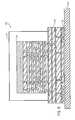
- integrated circuit die 20is shown coupled to an integrated circuit package substrate 100 , thereby forming a package 90 .
- Integrated circuit die 20is preferably attached in a flip chip configuration.
- Package substrate 100can be a plastic substrate, a PCB board substrate, a ceramic substrate, or any material for receiving die 20 .
- Package substrate 100includes a conductive layer or two or more conductive layers.
- package substrate 100includes four conductive layers: layer 102 , 104 , 106 , and 108 .
- layer 102includes contacts for receiving solder balls 64 .
- layer 102includes a conductive plane 112 electric coupleable to solder balls 64 .
- Conductive plane 112 associated with layer 102provides a bottom for the Faraday cage or shield 25 .
- Conductive plane 112preferably has an area corresponding with periphery 50 (FIG. 2) of shield 25 .
- periphery 50FIG. 2
- conductive plane 112is shown in layer 102 , any of layers 104 , 106 , or 108 can be utilized for the conductive plane.
- Package 90also includes solder balls 114 for coupling other circuitry on portion 24 (FIG. 1) of die 20 to package substrate 100 .
- Various contact and via arrangementscan be utilized to provide interconnections to substrate 100 .
- Substrate 100can also include a set of pins or solder balls 116 for coupling package substrate 100 to a printed circuit board or other module.
- Die 20can also include a cover layer (not shown) above substrate 68 .
- the cover layeris a conductive material for providing electromagnetic protection for substrate 68 of integrated circuit die 20 .
- Faraday cage or shield 25includes lateral walls 124 (indicated by cross hatching in FIG. 5 ). Side or lateral walls 124 are formed by conductive vias 62 and solder balls 64 (FIG. 3 ).
- a bottom 126 (indicated by cross hatching) of Faraday cage or shield 25can be provided by ground plane.
- the ground planecan be plane 112 of layer 102 of package substrate 100 .
- one of conductive layers 70e.g., layer 78
- an additional metal layercan be provide below layer 78 to provide the ground plane on integrated circuit die 20 .
- a ceiling or top surface 128 (indicated by cross hatching) of Faraday cage or shield 25can be provided by layer 84 (FIG. 3 ).
- a doped region within substrate 20 or a conductive layer above substrate 20can be utilized.
- a package 190 similar to package 90includes integrated circuit die 20 on a package substrate 100 .
- Package 190can include a lid 132 surrounding die 20 .
- Lid 132can be conductive and coupled to ground.
- Package substrate 100can include pins or solder balls 136 for coupling to a printed wire circuit board 134 .
- package 190can be connected as a module, such as, a multi-chip module or other device for allowing die 20 to be coupled within a system.
- lateral walls 124 associated with Faraday cage or shield 25can be comprised of a double layer of solder balls and conductive vias 150 .
- the double layeris preferably configured so that a space between vias in an interior periphery 152 is covered by vias and solder balls on an outside periphery 154 .
Landscapes
- Power Engineering (AREA)
- Engineering & Computer Science (AREA)
- Physics & Mathematics (AREA)
- Condensed Matter Physics & Semiconductors (AREA)
- General Physics & Mathematics (AREA)
- Computer Hardware Design (AREA)
- Microelectronics & Electronic Packaging (AREA)
- Health & Medical Sciences (AREA)
- Electromagnetism (AREA)
- Toxicology (AREA)
- Shielding Devices Or Components To Electric Or Magnetic Fields (AREA)
- Semiconductor Integrated Circuits (AREA)
- Internal Circuitry In Semiconductor Integrated Circuit Devices (AREA)
Abstract
Description
Claims (20)
Priority Applications (6)
| Application Number | Priority Date | Filing Date | Title |
|---|---|---|---|
| US09/785,620US6486534B1 (en) | 2001-02-16 | 2001-02-16 | Integrated circuit die having an interference shield |
| JP2002566551AJP2004521496A (en) | 2001-02-16 | 2002-02-13 | Integrated circuit die with interference shielding |
| PCT/US2002/004193WO2002067326A2 (en) | 2001-02-16 | 2002-02-13 | Integrated circuit die having an electromagnetic interference shield |
| EP02742469AEP1393372A2 (en) | 2001-02-16 | 2002-02-13 | Integrated circuit die having an interference shield |
| AU2002306475AAU2002306475A1 (en) | 2001-02-16 | 2002-02-13 | Integrated circuit die having an electromagnetic interference shield |
| US10/243,487US7151011B2 (en) | 2001-02-16 | 2002-09-13 | Integrated circuit die having an interference shield |
Applications Claiming Priority (1)
| Application Number | Priority Date | Filing Date | Title |
|---|---|---|---|
| US09/785,620US6486534B1 (en) | 2001-02-16 | 2001-02-16 | Integrated circuit die having an interference shield |
Related Child Applications (1)
| Application Number | Title | Priority Date | Filing Date |
|---|---|---|---|
| US10/243,487DivisionUS7151011B2 (en) | 2001-02-16 | 2002-09-13 | Integrated circuit die having an interference shield |
Publications (1)
| Publication Number | Publication Date |
|---|---|
| US6486534B1true US6486534B1 (en) | 2002-11-26 |
Family
ID=25136069
Family Applications (2)
| Application Number | Title | Priority Date | Filing Date |
|---|---|---|---|
| US09/785,620Expired - Fee RelatedUS6486534B1 (en) | 2001-02-16 | 2001-02-16 | Integrated circuit die having an interference shield |
| US10/243,487Expired - Fee RelatedUS7151011B2 (en) | 2001-02-16 | 2002-09-13 | Integrated circuit die having an interference shield |
Family Applications After (1)
| Application Number | Title | Priority Date | Filing Date |
|---|---|---|---|
| US10/243,487Expired - Fee RelatedUS7151011B2 (en) | 2001-02-16 | 2002-09-13 | Integrated circuit die having an interference shield |
Country Status (5)
| Country | Link |
|---|---|
| US (2) | US6486534B1 (en) |
| EP (1) | EP1393372A2 (en) |
| JP (1) | JP2004521496A (en) |
| AU (1) | AU2002306475A1 (en) |
| WO (1) | WO2002067326A2 (en) |
Cited By (39)
| Publication number | Priority date | Publication date | Assignee | Title |
|---|---|---|---|---|
| US20040178472A1 (en)* | 2002-10-15 | 2004-09-16 | Silicon Laboratories, Inc. | Electromagnetic shielding structure |
| US20040222511A1 (en)* | 2002-10-15 | 2004-11-11 | Silicon Laboratories, Inc. | Method and apparatus for electromagnetic shielding of a circuit element |
| WO2005004572A1 (en)* | 2003-07-02 | 2005-01-13 | Siemens Aktiengesellschaft | Shielding for emi-endangered electronic components and/or circuits of electronic devices |
| US20050033513A1 (en)* | 2003-08-05 | 2005-02-10 | Gasbarro Henry Frank | Dismount tablet computer assembly for wireless communication applications |
| US20050073050A1 (en)* | 2003-10-03 | 2005-04-07 | Via Technologies, Inc. | BGA package and printed circuit board for supporting the package |
| US20050098851A1 (en)* | 2002-09-27 | 2005-05-12 | Fumitaka Nakayama | Semiconductor device and manufacturing the same |
| US20050206015A1 (en)* | 2004-03-16 | 2005-09-22 | Texas Instruments Incorporated | System and method for attenuating electromagnetic interference |
| US20050212084A1 (en)* | 2003-12-11 | 2005-09-29 | Stmicroelectronics Sa | Chip circuit comprising an inductor |
| US20050253226A1 (en)* | 2001-12-08 | 2005-11-17 | Micron Technology, Inc. | Die package |
| US20050269668A1 (en)* | 2004-06-03 | 2005-12-08 | Silicon Laboratories, Inc. | Method and structure for forming relatively dense conductive layers |
| US20050274970A1 (en)* | 2004-06-14 | 2005-12-15 | Lumileds Lighting U.S., Llc | Light emitting device with transparent substrate having backside vias |
| US20060044735A1 (en)* | 2004-08-31 | 2006-03-02 | Nec Electronics Corporation | Package substrate for a semiconductor device, a fabrication method for same, and a semiconductor device |
| US20060125589A1 (en)* | 2004-12-10 | 2006-06-15 | Sharp Kabushiki Kaisha | Inductor, resonant circuit, semiconductor integrated circuit, oscillator, and communication apparatus |
| US7135766B1 (en)* | 2004-11-30 | 2006-11-14 | Rf Micro Devices, Inc. | Integrated power devices and signal isolation structure |
| US7161240B2 (en)* | 2002-06-27 | 2007-01-09 | Eastman Kodak Company | Insitu-cooled electrical assemblage |
| WO2007023327A1 (en)* | 2005-08-24 | 2007-03-01 | Infineon Technologies Ag | Magnetically alignable semiconductor chip and rewiring substrate and a method for magnetically aligning the semiconductor chip and the rewiring substrate |
| US20070052062A1 (en)* | 2005-08-23 | 2007-03-08 | International Business Machines Corporation | Vertical lc tank device |
| US20070075813A1 (en)* | 2005-09-30 | 2007-04-05 | Ligang Zhang | Self-shielding inductor |
| US7310039B1 (en) | 2001-11-30 | 2007-12-18 | Silicon Laboratories Inc. | Surface inductor |
| US20080012123A1 (en)* | 2006-07-17 | 2008-01-17 | Via Technologies, Inc. | Cooling module against esd and electronic package, assembly and system using the same |
| US20080137886A1 (en)* | 2006-10-05 | 2008-06-12 | Austsriamicrosystems Ag | Microphone arrangement and method for production thereof |
| US20090091415A1 (en)* | 2006-04-25 | 2009-04-09 | Dell Products L.P. | Solution Of Power Consumption Reduction For Inverter Covered By Metal Case |
| US20100078778A1 (en)* | 2008-09-30 | 2010-04-01 | Hans-Joachim Barth | On-Chip RF Shields with Front Side Redistribution Lines |
| US20100078779A1 (en)* | 2008-09-30 | 2010-04-01 | Hans-Joachim Barth | System on a Chip with On-Chip RF Shield |
| US20100078771A1 (en)* | 2008-09-30 | 2010-04-01 | Hans-Joachim Barth | On-Chip RF Shields with Through Substrate Conductors |
| US20100078777A1 (en)* | 2008-09-30 | 2010-04-01 | Hans-Joachim Barth | On-Chip Radio Frequency Shield with Interconnect Metallization |
| US20100315110A1 (en)* | 2009-06-10 | 2010-12-16 | Medtronic, Inc. | Hermeticity testing |
| US7936052B2 (en) | 2008-09-30 | 2011-05-03 | Infineon Technologies Ag | On-chip RF shields with backside redistribution lines |
| US20120074559A1 (en)* | 2010-09-24 | 2012-03-29 | International Business Machines Corporation | Integrated circuit package using through substrate vias to ground lid |
| US8172760B2 (en) | 2009-06-18 | 2012-05-08 | Medtronic, Inc. | Medical device encapsulated within bonded dies |
| US20120112353A1 (en)* | 2009-02-18 | 2012-05-10 | Polyic Gmbh & Co. Kg | Organic electronic circuit |
| US20120205778A1 (en)* | 2011-02-10 | 2012-08-16 | Yuan-Tai Lai | Package structure and method for manufacturing the same |
| US8424388B2 (en) | 2011-01-28 | 2013-04-23 | Medtronic, Inc. | Implantable capacitive pressure sensor apparatus and methods regarding same |
| US8502735B1 (en)* | 2009-11-18 | 2013-08-06 | Ball Aerospace & Technologies Corp. | Antenna system with integrated circuit package integrated radiators |
| US8648664B2 (en) | 2011-09-30 | 2014-02-11 | Silicon Laboratories Inc. | Mutual inductance circuits |
| US8666505B2 (en) | 2010-10-26 | 2014-03-04 | Medtronic, Inc. | Wafer-scale package including power source |
| US8889548B2 (en) | 2008-09-30 | 2014-11-18 | Infineon Technologies Ag | On-chip RF shields with backside redistribution lines |
| JP2016511939A (en)* | 2013-02-08 | 2016-04-21 | クアルコム,インコーポレイテッド | Small form factor magnetic shield for magnetoresistive random access memory (MRAM) |
| US11166642B2 (en)* | 2015-12-22 | 2021-11-09 | Kyocera Corporation | Measurement sensor package and measurement sensor |
Families Citing this family (27)
| Publication number | Priority date | Publication date | Assignee | Title |
|---|---|---|---|---|
| US6400015B1 (en)* | 2000-03-31 | 2002-06-04 | Intel Corporation | Method of creating shielded structures to protect semiconductor devices |
| US6844236B2 (en) | 2001-07-23 | 2005-01-18 | Agere Systems Inc. | Method and structure for DC and RF shielding of integrated circuits |
| JP3938742B2 (en)* | 2002-11-18 | 2007-06-27 | Necエレクトロニクス株式会社 | Electronic component device and manufacturing method thereof |
| US6836022B2 (en)* | 2003-02-13 | 2004-12-28 | Medtronic, Inc. | High voltage flip-chip component package and method for forming the same |
| DE10309614A1 (en)* | 2003-03-05 | 2004-09-23 | Infineon Technologies Ag | Semiconductor structure and production process for high frequency uses has screen between semiconductor elements passing through substrate to underside metallization |
| US7805243B2 (en)* | 2003-08-05 | 2010-09-28 | Northrop Grumman Corporation | Personal digital assistant having satellite communications capacity |
| DE102006062844B4 (en)* | 2006-05-12 | 2016-11-17 | Infineon Technologies Ag | Shielding device for shielding electromagnetic radiation |
| DE102006022360B4 (en) | 2006-05-12 | 2009-07-09 | Infineon Technologies Ag | shielding |
| US7514774B2 (en)* | 2006-09-15 | 2009-04-07 | Hong Kong Applied Science Technology Research Institute Company Limited | Stacked multi-chip package with EMI shielding |
| US8749032B2 (en)* | 2008-12-05 | 2014-06-10 | Sige Semiconductor, Inc. | Integrated circuit with improved transmission line structure and electromagnetic shielding between radio frequency circuit paths |
| TWI381306B (en) | 2009-04-23 | 2013-01-01 | Htc Corp | Portable electronic device and image data communication method thereof |
| JP6009139B2 (en)* | 2010-06-22 | 2016-10-19 | ルネサスエレクトロニクス株式会社 | Semiconductor device and manufacturing method of semiconductor device |
| US8619435B2 (en)* | 2010-07-06 | 2013-12-31 | Honeywell International Inc. | Electromagnetic interference (EMI) diverter |
| US9693492B2 (en) | 2011-04-14 | 2017-06-27 | Mitsubishi Electric Corporation | High-frequency package |
| US8948712B2 (en) | 2012-05-31 | 2015-02-03 | Skyworks Solutions, Inc. | Via density and placement in radio frequency shielding applications |
| CN104885216B (en) | 2012-07-13 | 2017-04-12 | 天工方案公司 | Racetrack design in radio frequency shielding applications |
| US9054096B2 (en) | 2012-09-25 | 2015-06-09 | Xilinx, Inc. | Noise attenuation wall |
| EP2757374A1 (en)* | 2013-01-17 | 2014-07-23 | F. Hoffmann-La Roche AG | Method for preparing an outer surface of a planar waveguide to be capable of binding target samples along a plurality of predetermined lines and a planar waveguide |
| US8748245B1 (en) | 2013-03-27 | 2014-06-10 | Io Semiconductor, Inc. | Semiconductor-on-insulator integrated circuit with interconnect below the insulator |
| US9466536B2 (en) | 2013-03-27 | 2016-10-11 | Qualcomm Incorporated | Semiconductor-on-insulator integrated circuit with back side gate |
| US9478507B2 (en) | 2013-03-27 | 2016-10-25 | Qualcomm Incorporated | Integrated circuit assembly with faraday cage |
| EP3245670B1 (en)* | 2015-01-14 | 2019-03-13 | QUALCOMM Incorporated | Integrated circuit assembly with faraday cage |
| WO2019244487A1 (en)* | 2018-06-22 | 2019-12-26 | 日本電産株式会社 | Motor |
| US11694970B2 (en) | 2021-03-19 | 2023-07-04 | Nxp B.V. | Plated pillar dies having integrated electromagnetic shield layers |
| US20230014046A1 (en)* | 2021-07-13 | 2023-01-19 | Mediatek Inc. | Semiconductor devices with in-package PGS for coupling noise suppression |
| US20240021353A1 (en)* | 2022-07-15 | 2024-01-18 | Qualcomm Incorporated | Three-dimensional vertical co-spiral inductors |
| US20250246357A1 (en)* | 2024-01-31 | 2025-07-31 | Avago Technologies International Sales Pte. Limited | Systems and methods for integrating inductors within printed circuit boards |
Citations (9)
| Publication number | Priority date | Publication date | Assignee | Title |
|---|---|---|---|---|
| US4551747A (en)* | 1982-10-05 | 1985-11-05 | Mayo Foundation | Leadless chip carrier apparatus providing for a transmission line environment and improved heat dissipation |
| US5446311A (en)* | 1994-09-16 | 1995-08-29 | International Business Machines Corporation | High-Q inductors in silicon technology without expensive metalization |
| US5592391A (en)* | 1993-03-05 | 1997-01-07 | International Business Machines Corporation | Faraday cage for a printed circuit card |
| JPH10112517A (en)* | 1996-10-03 | 1998-04-28 | Ngk Spark Plug Co Ltd | Electronic components housing package |
| US5955789A (en) | 1997-04-16 | 1999-09-21 | International Business Machines Corporation | Ball grid array module |
| US5986340A (en) | 1996-05-02 | 1999-11-16 | National Semiconductor Corporation | Ball grid array package with enhanced thermal and electrical characteristics and electronic device incorporating same |
| US6166403A (en)* | 1997-11-12 | 2000-12-26 | Lsi Logic Corporation | Integrated circuit having embedded memory with electromagnetic shield |
| US6181279B1 (en)* | 1998-05-08 | 2001-01-30 | Northrop Grumman Corporation | Patch antenna with an electrically small ground plate using peripheral parasitic stubs |
| US6229404B1 (en)* | 1998-08-31 | 2001-05-08 | Kyocera Corporation | Crystal oscillator |
Family Cites Families (3)
| Publication number | Priority date | Publication date | Assignee | Title |
|---|---|---|---|---|
| US5256590A (en)* | 1989-11-24 | 1993-10-26 | Mitsubishi Denki Kabushiki Kaisha | Method of making a shielded semiconductor device |
| WO1997035344A1 (en)* | 1996-03-22 | 1997-09-25 | Telefonaktiebolaget Lm Ericsson | Semiconductor device shielded by an array of electrically conducting pins and a method to manufacture such a device |
| US6130483A (en)* | 1997-03-05 | 2000-10-10 | Kabushiki Kaisha Toshiba | MMIC module using flip-chip mounting |
- 2001
- 2001-02-16USUS09/785,620patent/US6486534B1/ennot_activeExpired - Fee Related
- 2002
- 2002-02-13AUAU2002306475Apatent/AU2002306475A1/ennot_activeAbandoned
- 2002-02-13EPEP02742469Apatent/EP1393372A2/ennot_activeWithdrawn
- 2002-02-13JPJP2002566551Apatent/JP2004521496A/enactivePending
- 2002-02-13WOPCT/US2002/004193patent/WO2002067326A2/enactiveApplication Filing
- 2002-09-13USUS10/243,487patent/US7151011B2/ennot_activeExpired - Fee Related
Patent Citations (9)
| Publication number | Priority date | Publication date | Assignee | Title |
|---|---|---|---|---|
| US4551747A (en)* | 1982-10-05 | 1985-11-05 | Mayo Foundation | Leadless chip carrier apparatus providing for a transmission line environment and improved heat dissipation |
| US5592391A (en)* | 1993-03-05 | 1997-01-07 | International Business Machines Corporation | Faraday cage for a printed circuit card |
| US5446311A (en)* | 1994-09-16 | 1995-08-29 | International Business Machines Corporation | High-Q inductors in silicon technology without expensive metalization |
| US5986340A (en) | 1996-05-02 | 1999-11-16 | National Semiconductor Corporation | Ball grid array package with enhanced thermal and electrical characteristics and electronic device incorporating same |
| JPH10112517A (en)* | 1996-10-03 | 1998-04-28 | Ngk Spark Plug Co Ltd | Electronic components housing package |
| US5955789A (en) | 1997-04-16 | 1999-09-21 | International Business Machines Corporation | Ball grid array module |
| US6166403A (en)* | 1997-11-12 | 2000-12-26 | Lsi Logic Corporation | Integrated circuit having embedded memory with electromagnetic shield |
| US6181279B1 (en)* | 1998-05-08 | 2001-01-30 | Northrop Grumman Corporation | Patch antenna with an electrically small ground plate using peripheral parasitic stubs |
| US6229404B1 (en)* | 1998-08-31 | 2001-05-08 | Kyocera Corporation | Crystal oscillator |
Cited By (96)
| Publication number | Priority date | Publication date | Assignee | Title |
|---|---|---|---|---|
| US7310039B1 (en) | 2001-11-30 | 2007-12-18 | Silicon Laboratories Inc. | Surface inductor |
| US20050253226A1 (en)* | 2001-12-08 | 2005-11-17 | Micron Technology, Inc. | Die package |
| US7489028B2 (en)* | 2001-12-08 | 2009-02-10 | Micron Technology, Inc. | Die package |
| US7161240B2 (en)* | 2002-06-27 | 2007-01-09 | Eastman Kodak Company | Insitu-cooled electrical assemblage |
| US20110127594A1 (en)* | 2002-09-27 | 2011-06-02 | Fumitaka Nakayama | Semiconductor device and manufacturing the same |
| US20060261442A1 (en)* | 2002-09-27 | 2006-11-23 | Fumitaka Nakayama | Semiconductor device and manufacturing the same |
| US20050098851A1 (en)* | 2002-09-27 | 2005-05-12 | Fumitaka Nakayama | Semiconductor device and manufacturing the same |
| US7479681B2 (en) | 2002-09-27 | 2009-01-20 | Renesas Eastern Technology Corp. | Multilayered semiconductor structure containing a MISFET, a resistor, a capacitor, and an inductor |
| US20090108371A1 (en)* | 2002-09-27 | 2009-04-30 | Fumitaka Nakayama | Semiconductor device and manufacturing the same |
| US7671381B2 (en) | 2002-09-27 | 2010-03-02 | Renesas Eastern Japan Semiconductor, Inc. | Semiconductor device and manufacturing the same |
| US20070194407A1 (en)* | 2002-09-27 | 2007-08-23 | Fumitaka Nakayama | Semiconductor device and manufacturing the same |
| US7217987B2 (en) | 2002-09-27 | 2007-05-15 | Renesas Technology Corp. | Semiconductor device and manufacturing the same |
| US20100097157A1 (en)* | 2002-09-27 | 2010-04-22 | Fumitaka Nakayama | Semiconductor device and manufacturing the same |
| US7741656B2 (en) | 2002-09-27 | 2010-06-22 | Renesas Technology Corporation | Semiconductor device and manufacturing the same |
| US8080831B2 (en) | 2002-09-27 | 2011-12-20 | Renesas Electronics Corporation | Semiconductor device and manufacturing the same |
| US7087977B2 (en)* | 2002-09-27 | 2006-08-08 | Renesas Technology Corp. | Semiconductor device including multiple wiring layers and circuits operating in different frequency bands |
| US20040178472A1 (en)* | 2002-10-15 | 2004-09-16 | Silicon Laboratories, Inc. | Electromagnetic shielding structure |
| US20040222506A1 (en)* | 2002-10-15 | 2004-11-11 | Silicon Laboratories, Inc. | Integrated circuit package configuration incorporating shielded circuit element structure |
| US7141883B2 (en) | 2002-10-15 | 2006-11-28 | Silicon Laboratories Inc. | Integrated circuit package configuration incorporating shielded circuit element structure |
| US7498656B2 (en) | 2002-10-15 | 2009-03-03 | Silicon Laboratories Inc. | Electromagnetic shielding structure |
| US20040222511A1 (en)* | 2002-10-15 | 2004-11-11 | Silicon Laboratories, Inc. | Method and apparatus for electromagnetic shielding of a circuit element |
| US20060027913A1 (en)* | 2003-07-02 | 2006-02-09 | Matthias Lungwitz | Shielding for emi-sensitive electronic components and or circuits of electronic devices |
| WO2005004572A1 (en)* | 2003-07-02 | 2005-01-13 | Siemens Aktiengesellschaft | Shielding for emi-endangered electronic components and/or circuits of electronic devices |
| KR100851683B1 (en) | 2003-07-02 | 2008-08-11 | 지멘스 악티엔게젤샤프트 | Shielding electronic components and / or circuits of electronic devices disturbed by electromagnetic interference |
| CN100386010C (en)* | 2003-07-02 | 2008-04-30 | 西门子公司 | Shielding of electronic components and/or circuits of electronic devices susceptible to electromagnetic interference |
| US7269032B2 (en) | 2003-07-02 | 2007-09-11 | Siemens Aktiengesellschaft | Shielding for EMI-sensitive electronic components and or circuits of electronic devices |
| US20050033513A1 (en)* | 2003-08-05 | 2005-02-10 | Gasbarro Henry Frank | Dismount tablet computer assembly for wireless communication applications |
| US7813876B2 (en)* | 2003-08-05 | 2010-10-12 | Northrop Grumman Corporation | Dismount tablet computer assembly for wireless communication applications |
| US20050073050A1 (en)* | 2003-10-03 | 2005-04-07 | Via Technologies, Inc. | BGA package and printed circuit board for supporting the package |
| EP1553812A3 (en)* | 2003-12-11 | 2013-04-03 | STMicroelectronics S.A. | Semiconductor chip and circuit including a shielded inductance |
| US20050212084A1 (en)* | 2003-12-11 | 2005-09-29 | Stmicroelectronics Sa | Chip circuit comprising an inductor |
| US7233055B2 (en)* | 2003-12-11 | 2007-06-19 | Stmicroelectronics Sa | Chip circuit comprising an inductor |
| US20050206015A1 (en)* | 2004-03-16 | 2005-09-22 | Texas Instruments Incorporated | System and method for attenuating electromagnetic interference |
| US20050269668A1 (en)* | 2004-06-03 | 2005-12-08 | Silicon Laboratories, Inc. | Method and structure for forming relatively dense conductive layers |
| US7375411B2 (en) | 2004-06-03 | 2008-05-20 | Silicon Laboratories Inc. | Method and structure for forming relatively dense conductive layers |
| US20050274970A1 (en)* | 2004-06-14 | 2005-12-15 | Lumileds Lighting U.S., Llc | Light emitting device with transparent substrate having backside vias |
| US20060044735A1 (en)* | 2004-08-31 | 2006-03-02 | Nec Electronics Corporation | Package substrate for a semiconductor device, a fabrication method for same, and a semiconductor device |
| US7378745B2 (en)* | 2004-08-31 | 2008-05-27 | Nec Electronics Corporation | Package substrate for a semiconductor device having thermoplastic resin layers and conductive patterns |
| US7135766B1 (en)* | 2004-11-30 | 2006-11-14 | Rf Micro Devices, Inc. | Integrated power devices and signal isolation structure |
| US7295096B2 (en)* | 2004-12-10 | 2007-11-13 | Sharp Kabushiki Kaisha | Inductor, resonant circuit, semiconductor integrated circuit, oscillator, and communication apparatus |
| US20060125589A1 (en)* | 2004-12-10 | 2006-06-15 | Sharp Kabushiki Kaisha | Inductor, resonant circuit, semiconductor integrated circuit, oscillator, and communication apparatus |
| US20070052062A1 (en)* | 2005-08-23 | 2007-03-08 | International Business Machines Corporation | Vertical lc tank device |
| US20080012091A1 (en)* | 2005-08-23 | 2008-01-17 | Hanyi Ding | Vertical lc tank device |
| US7564319B2 (en) | 2005-08-23 | 2009-07-21 | International Business Machines Corporation | Vertical LC tank device |
| US7323948B2 (en)* | 2005-08-23 | 2008-01-29 | International Business Machines Corporation | Vertical LC tank device |
| US7994608B2 (en) | 2005-08-24 | 2011-08-09 | Infineon Technologies Ag | Magnetically alignable integrated circuit device |
| WO2007023327A1 (en)* | 2005-08-24 | 2007-03-01 | Infineon Technologies Ag | Magnetically alignable semiconductor chip and rewiring substrate and a method for magnetically aligning the semiconductor chip and the rewiring substrate |
| US20080265367A1 (en)* | 2005-08-24 | 2008-10-30 | Infineon Technologies Ag | Magnetically Alignable Integrated Circuit Device |
| US20070075813A1 (en)* | 2005-09-30 | 2007-04-05 | Ligang Zhang | Self-shielding inductor |
| US7501924B2 (en) | 2005-09-30 | 2009-03-10 | Silicon Laboratories Inc. | Self-shielding inductor |
| US20090091415A1 (en)* | 2006-04-25 | 2009-04-09 | Dell Products L.P. | Solution Of Power Consumption Reduction For Inverter Covered By Metal Case |
| US8080864B2 (en)* | 2006-04-25 | 2011-12-20 | Dell Products L.P. | Solution of power consumption reduction for inverter covered by metal case |
| US20080012123A1 (en)* | 2006-07-17 | 2008-01-17 | Via Technologies, Inc. | Cooling module against esd and electronic package, assembly and system using the same |
| US7560812B2 (en) | 2006-07-17 | 2009-07-14 | Via Technologies, Inc. | Cooling module against ESD and electronic package, assembly and system using the same |
| DE102006047203B4 (en)* | 2006-10-05 | 2013-01-31 | Austriamicrosystems Ag | Microphone arrangement and method for its production |
| US8199963B2 (en) | 2006-10-05 | 2012-06-12 | Austriamicrosystems Ag | Microphone arrangement and method for production thereof |
| US20080137886A1 (en)* | 2006-10-05 | 2008-06-12 | Austsriamicrosystems Ag | Microphone arrangement and method for production thereof |
| US20100078779A1 (en)* | 2008-09-30 | 2010-04-01 | Hans-Joachim Barth | System on a Chip with On-Chip RF Shield |
| US8748287B2 (en) | 2008-09-30 | 2014-06-10 | Infineon Technologies Ag | System on a chip with on-chip RF shield |
| US7948064B2 (en) | 2008-09-30 | 2011-05-24 | Infineon Technologies Ag | System on a chip with on-chip RF shield |
| DE102009061243B3 (en) | 2008-09-30 | 2018-07-12 | Infineon Technologies Ag | System on a chip with RF shielding on the chip |
| DE102009044967B4 (en) | 2008-09-30 | 2018-06-21 | Infineon Technologies Ag | System on a chip with RF shielding on the chip |
| US20110201175A1 (en)* | 2008-09-30 | 2011-08-18 | Hans-Joachim Barth | System on a Chip with On-Chip RF Shield |
| US8063469B2 (en) | 2008-09-30 | 2011-11-22 | Infineon Technologies Ag | On-chip radio frequency shield with interconnect metallization |
| US9390973B2 (en) | 2008-09-30 | 2016-07-12 | Infineon Technologies Ag | On-chip RF shields with backside redistribution lines |
| US8889548B2 (en) | 2008-09-30 | 2014-11-18 | Infineon Technologies Ag | On-chip RF shields with backside redistribution lines |
| US20100078771A1 (en)* | 2008-09-30 | 2010-04-01 | Hans-Joachim Barth | On-Chip RF Shields with Through Substrate Conductors |
| US7936052B2 (en) | 2008-09-30 | 2011-05-03 | Infineon Technologies Ag | On-chip RF shields with backside redistribution lines |
| US8617929B2 (en) | 2008-09-30 | 2013-12-31 | Infineon Technologies Ag | On-Chip RF shields with front side redistribution lines |
| US8169059B2 (en) | 2008-09-30 | 2012-05-01 | Infineon Technologies Ag | On-chip RF shields with through substrate conductors |
| US8536683B2 (en) | 2008-09-30 | 2013-09-17 | Infineon Technologies Ag | System on a chip with on-chip RF shield |
| US20100078778A1 (en)* | 2008-09-30 | 2010-04-01 | Hans-Joachim Barth | On-Chip RF Shields with Front Side Redistribution Lines |
| US8178953B2 (en) | 2008-09-30 | 2012-05-15 | Infineon Technologies Ag | On-chip RF shields with front side redistribution lines |
| US20100078777A1 (en)* | 2008-09-30 | 2010-04-01 | Hans-Joachim Barth | On-Chip Radio Frequency Shield with Interconnect Metallization |
| US8450731B2 (en)* | 2009-02-18 | 2013-05-28 | Polyic Gmbh & Co. Kg | Organic electronic circuit |
| US20120112353A1 (en)* | 2009-02-18 | 2012-05-10 | Polyic Gmbh & Co. Kg | Organic electronic circuit |
| US8125058B2 (en) | 2009-06-10 | 2012-02-28 | Medtronic, Inc. | Faraday cage for circuitry using substrates |
| US20100314733A1 (en)* | 2009-06-10 | 2010-12-16 | Medtronic, Inc. | Apparatus for restricting moisture ingress |
| US8263436B2 (en) | 2009-06-10 | 2012-09-11 | Medtronic, Inc. | Apparatus for restricting moisture ingress |
| US7902851B2 (en) | 2009-06-10 | 2011-03-08 | Medtronic, Inc. | Hermeticity testing |
| US20100314726A1 (en)* | 2009-06-10 | 2010-12-16 | Medtronic, Inc. | Faraday cage for circuitry using substrates |
| US8072056B2 (en) | 2009-06-10 | 2011-12-06 | Medtronic, Inc. | Apparatus for restricting moisture ingress |
| US8389331B2 (en) | 2009-06-10 | 2013-03-05 | Medtronic, Inc. | Apparatus for restricting moisture ingress |
| US20100315110A1 (en)* | 2009-06-10 | 2010-12-16 | Medtronic, Inc. | Hermeticity testing |
| US8172760B2 (en) | 2009-06-18 | 2012-05-08 | Medtronic, Inc. | Medical device encapsulated within bonded dies |
| US8502735B1 (en)* | 2009-11-18 | 2013-08-06 | Ball Aerospace & Technologies Corp. | Antenna system with integrated circuit package integrated radiators |
| US20120074559A1 (en)* | 2010-09-24 | 2012-03-29 | International Business Machines Corporation | Integrated circuit package using through substrate vias to ground lid |
| US8666505B2 (en) | 2010-10-26 | 2014-03-04 | Medtronic, Inc. | Wafer-scale package including power source |
| US9318400B2 (en) | 2010-10-26 | 2016-04-19 | Medtronic, Inc. | Wafer-scale package including power source |
| US9431312B2 (en) | 2010-10-26 | 2016-08-30 | Medtronic, Inc. | Wafer-scale package including power source |
| US8424388B2 (en) | 2011-01-28 | 2013-04-23 | Medtronic, Inc. | Implantable capacitive pressure sensor apparatus and methods regarding same |
| US20120205778A1 (en)* | 2011-02-10 | 2012-08-16 | Yuan-Tai Lai | Package structure and method for manufacturing the same |
| US8648664B2 (en) | 2011-09-30 | 2014-02-11 | Silicon Laboratories Inc. | Mutual inductance circuits |
| JP2016511939A (en)* | 2013-02-08 | 2016-04-21 | クアルコム,インコーポレイテッド | Small form factor magnetic shield for magnetoresistive random access memory (MRAM) |
| KR20160108598A (en)* | 2013-02-08 | 2016-09-19 | 퀄컴 인코포레이티드 | Small form factor magnetic shield for magnetorestrictive random access memory (mram) |
| US11166642B2 (en)* | 2015-12-22 | 2021-11-09 | Kyocera Corporation | Measurement sensor package and measurement sensor |
Also Published As
| Publication number | Publication date |
|---|---|
| WO2002067326A3 (en) | 2003-12-18 |
| WO2002067326A9 (en) | 2004-04-01 |
| EP1393372A2 (en) | 2004-03-03 |
| AU2002306475A1 (en) | 2002-09-04 |
| WO2002067326A2 (en) | 2002-08-29 |
| US7151011B2 (en) | 2006-12-19 |
| US20030017646A1 (en) | 2003-01-23 |
| JP2004521496A (en) | 2004-07-15 |
Similar Documents
| Publication | Publication Date | Title |
|---|---|---|
| US6486534B1 (en) | Integrated circuit die having an interference shield | |
| JP2968253B2 (en) | Ball grid array module | |
| US6507115B2 (en) | Multi-chip integrated circuit module | |
| US6734539B2 (en) | Stacked module package | |
| US6747362B2 (en) | Perimeter matrix ball grid array circuit package with a populated center | |
| US6222246B1 (en) | Flip-chip having an on-chip decoupling capacitor | |
| US6515870B1 (en) | Package integrated faraday cage to reduce electromagnetic emissions from an integrated circuit | |
| US6184580B1 (en) | Ball grid array package with conductive leads | |
| US5175613A (en) | Package for EMI, ESD, thermal, and mechanical shock protection of circuit chips | |
| US7088009B2 (en) | Wirebonded assemblage method and apparatus | |
| US6011299A (en) | Apparatus to minimize integrated circuit heatsink E.M.I. radiation | |
| TWI506707B (en) | Integrated circuit packaging system with leadframe interposer and method of manufacture thereof | |
| EP0340959A2 (en) | Package for EMI, ESD, thermal, and mechanical shock protection of circuit chips | |
| WO2005067045A1 (en) | Array capacitors with voids to enable a full-grid socket | |
| US20120074559A1 (en) | Integrated circuit package using through substrate vias to ground lid | |
| US11810915B2 (en) | Semiconductor package with redistribution substrate having embedded passive device | |
| US6924562B2 (en) | Semiconductor integrated circuit having at least one of a power supply plane and ground plane divided into parts insulated from one another | |
| US20080036049A1 (en) | Stacked integration module and method for manufacturing the same | |
| US20230051507A1 (en) | Semiconductor device package with semiconductive thermal pedestal | |
| KR101305581B1 (en) | Shield member and pcb comprising the shield member | |
| US6256189B1 (en) | Heat slug design which facilitates mounting of discrete components on a package without losing lands or pins in the package | |
| CN118116895A (en) | Electronic device package EMI shielding using grounding die interconnects | |
| US20030107116A1 (en) | Windowframe capacitor | |
| KR20180029404A (en) | Semi-conductor package | |
| WO2001080314A2 (en) | Performance enhanced leaded packaging for electrical components |
Legal Events
| Date | Code | Title | Description |
|---|---|---|---|
| AS | Assignment | Owner name:ASHVATTHA SEMICONDUCTOR, INC., FLORIDA Free format text:ASSIGNMENT OF ASSIGNORS INTEREST;ASSIGNORS:SRIDHARAN, GURUSWAMI M.;SRIDHARAN, KARTIK M.;REEL/FRAME:011568/0321 Effective date:20010215 | |
| CC | Certificate of correction | ||
| AS | Assignment | Owner name:COMSTELLAR TECHNOLOGIES, INC., CALIFORNIA Free format text:SECURITY INTEREST;ASSIGNOR:ASHVATTHA SEMICONDUCTOR, INC.;REEL/FRAME:013735/0458 Effective date:20030611 Owner name:CROSSBOW VENTURE PARTNERS, L.P., FLORIDA Free format text:SECURITY INTEREST;ASSIGNOR:ASHVATTHA SEMICONDUCTOR, INC.;REEL/FRAME:013735/0061 Effective date:20030611 | |
| AS | Assignment | Owner name:CROSSBOW EQUITY PARTNERS, L.P., FLORIDA Free format text:SECURITY INTEREST;ASSIGNOR:ASHVATTHA SEMICONDUCTOR;REEL/FRAME:014384/0067 Effective date:20030813 Owner name:REDWOOD VENTURES III, L.P., CALIFORNIA Free format text:SECURITY INTEREST;ASSIGNOR:ASHVATTHA SEMICONDUCTOR;REEL/FRAME:014384/0060 Effective date:20030813 | |
| AS | Assignment | Owner name:ASHVATTHA SEMICONDUCTOR, INC., CALIFORNIA Free format text:TERMINATION OF SECURITY AGREEMENT;ASSIGNOR:COMSTELLAR TECHNOLOGIES, INC.;REEL/FRAME:015861/0827 Effective date:20040330 Owner name:ASHVATTHA SEMICONDUCTOR, INC., CALIFORNIA Free format text:TERMINATION OF SECURITY AGREEMENT;ASSIGNOR:CROSSBOW VENTURE PARTNERS, L.P.;REEL/FRAME:015886/0709 Effective date:20040330 Owner name:ASHVATTHA SEMICONDUCTOR, INC., CALIFORNIA Free format text:TERMINATION OF SECURITY AGREEMENT;ASSIGNOR:REDWOOD VENTURES III, L.P.;REEL/FRAME:015201/0090 Effective date:20040330 | |
| AS | Assignment | Owner name:CROSSBOW EQUITY PARTNERS, L.P., FLORIDA Free format text:SECURITY AGREEMENT;ASSIGNOR:ASHVATTHA SEMICONDUCTOR, INC.;REEL/FRAME:015201/0149 Effective date:20040330 | |
| AS | Assignment | Owner name:SPECTRA WIRELESS, INC., CALIFORNIA Free format text:CHANGE OF NAME;ASSIGNOR:ASHVATTA SEMICONDUCTER INC;REEL/FRAME:015756/0352 Effective date:20050304 | |
| FPAY | Fee payment | Year of fee payment:4 | |
| AS | Assignment | Owner name:INSILICA, INC., CALIFORNIA Free format text:ASSIGNMENT OF ASSIGNORS INTEREST;ASSIGNOR:SPECTRA WIRELESS INC.;REEL/FRAME:019019/0494 Effective date:20050812 | |
| FPAY | Fee payment | Year of fee payment:8 | |
| REMI | Maintenance fee reminder mailed | ||
| LAPS | Lapse for failure to pay maintenance fees | ||
| STCH | Information on status: patent discontinuation | Free format text:PATENT EXPIRED DUE TO NONPAYMENT OF MAINTENANCE FEES UNDER 37 CFR 1.362 | |
| FP | Lapsed due to failure to pay maintenance fee | Effective date:20141126 |