US6486068B2 - Method for manufacturing group III nitride compound semiconductor laser diodes - Google Patents
Method for manufacturing group III nitride compound semiconductor laser diodesDownload PDFInfo
- Publication number
- US6486068B2 US6486068B2US09/004,608US460898AUS6486068B2US 6486068 B2US6486068 B2US 6486068B2US 460898 AUS460898 AUS 460898AUS 6486068 B2US6486068 B2US 6486068B2
- Authority
- US
- United States
- Prior art keywords
- facets
- etching
- layer
- ion beam
- forming
- Prior art date
- Legal status (The legal status is an assumption and is not a legal conclusion. Google has not performed a legal analysis and makes no representation as to the accuracy of the status listed.)
- Expired - Fee Related
Links
Images


Classifications
- H—ELECTRICITY
- H01—ELECTRIC ELEMENTS
- H01S—DEVICES USING THE PROCESS OF LIGHT AMPLIFICATION BY STIMULATED EMISSION OF RADIATION [LASER] TO AMPLIFY OR GENERATE LIGHT; DEVICES USING STIMULATED EMISSION OF ELECTROMAGNETIC RADIATION IN WAVE RANGES OTHER THAN OPTICAL
- H01S5/00—Semiconductor lasers
- H01S5/02—Structural details or components not essential to laser action
- H01S5/0201—Separation of the wafer into individual elements, e.g. by dicing, cleaving, etching or directly during growth
- H01S5/0203—Etching
- H—ELECTRICITY
- H01—ELECTRIC ELEMENTS
- H01S—DEVICES USING THE PROCESS OF LIGHT AMPLIFICATION BY STIMULATED EMISSION OF RADIATION [LASER] TO AMPLIFY OR GENERATE LIGHT; DEVICES USING STIMULATED EMISSION OF ELECTROMAGNETIC RADIATION IN WAVE RANGES OTHER THAN OPTICAL
- H01S5/00—Semiconductor lasers
- H01S5/30—Structure or shape of the active region; Materials used for the active region
- H01S5/32—Structure or shape of the active region; Materials used for the active region comprising PN junctions, e.g. hetero- or double- heterostructures
- H01S5/323—Structure or shape of the active region; Materials used for the active region comprising PN junctions, e.g. hetero- or double- heterostructures in AIIIBV compounds, e.g. AlGaAs-laser, InP-based laser
- H01S5/32308—Structure or shape of the active region; Materials used for the active region comprising PN junctions, e.g. hetero- or double- heterostructures in AIIIBV compounds, e.g. AlGaAs-laser, InP-based laser emitting light at a wavelength less than 900 nm
- H01S5/32341—Structure or shape of the active region; Materials used for the active region comprising PN junctions, e.g. hetero- or double- heterostructures in AIIIBV compounds, e.g. AlGaAs-laser, InP-based laser emitting light at a wavelength less than 900 nm blue laser based on GaN or GaP
Definitions
- the present inventionrelates to a method for manufacturing a group III nitride compound semiconductor laser diode (hereinafter “LD”).
- LDgroup III nitride compound semiconductor laser diode
- the present inventionrelates to a method for manufacturing a facet of a cavity of an LD.
- a light-emitting diode (LED) and a laser diode (LD) which emit blue lighthave been known, which comprise layers of gallium nitride group compound semiconductor (AlGaInN) formed on a sapphire substrate.
- AlGaInNgallium nitride group compound semiconductor
- a verticality and a parallelism of one pair of opposite facets of a cavityshould be kept high to reflect and oscillate lights of an LD effectively.
- a cleavageis the best way to form one pair of opposite facets which has high verticality and parallelism, it is difficult to cleave the facets of the LD because the substrate and the layers are made of different materials. Accordingly, dry etching is used to form the facets as an alternative method of the cleavage.
- the facets of the cavity formed by dry etchingis damaged by ion and has a magnitude of surface roughness of 200 ⁇ .
- an optical reflectiveness of the facetsis lowered and the oscillation threshold current density is heightened.
- the filmscannot be formed accurately as designed because the facets of the cavity are rough. As a result, lights are scattered on the facets and the efficiency of confining emitted lights in an active layer is lowered.
- the present inventionis related to a method for manufacturing a laser diode using Group III nitride compound semiconductor comprising the steps of forming layers comprising Group III nitride compound semiconductor on a substrate, dry-etching each of said layers to form one pair of opposite facets of a cavity, and further etching said dry-etched facets by gas cluster ion beam etching.
- the surface roughness of the facets of the cavity by dry etchingis reduced by gas cluster ion beam etching, a mirror reflection of the facets is improved, the effect of confining lights between the opposite facets is increased, and an oscillation threshold current density of the LD is lowered.
- a Group III nitride compound semiconductorshould be preferably a material satisfies the formula Al x Ga y In 1 ⁇ x ⁇ y N(0 ⁇ x ⁇ 1, 0 ⁇ y ⁇ 1, 0 ⁇ x+y ⁇ 1) to obtain blue color short wave LD.
- the semiconductoris formed by a cladding layer of Ga x1 In 1 ⁇ x1 N (0 ⁇ x 1 ⁇ 1) and an active layer of Ga x2 In 1 ⁇ x2 N(0 ⁇ x 2 ⁇ 1), output power of the blue color LD is improved.
- the facetsare effectively formed by reactive ion beam etching (RIBE hereinafter) more than by dry etching. It is more preferable to use RIBE with Cl 2 gas, because a higher etching rate can be obtained.
- a rough layer on the facets formed by dry etchingis removed effectively by gas cluster ion beam etching, and a mirror reflection of the facets is improved.
- the mirror reflection of the facetsis improved to form the facets by gas cluster ion beam etching using inert gases like argon (Ar), helium (He), neon (Ne), krypton (Kr), xenon (Xe), radon (Rn), nitrogen (N 2 ), and carbon dioxide (CO 2 ) or reactive gases like hydrogen chloride (HCl), chlorine (Cl 2 ), carbon chloride trifluoride (CClF 3 ), bromine (Br), and hydrogen bromide (HBr).
- inert gaseslike argon (Ar), helium (He), neon (Ne), krypton (Kr), xenon (Xe), radon (Rn), nitrogen (N 2 ), and carbon dioxide (CO 2 ) or reactive gases like hydrogen chloride (HCl), chlorine (Cl 2 ),
- a wafer treated by above-mentioned processis divided into peaces of strip parallel to the facets of the cavity.
- Each of the stripsare disposed with the facets of the cavity facing upside, and the facet is etched by cluster beam etching to improve the efficiency of a mirror reflection of the facet.
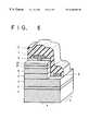
- FIG. 1is a constitutive view illustrating the structure of a laser diode in the example set forth below;
- FIGS. 2 to 5are sectional views illustrating successive steps of manufacturing the LD
- FIG. 6is a perspective-sectional view illustrating a successive steps of manufacturing the LD
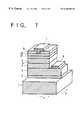
- FIG. 7is a perspective-sectional view illustrating the structure of the LD.
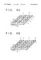
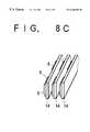
- FIG. 8is a view illustrating methods of cutting a wafer and a cluster beam etching.
- FIG. 1shows a whole structure of an LD 100 in this embodiment.
- the LD 100has a sapphire substrate 1 on which about 500 ⁇ in thickness of aluminum nitride (AlN) buffer layer 2 is formed.
- Five semiconductor layersare consecutively formed on the buffer layer 2 : about 2.2 ⁇ m in thickness of silicon (Si) doped gallium nitride (GaN) layer 3 of high carrier concentration (n + -type), having an electron concentration of 2 ⁇ 10 18 /cm 3 and Si concentration of 4 ⁇ 10 18 /cm 3 ; about 1.0 ⁇ m in thickness of Si-doped n-Al 0.08 Ga 0.92 N cladding layer 4 of n-type, having an electron concentration of 2 ⁇ 10 18 /cm 3 and Si concentration of 4 ⁇ 10 18 /cm 3 ; about 0.05 ⁇ m in thickness of Ga 0.92 In 0.08 N active layer 5 ; about 1.0 ⁇ m in thickness of Mg-doped Al 0.08 Ga 0.92 N cladding
- An insulating film of SiO 2 layer 9is formed on the contact layer 62 and has a window through which electrode layer 7 including Ni was formed in contact with the contact layer 62 .
- An Ni electrode layer 8is formed on some portion of the n + layer 3 of high carrier concentration.
- MOVPEmetal organic vapor phase deposition
- the gases employed in this processwere ammonia (NH 3 ), a carrier gas (H 2 or N 2 ), trimethyl gallium (Ga(CH 3 ) 3 ) (hereinafter TMG), trimethyl aluminum (Al(CH 3 ) 3 ) (hereinafter TMA), trimethyl indium (In(CH 3 ) 3 ) (hereinafter TMI), silane (SiH 4 ), and biscyclopentadienyl magnesium (Mg(C 5 H 5 ) 2 ) (hereinafter CP 2 Mg).
- the single crystalline sapphire substrate 1was placed on a susceptor in a reaction chamber for the MOVPE treatment after its main surface ‘a’ was cleaned by an organic washing solvent and heat treatment. Then the sapphire substrate 1 was gaseous phase etched at 1100° C. by H 2 vapor fed into the chamber at a flow rate of 2 liter/min. under normal pressure.
- AlN buffer layer 2About 500 ⁇ in thickness of AlN buffer layer 2 was formed on the surface ‘a’ of the baked sapphire substrate 1 under conditions controlled by lowering the temperature in the chamber to 400° C., keeping the temperature constant, and concurrently supplying H 2 at a flow rate of 20 liter/min., NH 3 at 10 liter/min., and TMA at 1.8 ⁇ 10 ⁇ 5 mol/min.
- Si-doped GaNwas formed on the buffer layer 2 , as an n + layer 3 of high carrier concentration with an Si concentration of about 4 ⁇ 10 18 /cm 3 and an electron concentration of about 2 ⁇ 10 18 /cm 3 , under conditions controlled by keeping the temperature of the sapphire substrate 1 at 1150° C. and concurrently supplying for 30 min. H 2 at a flow rate of 20 liter/min., NH 3 at 10 liter/min., TMG at 1.7 ⁇ 10 ⁇ 4 mol/min., and silane diluted to 0.86 ppm by H 2 at 200 ml/min.
- n + layer 3about 1.0 ⁇ m in thickness of Si-doped Al 0.08 Ga 0.92 N was formed on the n + layer 3 , as a cladding layer 4 of n-type with an electron concentration of about 2 ⁇ 10 18 /cm 3 and Si concentration of about 4 ⁇ 10 18 /cm 3 , under conditions controlled by keeping the temperature of the sapphire substrate 1 at 1100° C. and concurrently supplying for 60 min. N 2 or H 2 at a flow rate of 10 liter/min., NH 3 at 10 liter/min., TMG at 1.12 ⁇ 10 ⁇ 4 mol/min., TMA at 0.47 ⁇ 10 ⁇ 4 mol/min., and silane diluted to 0.86 ppm by H 2 at 10 ⁇ 10 ⁇ 9 mol/min.
- Ga 0.92 In 0.08 Nwas formed on the cladding layer 4 as an active layer 5 under conditions controlled by keeping the temperature of the sapphire substrate 1 at 850° C. and concurrently supplying for 6 min. N 2 or H 2 at a flow rate of 20 liter/min., NH 3 at 10 liter/min., TMG at 1.53 ⁇ 10 ⁇ 4 mol/min., and TMI at 0.02 ⁇ 10 31 4 mol/min.
- Mg-doped Al 0.08 Ga 0.92 N of p-typeserving as a cladding layer 61 with an Mg concentration of about 1 ⁇ 10 20 /cm 3
- the active layer 5under conditions controlled by keeping the temperature of the sapphire substrate 1 at 1100° C. and concurrently supplying for 60 min. N 2 or H 2 at a flow rate of 20 liter/min., NH 3 at 10 liter/min., TMG at 1.12 ⁇ 10 ⁇ 4 mol/min., TMA at 0.47 ⁇ 10 ⁇ 4 mol/min., and CP 2 Mg at 2 ⁇ 10 ⁇ 4 mol/min.
- the resistivity of the cladding layer 61was 10 8 ⁇ cm or more, exhibiting insulating characteristics.
- Mg-doped GaNserving as a contact layer 62
- a contact layer 62was formed on the cladding layer 61 with an Mg concentration of 2 ⁇ 10 20 /cm 3 under conditions controlled by keeping the temperature of the sapphire substrate 1 at 1100° C. and concurrently supplying for 4 min. N 2 or H 2 at a flow rate of 20 liter/min., NH 3 at 10 liter/min., TMG at 1.12 ⁇ 10 31 4 mol/min, and CP 2 Mg at 4 ⁇ 10 ⁇ 4 /cm 3 mol/min.
- the resistivity of the contact layer 62was 10 8 ⁇ cm or more, exhibiting insulating characteristics.
- electrodes 7 and 8were formed as follows. About 2000 ⁇ in thickness of SiO 2 layer 9 was formed on the contact layer 62 by sputtering as shown in FIG. 2 . The SiO 2 layer 9 was laminated by a photoresist layer 11 . An electrode forming part A for the electrode 8 in contact with the n + layer 3 of high carrier concentration was formed by removing some portion of the photoresist layer 11 on the contact layer 62 by patterning using photolithography as shown in FIG. 3 . Then, the exposed portion of the SiO 2 layer 9 which was not covered by the photoresist was removed by hydrofluoric acid etchings liquid.
- the etching conditionwas set at 0.04 Torr vacuum and high frequency wave electric power of 0.44 W/cm 3 , concurrently supplying BCl 3 gas at a flow rate of 10 mol/min.
- the portion Awas dry-etched by argon (Ar). As a result, a recess A was formed to deposit an electrode on the n + layer 3 of high carrier concentration as shown in FIG. 4 .
- a window 9 Awas formed in the central portion of the SiO 2 layer 9 , where an electrode was to be formed in contact with the contact layer 62 as shown in FIG. 5 .
- Niwas uniformly deposited on the wafer formed with the above-mentioned process.
- the electrodes 8 and 7were formed in contact with the n + layer 3 and the contact layer 62 of high carrier concentrations, respectively, as shown in FIG. 6 .
- the one pair of opposite facets S of a cavitywas formed as follows.
- a photoresist layerwas laminated on the entire surface of the wafer.
- the photoresist layer on the waferwas left having width corresponding to the length of the cavity (the direction of axis y), and stripe-shaped windows were removed parallel to the direction of axis x.
- the exposed portion or the SiO 2 layer 9 which was not covered by the photoresistwas removed by hydrofluoric acid etching liquid.
- a resist mask layer 12 and the SiO 2 layer 9 which covered the wafer parallel to the length of the cavity (the direction of axis x)were formed.
- the window which was not covered by the SiO 2 layer 9 and the resist mask layer 12was dry etched by reactive ion beam etching (RIBE) till the sapphire substrate 1 was exposed.
- the etching conditionwas set at 1 mTorr vacuum and high frequency wave electric power of 300 W, concurrently supplying Cl 2 gas at a flow rate of 5 ml/min.
- a wafer 10 treated with the above-mentioned processwas treated with scribing parallel to the length of the cavity (the direction of axis y), and scribe grooves 15 were formed as shown in FIG. 8 A. Then dicing the wafer 10 parallel to the facets S of the cavity (the direction of axis x), pieces of strip 14 were formed as shown in FIG. 8 B.
- each of the strips 14was disposed so that the facet S of either side of the cavity faced to upside, and the facet S was etched by gas cluster ion beam using argon (Ar) gas. Then the side of the strips 14 was reversed so that the opposite facet of the cavity faced to the upside, and the facet of the opposite side was etched by the same process.
- the etching conditionwas set at cluster size 3000, acceleration energy 20 KeV, ion dose quantity 1 ⁇ 10 16 IONS/cm 3 . This etching by gas cluster beam enabled a magnitude of surface roughness of 200 ⁇ the facets S to be reduced to equal or less than 20 ⁇ , compared to the etching by RIBE.
- LD 100was found to have a drive current of 1000 mA, an output power of 10 mW, and an oscillation peek-wavelength of 380 nm.
- the guard film of SiO 2was formed on the facets S of the cavity.
- a multiple layer made of a silicon oxide like SiO 2 , a silicon nitride like Si 3 N 4 , and a dielectric like TiO 2can be formed on the facets S of the cavity.
- Optimum thickness of each layers of the multiple layerenables the facets S to increase its reflection factor.
- the gas cluster ion beam etchingused Ar gas.
- inert gaseslike helium (He), neon (Ne), krypton (Kr), xenon (Xe), radon (Rn), nitrogen (N 2 ), and carbon dioxide (CO 2 ), or reactive gases like hydrogen chloride (HCl), chlorine (Cl 2 ), carbon chloride trifluoride (CClF 3 ), bromine (Br), and hydrogen bromide (HBr) can be used to the gas cluster ion beam etching.
- Cl 2was used for a reactive gas of RIBE.
- boron trichloride (BCl 3 ), silicon quadrichloride (SiCl 4 ), and carbon quadrichloride (CCl 4 )can be used for RIBE.
- RIBEwas used to the dry etching.
- reactive ion etching (RIE), or ion beam assist etching (IBAE)can be used to the dry etching.
- the active layer 5 , and the cladding layers 4 and 61were formed satisfying the formulas Ga 0.92 In 0.08 N and Al 0.08 Ga 0.92 N.
- binary, ternary or quaternary Group III nitride compound semiconductorwhich satisfies the formula Al x Ga y In 1 ⁇ x ⁇ y N (0 ⁇ x ⁇ 1, 0 ⁇ y ⁇ 1, 0 ⁇ x+y ⁇ 1) can be used to form the active layer 5 , the cladding layers 4 and 61 .
- a composition ratio of the layersshould be chosen so that a band gap of the active layer 5 can be narrower than that of the cladding layers 4 and 61 , and that the lattice constant can be matched with each other.
- double hetero junctionwhich has accordant lattice constant of each layers can be formed because the band gap and the lattice constant can be varied independently.
- the active layer and the cladding layersare preferably formed by double hetero junction, the layers should not to be limited to double hetero junction. Alternatively, the layers can be formed by single hetero junction or homo junction, and the active layer can have a multi-quantum well structure (MQW) or single-quantum well structure (SQW).
- MQWmulti-quantum well structure
- SQWsingle-quantum well structure
- SiO 2was used to mask in the process of etching to form the electrode 8 .
- metal or resistwhich is etchingproof against dry etching and has a selectivity of etching or easiness of peeling from layer formed by GaN based semiconductor can be used as a mask in the process of etching to form the electrode 8 .
- a photoresistwas used as a mask in the process of etching to form the facets S of the cavity.
- SiO 2 or other materialswhich is etchingproof against dry etching and has a selectivity of etching or easiness of peeling from the electrodes 7 and 8 and GaN based semiconductor.
Landscapes
- Physics & Mathematics (AREA)
- Condensed Matter Physics & Semiconductors (AREA)
- General Physics & Mathematics (AREA)
- Electromagnetism (AREA)
- Optics & Photonics (AREA)
- Semiconductor Lasers (AREA)
- Led Devices (AREA)
Abstract
Description
Claims (15)
Priority Applications (1)
| Application Number | Priority Date | Filing Date | Title |
|---|---|---|---|
| US09/004,608US6486068B2 (en) | 1998-01-08 | 1998-01-08 | Method for manufacturing group III nitride compound semiconductor laser diodes |
Applications Claiming Priority (1)
| Application Number | Priority Date | Filing Date | Title |
|---|---|---|---|
| US09/004,608US6486068B2 (en) | 1998-01-08 | 1998-01-08 | Method for manufacturing group III nitride compound semiconductor laser diodes |
Publications (2)
| Publication Number | Publication Date |
|---|---|
| US20020006726A1 US20020006726A1 (en) | 2002-01-17 |
| US6486068B2true US6486068B2 (en) | 2002-11-26 |
Family
ID=21711605
Family Applications (1)
| Application Number | Title | Priority Date | Filing Date |
|---|---|---|---|
| US09/004,608Expired - Fee RelatedUS6486068B2 (en) | 1998-01-08 | 1998-01-08 | Method for manufacturing group III nitride compound semiconductor laser diodes |
Country Status (1)
| Country | Link |
|---|---|
| US (1) | US6486068B2 (en) |
Cited By (5)
| Publication number | Priority date | Publication date | Assignee | Title |
|---|---|---|---|---|
| US20030143340A1 (en)* | 1994-09-06 | 2003-07-31 | Makoto Akizuki | Method for forming thin film with a gas cluster ion beam |
| US20070215573A1 (en)* | 2003-02-18 | 2007-09-20 | Tdk Corporation | Method for forming a resist pattern of magnetic device |
| US20090185594A1 (en)* | 2008-01-21 | 2009-07-23 | Sanyo Electric Co., Ltd. | Semiconductor laser device and method of manufacturing the same |
| US20100203431A1 (en)* | 2005-04-08 | 2010-08-12 | Ecole Polytechnique Federales De Lausanne | Beam-induced etching |
| US20110312106A1 (en)* | 2010-06-16 | 2011-12-22 | Tel Epion Inc. | Method for preparing a light-emitting device using gas cluster ion beam processing |
Families Citing this family (14)
| Publication number | Priority date | Publication date | Assignee | Title |
|---|---|---|---|---|
| EP1392200B1 (en)* | 2001-05-09 | 2011-10-12 | Exogenesis Corporation | Method for improving the effectiveness of artificial joints by the application of gas cluster ion beam technology |
| KR100437181B1 (en)* | 2002-04-29 | 2004-06-23 | 엘지전자 주식회사 | Method for manufacturing semiconductor laser diode |
| JP3816484B2 (en)* | 2003-12-15 | 2006-08-30 | 日本航空電子工業株式会社 | Dry etching method |
| US8130806B2 (en)* | 2005-06-22 | 2012-03-06 | Binoptics Corporation | AlGaInN-based lasers produced using etched facet technology |
| KR100853241B1 (en)* | 2005-12-16 | 2008-08-20 | 샤프 가부시키가이샤 | Manufacturing method of nitride semiconductor light emitting device and nitride semiconductor laser device |
| JP5191650B2 (en)* | 2005-12-16 | 2013-05-08 | シャープ株式会社 | Nitride semiconductor light emitting device and method for manufacturing nitride semiconductor light emitting device |
| JP5004597B2 (en) | 2006-03-06 | 2012-08-22 | シャープ株式会社 | Nitride semiconductor light emitting device and method for manufacturing nitride semiconductor light emitting device |
| JP5430826B2 (en)* | 2006-03-08 | 2014-03-05 | シャープ株式会社 | Nitride semiconductor laser device |
| JP4444304B2 (en)* | 2006-04-24 | 2010-03-31 | シャープ株式会社 | Nitride semiconductor light emitting device and method for manufacturing nitride semiconductor light emitting device |
| US7763485B1 (en)* | 2006-05-15 | 2010-07-27 | Finisar Corporation | Laser facet pre-coating etch for controlling leakage current |
| JP4310352B2 (en)* | 2007-06-05 | 2009-08-05 | シャープ株式会社 | Light emitting device and method for manufacturing light emitting device |
| CN107293587B (en)* | 2017-07-24 | 2023-07-28 | 中国工程物理研究院电子工程研究所 | A method for low-damage etching of GaN/AlGaN gate grooves |
| DE102018111319A1 (en)* | 2018-05-11 | 2019-11-14 | Osram Opto Semiconductors Gmbh | Optoelectronic semiconductor component and method for producing an optoelectronic semiconductor component |
| US20210313760A1 (en)* | 2020-04-06 | 2021-10-07 | Asahi Kasei Kabushiki Kaisha | Method for manufacturing semiconductor laser diode and semiconductor laser diode |
Citations (14)
| Publication number | Priority date | Publication date | Assignee | Title |
|---|---|---|---|---|
| US4563368A (en)* | 1983-02-14 | 1986-01-07 | Xerox Corporation | Passivation for surfaces and interfaces of semiconductor laser facets or the like |
| US5022036A (en)* | 1988-12-29 | 1991-06-04 | Sharp Kabushiki Kaisha | Semiconductor laser device |
| US5022026A (en)* | 1989-06-26 | 1991-06-04 | Telefonaktiebolaget L M Ericsson | Method of throughconnecting wideband connections in a digital time switch module between subscribers, and a device for carrying out the method |
| US5284792A (en)* | 1992-06-09 | 1994-02-08 | International Business Machines Corporation | Full-wafer processing of laser diodes with cleaved facets |
| US5423940A (en)* | 1991-11-01 | 1995-06-13 | International Business Machines Corporation | Supersonic molecular beam etching of surfaces |
| US5444013A (en)* | 1994-11-02 | 1995-08-22 | Micron Technology, Inc. | Method of forming a capacitor |
| US5492607A (en)* | 1993-02-17 | 1996-02-20 | Hughes Aircraft Company | Method of fabricating a surface emitting laser with large area deflecting mirror |
| US5512331A (en)* | 1993-08-31 | 1996-04-30 | Mitsubishi Denki Kabushiki Kaisha | Etching method for indium series compound semiconductors |
| US5624529A (en)* | 1995-05-10 | 1997-04-29 | Sandia Corporation | Dry etching method for compound semiconductors |
| US5642373A (en)* | 1994-11-07 | 1997-06-24 | Mitsubishi Denki Kabushiki Kaisha | Monolithic semiconductor laser array of radially disposed lasers |
| US5814533A (en)* | 1994-08-09 | 1998-09-29 | Rohm Co., Ltd. | Semiconductor light emitting element and manufacturing method therefor |
| US5834331A (en)* | 1996-10-17 | 1998-11-10 | Northwestern University | Method for making III-Nitride laser and detection device |
| US5874747A (en)* | 1996-02-05 | 1999-02-23 | Advanced Technology Materials, Inc. | High brightness electroluminescent device emitting in the green to ultraviolet spectrum and method of making the same |
| US5968845A (en)* | 1996-02-13 | 1999-10-19 | Matsushita Electric Industrial Co., Ltd. | Method for etching a compound semiconductor, a semi-conductor laser device and method for producing the same |
- 1998
- 1998-01-08USUS09/004,608patent/US6486068B2/ennot_activeExpired - Fee Related
Patent Citations (14)
| Publication number | Priority date | Publication date | Assignee | Title |
|---|---|---|---|---|
| US4563368A (en)* | 1983-02-14 | 1986-01-07 | Xerox Corporation | Passivation for surfaces and interfaces of semiconductor laser facets or the like |
| US5022036A (en)* | 1988-12-29 | 1991-06-04 | Sharp Kabushiki Kaisha | Semiconductor laser device |
| US5022026A (en)* | 1989-06-26 | 1991-06-04 | Telefonaktiebolaget L M Ericsson | Method of throughconnecting wideband connections in a digital time switch module between subscribers, and a device for carrying out the method |
| US5423940A (en)* | 1991-11-01 | 1995-06-13 | International Business Machines Corporation | Supersonic molecular beam etching of surfaces |
| US5284792A (en)* | 1992-06-09 | 1994-02-08 | International Business Machines Corporation | Full-wafer processing of laser diodes with cleaved facets |
| US5492607A (en)* | 1993-02-17 | 1996-02-20 | Hughes Aircraft Company | Method of fabricating a surface emitting laser with large area deflecting mirror |
| US5512331A (en)* | 1993-08-31 | 1996-04-30 | Mitsubishi Denki Kabushiki Kaisha | Etching method for indium series compound semiconductors |
| US5814533A (en)* | 1994-08-09 | 1998-09-29 | Rohm Co., Ltd. | Semiconductor light emitting element and manufacturing method therefor |
| US5444013A (en)* | 1994-11-02 | 1995-08-22 | Micron Technology, Inc. | Method of forming a capacitor |
| US5642373A (en)* | 1994-11-07 | 1997-06-24 | Mitsubishi Denki Kabushiki Kaisha | Monolithic semiconductor laser array of radially disposed lasers |
| US5624529A (en)* | 1995-05-10 | 1997-04-29 | Sandia Corporation | Dry etching method for compound semiconductors |
| US5874747A (en)* | 1996-02-05 | 1999-02-23 | Advanced Technology Materials, Inc. | High brightness electroluminescent device emitting in the green to ultraviolet spectrum and method of making the same |
| US5968845A (en)* | 1996-02-13 | 1999-10-19 | Matsushita Electric Industrial Co., Ltd. | Method for etching a compound semiconductor, a semi-conductor laser device and method for producing the same |
| US5834331A (en)* | 1996-10-17 | 1998-11-10 | Northwestern University | Method for making III-Nitride laser and detection device |
Non-Patent Citations (1)
| Title |
|---|
| "A Solid Surface Processing By Using Gas Cluster Ion Beam", Applied Physics, vol. 66, No. 6, 1997, p559-568. |
Cited By (10)
| Publication number | Priority date | Publication date | Assignee | Title |
|---|---|---|---|---|
| US20030143340A1 (en)* | 1994-09-06 | 2003-07-31 | Makoto Akizuki | Method for forming thin film with a gas cluster ion beam |
| US6797339B2 (en)* | 1994-09-06 | 2004-09-28 | Research Development Corporation Of Japan | Method for forming thin film with a gas cluster ion beam |
| US20070215573A1 (en)* | 2003-02-18 | 2007-09-20 | Tdk Corporation | Method for forming a resist pattern of magnetic device |
| US7784170B2 (en)* | 2003-02-18 | 2010-08-31 | Tdk Corporation | Method for forming a resist pattern of magnetic device by etching with a gas cluster ion beam |
| US20100203431A1 (en)* | 2005-04-08 | 2010-08-12 | Ecole Polytechnique Federales De Lausanne | Beam-induced etching |
| US9909218B2 (en)* | 2005-04-08 | 2018-03-06 | Ecole Polytechnique Federales De Lausanne | Beam-induced etching |
| US20090185594A1 (en)* | 2008-01-21 | 2009-07-23 | Sanyo Electric Co., Ltd. | Semiconductor laser device and method of manufacturing the same |
| US7903709B2 (en)* | 2008-01-21 | 2011-03-08 | Sanyo Electric Co., Ltd. | Semiconductor laser device and method of manufacturing the same |
| US20110312106A1 (en)* | 2010-06-16 | 2011-12-22 | Tel Epion Inc. | Method for preparing a light-emitting device using gas cluster ion beam processing |
| US8481340B2 (en)* | 2010-06-16 | 2013-07-09 | Tel Epion Inc. | Method for preparing a light-emitting device using gas cluster ion beam processing |
Also Published As
| Publication number | Publication date |
|---|---|
| US20020006726A1 (en) | 2002-01-17 |
Similar Documents
| Publication | Publication Date | Title |
|---|---|---|
| US6486068B2 (en) | Method for manufacturing group III nitride compound semiconductor laser diodes | |
| US6803605B2 (en) | Method to GaAs based lasers and a GaAs based laser | |
| US6379985B1 (en) | Methods for cleaving facets in III-V nitrides grown on c-face sapphire substrates | |
| EP0562769A2 (en) | Semiconductor surface emitting laser having enhanced optical confinement | |
| US20090052489A1 (en) | Nitride-based semiconductor laser device and method of manufacturing the same | |
| JP2002335053A (en) | Semiconductor laser manufacturing method, semiconductor laser, semiconductor device manufacturing method, and semiconductor device | |
| US20080304528A1 (en) | Nitride semiconductor laser device and fabrication method thereof | |
| JPWO2003038956A1 (en) | Manufacturing method of semiconductor light emitting device | |
| JP3727106B2 (en) | Method of manufacturing group III nitride semiconductor laser diode | |
| JP2001119102A (en) | Group III nitride compound semiconductor laser diode | |
| US8896002B2 (en) | Method for producing semiconductor laser, semiconductor laser, optical pickup, and optical disk drive | |
| US8406264B2 (en) | Nitride semiconductor laser element | |
| US6680957B1 (en) | Group III nitride compound semiconductor laser | |
| US20050220157A1 (en) | Semiconductor laser and method for producing the same | |
| JP3554163B2 (en) | Method for manufacturing group III nitride semiconductor laser diode | |
| JPH1041585A (en) | Manufacture of group iii nitride semiconductor laser diode | |
| JP3424634B2 (en) | Nitride semiconductor laser device | |
| JP2004241515A (en) | Nitride semiconductor laser device and its manufacturing method | |
| JP3670768B2 (en) | Method of manufacturing group III nitride semiconductor laser diode | |
| JP3792003B2 (en) | Semiconductor light emitting device | |
| JP2947164B2 (en) | Semiconductor laser device | |
| JPH11177185A (en) | Gallium nitride compound semiconductor laser | |
| JP2005191588A (en) | Manufacturing method of semiconductor light emitting device | |
| JP3905629B2 (en) | Method of manufacturing group III nitride semiconductor laser diode | |
| KR20050001605A (en) | Semiconductor Laser device and Producing Method Thereof |
Legal Events
| Date | Code | Title | Description |
|---|---|---|---|
| AS | Assignment | Owner name:TOYODA GOSEI CO., LTD., JAPAN Free format text:ASSIGNMENT OF ASSIGNORS INTEREST;ASSIGNORS:YAMASAKI, SHIRO;NAGAI, SEIJI;KOIKE, MASAYOSHI;AND OTHERS;REEL/FRAME:009242/0638 Effective date:19971218 Owner name:AKASAKI, ISAMU, JAPAN Free format text:ASSIGNMENT OF ASSIGNORS INTEREST;ASSIGNORS:YAMASAKI, SHIRO;NAGAI, SEIJI;KOIKE, MASAYOSHI;AND OTHERS;REEL/FRAME:009242/0638 Effective date:19971218 Owner name:JAPAN SCIENCE AND TECHNOLOGY CORPORATION, JAPAN Free format text:ASSIGNMENT OF ASSIGNORS INTEREST;ASSIGNORS:YAMASAKI, SHIRO;NAGAI, SEIJI;KOIKE, MASAYOSHI;AND OTHERS;REEL/FRAME:009242/0638 Effective date:19971218 Owner name:AMANO, HIROSHI, JAPAN Free format text:ASSIGNMENT OF ASSIGNORS INTEREST;ASSIGNORS:YAMASAKI, SHIRO;NAGAI, SEIJI;KOIKE, MASAYOSHI;AND OTHERS;REEL/FRAME:009242/0638 Effective date:19971218 Owner name:YAMADA, ISAO, JAPAN Free format text:ASSIGNMENT OF ASSIGNORS INTEREST;ASSIGNORS:YAMASAKI, SHIRO;NAGAI, SEIJI;KOIKE, MASAYOSHI;AND OTHERS;REEL/FRAME:009242/0638 Effective date:19971218 Owner name:MAYSUO, JIRO, JAPAN Free format text:ASSIGNMENT OF ASSIGNORS INTEREST;ASSIGNORS:YAMASAKI, SHIRO;NAGAI, SEIJI;KOIKE, MASAYOSHI;AND OTHERS;REEL/FRAME:009242/0638 Effective date:19971218 | |
| AS | Assignment | Owner name:TOYOTA GOSEI CO., LTD, JAPAN Free format text:CORRECTED RECORDATION FORM COVER SHEET TO CORRECT TYPOGRAPHICAL ERROR IN ASSIGNEE NAME, PREVIOUSLY RECORDED AT REEL/FRAME 9242/0638 (ASSIGNMENT OF ASSIGNOR'S INTEREST);ASSIGNORS:YAMASAKI, SHIRO;KOIKE, MASAYOSHI;AMANO, HIROSHI;AND OTHERS;REEL/FRAME:013340/0502 Effective date:19971218 Owner name:AKASAKI, ISAMU, JAPAN Free format text:CORRECTED RECORDATION FORM COVER SHEET TO CORRECT TYPOGRAPHICAL ERROR IN ASSIGNEE NAME, PREVIOUSLY RECORDED AT REEL/FRAME 9242/0638 (ASSIGNMENT OF ASSIGNOR'S INTEREST);ASSIGNORS:YAMASAKI, SHIRO;KOIKE, MASAYOSHI;AMANO, HIROSHI;AND OTHERS;REEL/FRAME:013340/0502 Effective date:19971218 Owner name:AMANO, HIROSHI, JAPAN Free format text:CORRECTED RECORDATION FORM COVER SHEET TO CORRECT TYPOGRAPHICAL ERROR IN ASSIGNEE NAME, PREVIOUSLY RECORDED AT REEL/FRAME 9242/0638 (ASSIGNMENT OF ASSIGNOR'S INTEREST);ASSIGNORS:YAMASAKI, SHIRO;KOIKE, MASAYOSHI;AMANO, HIROSHI;AND OTHERS;REEL/FRAME:013340/0502 Effective date:19971218 Owner name:JAPAN SCIENCE AND TECHNOLOGY CORPORATION, JAPAN Free format text:CORRECTED RECORDATION FORM COVER SHEET TO CORRECT TYPOGRAPHICAL ERROR IN ASSIGNEE NAME, PREVIOUSLY RECORDED AT REEL/FRAME 9242/0638 (ASSIGNMENT OF ASSIGNOR'S INTEREST);ASSIGNORS:YAMASAKI, SHIRO;KOIKE, MASAYOSHI;AMANO, HIROSHI;AND OTHERS;REEL/FRAME:013340/0502 Effective date:19971218 Owner name:YAMADA, ISAO, JAPAN Free format text:CORRECTED RECORDATION FORM COVER SHEET TO CORRECT TYPOGRAPHICAL ERROR IN ASSIGNEE NAME, PREVIOUSLY RECORDED AT REEL/FRAME 9242/0638 (ASSIGNMENT OF ASSIGNOR'S INTEREST);ASSIGNORS:YAMASAKI, SHIRO;KOIKE, MASAYOSHI;AMANO, HIROSHI;AND OTHERS;REEL/FRAME:013340/0502 Effective date:19971218 Owner name:MATSUO, JIRO, JAPAN Free format text:CORRECTED RECORDATION FORM COVER SHEET TO CORRECT TYPOGRAPHICAL ERROR IN ASSIGNEE NAME, PREVIOUSLY RECORDED AT REEL/FRAME 9242/0638 (ASSIGNMENT OF ASSIGNOR'S INTEREST);ASSIGNORS:YAMASAKI, SHIRO;KOIKE, MASAYOSHI;AMANO, HIROSHI;AND OTHERS;REEL/FRAME:013340/0502 Effective date:19971218 | |
| FEPP | Fee payment procedure | Free format text:PAYER NUMBER DE-ASSIGNED (ORIGINAL EVENT CODE: RMPN); ENTITY STATUS OF PATENT OWNER: LARGE ENTITY Free format text:PAYOR NUMBER ASSIGNED (ORIGINAL EVENT CODE: ASPN); ENTITY STATUS OF PATENT OWNER: LARGE ENTITY | |
| AS | Assignment | Owner name:JAPAN SCIENCE AND TECHNOLOGY AGENCY, JAPAN Free format text:CHANGE OF NAME;ASSIGNOR:JAPAN SCIENCE AND TECHNOLOGY CORPORATION;REEL/FRAME:016116/0738 Effective date:20031001 | |
| FPAY | Fee payment | Year of fee payment:4 | |
| FPAY | Fee payment | Year of fee payment:8 | |
| REMI | Maintenance fee reminder mailed | ||
| LAPS | Lapse for failure to pay maintenance fees | ||
| STCH | Information on status: patent discontinuation | Free format text:PATENT EXPIRED DUE TO NONPAYMENT OF MAINTENANCE FEES UNDER 37 CFR 1.362 | |
| FP | Lapsed due to failure to pay maintenance fee | Effective date:20141126 |