US6486056B2 - Process for making integrated circuit structure with thin dielectric between at least local interconnect level and first metal interconnect level - Google Patents
Process for making integrated circuit structure with thin dielectric between at least local interconnect level and first metal interconnect levelDownload PDFInfo
- Publication number
- US6486056B2 US6486056B2US09/790,821US79082101AUS6486056B2US 6486056 B2US6486056 B2US 6486056B2US 79082101 AUS79082101 AUS 79082101AUS 6486056 B2US6486056 B2US 6486056B2
- Authority
- US
- United States
- Prior art keywords
- dielectric layer
- layer
- forming
- filled
- local
- Prior art date
- Legal status (The legal status is an assumption and is not a legal conclusion. Google has not performed a legal analysis and makes no representation as to the accuracy of the status listed.)
- Expired - Lifetime
Links
Images


Classifications
- H—ELECTRICITY
- H01—ELECTRIC ELEMENTS
- H01L—SEMICONDUCTOR DEVICES NOT COVERED BY CLASS H10
- H01L21/00—Processes or apparatus adapted for the manufacture or treatment of semiconductor or solid state devices or of parts thereof
- H01L21/70—Manufacture or treatment of devices consisting of a plurality of solid state components formed in or on a common substrate or of parts thereof; Manufacture of integrated circuit devices or of parts thereof
- H01L21/71—Manufacture of specific parts of devices defined in group H01L21/70
- H01L21/768—Applying interconnections to be used for carrying current between separate components within a device comprising conductors and dielectrics
- H01L21/76838—Applying interconnections to be used for carrying current between separate components within a device comprising conductors and dielectrics characterised by the formation and the after-treatment of the conductors
- H01L21/76895—Local interconnects; Local pads, as exemplified by patent document EP0896365
Definitions
- This inventionrelates to integrated circuit structures having local interconnects. More particularly, this invention relates to an integrated circuit structure wherein a local interconnect level is separated from both the underlying substrate and the overlying first metal interconnect level in a manner which permits both the local interconnect level and the first metal interconnect level to bridge over underlying electrically conductive regions without any undue increase in either the capacitance of the structure or the resistance paths through contact openings/vias extending from the substrate to the first metal interconnect layer.
- an integrated circuit structuremay be constructed with local interconnects as shown in typical prior art FIG. 1 .
- such local interconnectsare formed in between raised portions of the integrated circuit devices, such as in between gate electrodes.
- Such local interconnectsmay be formed using the same conductive material as the filler material, e.g., tungsten, used to fill the contact openings which provide electrical connection to other portions of the integrated circuit device such as the source/drain regions.
- the local interconnectsmay also be formed using the same material used in forming the gate electrode, e.g., doped polysilicon.
- the material used for the local interconnectcharacteristically does not possess the same low resistance as the metal used for conventional metal interconnect layers, e.g., aluminum, but is more easily planarized by polishing techniques (particularly when tungsten is used as the local interconnect material). Since such local interconnects are conventionally formed at or about the same level as the gate electrode, they permit some low level electrical connections to be made between adjacent conductive areas at a level lower than the first metal interconnect level. However, since they are typically constructed at the same level as the gate electrodes and have no insulation below separating them from the underlying substrate, their use is limited to the interconnecting of adjacent conductive regions (they cannot bridge over conductive regions) and hence they are referred to as “local interconnects”.
- FIG. 1shows a typical prior art integrated circuit structure with a local interconnect formed thereon.
- a semiconductor substrate 2may be provided, by way of example, with several MOS transistors constructed thereon which are electrically isolated from one another by field oxide 6 a , and from other devices in substrate 2 by field oxide 6 b and 6 c .
- the MOS devicesrespectively comprise source/drain regions 10 and 12 with a gate electrode 14 therebetween; and source/drain regions 20 and 22 with a gate electrode 24 therebetween.
- a first dielectric layer 30formed of a dielectric material such as silicon oxide (SiO 2 ) and having a thickness of from about 3500 ⁇ to about 5000 ⁇ (after planarization), is deposited over this structure and then planarized back to about the level of gate electrodes 14 and 24 , e.g., by an etch step or a chemical mechanical polishing process.
- a dielectric materialsuch as silicon oxide (SiO 2 ) and having a thickness of from about 3500 ⁇ to about 5000 ⁇ (after planarization)
- Filled contact openings 32 and 34are then respectively formed through dielectric layer 30 down to underlying source/drain regions 10 and. 22 and then filled with a metal such as tungsten. At the same time, a portion of dielectric layer 30 is etched down to the level of source/drain regions 12 and 20 and field oxide 6 b , and then filled with tungsten, to form filled opening 36 which comprises a local interconnect to electrically connect source/drain region 12 with source/drain region 20 .
- a conductive material 44such as tungsten metal
- opening 36is also filled at the same time with the same conductive material, thereby forming local interconnect 36 to electrically interconnect adjacent source/drain regions 12 and 20 together.
- a second dielectric layer 50(which may also comprise SiO 2 and which may also have a thickness of from about 3500 ⁇ to about 5000 ⁇ ) is formed over the structure.
- a filled via 52is then formed through dielectric layer 50 to and in registry with underlying filled contact opening 32 to provide electrical contact to source/drain region 10 ;
- a filled via 54is formed through layer 50 to and in registry with gate electrode 14 ;
- a filled via 56is formed through layer 50 to and in registry with gate electrode 24 , and a filled via 58 is formed through layer 50 to and in registry with filled contact opening 34 to provide electrical contact to source/drain region 22 .
- Filled vias 52 , 54 , 56 , and 58are also typically filled with tungsten.
- first metal interconnect layer 60can bridge over other underlying conductive regions, e.g., over local interconnect 36 , because of the presence of underlying dielectric layer 50 .
- this electrical connectionis called a “local interconnect” because only adjacent (or “local”) conductive regions (diffusion regions) may be electrically connected together in this manner.
- local interconnect 36is formed directly over the surface of substrate 2 , i,e, it does not have an underlying dielectric layer unlike first metal interconnect layer 60 . This, of course, limits the usefulness of local interconnects.
- the sum of the heights of filled contact opening 32 and filled via 52 from source/drain region 10 to first metal interconnect layer 60is approximately the same as it would have been had local interconnect 36 not been formed in the structure. That is, the construction of local interconnect 36 in dielectric layer 30 did not lengthen the resistive path through the tungsten filler material from source/drain region 10 to metal interconnect layer 60 .
- the total resistive path through the filled tungsten contact openings/vias in the overall integrated circuit structuremay, as a result, be shortened, thus lowering the total resistance in the structure and increasing its speed.
- dielectric layer 30 ′(which may also comprise SiO 2 ) is formed over the underlying MOS structures and then planarized back to a thickness which may be the same as the height of gate electrodes 14 and 24 , e.g., from about 3500 ⁇ to about 5000 ⁇ , but preferably to a thickness slightly (about 500 ⁇ to about 1000 ⁇ ) in excess of the height of gate electrodes 14 and 24 for a reason which will be explained below.
- filled contact opening 32 ′is formed through dielectric layer 30 ′ to underlying source/drain region 10 in substrate 2 and filled contact opening 34 ′ is formed through dielectric layer 30 ′ to source/drain region 22 in substrate 2 .
- a filled contact opening 132is formed through dielectric layer 30 ′ to source/drain region 12 in substrate 2 ; and filled contact openings 134 and 136 are respectively formed through dielectric layer 30 ′ to gate electrode 14 and gate electrode 24 .
- the filled contact openingsmay be filled with tungsten, as in the previous embodiment described for FIG. 1 .
- dielectric layer 50 ′(which may also comprise SiO 2 and which may have the same thickness range as layer 50 ) is formed over dielectric layer 30 ′ and the filled contact openings herein.
- a filled via 52 ′is formed in dielectric layer 50 ′ extending down to (and in registry with) underlying filled contact opening 32 ′
- a filled via 54 ′is formed in dielectric layer 50 ′ down to (and in registry with) underlying filled contact opening 134 over gate electrode 14
- a filled via 58 ′is formed in dielectric layer 50 ′ down to (and in registry with) underlying filled contact opening 34 ′.
- a local interconnect 156is formed in second dielectric layer 50 ′ over (and in registry with) underlying filled contact opening 132 and filled contact opening 136 , thereby connecting together source/drain region 12 and gate electrode 24 .
- local interconnect 156 in FIG. 2is shown bridging source/drain region 20 (electrical contact can be made to source/drain region 20 at another non-illustrated point in the structure along an axis perpendicular to the plane of the figure).
- this embodimentnow permits the flexibility of use of the local interconnect which is lacking in the structure of FIG. 1 .
- the thickness of first dielectric layer 30 ′exceeds the height of gate electrodes 14 and 24 , local interconnect 156 can even bridge such raised gate electrodes.
- FIG. 2there is a drawback with the use of the FIG. 2 structure which, at least in part, negates the advantages of the FIG. 2 structure over the FIG. 1 structure.
- This disadvantageis illustrated in FIG. 2 by the formation of the first metal interconnect layer 60 ′ directly over second dielectric layer 50 ′ as shown.
- illustrated individual metal interconnects 60 a ′- 60 d ′are formed directly above second dielectric layer 50 ′.
- an integrated circuit structuremay be provided with a local interconnect layer and a first metal interconnect layer which are both capable of bridging over underlying conductive regions.
- the structurecomprises a first dielectric layer formed over the structure to a height or thickness equal to or preferably exceeding the height of the highest conductive regions of the underlying integrated circuit devices; a second dielectric layer formed above the first dielectric layer; one or more local interconnects formed in the second dielectric layer; a thin third dielectric layer formed over the second dielectric layer and the local interconnects therein, wherein the third dielectric layer has a thickness not exceeding about 2000 ⁇ , and preferably ranging from about 1000 ⁇ to about 1500 ⁇ ; and a first layer of metal interconnects formed over the thin third dielectric layer.
- Conventionally formed filled contact openingsextend from the substrate through the first dielectric layer to either filled vias or a local interconnect in the second dielectric layer.
- the metal interconnectsare electrically connected to either filled vias or one or more local interconnects in the second dielectric layer by filled shallow vias in the thin third dielectric layer.
- the shallow vias in the thin third dielectric layerare preferably filled with the same metals used to form the first layer of metal interconnects.
- FIG. 1is a fragmentary vertical cross-sectional view of a prior art integrated circuit structure showing conventional local interconnects formed over a semiconductor substrate and in contact with portions of the substrate, and a layer of metal interconnects formed over the local interconnects and separated therefrom by a dielectric layer through which filled vias or contact openings are formed.
- FIG. 2is a fragmentary vertical cross-sectional view of another integrated circuit structure showing local interconnects formed over a first dielectric layer formed over the semiconductor substrate, with a layer of metal interconnects then formed directly over the local interconnect layer.
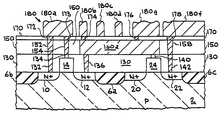
- FIG. 3is a fragmentary vertical cross-sectional view of the integrated circuit structure of the invention showing local interconnects formed over a first dielectric layer formed over the semiconductor substrate, with a thin dielectric layer formed over the local interconnects to separate them from a layer of metal interconnects formed over the thin dielectric layer.
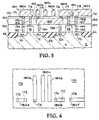
- FIG. 4is a fragmentary top view of the structure of FIG. 3 .
- FIG. 5is a fragmentary vertical cross-sectional view of the integrated circuit structure of the invention similar to FIG. 3 showing local interconnects formed over a first dielectric layer formed over the semiconductor substrate, with one of the local interconnects bridging over an underlying conductive region.
- the inventioncomprises an integrated circuit structure provided with a local interconnect layer and a first metal interconnect layer which are both capable of bridging over underlying conductive regions.
- the structurecomprises a first dielectric layer formed over the underlying integrated circuit structure to a height or thickness preferably exceeding the height of the highest conductive regions of the underlying integrated circuit devices, which usually will be the gate electrode; a second dielectric layer formed above the first dielectric layer; one or more local interconnects formed in the second dielectric layer; a thin third dielectric layer formed over the second dielectric layer and the local interconnects therein, wherein the third dielectric layer has a thickness not exceeding about 2000 ⁇ , and preferably ranging from about 1000 ⁇ to about 1500 ⁇ ; and a first layer of metal interconnects formed over the thin third dielectric layer.
- Conventionally formed filled contact openingsextend from the substrate through the first dielectric layer to either filled vias or a local interconnect in the second dielectric layer.
- the metal interconnectsare electrically connected to either filled vias or one or more local interconnects in the second dielectric layer by filled shallow vias in the third dielectric layer.
- the shallow vias in the thin third dielectric layerare preferably filled with the same materials and desirably at the same time as that used to form the first layer of metal interconnects.
- the term “local interconnect”is intended to mean the first patterned layer of interconnects formed above the substrate and formed from a conductive material having a higher resistance than the higher levels of patterned metal interconnect layers.
- thin dielectricherein is meant a dielectric material not exceeding about 2000 ⁇ in thickness and preferably having a thickness ranging from about 1000 ⁇ to about 1500 ⁇ , although even thinner dielectric layers may be used in some instances. This is in contrast to the conventional dielectric layer between local interconnects and metal interconnects (or between layers of metal interconnects) having a thickness usually ranging from about 7000 ⁇ to about 10,000 ⁇ .
- the use of a thin dielectric layer between the local interconnect layer and the first metal interconnect layermeans that the height or thickness of a via through this thin dielectric layer does not unduly increase the resistance because of the short additional path of the via through the thin dielectric layer.
- the aspect ratio of the viawas lowered, thus making it possible to eliminate the use of the high resistance tungsten metal filler (which is normally used to fill vias with high aspect ratios because of the superior via-filling ability of tungsten).
- the shallow viascan be filled at the same time (and with the same low resistance material) as the blanket deposition of the metal layer over the thin dielectric layer, e.g., the aluminum or copper layer which will be patterned to form the metal interconnects. Since the shallow (low aspect ratio) via can be filled with the same low resistance metal used to form the metal interconnects, and since the via height is very short (1000 ⁇ to 2000 ⁇ compared to 7000 ⁇ to 10,000 ⁇ ), the resistance added to the circuit by the presence of the thin dielectric of the invention is negligible.
- the thin dielectric of the inventionis the negligible effect of the thin dielectric of the invention on the overall capacitance of the integrated circuit structure.
- the aspect ratioheight/width
- the width of the interconnects or lineswas sufficiently large so that the vertical capacitance, i.e., the capacitance through the thickness of the dielectric layer from one level of interconnect to the next level, contributed most of the capacitance of the circuit, thus resulting in the need and use of thick dielectric layers.
- the aspect ratiosincreased and the line widths decreased the vertical component of the capacitance decreased.
- the horizontal spacing between vias and between linesshrank sufficiently so that the horizontal capacitance between adjacent conductive surfaces, such as between adjacent lines, has increased, thereby becoming a major contributor to the overall capacitance of the circuitry.
- the thickness of the dielectric layershas not changed, despite such changes in aspect ratios and linewidths, because at higher metal interconnect layer levels, the length of the lines, and the number of crossings of lines, is such that vertical capacitance still is a major contributor to capacitance.
- the first dielectric layer separating the local interconnect layer and the first metal interconnect layercould be made considerably thinner without unduly increasing the overall capacitance of the circuitry, because of the greater contribution of the horizontal capacitance to the overall capacitance of the circuitry (at least at such local interconnect/first metal interconnect levels).
- the inventionis principally directed to the local interconnect and first metal interconnect levels, and the separation of these two levels by a special thin dielectric layer, there may be some instances where the provision of such a thin dielectric layer between the first and second metal interconnect layers may also be appropriate, depending upon the density of the interconnects and the number of crossovers between such levels which could, if too high, add an unacceptable amount of capacitance to the integrated circuit structure if such a thin dielectric layer was used. Thus, under appropriate circumstances where the additional vertical capacitance will be insignificant, it is within the scope of the invention to also utilize the thin dielectric layer of the invention between the first and second levels of metal interconnects.
- the utility of the inventionis particularly directed toward the lowest levels of interconnects such as the local interconnect and first metal interconnect levels (and possibly between the first and second metal interconnect levels), where the length of the lines is short, to thereby minimize added vertical capacitance.
- shortwith respect to line and interconnect length, is meant not more than about 50 microns in length, preferably not more than about 20 microns, more preferably about 10 microns, and most preferably not more than about 5 microns in length.
- a semiconductor substrate 2may be provided, by way of example, with several MOS transistors constructed thereon which are electrically isolated from one another by field oxide 6 a , and from other devices in substrate 2 by field oxide 6 b and 6 c .
- the illustrated MOS devicesrespectively comprise source/drain regions 10 and 12 with a gate electrode 14 therebetween; and source/drain. regions 20 and 22 with a gate electrode 24 therebetween.
- a first dielectric layer 130formed of a dielectric material such as silicon oxide (SiO 2 ), is deposited over this structure and then planarized back, by an etch step or a chemical mechanical polishing process, to a level which is preferable slightly higher that gate electrodes 14 and 24 (which range in height from about 3500 ⁇ to about 5000 ⁇ ). By slightly higher is meant from about 500 ⁇ to about 1000 ⁇ higher than the top of gate electrodes 14 and 24 .
- Contact openings 132 , 134 , 136 , 138 , 140 , and 142are then cut through dielectric layer and filled with a conductive metal such as tungsten capable of filling a contact opening having a diameter of, for example, approximately 0.25 micrometers ( ⁇ m).
- a conductive metalsuch as tungsten capable of filling a contact opening having a diameter of, for example, approximately 0.25 micrometers ( ⁇ m).
- the surface of the structuremay be again planarized at this time, for example, by chemical mechanical polishing (CMP), to remove any of the contact opening filler material from the surface of dielectric layer 130 .
- CMPchemical mechanical polishing
- a second dielectric layer 150is then formed over dielectric layer 130 to a thickness which, when added to the thickness of dielectric layer 130 , will equal a total thickness of both dielectric layers of from about 7000 ⁇ to about 10,000 ⁇ .
- Openingsare then cut through dielectric layer 150 for the formation of vias to the previously described underlying filled contact openings, as well as for formation of local interconnects.
- the filled viassuch as illustrated filled vias 152 , 154 , 157 , and 158 , and the local interconnects, such as illustrated local interconnect 160 , are then formed by filling the openings with a conductive material (such as tungsten) capable of filling vias having a diameter of, for example, approximately 0.25 ⁇ m.
- the structuremay then be subject to a further planarization, such as a dry etch step or a chemical mechanical polishing step to remove the filler material form the surface of dielectric material 150 .
- a third dielectric layer 170comprising a thin dielectric layer, is formed over dielectric layer 150 after the formation of the filled vias, e.g., filled vias 152 - 158 , and the local interconnects, e.g., local interconnect 160 .
- Thin third dielectric layer 170is formed over dielectric layer 150 to a thickness not exceeding about 2000 ⁇ , and preferably ranging from about 1000 ⁇ to about 1500 ⁇ , although in some instances, dielectric layer 170 may be as thin as 500 ⁇ .
- This dielectric layermay again comprise silicon oxide (SiO 2 ).
- thin dielectric layer 170may comprise a material having an even lower dielectric constant than silicon oxide (i.e., lower than 3.8) to further reduce any capacitance added to the integrated circuit structure by the presence of third dielectric layer 170 .
- dielectric materials having dielectric constants less than 3.5include fluorinated perylene, fluorinated SiO 2 , and hydrogen silsesquioxane.
- Lower dielectric constant materials for use in the formation of thin dielectric layer 170can also be formed from modified silicon oxide, as described and claimed in U.S. Pat. Nos. 5,393,712, 5,470,801, and 5,598,026, all assigned to the assignee of this invention.
- viasare cut through layer 170 to the previously described underlying filled vias and local interconnects as desired.
- vias 172 , 173 , 174 and 176 , 177 , 178are cut through dielectric layer 170 to respectively connect with underlying filled vias 152 and 154 , local interconnect 160 , and filled vias 157 and 158 .
- the diameters of vias 172 , 173 , 174 and 176 , 177 , 178are preferably the same as that of previously formed vias 152 et al., i.e., about 0.25 ⁇ m.
- forming vias through layer 170 with the same diameter as the vias through layer 150results in the formation of vias in layer 170 of much smaller aspect ratios (height/width) than the vias previously formed in layer 150 .
- the need for a separate step to fill the shallow vias formed in thin dielectric layer 170 with special filler material, e.g., tungsten,can be eliminated. That is, the shallow low aspect ratio vias cut through dielectric layer 170 may be filled during the subsequent blanket deposit of a patternable metal, such as aluminum, over dielectric layer 170 for the formation of the first metal interconnect layer.
- a patternable metalsuch as aluminum
- an added bonus of the practice of the inventionis that the photoresist etch mask used to form the shallow vias through thin insulation layer 170 need not be a thick photoresist layer, since the via-etching step is very short (due to the thinness of dielectric layer 170 ) and therefore less of the photoresist mask will be eroded.
- the use of a thinner photoresist maskin turn, will increase the resolution and accuracy of pattern size and generally improve the masking process.
- the filling of vias 172 , 173 , 174 and 176 , 177 , 178 with the same metal used to form the first layer of metal interconnectsis advantageous from the standpoint of the lower resistance of metal interconnect material, such as aluminum (or copper), compared to conventional via filler materials, such as tungsten (which are selected for their via-filling capabilities, not their low resistance).
- metal interconnect materialsuch as aluminum (or copper)
- conventional via filler materialssuch as tungsten (which are selected for their via-filling capabilities, not their low resistance).
- a blanket layer of a patternable metalsuch as aluminum is deposited over dielectric layer 170 and into (and filling) vias 172 , 173 , 174 and 176 , 177 , 178 , in preparation for the formation of metal interconnects 180 a - 180 f .
- the metal layeris patterned, as shown in FIGS. 3 and 4, using a suitable photoresist mask and an anisotropic etch system, such as a chlorine plasma etch for aluminum.
- anisotropic etchwill normally be designed to stop at dielectric layer 170 , overetching into layer 170 , or even entirely through layer 170 to underlying dielectric layer 150 , is harmless, since a further dielectric layer will be deposited over and in between metal interconnects 180 a - 180 f (arid over any exposed surfaces of dielectric layers 150 and 170 in between the metal interconnects) after the formation of the metal interconnects.
- local interconnect 160 of FIG. 3has been replaced by local interconnect 160 a which is electrically connected to source/drain 12 through filled contact opening 136 and to gate electrode 24 through filled contact opening 140 .
- local interconnect 160 ais shown bridging over source/drain 20 .
- Local interconnect 160 ais shown connected to metal interconnect 180 b by filled via 174 and to metal interconnect 180 g by filled via 176 .
- the filled vias formed in layer 150 and the local interconnectsare in registry and in contact with the respective underlying filled contact openings to thereby complete the respective electrical paths, for example, from source/drain region 10 to metal interconnect 180 a through filled contact opening 132 , filled via 152 , and filled via 172 .
- a thin layer of coppermay be first deposited over dielectric layer 170 to fill vias 172 , 173 , 174 and 176 , 177 , 178 with copper, followed by a chemical mechanical polishing step to remove any copper from the surface of layer 170 .
- a fourth dielectric layermay then be deposited over layer 170 and etched to form trenches through the entire thickness of the fourth dielectric layer, the trenches corresponding to the desired pattern of metal interconnects, thereby exposing the copper-filled vias.
- a layer of copperis then deposited over the fourth dielectric layer and in the trenches, thereby making contact with the copper-filled vias.
- the structureis then subject to a further chemical mechanical polishing to remove all copper on the surface of the fourth dielectric layer, leaving the desired pattern of copper interconnects in the trenches.
- the resultis an integrated circuit structure having a local interconnect level capable of bridging conductive regions in the substrate, and a first metal interconnect level separated from the local interconnect level by a thin dielectric layer.
- the thin dielectric layerhaving a thickness not exceeding about 2000 ⁇ , and preferably having a thickness range of from about 1000 ⁇ to about 1500 ⁇ , does not add significant resistance or capacitance to the circuit.
- the added resistanceis minimal because of the reduced path length of the additional via through the thin dielectric layer and the reduced aspect ratio of the vias through the thin dielectric layer which makes possible the filling of the vias in the thin dielectric layer with the same low resistance metal used to form the metal interconnect level.
- the added capacitanceis minimal because of the low density of crossover lines between the local interconnect/first metal interconnect levels and the close horizontal spacing between adjacent vias and/or adjacent lines which provides the majority of the capacitance as horizontal components, and reduces the significance of vertical capacitance components.
Landscapes
- Engineering & Computer Science (AREA)
- Physics & Mathematics (AREA)
- Condensed Matter Physics & Semiconductors (AREA)
- General Physics & Mathematics (AREA)
- Manufacturing & Machinery (AREA)
- Computer Hardware Design (AREA)
- Microelectronics & Electronic Packaging (AREA)
- Power Engineering (AREA)
- Internal Circuitry In Semiconductor Integrated Circuit Devices (AREA)
Abstract
Description
Claims (6)
Priority Applications (1)
| Application Number | Priority Date | Filing Date | Title |
|---|---|---|---|
| US09/790,821US6486056B2 (en) | 1998-05-18 | 2001-02-22 | Process for making integrated circuit structure with thin dielectric between at least local interconnect level and first metal interconnect level |
Applications Claiming Priority (2)
| Application Number | Priority Date | Filing Date | Title |
|---|---|---|---|
| US09/081,403US6239491B1 (en) | 1998-05-18 | 1998-05-18 | Integrated circuit structure with thin dielectric between at least local interconnect level and first metal interconnect level, and process for making same |
| US09/790,821US6486056B2 (en) | 1998-05-18 | 2001-02-22 | Process for making integrated circuit structure with thin dielectric between at least local interconnect level and first metal interconnect level |
Related Parent Applications (1)
| Application Number | Title | Priority Date | Filing Date |
|---|---|---|---|
| US09/081,403DivisionUS6239491B1 (en) | 1998-05-18 | 1998-05-18 | Integrated circuit structure with thin dielectric between at least local interconnect level and first metal interconnect level, and process for making same |
Publications (2)
| Publication Number | Publication Date |
|---|---|
| US20010005057A1 US20010005057A1 (en) | 2001-06-28 |
| US6486056B2true US6486056B2 (en) | 2002-11-26 |
Family
ID=22163927
Family Applications (2)
| Application Number | Title | Priority Date | Filing Date |
|---|---|---|---|
| US09/081,403Expired - LifetimeUS6239491B1 (en) | 1998-05-18 | 1998-05-18 | Integrated circuit structure with thin dielectric between at least local interconnect level and first metal interconnect level, and process for making same |
| US09/790,821Expired - LifetimeUS6486056B2 (en) | 1998-05-18 | 2001-02-22 | Process for making integrated circuit structure with thin dielectric between at least local interconnect level and first metal interconnect level |
Family Applications Before (1)
| Application Number | Title | Priority Date | Filing Date |
|---|---|---|---|
| US09/081,403Expired - LifetimeUS6239491B1 (en) | 1998-05-18 | 1998-05-18 | Integrated circuit structure with thin dielectric between at least local interconnect level and first metal interconnect level, and process for making same |
Country Status (1)
| Country | Link |
|---|---|
| US (2) | US6239491B1 (en) |
Cited By (14)
| Publication number | Priority date | Publication date | Assignee | Title |
|---|---|---|---|---|
| US6765272B2 (en)* | 2001-04-27 | 2004-07-20 | Nec Electronics Corporation | Semiconductor device |
| US20050062044A1 (en)* | 2003-09-19 | 2005-03-24 | Semiconductor Energy Laboratory Co., Ltd. | Semiconductor device, method of manufacturing the same, and electronic device having the same |
| US20060019488A1 (en)* | 2004-07-23 | 2006-01-26 | Jhon-Jhy Liaw | Method of forming a static random access memory with a buried local interconnect |
| US20080074692A1 (en)* | 2006-09-25 | 2008-03-27 | Brother Kogyo Kabushiki Kaisha | Image Forming Apparatus |
| US20080079994A1 (en)* | 2006-09-28 | 2008-04-03 | Brother Kogyo Kabushiki Kaisha | Image forming apparatus and computer program product |
| US20080080007A1 (en)* | 2006-09-28 | 2008-04-03 | Brother Kogyo Kabushiki Kaisha | Image Forming Apparatus and Computer Program Product |
| US20080082914A1 (en)* | 2006-09-29 | 2008-04-03 | Brother Kogyo Kabushiki Kaisha | Document data edit device, documentation system, and computer program product |
| US20080189574A1 (en)* | 2006-09-28 | 2008-08-07 | Brother Kogyo Kabushiki Kaisha | Data processing apparatus and recording medium |
| US20080232882A1 (en)* | 2006-09-19 | 2008-09-25 | Brother Kogyo Kabushiki Kaisha | Printed Medium Management Apparatus |
| US20110284862A1 (en)* | 2010-05-24 | 2011-11-24 | International Rectifier Corporation | III-nitride switching device with an emulated diode |
| US20130069236A1 (en)* | 2011-09-21 | 2013-03-21 | Taiwan Semiconductor Manufacturing Co., Ltd. | Efficient semiconductor device cell layout utilizing underlying local connective features |
| US8947902B2 (en) | 2012-03-06 | 2015-02-03 | Taiwan Semiconductor Manufacturing Co., Ltd. | Semiconductor memory and method of making the same |
| US9349436B2 (en) | 2012-03-06 | 2016-05-24 | Taiwan Semiconductor Manufacturing Co., Ltd. | Semiconductor memory and method of making the same |
| US10031989B2 (en) | 2014-11-18 | 2018-07-24 | Globalfoundries Inc. | Integrated circuit performance modeling using a connectivity-based condensed resistance model for a conductive structure in an integrated circuit |
Families Citing this family (20)
| Publication number | Priority date | Publication date | Assignee | Title |
|---|---|---|---|---|
| US6448631B2 (en)* | 1998-09-23 | 2002-09-10 | Artisan Components, Inc. | Cell architecture with local interconnect and method for making same |
| EP0989609B1 (en)* | 1998-09-25 | 2005-02-09 | STMicroelectronics S.r.l. | Multilevel Interconnect Structure |
| US7271489B2 (en)* | 2003-10-15 | 2007-09-18 | Megica Corporation | Post passivation interconnection schemes on top of the IC chips |
| DE10142690A1 (en)* | 2001-08-31 | 2003-03-27 | Infineon Technologies Ag | Contacting the emitter contact of a semiconductor device |
| US6855624B1 (en) | 2002-09-17 | 2005-02-15 | Lsi Logic Corporation | Low-loss on-chip transmission line for integrated circuit structures and method of manufacture |
| US6969909B2 (en)* | 2002-12-20 | 2005-11-29 | Vlt, Inc. | Flip chip FET device |
| US7038917B2 (en)* | 2002-12-27 | 2006-05-02 | Vlt, Inc. | Low loss, high density array interconnection |
| DE10305365B4 (en)* | 2003-02-10 | 2005-02-10 | Infineon Technologies Ag | Method and arrangement for contacting terminals of a bipolar transistor |
| ITTO20060329A1 (en) | 2006-05-05 | 2007-11-06 | St Microelectronics Srl | SEMICONDUCTOR DEVICE WITH VERTICAL CURRENT FLOW AND LOW SUBSTRATE RESISTANCE AND PROCESS OF MANUFACTURE OF THIS DEVICE |
| JP4415984B2 (en)* | 2006-12-06 | 2010-02-17 | ソニー株式会社 | Manufacturing method of semiconductor device |
| US7608538B2 (en) | 2007-01-05 | 2009-10-27 | International Business Machines Corporation | Formation of vertical devices by electroplating |
| US8952547B2 (en) | 2007-07-09 | 2015-02-10 | Taiwan Semiconductor Manufacturing Company, Ltd. | Semiconductor device with contact structure with first/second contacts formed in first/second dielectric layers and method of forming same |
| US8035165B2 (en)* | 2008-08-26 | 2011-10-11 | Taiwan Semiconductor Manufacturing Company, Ltd. | Integrating a first contact structure in a gate last process |
| US7981789B2 (en) | 2008-11-14 | 2011-07-19 | Infineon Technologies Ag | Feature patterning methods and structures thereof |
| US20110248283A1 (en)* | 2010-04-07 | 2011-10-13 | Jianjun Cao | Via structure of a semiconductor device and method for fabricating the same |
| KR102310122B1 (en)* | 2014-06-10 | 2021-10-08 | 삼성전자주식회사 | Logic cell, integrated circuit including logic cell, and methods of manufacturing the same |
| US9583485B2 (en)* | 2015-05-15 | 2017-02-28 | Taiwan Semiconductor Manufacturing Company, Ltd. | Fin field effect transistor (FinFET) device structure with uneven gate structure and method for forming the same |
| US10128187B2 (en)* | 2016-07-11 | 2018-11-13 | Globalfoundries Inc. | Integrated circuit structure having gate contact and method of forming same |
| US9881926B1 (en)* | 2016-10-24 | 2018-01-30 | International Business Machines Corporation | Static random access memory (SRAM) density scaling by using middle of line (MOL) flow |
| US11658215B2 (en)* | 2021-02-19 | 2023-05-23 | Taiwan Semiconductor Manufacturing Company, Ltd. | Method of forming contact structures |
Citations (26)
| Publication number | Priority date | Publication date | Assignee | Title |
|---|---|---|---|---|
| JPH01133354A (en)* | 1987-11-19 | 1989-05-25 | Sanyo Electric Co Ltd | Semiconductor integrated circuit and manufacture thereof |
| US5393712A (en) | 1993-06-28 | 1995-02-28 | Lsi Logic Corporation | Process for forming low dielectric constant insulation layer on integrated circuit structure |
| US5470801A (en) | 1993-06-28 | 1995-11-28 | Lsi Logic Corporation | Low dielectric constant insulation layer for integrated circuit structure and method of making same |
| US5495117A (en) | 1991-05-29 | 1996-02-27 | Ramtron International Corporation | Stacked ferroelectric memory cell |
| US5554867A (en) | 1993-12-27 | 1996-09-10 | Mitsubishi Denki Kabushiki Kaisha | Nonvolatile semiconductor memory device having a memory cell transistor and a select transistor |
| US5591673A (en) | 1995-07-05 | 1997-01-07 | Taiwan Semiconductor Manufacturing Company Ltd. | Tungsten stud process for stacked via applications |
| US5639692A (en) | 1996-04-08 | 1997-06-17 | Chartered Semiconductor Manufacturing Pte, Ltd. | Non-etch back SOG process using a metal via stud |
| US5759906A (en) | 1997-04-11 | 1998-06-02 | Industrial Technology Research Institute | Planarization method for intermetal dielectrics between multilevel interconnections on integrated circuits |
| US5767012A (en) | 1996-06-05 | 1998-06-16 | Advanced Micro Devices, Inc. | Method of forming a recessed interconnect structure |
| US5798568A (en) | 1996-08-26 | 1998-08-25 | Motorola, Inc. | Semiconductor component with multi-level interconnect system and method of manufacture |
| US5801419A (en) | 1993-10-15 | 1998-09-01 | Ixys Corporation | High frequency MOS device |
| US5801093A (en) | 1996-06-13 | 1998-09-01 | Taiwan Semiconductor Manufacturing Company, Ltd. | Process for creating vias using pillar technology |
| US5837557A (en) | 1997-03-14 | 1998-11-17 | Advanced Micro Devices, Inc. | Semiconductor fabrication method of forming a master layer to combine individually printed blocks of a circuit pattern |
| US5840624A (en) | 1996-03-15 | 1998-11-24 | Taiwan Semiconductor Manufacturing Company, Ltd | Reduction of via over etching for borderless contacts |
| US5850102A (en)* | 1996-04-03 | 1998-12-15 | Kabushiki Kaisha Toshiba | Semiconductor device having a second insulating layer which includes carbon or fluorine at a density lower than a first insulating layer |
| US5858869A (en) | 1997-06-03 | 1999-01-12 | Industrial Technology Research Institute | Method for fabricating intermetal dielectric insulation using anisotropic plasma oxides and low dielectric constant polymers |
| US5866923A (en) | 1995-11-08 | 1999-02-02 | Fujitsu Limited | Semiconductor integrated circuit device having fundamental cells and method of manufacturing the semiconductor integrated circuit device using the fundamental cells |
| US5869149A (en) | 1997-06-30 | 1999-02-09 | Lam Research Corporation | Method for preparing nitrogen surface treated fluorine doped silicon dioxide films |
| US5882983A (en) | 1997-12-19 | 1999-03-16 | Advanced Micro Devices, Inc. | Trench isolation structure partially bound between a pair of low K dielectric structures |
| US5886388A (en) | 1997-07-28 | 1999-03-23 | Mitsubishi Denki Kabushiki Kaisha | Static semiconductor memory device and manufacturing method thereof |
| US5892249A (en) | 1996-02-23 | 1999-04-06 | National Semiconductor Corporation | Integrated circuit having reprogramming cell |
| US5900668A (en) | 1995-11-30 | 1999-05-04 | Advanced Micro Devices, Inc. | Low capacitance interconnection |
| US5943598A (en) | 1995-10-19 | 1999-08-24 | Stmicroelectronics, Inc. | Integrated circuit with planarized dielectric layer between successive polysilicon layers |
| US5950102A (en)* | 1997-02-03 | 1999-09-07 | Industrial Technology Research Institute | Method for fabricating air-insulated multilevel metal interconnections for integrated circuits |
| US5970375A (en) | 1997-05-03 | 1999-10-19 | Advanced Micro Devices, Inc. | Semiconductor fabrication employing a local interconnect |
| US6107189A (en) | 1997-03-05 | 2000-08-22 | Micron Technology, Inc. | Method of making a local interconnect using spacer-masked contact etch |
- 1998
- 1998-05-18USUS09/081,403patent/US6239491B1/ennot_activeExpired - Lifetime
- 2001
- 2001-02-22USUS09/790,821patent/US6486056B2/ennot_activeExpired - Lifetime
Patent Citations (28)
| Publication number | Priority date | Publication date | Assignee | Title |
|---|---|---|---|---|
| JPH01133354A (en)* | 1987-11-19 | 1989-05-25 | Sanyo Electric Co Ltd | Semiconductor integrated circuit and manufacture thereof |
| US5495117A (en) | 1991-05-29 | 1996-02-27 | Ramtron International Corporation | Stacked ferroelectric memory cell |
| US5393712A (en) | 1993-06-28 | 1995-02-28 | Lsi Logic Corporation | Process for forming low dielectric constant insulation layer on integrated circuit structure |
| US5470801A (en) | 1993-06-28 | 1995-11-28 | Lsi Logic Corporation | Low dielectric constant insulation layer for integrated circuit structure and method of making same |
| US5598026A (en) | 1993-06-28 | 1997-01-28 | Lsi Logic Corporation | Low dielectric constant insulation layer for integrated circuit structure and method of making same |
| US5801419A (en) | 1993-10-15 | 1998-09-01 | Ixys Corporation | High frequency MOS device |
| US5554867A (en) | 1993-12-27 | 1996-09-10 | Mitsubishi Denki Kabushiki Kaisha | Nonvolatile semiconductor memory device having a memory cell transistor and a select transistor |
| US5591673A (en) | 1995-07-05 | 1997-01-07 | Taiwan Semiconductor Manufacturing Company Ltd. | Tungsten stud process for stacked via applications |
| US5943598A (en) | 1995-10-19 | 1999-08-24 | Stmicroelectronics, Inc. | Integrated circuit with planarized dielectric layer between successive polysilicon layers |
| US5866923A (en) | 1995-11-08 | 1999-02-02 | Fujitsu Limited | Semiconductor integrated circuit device having fundamental cells and method of manufacturing the semiconductor integrated circuit device using the fundamental cells |
| US5900668A (en) | 1995-11-30 | 1999-05-04 | Advanced Micro Devices, Inc. | Low capacitance interconnection |
| US5892249A (en) | 1996-02-23 | 1999-04-06 | National Semiconductor Corporation | Integrated circuit having reprogramming cell |
| US5840624A (en) | 1996-03-15 | 1998-11-24 | Taiwan Semiconductor Manufacturing Company, Ltd | Reduction of via over etching for borderless contacts |
| US5850102A (en)* | 1996-04-03 | 1998-12-15 | Kabushiki Kaisha Toshiba | Semiconductor device having a second insulating layer which includes carbon or fluorine at a density lower than a first insulating layer |
| US5639692A (en) | 1996-04-08 | 1997-06-17 | Chartered Semiconductor Manufacturing Pte, Ltd. | Non-etch back SOG process using a metal via stud |
| US5767012A (en) | 1996-06-05 | 1998-06-16 | Advanced Micro Devices, Inc. | Method of forming a recessed interconnect structure |
| US5801093A (en) | 1996-06-13 | 1998-09-01 | Taiwan Semiconductor Manufacturing Company, Ltd. | Process for creating vias using pillar technology |
| US5929525A (en)* | 1996-06-13 | 1999-07-27 | Taiwan Semiconductor Manufacturing Company, Ltd. | Process for creating vias using pillar technology |
| US5798568A (en) | 1996-08-26 | 1998-08-25 | Motorola, Inc. | Semiconductor component with multi-level interconnect system and method of manufacture |
| US5950102A (en)* | 1997-02-03 | 1999-09-07 | Industrial Technology Research Institute | Method for fabricating air-insulated multilevel metal interconnections for integrated circuits |
| US6107189A (en) | 1997-03-05 | 2000-08-22 | Micron Technology, Inc. | Method of making a local interconnect using spacer-masked contact etch |
| US5837557A (en) | 1997-03-14 | 1998-11-17 | Advanced Micro Devices, Inc. | Semiconductor fabrication method of forming a master layer to combine individually printed blocks of a circuit pattern |
| US5759906A (en) | 1997-04-11 | 1998-06-02 | Industrial Technology Research Institute | Planarization method for intermetal dielectrics between multilevel interconnections on integrated circuits |
| US5970375A (en) | 1997-05-03 | 1999-10-19 | Advanced Micro Devices, Inc. | Semiconductor fabrication employing a local interconnect |
| US5858869A (en) | 1997-06-03 | 1999-01-12 | Industrial Technology Research Institute | Method for fabricating intermetal dielectric insulation using anisotropic plasma oxides and low dielectric constant polymers |
| US5869149A (en) | 1997-06-30 | 1999-02-09 | Lam Research Corporation | Method for preparing nitrogen surface treated fluorine doped silicon dioxide films |
| US5886388A (en) | 1997-07-28 | 1999-03-23 | Mitsubishi Denki Kabushiki Kaisha | Static semiconductor memory device and manufacturing method thereof |
| US5882983A (en) | 1997-12-19 | 1999-03-16 | Advanced Micro Devices, Inc. | Trench isolation structure partially bound between a pair of low K dielectric structures |
Cited By (24)
| Publication number | Priority date | Publication date | Assignee | Title |
|---|---|---|---|---|
| US6765272B2 (en)* | 2001-04-27 | 2004-07-20 | Nec Electronics Corporation | Semiconductor device |
| US20050062044A1 (en)* | 2003-09-19 | 2005-03-24 | Semiconductor Energy Laboratory Co., Ltd. | Semiconductor device, method of manufacturing the same, and electronic device having the same |
| US7145210B2 (en)* | 2003-09-19 | 2006-12-05 | Semiconductor Energy Laboratory Co., Ltd. | Semiconductor device |
| US20070045730A1 (en)* | 2003-09-19 | 2007-03-01 | Semiconductor Energy Laboratory Co., Ltd. | Semiconductor device, method of manufacturing the same, and electronic device having the same |
| US8288831B2 (en) | 2003-09-19 | 2012-10-16 | Semiconductor Energy Laboratory Co., Ltd. | Semiconductor device, method of manufacturing the same, and electronic device having the same |
| US20110121408A1 (en)* | 2003-09-19 | 2011-05-26 | Semiconductor Energy Laboratory Co., Ltd. | Semiconductor device, method of manufacturing the same, and electronic device having the same |
| US7868398B2 (en) | 2003-09-19 | 2011-01-11 | Semiconductor Energy Laboratory Co., Ltd. | Semiconductor device |
| US20060019488A1 (en)* | 2004-07-23 | 2006-01-26 | Jhon-Jhy Liaw | Method of forming a static random access memory with a buried local interconnect |
| US7176125B2 (en)* | 2004-07-23 | 2007-02-13 | Taiwan Semiconductor Manufacturing Company, Ltd. | Method of forming a static random access memory with a buried local interconnect |
| US20080232882A1 (en)* | 2006-09-19 | 2008-09-25 | Brother Kogyo Kabushiki Kaisha | Printed Medium Management Apparatus |
| US20080074692A1 (en)* | 2006-09-25 | 2008-03-27 | Brother Kogyo Kabushiki Kaisha | Image Forming Apparatus |
| US20080079994A1 (en)* | 2006-09-28 | 2008-04-03 | Brother Kogyo Kabushiki Kaisha | Image forming apparatus and computer program product |
| US20080080007A1 (en)* | 2006-09-28 | 2008-04-03 | Brother Kogyo Kabushiki Kaisha | Image Forming Apparatus and Computer Program Product |
| US20080189574A1 (en)* | 2006-09-28 | 2008-08-07 | Brother Kogyo Kabushiki Kaisha | Data processing apparatus and recording medium |
| US8125670B2 (en) | 2006-09-28 | 2012-02-28 | Brother Kogyo Kabushiki Kaisha | Data processing apparatus and recording medium |
| US8179557B2 (en)* | 2006-09-28 | 2012-05-15 | Brother Kogyo Kabushiki Kaisha | Image forming apparatus for reading information from and writing information to a non-contact medium |
| US20080082914A1 (en)* | 2006-09-29 | 2008-04-03 | Brother Kogyo Kabushiki Kaisha | Document data edit device, documentation system, and computer program product |
| US20110284862A1 (en)* | 2010-05-24 | 2011-11-24 | International Rectifier Corporation | III-nitride switching device with an emulated diode |
| US9263439B2 (en)* | 2010-05-24 | 2016-02-16 | Infineon Technologies Americas Corp. | III-nitride switching device with an emulated diode |
| US20130069236A1 (en)* | 2011-09-21 | 2013-03-21 | Taiwan Semiconductor Manufacturing Co., Ltd. | Efficient semiconductor device cell layout utilizing underlying local connective features |
| US8816403B2 (en)* | 2011-09-21 | 2014-08-26 | Taiwan Semiconductor Manufacturing Co., Ltd. | Efficient semiconductor device cell layout utilizing underlying local connective features |
| US8947902B2 (en) | 2012-03-06 | 2015-02-03 | Taiwan Semiconductor Manufacturing Co., Ltd. | Semiconductor memory and method of making the same |
| US9349436B2 (en) | 2012-03-06 | 2016-05-24 | Taiwan Semiconductor Manufacturing Co., Ltd. | Semiconductor memory and method of making the same |
| US10031989B2 (en) | 2014-11-18 | 2018-07-24 | Globalfoundries Inc. | Integrated circuit performance modeling using a connectivity-based condensed resistance model for a conductive structure in an integrated circuit |
Also Published As
| Publication number | Publication date |
|---|---|
| US6239491B1 (en) | 2001-05-29 |
| US20010005057A1 (en) | 2001-06-28 |
Similar Documents
| Publication | Publication Date | Title |
|---|---|---|
| US6486056B2 (en) | Process for making integrated circuit structure with thin dielectric between at least local interconnect level and first metal interconnect level | |
| US11004832B2 (en) | System, structure, and method of manufacturing a semiconductor substrate stack | |
| US8390038B2 (en) | MIM capacitor and method of making same | |
| US6140238A (en) | Self-aligned copper interconnect structure and method of manufacturing same | |
| US6743644B2 (en) | Method of making a metallization line layout | |
| US4617193A (en) | Planar interconnect for integrated circuits | |
| US6468894B1 (en) | Metal interconnection structure with dummy vias | |
| US5663599A (en) | Metal layout pattern for improved passivation layer coverage | |
| JP3778487B2 (en) | Method for forming metal capacitor | |
| CN100541779C (en) | Semiconductor device and manufacturing method thereof | |
| US6472317B1 (en) | Dual damascene arrangement for metal interconnection with low k dielectric constant materials in dielectric layers | |
| EP1326276A2 (en) | Interconnection structure in semiconductor device | |
| US6348734B1 (en) | Self-aligned copper interconnect architecture with enhanced copper diffusion barrier | |
| KR20010076367A (en) | A capacitor for integration with copper damascene processes and a method of manufacture therefore | |
| JP2002118173A (en) | High capacitance damask capacitors | |
| EP0495974A1 (en) | Trench conductors and crossover architecture | |
| US7050290B2 (en) | Integrated capacitor | |
| JPH0214552A (en) | Method of forming at least one additional level metal interconnection so as to be brought into contact with metal of lower level in semiconductor device | |
| US20030109132A1 (en) | Method for forming dual damascene structure in semiconductor device | |
| US6017814A (en) | Structure and fabrication method for stackable, air-gap-containing low epsilon dielectric layers | |
| US5924006A (en) | Trench surrounded metal pattern | |
| JPH11186391A (en) | Semiconductor device and manufacturing method thereof | |
| JP2001053144A (en) | Semiconductor device and manufacturing method of the same | |
| US5915201A (en) | Trench surrounded metal pattern | |
| US6218291B1 (en) | Method for forming contact plugs and simultaneously planarizing a substrate surface in integrated circuits |
Legal Events
| Date | Code | Title | Description |
|---|---|---|---|
| STCF | Information on status: patent grant | Free format text:PATENTED CASE | |
| FPAY | Fee payment | Year of fee payment:4 | |
| FEPP | Fee payment procedure | Free format text:PAYOR NUMBER ASSIGNED (ORIGINAL EVENT CODE: ASPN); ENTITY STATUS OF PATENT OWNER: LARGE ENTITY | |
| FPAY | Fee payment | Year of fee payment:8 | |
| FPAY | Fee payment | Year of fee payment:12 | |
| AS | Assignment | Owner name:DEUTSCHE BANK AG NEW YORK BRANCH, AS COLLATERAL AG Free format text:PATENT SECURITY AGREEMENT;ASSIGNORS:LSI CORPORATION;AGERE SYSTEMS LLC;REEL/FRAME:032856/0031 Effective date:20140506 | |
| AS | Assignment | Owner name:AVAGO TECHNOLOGIES GENERAL IP (SINGAPORE) PTE. LTD Free format text:ASSIGNMENT OF ASSIGNORS INTEREST;ASSIGNOR:LSI CORPORATION;REEL/FRAME:035390/0388 Effective date:20140814 | |
| AS | Assignment | Owner name:AGERE SYSTEMS LLC, PENNSYLVANIA Free format text:TERMINATION AND RELEASE OF SECURITY INTEREST IN PATENT RIGHTS (RELEASES RF 032856-0031);ASSIGNOR:DEUTSCHE BANK AG NEW YORK BRANCH, AS COLLATERAL AGENT;REEL/FRAME:037684/0039 Effective date:20160201 Owner name:LSI CORPORATION, CALIFORNIA Free format text:TERMINATION AND RELEASE OF SECURITY INTEREST IN PATENT RIGHTS (RELEASES RF 032856-0031);ASSIGNOR:DEUTSCHE BANK AG NEW YORK BRANCH, AS COLLATERAL AGENT;REEL/FRAME:037684/0039 Effective date:20160201 | |
| AS | Assignment | Owner name:BANK OF AMERICA, N.A., AS COLLATERAL AGENT, NORTH CAROLINA Free format text:PATENT SECURITY AGREEMENT;ASSIGNOR:AVAGO TECHNOLOGIES GENERAL IP (SINGAPORE) PTE. LTD.;REEL/FRAME:037808/0001 Effective date:20160201 Owner name:BANK OF AMERICA, N.A., AS COLLATERAL AGENT, NORTH Free format text:PATENT SECURITY AGREEMENT;ASSIGNOR:AVAGO TECHNOLOGIES GENERAL IP (SINGAPORE) PTE. LTD.;REEL/FRAME:037808/0001 Effective date:20160201 | |
| AS | Assignment | Owner name:AVAGO TECHNOLOGIES GENERAL IP (SINGAPORE) PTE. LTD., SINGAPORE Free format text:TERMINATION AND RELEASE OF SECURITY INTEREST IN PATENTS;ASSIGNOR:BANK OF AMERICA, N.A., AS COLLATERAL AGENT;REEL/FRAME:041710/0001 Effective date:20170119 Owner name:AVAGO TECHNOLOGIES GENERAL IP (SINGAPORE) PTE. LTD Free format text:TERMINATION AND RELEASE OF SECURITY INTEREST IN PATENTS;ASSIGNOR:BANK OF AMERICA, N.A., AS COLLATERAL AGENT;REEL/FRAME:041710/0001 Effective date:20170119 | |
| AS | Assignment | Owner name:BELL SEMICONDUCTOR, LLC, ILLINOIS Free format text:ASSIGNMENT OF ASSIGNORS INTEREST;ASSIGNORS:AVAGO TECHNOLOGIES GENERAL IP (SINGAPORE) PTE. LTD.;BROADCOM CORPORATION;REEL/FRAME:044886/0001 Effective date:20171208 Owner name:BELL SEMICONDUCTOR, LLC, ILLINOIS Free format text:ASSIGNMENT OF ASSIGNORS INTEREST;ASSIGNORS:AVAGO TECHNOLOGIES GENERAL IP (SINGAPORE) PTE. LTD.;BROADCOM CORPORATION;REEL/FRAME:044886/0608 Effective date:20171208 | |
| AS | Assignment | Owner name:CORTLAND CAPITAL MARKET SERVICES LLC, AS COLLATERA Free format text:SECURITY INTEREST;ASSIGNORS:HILCO PATENT ACQUISITION 56, LLC;BELL SEMICONDUCTOR, LLC;BELL NORTHERN RESEARCH, LLC;REEL/FRAME:045216/0020 Effective date:20180124 | |
| AS | Assignment | Owner name:BELL NORTHERN RESEARCH, LLC, ILLINOIS Free format text:SECURITY INTEREST;ASSIGNOR:CORTLAND CAPITAL MARKET SERVICES LLC;REEL/FRAME:060885/0001 Effective date:20220401 Owner name:BELL SEMICONDUCTOR, LLC, ILLINOIS Free format text:SECURITY INTEREST;ASSIGNOR:CORTLAND CAPITAL MARKET SERVICES LLC;REEL/FRAME:060885/0001 Effective date:20220401 Owner name:HILCO PATENT ACQUISITION 56, LLC, ILLINOIS Free format text:SECURITY INTEREST;ASSIGNOR:CORTLAND CAPITAL MARKET SERVICES LLC;REEL/FRAME:060885/0001 Effective date:20220401 Owner name:BELL NORTHERN RESEARCH, LLC, ILLINOIS Free format text:RELEASE BY SECURED PARTY;ASSIGNOR:CORTLAND CAPITAL MARKET SERVICES LLC;REEL/FRAME:059720/0719 Effective date:20220401 Owner name:BELL SEMICONDUCTOR, LLC, ILLINOIS Free format text:RELEASE BY SECURED PARTY;ASSIGNOR:CORTLAND CAPITAL MARKET SERVICES LLC;REEL/FRAME:059720/0719 Effective date:20220401 Owner name:HILCO PATENT ACQUISITION 56, LLC, ILLINOIS Free format text:RELEASE BY SECURED PARTY;ASSIGNOR:CORTLAND CAPITAL MARKET SERVICES LLC;REEL/FRAME:059720/0719 Effective date:20220401 |