US6483355B1 - Single chip CMOS transmitter/receiver and method of using same - Google Patents
Single chip CMOS transmitter/receiver and method of using sameDownload PDFInfo
- Publication number
- US6483355B1 US6483355B1US09/709,637US70963700AUS6483355B1US 6483355 B1US6483355 B1US 6483355B1US 70963700 AUS70963700 AUS 70963700AUS 6483355 B1US6483355 B1US 6483355B1
- Authority
- US
- United States
- Prior art keywords
- signals
- signal
- coupled
- communication system
- filter
- Prior art date
- Legal status (The legal status is an assumption and is not a legal conclusion. Google has not performed a legal analysis and makes no representation as to the accuracy of the status listed.)
- Expired - Lifetime
Links
- 238000000034methodMethods0.000titleclaimsabstractdescription16
- 238000004891communicationMethods0.000claimsabstractdescription50
- 230000003321amplificationEffects0.000claimsabstractdescription15
- 238000003199nucleic acid amplification methodMethods0.000claimsabstractdescription15
- 238000006243chemical reactionMethods0.000claimsdescription31
- 238000001914filtrationMethods0.000claimsdescription8
- 238000012545processingMethods0.000claimsdescription5
- 238000010586diagramMethods0.000description14
- 230000010354integrationEffects0.000description7
- 238000005516engineering processMethods0.000description6
- 101100350613Arabidopsis thaliana PLL1 geneProteins0.000description4
- 101100082028Arabidopsis thaliana PLL2 geneProteins0.000description4
- 230000005540biological transmissionEffects0.000description3
- 230000015556catabolic processEffects0.000description3
- 238000006731degradation reactionMethods0.000description3
- 230000000903blocking effectEffects0.000description2
- 230000000737periodic effectEffects0.000description2
- 229910001218Gallium arsenideInorganic materials0.000description1
- 239000000969carrierSubstances0.000description1
- 238000002347injectionMethods0.000description1
- 239000007924injectionSubstances0.000description1
- 238000012986modificationMethods0.000description1
- 230000004048modificationEffects0.000description1
- 230000010363phase shiftEffects0.000description1
- 229920000729poly(L-lysine) polymerPolymers0.000description1
- 230000005855radiationEffects0.000description1
- 238000005070samplingMethods0.000description1
- 239000000758substrateSubstances0.000description1
- 238000012546transferMethods0.000description1
Images


Classifications
- H—ELECTRICITY
- H04—ELECTRIC COMMUNICATION TECHNIQUE
- H04B—TRANSMISSION
- H04B1/00—Details of transmission systems, not covered by a single one of groups H04B3/00 - H04B13/00; Details of transmission systems not characterised by the medium used for transmission
- H04B1/38—Transceivers, i.e. devices in which transmitter and receiver form a structural unit and in which at least one part is used for functions of transmitting and receiving
- H04B1/40—Circuits
- H04B1/403—Circuits using the same oscillator for generating both the transmitter frequency and the receiver local oscillator frequency
- H—ELECTRICITY
- H03—ELECTRONIC CIRCUITRY
- H03H—IMPEDANCE NETWORKS, e.g. RESONANT CIRCUITS; RESONATORS
- H03H11/00—Networks using active elements
- H03H11/02—Multiple-port networks
- H03H11/16—Networks for phase shifting
- H03H11/22—Networks for phase shifting providing two or more phase shifted output signals, e.g. n-phase output
- H—ELECTRICITY
- H03—ELECTRONIC CIRCUITRY
- H03K—PULSE TECHNIQUE
- H03K9/00—Demodulating pulses which have been modulated with a continuously-variable signal
- H—ELECTRICITY
- H03—ELECTRONIC CIRCUITRY
- H03L—AUTOMATIC CONTROL, STARTING, SYNCHRONISATION OR STABILISATION OF GENERATORS OF ELECTRONIC OSCILLATIONS OR PULSES
- H03L7/00—Automatic control of frequency or phase; Synchronisation
- H03L7/06—Automatic control of frequency or phase; Synchronisation using a reference signal applied to a frequency- or phase-locked loop
- H03L7/08—Details of the phase-locked loop
- H03L7/099—Details of the phase-locked loop concerning mainly the controlled oscillator of the loop
- H03L7/0995—Details of the phase-locked loop concerning mainly the controlled oscillator of the loop the oscillator comprising a ring oscillator
- H—ELECTRICITY
- H03—ELECTRONIC CIRCUITRY
- H03L—AUTOMATIC CONTROL, STARTING, SYNCHRONISATION OR STABILISATION OF GENERATORS OF ELECTRONIC OSCILLATIONS OR PULSES
- H03L7/00—Automatic control of frequency or phase; Synchronisation
- H03L7/06—Automatic control of frequency or phase; Synchronisation using a reference signal applied to a frequency- or phase-locked loop
- H03L7/16—Indirect frequency synthesis, i.e. generating a desired one of a number of predetermined frequencies using a frequency- or phase-locked loop
- H03L7/18—Indirect frequency synthesis, i.e. generating a desired one of a number of predetermined frequencies using a frequency- or phase-locked loop using a frequency divider or counter in the loop
- H03L7/197—Indirect frequency synthesis, i.e. generating a desired one of a number of predetermined frequencies using a frequency- or phase-locked loop using a frequency divider or counter in the loop a time difference being used for locking the loop, the counter counting between numbers which are variable in time or the frequency divider dividing by a factor variable in time, e.g. for obtaining fractional frequency division
- H03L7/1974—Indirect frequency synthesis, i.e. generating a desired one of a number of predetermined frequencies using a frequency- or phase-locked loop using a frequency divider or counter in the loop a time difference being used for locking the loop, the counter counting between numbers which are variable in time or the frequency divider dividing by a factor variable in time, e.g. for obtaining fractional frequency division for fractional frequency division
- H—ELECTRICITY
- H04—ELECTRIC COMMUNICATION TECHNIQUE
- H04B—TRANSMISSION
- H04B1/00—Details of transmission systems, not covered by a single one of groups H04B3/00 - H04B13/00; Details of transmission systems not characterised by the medium used for transmission
- H04B1/06—Receivers
- H04B1/16—Circuits
- H04B1/18—Input circuits, e.g. for coupling to an antenna or a transmission line
- H—ELECTRICITY
- H04—ELECTRIC COMMUNICATION TECHNIQUE
- H04B—TRANSMISSION
- H04B1/00—Details of transmission systems, not covered by a single one of groups H04B3/00 - H04B13/00; Details of transmission systems not characterised by the medium used for transmission
- H04B1/06—Receivers
- H04B1/16—Circuits
- H04B1/26—Circuits for superheterodyne receivers
- H04B1/28—Circuits for superheterodyne receivers the receiver comprising at least one semiconductor device having three or more electrodes
- H—ELECTRICITY
- H04—ELECTRIC COMMUNICATION TECHNIQUE
- H04B—TRANSMISSION
- H04B1/00—Details of transmission systems, not covered by a single one of groups H04B3/00 - H04B13/00; Details of transmission systems not characterised by the medium used for transmission
- H04B1/38—Transceivers, i.e. devices in which transmitter and receiver form a structural unit and in which at least one part is used for functions of transmitting and receiving
- H04B1/40—Circuits
- H—ELECTRICITY
- H03—ELECTRONIC CIRCUITRY
- H03F—AMPLIFIERS
- H03F2200/00—Indexing scheme relating to amplifiers
- H03F2200/372—Noise reduction and elimination in amplifier
- H—ELECTRICITY
- H03—ELECTRONIC CIRCUITRY
- H03H—IMPEDANCE NETWORKS, e.g. RESONANT CIRCUITS; RESONATORS
- H03H11/00—Networks using active elements
- H03H11/02—Multiple-port networks
- H03H11/04—Frequency selective two-port networks
- H03H2011/0494—Complex filters
- H—ELECTRICITY
- H03—ELECTRONIC CIRCUITRY
- H03L—AUTOMATIC CONTROL, STARTING, SYNCHRONISATION OR STABILISATION OF GENERATORS OF ELECTRONIC OSCILLATIONS OR PULSES
- H03L7/00—Automatic control of frequency or phase; Synchronisation
- H03L7/06—Automatic control of frequency or phase; Synchronisation using a reference signal applied to a frequency- or phase-locked loop
- H03L7/08—Details of the phase-locked loop
- H03L7/085—Details of the phase-locked loop concerning mainly the frequency- or phase-detection arrangement including the filtering or amplification of its output signal
- H03L7/089—Details of the phase-locked loop concerning mainly the frequency- or phase-detection arrangement including the filtering or amplification of its output signal the phase or frequency detector generating up-down pulses
- H03L7/0891—Details of the phase-locked loop concerning mainly the frequency- or phase-detection arrangement including the filtering or amplification of its output signal the phase or frequency detector generating up-down pulses the up-down pulses controlling source and sink current generators, e.g. a charge pump
Definitions
- the present inventionrelates to a communication system, and in particular, to a CMOS radio frequency (RF) communication system.
- RFradio frequency
- a radio frequency (RF) communications systemhas a variety of applications including PCS communication and IMT systems.
- a CMOS chip integration of the systemhas been pursued to reduce the cost, size and power consumption.
- the RF communication systemis composed of RF front-end block and base-band digital signal processing DSP) block or baseband modem block.
- the base-band DSP blockcan be implemented with low cost and low power CMOS technology.
- the RF front-endcannot be implemented by CMOS technology because of limitations in speed, bandwidth and noise characteristics, which are below the speed, the frequency and noise specifications of popular RF communication systems.
- the PCS hand-phone systemsoperate at a frequency over 2.0 GHz, but current CMOS technology reliably operates only up to approximately 1.0 GHz in terms of speed and noise.
- the RF front-end blockis implemented using bipolar, bi-CMOS or GaAs technology that has better speed, bandwidth and noise characteristics than CMOS technology but is more expensive and consumes more power.
- CMOS RF communication systemsTwo different types of RF architecture called “direct conversion” and super-heterodyne (double conversion) are used for CMOS RF communication systems. Both architectures have advantages and disadvantages in terms of CMOS implementations.
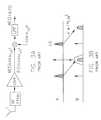
- FIG. 1is a diagram showing a related art direct conversion RF system 100 .
- a related art direct conversion CMOS RF communication system 100includes an antenna 105 , a RF filter 110 , a low noise amplifier (LNA) 120 , a phase-locked loop (PLL) 130 , a first mixer 140 , a second mixer 142 , first and second amplifiers 150 , 152 , a first low pass filter (LPF) 160 , a second LPF 162 , first and second variable gain amplifiers (VGA) 170 , 172 each including automatic gain control (AGC) loops, a first analog/digital (A/D) converter 180 , a second A/D converter 182 , a third mixer 190 and a power amplifier 192 .
- LNAlow noise amplifier
- PLLphase-locked loop
- LPFlow pass filter
- VGAvariable gain amplifiers
- the antenna 105receives RF signals.
- the received RF signalis composed of various RF bands.
- Selected RF signalsare then filtered at the RF filter 110 . That is, out-of-band RF signals (e.g., irrelevant RF bands) are removed by the RF filter 110 .
- the filtered in-band RF signalsare amplified with a gain at the LNA 120 .
- the in-band RF signalis composed of in-band channels and possible image bands, which is shown as A in FIGS. 1 and 2.
- the in-band RF signals passing through the LNA 120are directly demodulated into base band signals by quadrature multiplication at the first and second mixers 140 and 142 because the LO frequency is equal to the carrier frequency.
- the PLL 130preferably generates two types of clock signals, I clock signals and Q clock signals using a voltage controlled oscillator (VCO).
- the I clock signals and the Q clock signalsare the same excepting a phase difference.
- the I signalspreferably have a phase difference of 90 degrees from the Q signals. That is, Q signals are phase shifted with respect to quadrature phase shift I signals.
- the two sets of signals I and Qare preferably used to increase the ability of the RF system to identify or maintain received information regardless of noise and interference. Sending two types of signals having different phases reduces the probability of information loss or change.
- the down converted signalincludes the desired channel, adjacent channels and an up-converted signal.
- the down-converted signalis amplified by amplifiers 150 , 152 before passing through corresponding low-pass filters (LPF) 160 , 162 to prevent drastic signal-to-noise-ratio (SNR) degradation by noise injection from the LPFs 160 , 162 , which is shown as C in FIGS. 1 and 2.
- the signals from the LPFs 160 , 162are amplified by variable gain amplifiers (VGAs) 170 , 172 , respectively and become respective signals required for A/D conversion at first and second A/D converters 180 , 182 .
- VGAsvariable gain amplifiers
- the desired channelcannot be amplified to a maximum level allowed by the linearity limit because the adjacent channel can reach the linearity limit before the desired channel is amplified to the required level.
- the LPFs 160 , 162output a large noise floor that is added to the desired channel by the LPFs 160 , 162 . Accordingly, both the desired channel and the noise floor are amplified when the desired channel is amplified to the required level before the A/D conversion as shown at E in FIGS. 1 and 2.
- the digital signalsare then transferred to a base-band discrete-time signal processing (DSP) block (not shown).
- DSPdiscrete-time signal processing
- Channel selectionis performed by changing frequency f 0 in at the phase-locked loop (PLL) 130 .
- the related art direct conversion RF system 100has advantages for CMOS RF integration because of its simplicity. In the related art direct conversion RF system only a single PLL is required. Further, in the related art direct conversion RF system high-quality filters are not required. However, the related art direct conversion architecture has disadvantages that make single chip integration difficult or impossible. As shown in FIG. 3A, clock signals cos ⁇ LO t from a local oscillator (LO) such as the VCO may leak to either the mixer input or to the antenna where radiations can occur because the local oscillator (LO) is at the same frequency as the RF carriers.
- LOlocal oscillator
- the unintentionally transmitted clock signals ⁇ (t)cos ⁇ LO tcan reflect off nearby objects and be “re-received” by the mixer again.
- the low pass filteroutputs a signal M(t)+ ⁇ (t) because of leakages of clock signals.
- self-mixing with the local oscillatorresults in problems such as time variations or “wandering” DC-offsets at the output of the mixer.
- the time-varying DC-offset together with inherent circuit offsetssignificantly reduce the dynamic range of the receiver portion.
- a related art direct conversion RF systemrequires a high-frequency, low-phasenoise PLL for channel selection, which is difficult to achieve with an integrated CMOS voltage controlled oscillator (VCO).
- VCOvoltage controlled oscillator
- FIG. 4shows a block diagram of a related art RF communication system 400 according to a double conversion architecture that considers all of the potential channels and frequency translates them first from RF to IF and then from IF to baseband using a tunable channel select PLL. As shown in FIG.
- the RF communication system 400includes antenna 405 , a RF filter 410 , a LNA 420 , IR filter 425 , a phase lock loop (PLL) PLL 1 430 , a first mixer 435 , a IF filter 440 , IF VGA 450 , a PLL 2 460 , a second mixer 465 , a LPF 470 , an A/D converter 480 , a third mixer 490 and a power amplifier 492 .
- PLLphase lock loop
- the mixers 435 , 465are all for demodulation while the mixer 490 is for modulation.
- the mixer 435is for a selected RF frequency and the mixer 465 is for an intermediate frequency (IF).
- the PLL 1 430generates clock signals at a high frequency or the RF frequency
- the PLL 2 460generates clock signals having a low frequency or the intermediate frequency (IF).
- Transmission dataare multiplied with the clock signals having the high frequency from the PLL 430 to have an original transmission data frequency by the mixer 490 .
- the output signals of the mixer 490are amplified with a gain at the power amplifier 492 and then radiated through the antenna 405 for transmission.
- an RF signalis received by the antenna 405 .
- the received RF signalincludes various RF bands.
- the RF filter 410filters out out-of-band RF signals and the LNA 420 amplifies the in-band RF signal composed of in-band signals and possible image bands as shown at A in FIGS. 4-5.
- Image bandsare filtered out by the image rejection ( 4 R) filter 425 as shown at B in FIGS. 4-5. Otherwise, the image bands are mixed with the in-band RF signal after a first down conversion by the mixer 435 and PLL 1 430 combination.
- the in-band RF channelsare down converted into an IF frequency by a first down conversion at mixer 435 using a local oscillator signal LO 1 as shown at C in FIGS. 4-5.
- the PLL 1 430generates the local oscillator signals for I signals of the RF signals and for Q signals of the RF signals.
- the band-pass IF filter 440rejects adjacent channels so that only the desired or dedicated channel has a dominant power level at the IF frequency as shown at D in FIGS. 4-5.
- the IF VGA 450that includes an AGC loop amplifies the dedicated channel at the IF frequency to get an amplitude sufficiently large to overcome a large noise floor of the downstream LPF 470 .
- the AGC loopcontinuously detects the amplitude of the IF VGA 450 output and controls its VGA gain so that a maximum amplitude allowed by the linearity limit can be obtained.
- the dual-conversion receivercan achieve the required SNR by the IF-filtering and amplification as shown at E in FIGS. 4-5.
- An adjacent channelis not a bottleneck or problem of IF amplification because of filtering by IF filter 440 before the IF amplification is performed by the IF VGA 450 .
- the dedicated channelscannot be amplified to a maximum value because the adjacent channel can reach the linearity limit before the dedicated channel is amplified to the maximum level.
- the amplified RF signalis down-converted again into the baseband by the second down-converting mixer 465 and using a local oscillator signal LO 2 from the PLL 2 460 as shown at F in FIGS. 4-5.
- the low-pass filter 470filters out the up-converted signal and remaining adjacent channels as shown at G in FIGS. 4-5, which indicates the noise floor added by the LPF 470 .
- the A/D converter 480converts the signals into digital data, which is then transferred into a baseband discrete-time signal processing ASP) block (not shown). All of the channels at the IF stage are frequency-translated directly to baseband frequency by the tunable PLL 2 460 for channel selection.
- the related art super-heterodyne RF system 400has various advantages.
- the related art double conversion RF system 400performs the channel tuning using the lower-frequency (i.e., IF) second PLL 460 , but not the high-frequency, (i.e., RF) first PLL 430 . Consequently, the high-frequency RF PLL 430 can be a fixed-frequency PLL that can be more effectively optimized. Further, since channel tuning is performed with the IF PLL 460 , which operates at a lower frequency, the contribution of phase noise into channel selection can be reduced.
- the related art double conversion RF system 400has various disadvantages to overcome for single chip integration.
- the related art double conversion RF system 300uses two PLLs, which are difficult to integrate in a single chip. Further, the frequency of first PLL remains too high to be implemented with CMOS technology, and in particular, with a CMOS VCO. In addition, self-mixing problem still occurs because the second PLL is at the same frequency of the IF desired carrier. The output signals of the second mixer may leak to a substrate or may leak to the second mixer again. The time-varying DC-offset, together with inherent circuit offsets significantly reduces the dynamic range of the receiver portion. In addition, CMOS integration of an IR filter and an IF filter is very difficult or impossible.
- An object of the inventionis to solve at least the above problems and/or disadvantages and to provide at least the advantages described hereinafter.
- An object of the present inventionis to provide a single chip CMOS transmitter/receiver and method that substantially obviates one or more problems and disadvantages of the related art.
- a further object of the present inventionis to fabricate a CMOS RF front end and method for using same that allows one chip integration of an RF communication system.
- Another object of the present inventionis to provide an RF communication system and method with reduced cost and power requirements.
- Still another object of the present inventionis to provide a reliable high speed, low noise CMOS RF communication system and method for using same.
- Another object of the present inventionis to increase a frequency range of a RF front end of an RF communication system.
- Another object of the present inventionis to provide a direct conversion RF communication system and method that provides a prescribed SNR regardless of an adjacent channel power level.
- Another object of the present inventionis to provide a baseband structure for a CMOS RF receiver on a single chip using selective two step amplification to meet desired gain for a selected RF channel and remove a larger adjacent channel.
- a direct conversion communication systemthat includes a receiver unit that receives signals including selected signals having a carrier frequency, a demodulation-mixer that mixes the received carrier frequency selected signals and that outputs baseband selected signals, and a baseband amplification circuit that includes first and second stage AGC amplifiers that receive the baseband selected signals and that selectively amplify in-channel signals to a prescribed amplitude.
- a single chip RF communication systemthat includes a transceiver that receives and transmits RF signals, a PLL for generating a plurality of 2N-phase clock signals having a substantially identical frequency 2*f 0 /N, wherein f 0 is the carrier frequency, and wherein N is a positive integer, a demodulation mixer that mixes the RF signals from the transceiver with the plurality of 2N-phase clock signals from the PLL to output RF signals having a frequency reduced relative to the carrier frequency f 0 , wherein the demodulation mixer comprises a plurality of two input mixers, an AGC loop coupled to the demodulation-mixer, a gain-merged filter coupled to the AGC loop, and an A/D converting unit coupled to the gain-merged filter that converts the RF signals from the demodulation mixer into digital signals.
- a method of operating a RF communication systemthat includes receiving signals including selected signals having a carrier frequency, generating more than two multi-phase clock signals having a substantially identical frequency different from the carrier frequency, mixing the received selected signals with the more than two multi-phase clock signals to output demodulated selected signals having a frequency reduced from the carrier frequency, wherein several of the more than two multi-phase clock signals are mixed to demodulate one of a first carrier frequency signal and a second carrier frequency signal, amplifying the demodulated selected signals until one of a selected channel and an adjacent channel reach a linearity limit and amplifying and filtering the adjacent channel and amplifying the selected channel to a desired dynamic range.
- FIG. 1is a circuit diagram showing a related art RF communication system
- FIGS. 2A-2Eare diagrams showing signal propagation in the system of FIG. 1;
- FIGS. 3A and 3Bare diagrams showing clock signal leakage in the system of FIG. 1;
- FIG. 4is a circuit diagram showing another related art RF communication system
- FIGS. 5A-5Gare diagrams showing signal propagation in the system of FIG. 4;
- FIG. 6is a diagram showing a preferred embodiment of a multi-phase, reduced frequency MPRF) RF communication system according to the present invention.
- FIG. 7is a block diagram showing a receiver of a RF communication system according to a preferred embodiment of the present invention.
- FIG. 8is a block diagram showing signal flow of the RF communication system of FIG. 7.
- FIG. 9is a block diagram showing a receiver of a RF communication system according to another preferred embodiment of the present invention.
- a single chip radio frequency (RF) communication system formed using CMOS techniquesshould satisfy the following operative requirements.
- a CMOS voltage controlled oscillator (VCO)has poor noise characteristics. Accordingly, a CMOS phase-locked loop (PLL) integration is required.
- the number of PLLshould be small and the center frequency of a PLL preferably differs sufficiently from a transmitting RF frequency (e.g.,,is preferably low enough) to control a phase noise result using the CMOS VCO.
- High-quality filtersare preferably eliminated because of associated disadvantageous area and power specifications in CMOS configurations.
- a number of components in the CMOS RF systemshould be small or reduced without performance degradation.
- a first preferred embodiment of a “multi-phase reduced frequency” MPRF) conversion RF communication system 600is shown in FIG. 6 and can preferably be formed on a single CMOS chip.
- the first preferred embodimentcan operate at frequencies well above 1 GHz such as 1.8-2.4 GHz.
- the phrase “multi-phase reduced frequency conversion”is used because a single-phase periodic signal having a high frequency is preferably obtained by combining or multiplying multi-phase low-frequency periodic signals together.
- the first preferred embodiment of the MPRF conversion RF communication system 600includes a front-end MPRF RF block 602 and a digital signal processing ASP) block 604 , which is preferably base-band.
- a digital signal processing ASPdigital signal processing ASP
- the MPRF conversion RF block 602includes an antenna 605 , an RF receiver portion 640 , analog/digital (A/D) converter 690 , D/A converter 695 , a power amplifier 670 coupled between a mixer 660 and the antenna 605 .
- the receiver portion 640generates a modulating and de-modulating clock, i.e., local oscillator (LO), whose frequency f 0 is determined by a reference clock.
- LOlocal oscillator
- FIG. 7shows a block diagram of a first preferred embodiment of a receiver 700 , which can operate as the receiver portion 640 .
- the receiver 700includes a full-CMOS low noise amplifier 710 , a N-phase mixer 720 A, 720 B, a PLL generating multi-phase (e.g., 800 MHz) LO signals (e.g., LO[ 0 : 11 ]) 730 , a variable gain amplifier (VGA) with a first automatic gain control (AGC) loop 740 A, 740 B, a gain-merged (e.g., four 3rd order Gm-C elliptic filter) filter with a second AGC loop 750 A, 750 B, a Gm-C tuning circuit with a poly-phase filter configuration 760 .
- VGAvariable gain amplifier
- AGCautomatic gain control
- Gm-C elliptic filtere.g., four 3rd order Gm-C elliptic filter
- the PLL 730preferably includes a N-phase voltage controlled oscillator (VCO) 732 , a phase frequency detector (PFD) and charge pump 736 , a loop filter 738 and a prescaler 734 .
- VCOvoltage controlled oscillator
- PFDphase frequency detector
- charge pump 736charge pump
- loop filter 738a loop filter 738
- prescaler 734is preferably a multi-phase sampling fractional-N prescaler that performs fractional-N operations while preventing a fractional spur inside the channel bandwidth.
- the PLL 730incorporates a bandwidth sufficient for a low phase noise 2.4 GHz W-CDMA without the fractional spur inside the channel bandwidth.
- the PLL 730generates 12-phase LO signals (LO[ 0 : 11 ]) for seven different channel frequencies.
- the N-phase mixeris preferably a quadrature down converter and as shown in FIG. 7 includes two six-phase single-balanced mixers 720 A, 720 B where one is for the I-channel and the other is for the Q-channel. For example, as shown in FIG.
- the six-phase mixer 720 Areceives 800 MHz six-phase LO signals (LO[ 0 , 2 , 4 , 6 , 8 , 10 ]) for the I-channel and the six-phase mixer 720 B receives 800 MHz six-phase LO signals (LO[ 1 , 3 , 5 , 7 , 9 , 11 ]) for the Q-channel.
- the 12-phase quadrature down converter 720provides the function of a single-balanced mixer that receives a single-phase 2.4 GHz LO signal.
- the mixers 720 A, 720 Bpermit the CMOS VCO to provide multi-phase clock signals at a frequency 2f 0 /N (e.g., one-third) of the carrier frequency f 0 . Accordingly, a dominant power of the LO and its associated leakage is not at 2.4 GHz (the carrier frequency) because the VCO 732 is operating at 800 MHz. Thus, in the first preferred embodiment of the receiver 700 , an amount of DC-offset can be drastically reduced due to the 2*f 0 /N frequency of the VCO
- a baseband structure of the receiver 700includes the first AGC loop 740 A and the second AGC loop 750 A.
- the second AGC loop 750 Aincludes a gain-merged four 3rd order Gm-C elliptic filter 752 , a DC-offset canceling loop 754 and a second feedback loop 756 .
- the first AGC looppreferably enables the desired channel to achieve the maximum gain before the channel selection filter in a case where there is a large adjacent channel condition.
- the second AGC looppreferably compensates gain lost for the desired channel because of the large adjacent channel blocker.
- the baseband structure first AGC loop 740 B and the second AGC loop (with filter) 750 B of the receiver 700 for the Q channelhave a similar configuration to the I channel.
- Each of the feedback loopsinclude a peak detector 746 a , 756 a , a charge pump 746 b , 756 b and a loop filter 746 c , 756 c .
- FIG. 8is a diagram that illustrates signal flow of the baseband structure of the receiver 700 .
- two different conditionsare illustrated.
- an input RF signal 805is received from the mixer 720 where the adjacent channel power 820 is smaller than or equal to power of the desired channel 810 .
- the desired channelobtains the required gain primarily from the first AGC loop 740 .
- an input RF signal 825is received from the mixer 720 where the adjacent channel power 840 is greater than (e.g., substantially larger) than the desired channel 830 .
- the first AGC loop 740amplifies the desired channel 830 until the adjacent channel power 840 reaches the allowed linearity limit.
- the AGC loop 750the AGC loop is merged in a Gm-C channel selection filter that amplifies the desired channel to the desired level limited by the allowed linearity limit.
- the output signal outputted from the last VGA of the VGA loop in the first AGC loopis inputted back to VGA 3 as shown in FIG. 8 .
- the present inventionis not intended to be so limited.
- the output signalcould also be looped back to a different one of the previous VGAs in the VGA loop such as VGA 1 or all the VGA stages.
- FIG. 9is a diagram that illustrates gain distribution of the receiver 700 .
- case Iillustrates the conditions where the amplitude of an adjacent channel blocker is equal (e.g., or less than) to the in-band signal.
- a received in-band signal 910has a value being a minimum detectable signal (ADS).
- an adjacent channel blocker 920has an initial value being the MDS.
- both of the in-band signal 910 and the out-of-band signal 920receive a gain of G RF dB (decibels) by an RF stage 930 .
- the RF stage 930includes the LNA 710 and N-phase mixer 720 .
- the in-band and out-of-band signals 910 , 920are signals having (MDS+G RF ) dB at an output terminal of the mixer 720 .
- G RFis defined as an RF gain provided by an RF section 930 .
- the AGC 940is a first stage AGC that amplifies both the in-band signal 910 and the out-of-band signal 920 until the dedicated linearity limit 932 .
- the adjacent channel blockere.g., out-of-band signal 920
- both the in-band and out-of-band signals 910 , 920are amplified up to (MDS+G RF +G AGC ) dBm at an output terminal of the first AGC loop stage 940 .
- G AGCis the AGC gain by the first AGC loop 940 . Accordingly, in the second AGC loop 950 in case I shown in FIG.
- the in-band signalis preferably not amplified because a sufficient amplification was previously achieved to meet the dedicated signal level for the receiver 700 .
- the first AGC loop stage 940achieves the amplification.
- the adjacent channel blocker 920is partially filtered to be reduced in amplitude.
- the adjacent channel blocker 920is rejected preferably by a filter rejection ratio (e.g., 4 ⁇ R F ) in the filter stage without amplification because G F is set to 0 by the second AGC loop 950 .
- a filter rejection ratioe.g., 4 ⁇ R F
- G Fis the merged gain of a 3rd order elliptic filter of the second AGC loop 950 and RF is the rejection ratio of 3rd order elliptic filter.
- DALLis a required dynamic range to transfer the in-band signal.
- G AGC and equal D ALLare required dynamic range to transfer the in-band signal.
- the amplitude of the adjacent channel blocker 980is larger than the in-band signal 970 by B dB, which is the required adjacent channel blocking ratio.
- B dBthe MDS dBm of in-band signal 970 and the (MDS+B) dBm of the out-of-band signal 980 are applied to the RF stage 930 .
- the in-band signal 970has a gain of (MDS+G RF ) dBm
- the out-of-band signal 980has a gain of (MDS+B+G RF ) dBm.
- the VGA of the first AGC loop 940preferably amplifies both signals 970 , 980 until the amplitude of the adjacent channel blocker 980 reaches the linearity limit 932 .
- the in-band signal 970has a gain of (MDS+G RF +G AGC ) dBm and the out-of-band signal 980 has a gain of (MDS+G RF +G AGC +B) dBm.
- the VGA gain V AGC (case II)is smaller than the VGA gain V AGC (case I) by B dB.
- the gain-merged-filter stage 954preferably amplifies the in-band signal 970 by (4 ⁇ G F ), which is preferably equal to the required blocking ratio, B dB.
- the out-of-band signal 980is amplified by (4 ⁇ G F ) and simultaneously rejected by (4 ⁇ R F ) by the gain-merged-filter in the second AGC loop 950 , which results in a total or net (4 ⁇ (R F ⁇ G F )) rejection.
- the second preferred embodiment of the baseband structure shown in FIG. 9indicates a first AGC loop followed by a second AGC loop 950
- the present inventionis not intended to be so limited.
- the second AGC loop 950could be sequentially provided after a mixer of the RF section 930 prior to the first AGC loop 940 .
- the in-band RF signalwould be first processed by preferably the Gm-C filter to block an adjacent channel prior to the gain from the first AGC loop 940 using preferably the VGA amplifiers.
- CMOS receiver architectureAs described above, the preferred embodiments of the CMOS receiver architecture and methods for using same have various advantages.
- a direct conversion receiveris provided having a SNR comparable to a super-heterodyne receiver.
- a sufficient SNRis provided for an input signal regardless of an adjacent channel power level.
Landscapes
- Engineering & Computer Science (AREA)
- Computer Networks & Wireless Communication (AREA)
- Signal Processing (AREA)
- Superheterodyne Receivers (AREA)
- Circuits Of Receivers In General (AREA)
Abstract
Description
Claims (23)
Priority Applications (2)
| Application Number | Priority Date | Filing Date | Title |
|---|---|---|---|
| US09/709,637US6483355B1 (en) | 1998-07-24 | 2000-11-13 | Single chip CMOS transmitter/receiver and method of using same |
| US10/253,534US6781424B2 (en) | 1998-07-24 | 2002-09-25 | Single chip CMOS transmitter/receiver and method of using same |
Applications Claiming Priority (4)
| Application Number | Priority Date | Filing Date | Title |
|---|---|---|---|
| US09/121,863US6194947B1 (en) | 1998-07-24 | 1998-07-24 | VCO-mixer structure |
| US09/121,601US6335952B1 (en) | 1998-07-24 | 1998-07-24 | Single chip CMOS transmitter/receiver |
| US16487499P | 1999-11-12 | 1999-11-12 | |
| US09/709,637US6483355B1 (en) | 1998-07-24 | 2000-11-13 | Single chip CMOS transmitter/receiver and method of using same |
Related Parent Applications (2)
| Application Number | Title | Priority Date | Filing Date |
|---|---|---|---|
| US09/121,863Continuation-In-PartUS6194947B1 (en) | 1998-07-24 | 1998-07-24 | VCO-mixer structure |
| US09/121,601Continuation-In-PartUS6335952B1 (en) | 1998-07-24 | 1998-07-24 | Single chip CMOS transmitter/receiver |
Related Child Applications (1)
| Application Number | Title | Priority Date | Filing Date |
|---|---|---|---|
| US10/253,534ContinuationUS6781424B2 (en) | 1998-07-24 | 2002-09-25 | Single chip CMOS transmitter/receiver and method of using same |
Publications (1)
| Publication Number | Publication Date |
|---|---|
| US6483355B1true US6483355B1 (en) | 2002-11-19 |
Family
ID=27494370
Family Applications (2)
| Application Number | Title | Priority Date | Filing Date |
|---|---|---|---|
| US09/709,637Expired - LifetimeUS6483355B1 (en) | 1998-07-24 | 2000-11-13 | Single chip CMOS transmitter/receiver and method of using same |
| US10/253,534Expired - LifetimeUS6781424B2 (en) | 1998-07-24 | 2002-09-25 | Single chip CMOS transmitter/receiver and method of using same |
Family Applications After (1)
| Application Number | Title | Priority Date | Filing Date |
|---|---|---|---|
| US10/253,534Expired - LifetimeUS6781424B2 (en) | 1998-07-24 | 2002-09-25 | Single chip CMOS transmitter/receiver and method of using same |
Country Status (1)
| Country | Link |
|---|---|
| US (2) | US6483355B1 (en) |
Cited By (31)
| Publication number | Priority date | Publication date | Assignee | Title |
|---|---|---|---|---|
| US20020093926A1 (en)* | 2000-12-05 | 2002-07-18 | Kilfoyle Daniel B. | Method and system for a remote downlink transmitter for increasing the capacity of a multiple access interference limited spread-spectrum wireless network |
| US20020126019A1 (en)* | 2001-03-08 | 2002-09-12 | Murata Manufacturing Co., Ltd. | Mixer and converter using same |
| US20030214919A1 (en)* | 2001-09-17 | 2003-11-20 | Kilfoyle Daniel B. | Method and system for a channel selective repeater with capacity enhancement in a spread-spectrum wireless network |
| US20040198287A1 (en)* | 2002-10-08 | 2004-10-07 | Kramer Bradley A. | Simultaneous Gm-C filter and variable gain amplifier circuit |
| US6931083B1 (en)* | 2000-05-26 | 2005-08-16 | Telasic Communications, Inc. | Low noise, low distortion, muxable Gilbert mixer signal processing system and method with AGC functionality |
| US20060046773A1 (en)* | 2004-08-26 | 2006-03-02 | Interdigital Technology Corporation | Method and apparatus for processing multiple wireless communication services |
| US7061891B1 (en) | 2001-02-02 | 2006-06-13 | Science Applications International Corporation | Method and system for a remote downlink transmitter for increasing the capacity and downlink capability of a multiple access interference limited spread-spectrum wireless network |
| US7088975B1 (en)* | 2002-01-04 | 2006-08-08 | Broadcom Corporation | Automatic gain control system and method using multiple local AGC loops |
| US20060178125A1 (en)* | 2005-02-07 | 2006-08-10 | Samsung Electronics Co., Ltd. | Receiver for wireless communication systems and I/O signal phase difference correction method therefor |
| US20060279344A1 (en)* | 2005-06-09 | 2006-12-14 | Chen Kuan D | Circuit for DC offset cancellation |
| US20070019113A1 (en)* | 2002-12-19 | 2007-01-25 | Jan Van Sinderen | Mixer system with amplitude-, common mode- and phase corrections |
| US20070070744A1 (en)* | 2005-09-27 | 2007-03-29 | Macronix International Co., Ltd. | Fast pre-charge circuit and method of providing same for memory devices |
| US7323945B2 (en) | 2004-02-10 | 2008-01-29 | Bitwave Semiconductor, Inc. | Programmable radio transceiver |
| US20080219378A1 (en)* | 2007-03-06 | 2008-09-11 | Sudhir Aggarwal | Low power wireless communication system |
| US20080269841A1 (en)* | 2007-04-30 | 2008-10-30 | Medtronic, Inc. | Chopper mixer telemetry circuit |
| US7508898B2 (en) | 2004-02-10 | 2009-03-24 | Bitwave Semiconductor, Inc. | Programmable radio transceiver |
| US20090082691A1 (en)* | 2007-09-26 | 2009-03-26 | Medtronic, Inc. | Frequency selective monitoring of physiological signals |
| US20090192556A1 (en)* | 2008-01-25 | 2009-07-30 | Medtronic, Inc. | Sleep stage detection |
| US7630344B1 (en) | 2001-03-30 | 2009-12-08 | Science Applications International Corporation | Multistage reception of code division multiple access transmissions |
| US20100033240A1 (en)* | 2007-01-31 | 2010-02-11 | Medtronic, Inc. | Chopper-stabilized instrumentation amplifier for impedance measurement |
| US7672645B2 (en) | 2006-06-15 | 2010-03-02 | Bitwave Semiconductor, Inc. | Programmable transmitter architecture for non-constant and constant envelope modulation |
| US7826549B1 (en) | 2006-11-02 | 2010-11-02 | Sudhir Aggarwal | Wireless communication transmitter and system having the same |
| US20100327887A1 (en)* | 2007-01-31 | 2010-12-30 | Medtronic, Inc. | Chopper-stabilized instrumentation amplifier for impedance measurement |
| US8634766B2 (en) | 2010-02-16 | 2014-01-21 | Andrew Llc | Gain measurement and monitoring for wireless communication systems |
| US8750320B2 (en) | 1997-01-23 | 2014-06-10 | Broadcom Corporation | Fibre channel arbitrated loop bufferless switch circuitry to increase bandwidth without significant increase in cost |
| US8798091B2 (en) | 1998-11-19 | 2014-08-05 | Broadcom Corporation | Fibre channel arbitrated loop bufferless switch circuitry to increase bandwidth without significant increase in cost |
| US9211411B2 (en) | 2010-08-26 | 2015-12-15 | Medtronic, Inc. | Therapy for rapid eye movement behavior disorder (RBD) |
| US9439150B2 (en) | 2013-03-15 | 2016-09-06 | Medtronic, Inc. | Control of spectral agressors in a physiological signal montoring device |
| US9521979B2 (en) | 2013-03-15 | 2016-12-20 | Medtronic, Inc. | Control of spectral agressors in a physiological signal monitoring device |
| US9770204B2 (en) | 2009-11-11 | 2017-09-26 | Medtronic, Inc. | Deep brain stimulation for sleep and movement disorders |
| US9924904B2 (en) | 2014-09-02 | 2018-03-27 | Medtronic, Inc. | Power-efficient chopper amplifier |
Families Citing this family (48)
| Publication number | Priority date | Publication date | Assignee | Title |
|---|---|---|---|---|
| US7764130B2 (en) | 1999-01-22 | 2010-07-27 | Multigig Inc. | Electronic circuitry |
| EP1281238B1 (en) | 2000-05-11 | 2008-07-09 | Multigig Limited | Electronic pulse generator and oscillator |
| GB0121993D0 (en)* | 2001-09-12 | 2001-10-31 | Koninkl Philips Electronics Nv | Improvements in or relating to superheterodyne recievers |
| US7107027B2 (en)* | 2001-11-29 | 2006-09-12 | Intel Corporation | Distributed transmitter automatic gain control |
| US7324496B1 (en) | 2002-05-01 | 2008-01-29 | Nxp B.V. | Highly integrated radio-frequency apparatus and associated methods |
| JP4230762B2 (en)* | 2002-12-20 | 2009-02-25 | 株式会社ルネサステクノロジ | Direct conversion receiver |
| JP4800963B2 (en)* | 2003-11-13 | 2011-10-26 | カリフォルニア インスティテュート オヴ テクノロジー | Monolithic silicon-based phased array receiver for communications and radar |
| US7019571B2 (en)* | 2004-03-31 | 2006-03-28 | Silicon Laboratories, Inc. | Frequency synthesizer for a wireless communication system |
| US8478921B2 (en)* | 2004-03-31 | 2013-07-02 | Silicon Laboratories, Inc. | Communication apparatus implementing time domain isolation with restricted bus access |
| US8884791B2 (en) | 2004-06-29 | 2014-11-11 | St-Ericsson Sa | Keypad scanning with radio event isolation |
| US7248848B2 (en)* | 2004-06-30 | 2007-07-24 | Matthews Phillip M | Communication apparatus including dual timer units |
| US8472990B2 (en)* | 2004-07-23 | 2013-06-25 | St Ericsson Sa | Apparatus using interrupts for controlling a processor for radio isolation and associated method |
| US7433393B2 (en) | 2004-07-23 | 2008-10-07 | Nxp B.V. | Apparatus for controlling a digital signal processor for radio isolation and associated methods |
| US20050008095A1 (en)* | 2004-07-23 | 2005-01-13 | Rush Frederick A. | Apparatus using interrupts for controlling a processor for radio isolation and associated methods |
| US7761056B2 (en)* | 2004-07-23 | 2010-07-20 | St-Ericsson Sa | Method of controlling a processor for radio isolation using a timer |
| US7804203B2 (en) | 2004-09-09 | 2010-09-28 | Semiconductor Energy Laboratory Co., Ltd. | Wireless chip |
| US7593482B2 (en)* | 2004-09-30 | 2009-09-22 | St-Ericsson Sa | Wireless communication system with hardware-based frequency burst detection |
| US7567637B2 (en) | 2004-09-30 | 2009-07-28 | St-Ericsson Sa | Wireless communication system and method with frequency burst acquisition feature using autocorrelation and narrowband interference detection |
| US8019382B2 (en)* | 2004-12-29 | 2011-09-13 | St-Ericsson Sa | Communication apparatus having a standard serial communication interface compatible with radio isolation |
| US7778674B2 (en)* | 2004-12-29 | 2010-08-17 | St-Ericsson Sa | Communication apparatus having a SIM interface compatible with radio isolation |
| US7209061B2 (en)* | 2005-03-30 | 2007-04-24 | Silicon Laboratories, Inc. | Method and system for sampling a signal |
| US7805170B2 (en)* | 2005-03-30 | 2010-09-28 | St-Ericsson Sa | System and method for efficient power supply regulation compatible with radio frequency operation |
| US7256740B2 (en)* | 2005-03-30 | 2007-08-14 | Intel Corporation | Antenna system using complementary metal oxide semiconductor techniques |
| US7801207B2 (en)* | 2005-06-24 | 2010-09-21 | St-Ericsson Sa | Signal processing task scheduling in a communication apparatus |
| US7283503B1 (en) | 2005-06-24 | 2007-10-16 | Silicon Laboratories, Inc. | Communication apparatus including a buffer circuit having first and second portions for alternately storing results |
| US7414560B2 (en)* | 2005-06-29 | 2008-08-19 | Shaojie Chen | Wireless communication system including an audio underflow protection mechanism operative with time domain isolation |
| US7477879B1 (en)* | 2005-06-30 | 2009-01-13 | Silicon Laboratories, Inc. | Transceiver system with common receiver and transmitter oscillator |
| FR2895200B1 (en)* | 2005-12-20 | 2008-02-22 | Silicon Lab Inc | METHOD FOR ACQUIRING A FREQUENCY CORRECTION BURST BY A RADIO COMMUNICATION DEVICE, AND CORRESPONDING RADIO COMMUNICATION DEVICE |
| GB2435734A (en)* | 2006-03-03 | 2007-09-05 | Toumaz Technology Ltd | Reducing d.c. offset by comparing two variable signals |
| US7610029B2 (en)* | 2006-03-31 | 2009-10-27 | Broadcom Corporation | Method for active Gm-C filter gain control |
| US7933361B2 (en)* | 2006-04-05 | 2011-04-26 | Integrated System Solution Corp. | Hybrid DC-offset reduction method and system for direct conversion receiver |
| US20080007365A1 (en)* | 2006-06-15 | 2008-01-10 | Jeff Venuti | Continuous gain compensation and fast band selection in a multi-standard, multi-frequency synthesizer |
| WO2008083479A1 (en) | 2007-01-09 | 2008-07-17 | Sport Maska Inc. | Hybrid skate boot |
| TWI380500B (en)* | 2007-02-06 | 2012-12-21 | Mutual Pak Technology Co Ltd | Integrated circuit device having antenna conductors and the mothod for the same |
| WO2008121857A1 (en) | 2007-03-29 | 2008-10-09 | Multigig Inc. | Wave reversing system and method for a rotary traveling wave oscillator |
| US8913978B2 (en)* | 2007-04-09 | 2014-12-16 | Analog Devices, Inc. | RTWO-based down converter |
| US8742857B2 (en) | 2008-05-15 | 2014-06-03 | Analog Devices, Inc. | Inductance enhanced rotary traveling wave oscillator circuit and method |
| US8546069B2 (en)* | 2009-01-15 | 2013-10-01 | International Business Machines Corporation | Method for enhancing lithographic imaging of isolated and semi-isolated features |
| US8781428B2 (en)* | 2010-03-02 | 2014-07-15 | Silicon Laboratories Inc. | Frequency synthesizer |
| US8487710B2 (en) | 2011-12-12 | 2013-07-16 | Analog Devices, Inc. | RTWO-based pulse width modulator |
| US8581668B2 (en) | 2011-12-20 | 2013-11-12 | Analog Devices, Inc. | Oscillator regeneration device |
| KR102120926B1 (en) | 2016-07-18 | 2020-06-09 | 삼성전자주식회사 | Rf transceiver and operating method thereof |
| DE102016115785A1 (en)* | 2016-08-25 | 2018-03-01 | Infineon Technologies Ag | Integrated RF circuit with possibility to test phase noise |
| US10277233B2 (en) | 2016-10-07 | 2019-04-30 | Analog Devices, Inc. | Apparatus and methods for frequency tuning of rotary traveling wave oscillators |
| US10312922B2 (en) | 2016-10-07 | 2019-06-04 | Analog Devices, Inc. | Apparatus and methods for rotary traveling wave oscillators |
| US11527992B2 (en) | 2019-09-19 | 2022-12-13 | Analog Devices International Unlimited Company | Rotary traveling wave oscillators with distributed stubs |
| US11264949B2 (en) | 2020-06-10 | 2022-03-01 | Analog Devices International Unlimited Company | Apparatus and methods for rotary traveling wave oscillators |
| US11539353B2 (en) | 2021-02-02 | 2022-12-27 | Analog Devices International Unlimited Company | RTWO-based frequency multiplier |
Citations (30)
| Publication number | Priority date | Publication date | Assignee | Title |
|---|---|---|---|---|
| US4731590A (en)* | 1986-07-03 | 1988-03-15 | American Telephone And Telegraph Company, At&T Bell Laboratories | Circuits with multiple controlled gain elements |
| US4755774A (en) | 1985-07-15 | 1988-07-05 | Motorola Inc. | Two-port synthesizer modulation system employing an improved reference phase modulator |
| US5012142A (en) | 1989-07-28 | 1991-04-30 | At&T Bell Laboratories | Differential controlled delay elements and skew correcting detector for delay-locked loops and the like |
| US5175729A (en) | 1991-06-05 | 1992-12-29 | Motorola, Inc. | Radio with fast lock phase-locked loop |
| US5179303A (en) | 1991-10-24 | 1993-01-12 | Northern Telecom Limited | Signal delay apparatus employing a phase locked loop |
| US5180994A (en) | 1991-02-14 | 1993-01-19 | The Regents Of The University Of California | Differential-logic ring oscillator with quadrature outputs |
| US5408201A (en) | 1993-05-24 | 1995-04-18 | Nec Corporation | Frequency synthesizer using three subfrequency synthesizers for generating two different frequencies |
| US5418815A (en) | 1992-06-12 | 1995-05-23 | Kabushiki Kaisha Toshiba | Receiver adaptively operable for multiple signal transmission systems |
| US5438591A (en) | 1991-07-31 | 1995-08-01 | Kabushiki Kaisha Toshiba | Quadrature amplitude modulation type digital radio communication device and method for preventing abnormal synchronization in demodulation system |
| US5448772A (en) | 1994-08-29 | 1995-09-05 | Motorola, Inc. | Stacked double balanced mixer circuit |
| US5507025A (en) | 1993-11-02 | 1996-04-09 | Winegard Company | Method and apparatus for satellite receiver with variable predetection bandwidth |
| US5555182A (en) | 1995-05-04 | 1996-09-10 | Cyberex, Inc. | Source quality monitoring system |
| US5584062A (en) | 1994-01-24 | 1996-12-10 | Motorola, Inc. | Method and apparatus for compensating phase locked receivers |
| US5614868A (en) | 1995-10-24 | 1997-03-25 | Vlsi Technology, Inc. | Phase locked loop having voltage controlled oscillator utilizing combinational logic |
| US5734970A (en) | 1995-02-08 | 1998-03-31 | Sony Corporation | Single oscillator transceiver with multiple frequency converters |
| US5761617A (en) | 1994-06-30 | 1998-06-02 | Nec Corporation | PLL synthesizer radio paging receiver capable of reducing an average power consumption |
| US5794119A (en) | 1995-11-21 | 1998-08-11 | Stanford Telecommunications, Inc. | Subscriber frequency control system and method in point-to-multipoint RF communication system |
| US5861773A (en) | 1995-07-06 | 1999-01-19 | Sgs-Thomson Microelectronics S.A. | Circuit for detecting the locked condition of PSK or QAM |
| US5872810A (en) | 1996-01-26 | 1999-02-16 | Imec Co. | Programmable modem apparatus for transmitting and receiving digital data, design method and use method for said modem |
| US5878087A (en)* | 1993-09-22 | 1999-03-02 | Nec Corporation | Signal communication device operable in a CDMA mode and an FM mode |
| US5880613A (en) | 1996-10-11 | 1999-03-09 | Kabushiki Kaisha Toshiba | Logic storing circuit and logic circuit |
| US5889437A (en) | 1997-07-10 | 1999-03-30 | Lg Semicon Co., Ltd. | Frequency synthesizer with low jitter noise |
| US5894592A (en) | 1997-04-17 | 1999-04-13 | Motorala, Inc. | Wideband frequency synthesizer for direct conversion transceiver |
| US5950119A (en) | 1994-12-21 | 1999-09-07 | University Of Bristol | Image-reject mixers |
| US5963855A (en) | 1996-01-17 | 1999-10-05 | Nokia Mobile Phones Limited | Method for extending the RSSI range and radio transceiver operating in accordance with this method |
| US6084905A (en) | 1995-04-27 | 2000-07-04 | Hitachi, Ltd. | Frequency hopped wireless communication system and communication equipment using a preamble field and information transfer field succeeding the preamble field |
| US6097768A (en) | 1996-11-21 | 2000-08-01 | Dps Group, Inc. | Phase detector for carrier recovery in a DQPSK receiver |
| US6169452B1 (en)* | 1999-01-07 | 2001-01-02 | Nortel Networks Corporation | Gain control, variable gain and automatic gain control amplifiers including differential circuit transistors and current splitter |
| US6175279B1 (en)* | 1997-12-09 | 2001-01-16 | Qualcomm Incorporated | Amplifier with adjustable bias current |
| US6194947B1 (en) | 1998-07-24 | 2001-02-27 | Global Communication Technology Inc. | VCO-mixer structure |
Family Cites Families (7)
| Publication number | Priority date | Publication date | Assignee | Title |
|---|---|---|---|---|
| ES2108082T3 (en) | 1992-07-24 | 1997-12-16 | Alsthom Cge Alcatel | TUNING SYSTEM OF A QUALITY FACTOR. |
| US5650754A (en)* | 1995-02-15 | 1997-07-22 | Synergy Microwave Corporation | Phase-loched loop circuits and voltage controlled oscillator circuits |
| US5640146A (en) | 1995-02-24 | 1997-06-17 | Ntp Incorporated | Radio tracking system and method of operation thereof |
| US6212576B1 (en)* | 1997-01-27 | 2001-04-03 | Optimay Corporation | Operating system interface for use with multitasking GSM protocol stacks |
| US5910751A (en)* | 1997-02-14 | 1999-06-08 | International Business Machines Corporation | Circuit arrangement and method with temperature dependent signal swing |
| US6031878A (en)* | 1997-02-28 | 2000-02-29 | Maxim Integrated Products, Inc. | Direct-conversion tuner integrated circuit for direct broadcast satellite television |
| US6029059A (en) | 1997-06-30 | 2000-02-22 | Lucent Technologies, Inc. | Quadrature mixer method and apparatus |
- 2000
- 2000-11-13USUS09/709,637patent/US6483355B1/ennot_activeExpired - Lifetime
- 2002
- 2002-09-25USUS10/253,534patent/US6781424B2/ennot_activeExpired - Lifetime
Patent Citations (30)
| Publication number | Priority date | Publication date | Assignee | Title |
|---|---|---|---|---|
| US4755774A (en) | 1985-07-15 | 1988-07-05 | Motorola Inc. | Two-port synthesizer modulation system employing an improved reference phase modulator |
| US4731590A (en)* | 1986-07-03 | 1988-03-15 | American Telephone And Telegraph Company, At&T Bell Laboratories | Circuits with multiple controlled gain elements |
| US5012142A (en) | 1989-07-28 | 1991-04-30 | At&T Bell Laboratories | Differential controlled delay elements and skew correcting detector for delay-locked loops and the like |
| US5180994A (en) | 1991-02-14 | 1993-01-19 | The Regents Of The University Of California | Differential-logic ring oscillator with quadrature outputs |
| US5175729A (en) | 1991-06-05 | 1992-12-29 | Motorola, Inc. | Radio with fast lock phase-locked loop |
| US5438591A (en) | 1991-07-31 | 1995-08-01 | Kabushiki Kaisha Toshiba | Quadrature amplitude modulation type digital radio communication device and method for preventing abnormal synchronization in demodulation system |
| US5179303A (en) | 1991-10-24 | 1993-01-12 | Northern Telecom Limited | Signal delay apparatus employing a phase locked loop |
| US5418815A (en) | 1992-06-12 | 1995-05-23 | Kabushiki Kaisha Toshiba | Receiver adaptively operable for multiple signal transmission systems |
| US5408201A (en) | 1993-05-24 | 1995-04-18 | Nec Corporation | Frequency synthesizer using three subfrequency synthesizers for generating two different frequencies |
| US5878087A (en)* | 1993-09-22 | 1999-03-02 | Nec Corporation | Signal communication device operable in a CDMA mode and an FM mode |
| US5507025A (en) | 1993-11-02 | 1996-04-09 | Winegard Company | Method and apparatus for satellite receiver with variable predetection bandwidth |
| US5584062A (en) | 1994-01-24 | 1996-12-10 | Motorola, Inc. | Method and apparatus for compensating phase locked receivers |
| US5761617A (en) | 1994-06-30 | 1998-06-02 | Nec Corporation | PLL synthesizer radio paging receiver capable of reducing an average power consumption |
| US5448772A (en) | 1994-08-29 | 1995-09-05 | Motorola, Inc. | Stacked double balanced mixer circuit |
| US5950119A (en) | 1994-12-21 | 1999-09-07 | University Of Bristol | Image-reject mixers |
| US5734970A (en) | 1995-02-08 | 1998-03-31 | Sony Corporation | Single oscillator transceiver with multiple frequency converters |
| US6084905A (en) | 1995-04-27 | 2000-07-04 | Hitachi, Ltd. | Frequency hopped wireless communication system and communication equipment using a preamble field and information transfer field succeeding the preamble field |
| US5555182A (en) | 1995-05-04 | 1996-09-10 | Cyberex, Inc. | Source quality monitoring system |
| US5861773A (en) | 1995-07-06 | 1999-01-19 | Sgs-Thomson Microelectronics S.A. | Circuit for detecting the locked condition of PSK or QAM |
| US5614868A (en) | 1995-10-24 | 1997-03-25 | Vlsi Technology, Inc. | Phase locked loop having voltage controlled oscillator utilizing combinational logic |
| US5794119A (en) | 1995-11-21 | 1998-08-11 | Stanford Telecommunications, Inc. | Subscriber frequency control system and method in point-to-multipoint RF communication system |
| US5963855A (en) | 1996-01-17 | 1999-10-05 | Nokia Mobile Phones Limited | Method for extending the RSSI range and radio transceiver operating in accordance with this method |
| US5872810A (en) | 1996-01-26 | 1999-02-16 | Imec Co. | Programmable modem apparatus for transmitting and receiving digital data, design method and use method for said modem |
| US5880613A (en) | 1996-10-11 | 1999-03-09 | Kabushiki Kaisha Toshiba | Logic storing circuit and logic circuit |
| US6097768A (en) | 1996-11-21 | 2000-08-01 | Dps Group, Inc. | Phase detector for carrier recovery in a DQPSK receiver |
| US5894592A (en) | 1997-04-17 | 1999-04-13 | Motorala, Inc. | Wideband frequency synthesizer for direct conversion transceiver |
| US5889437A (en) | 1997-07-10 | 1999-03-30 | Lg Semicon Co., Ltd. | Frequency synthesizer with low jitter noise |
| US6175279B1 (en)* | 1997-12-09 | 2001-01-16 | Qualcomm Incorporated | Amplifier with adjustable bias current |
| US6194947B1 (en) | 1998-07-24 | 2001-02-27 | Global Communication Technology Inc. | VCO-mixer structure |
| US6169452B1 (en)* | 1999-01-07 | 2001-01-02 | Nortel Networks Corporation | Gain control, variable gain and automatic gain control amplifiers including differential circuit transistors and current splitter |
Cited By (58)
| Publication number | Priority date | Publication date | Assignee | Title |
|---|---|---|---|---|
| US8750320B2 (en) | 1997-01-23 | 2014-06-10 | Broadcom Corporation | Fibre channel arbitrated loop bufferless switch circuitry to increase bandwidth without significant increase in cost |
| US8767756B2 (en) | 1997-01-23 | 2014-07-01 | Broadcom Corporation | Fibre channel arbitrated loop bufferless switch circuitry to increase bandwidth without significant increase in cost |
| US8774199B2 (en) | 1997-01-23 | 2014-07-08 | Broadcom Corporation | Fibre channel arbitrated loop bufferless switch circuitry to increase bandwidth without significant increase in cost |
| US8798091B2 (en) | 1998-11-19 | 2014-08-05 | Broadcom Corporation | Fibre channel arbitrated loop bufferless switch circuitry to increase bandwidth without significant increase in cost |
| US6931083B1 (en)* | 2000-05-26 | 2005-08-16 | Telasic Communications, Inc. | Low noise, low distortion, muxable Gilbert mixer signal processing system and method with AGC functionality |
| US20020093926A1 (en)* | 2000-12-05 | 2002-07-18 | Kilfoyle Daniel B. | Method and system for a remote downlink transmitter for increasing the capacity of a multiple access interference limited spread-spectrum wireless network |
| US7016332B2 (en) | 2000-12-05 | 2006-03-21 | Science Applications International Corporation | Method and system for a remote downlink transmitter for increasing the capacity of a multiple access interference limited spread-spectrum wireless network |
| US7535867B1 (en) | 2001-02-02 | 2009-05-19 | Science Applications International Corporation | Method and system for a remote downlink transmitter for increasing the capacity and downlink capability of a multiple access interference limited spread-spectrum wireless network |
| US7061891B1 (en) | 2001-02-02 | 2006-06-13 | Science Applications International Corporation | Method and system for a remote downlink transmitter for increasing the capacity and downlink capability of a multiple access interference limited spread-spectrum wireless network |
| US20060141977A1 (en)* | 2001-03-08 | 2006-06-29 | Ryo Tatsumi | Mixer and converter using same |
| US7095998B2 (en)* | 2001-03-08 | 2006-08-22 | Murata Manufacturing Co., Ltd. | Mixer and converter using same |
| US20020126019A1 (en)* | 2001-03-08 | 2002-09-12 | Murata Manufacturing Co., Ltd. | Mixer and converter using same |
| US7292837B2 (en) | 2001-03-08 | 2007-11-06 | Murata Manufacturing Co., Ltd. | Mixer and converter using same |
| US7630344B1 (en) | 2001-03-30 | 2009-12-08 | Science Applications International Corporation | Multistage reception of code division multiple access transmissions |
| US7006461B2 (en)* | 2001-09-17 | 2006-02-28 | Science Applications International Corporation | Method and system for a channel selective repeater with capacity enhancement in a spread-spectrum wireless network |
| US20060083196A1 (en)* | 2001-09-17 | 2006-04-20 | Kilfoyle Daniel B | Method and system for a channel selective repeater with capacity enhancement in a spread-spectrum wireless network |
| US20060077927A1 (en)* | 2001-09-17 | 2006-04-13 | Kilfoyle Daniel B | Method and system for a channel selective repeater with capacity enhancement in a spread-spectrum wireless network |
| US7936711B2 (en) | 2001-09-17 | 2011-05-03 | Science Applications International Corporation | Method and system for a channel selective repeater with capacity enhancement in a spread-spectrum wireless network |
| US7710913B2 (en) | 2001-09-17 | 2010-05-04 | Science Applications International Corporation | Method and system for a channel selective repeater with capacity enhancement in a spread-spectrum wireless network |
| US20060077920A1 (en)* | 2001-09-17 | 2006-04-13 | Kilfoyle Daniel B | Method and system for a channel selective repeater with capacity enhancement in a spread-spectrum wireless network |
| US20030214919A1 (en)* | 2001-09-17 | 2003-11-20 | Kilfoyle Daniel B. | Method and system for a channel selective repeater with capacity enhancement in a spread-spectrum wireless network |
| US7088975B1 (en)* | 2002-01-04 | 2006-08-08 | Broadcom Corporation | Automatic gain control system and method using multiple local AGC loops |
| US20040198287A1 (en)* | 2002-10-08 | 2004-10-07 | Kramer Bradley A. | Simultaneous Gm-C filter and variable gain amplifier circuit |
| US20070019113A1 (en)* | 2002-12-19 | 2007-01-25 | Jan Van Sinderen | Mixer system with amplitude-, common mode- and phase corrections |
| US7482887B2 (en) | 2004-02-10 | 2009-01-27 | Bitwave Semiconductor, Inc. | Multi-band tunable resonant circuit |
| US7508898B2 (en) | 2004-02-10 | 2009-03-24 | Bitwave Semiconductor, Inc. | Programmable radio transceiver |
| US7580684B2 (en) | 2004-02-10 | 2009-08-25 | Bitwave Semiconductor, Inc. | Programmable radio transceiver |
| US7323945B2 (en) | 2004-02-10 | 2008-01-29 | Bitwave Semiconductor, Inc. | Programmable radio transceiver |
| US9602144B2 (en)* | 2004-08-26 | 2017-03-21 | Interdigital Technology Corporation | Method and apparatus for processing multiple wireless communication services |
| US20060046773A1 (en)* | 2004-08-26 | 2006-03-02 | Interdigital Technology Corporation | Method and apparatus for processing multiple wireless communication services |
| US7450925B2 (en)* | 2005-02-07 | 2008-11-11 | Samsung Electronics Co., Ltd. | Receiver for wireless communication systems and I/Q signal phase difference correction method therefor |
| US20060178125A1 (en)* | 2005-02-07 | 2006-08-10 | Samsung Electronics Co., Ltd. | Receiver for wireless communication systems and I/O signal phase difference correction method therefor |
| US20060279344A1 (en)* | 2005-06-09 | 2006-12-14 | Chen Kuan D | Circuit for DC offset cancellation |
| US7355471B2 (en)* | 2005-06-09 | 2008-04-08 | Via Technologies Inc. | Circuit for DC offset cancellation |
| US20070070744A1 (en)* | 2005-09-27 | 2007-03-29 | Macronix International Co., Ltd. | Fast pre-charge circuit and method of providing same for memory devices |
| US7672645B2 (en) | 2006-06-15 | 2010-03-02 | Bitwave Semiconductor, Inc. | Programmable transmitter architecture for non-constant and constant envelope modulation |
| US7826549B1 (en) | 2006-11-02 | 2010-11-02 | Sudhir Aggarwal | Wireless communication transmitter and system having the same |
| US20100327887A1 (en)* | 2007-01-31 | 2010-12-30 | Medtronic, Inc. | Chopper-stabilized instrumentation amplifier for impedance measurement |
| US9615744B2 (en) | 2007-01-31 | 2017-04-11 | Medtronic, Inc. | Chopper-stabilized instrumentation amplifier for impedance measurement |
| US20100033240A1 (en)* | 2007-01-31 | 2010-02-11 | Medtronic, Inc. | Chopper-stabilized instrumentation amplifier for impedance measurement |
| US9197173B2 (en) | 2007-01-31 | 2015-11-24 | Medtronic, Inc. | Chopper-stabilized instrumentation amplifier for impedance measurement |
| US7889751B2 (en)* | 2007-03-06 | 2011-02-15 | Sudhir Aggarwal | Low power wireless communication system |
| US20080219378A1 (en)* | 2007-03-06 | 2008-09-11 | Sudhir Aggarwal | Low power wireless communication system |
| US8781595B2 (en) | 2007-04-30 | 2014-07-15 | Medtronic, Inc. | Chopper mixer telemetry circuit |
| US9449501B2 (en) | 2007-04-30 | 2016-09-20 | Medtronics, Inc. | Chopper mixer telemetry circuit |
| US20080269841A1 (en)* | 2007-04-30 | 2008-10-30 | Medtronic, Inc. | Chopper mixer telemetry circuit |
| US20090082691A1 (en)* | 2007-09-26 | 2009-03-26 | Medtronic, Inc. | Frequency selective monitoring of physiological signals |
| US20090192556A1 (en)* | 2008-01-25 | 2009-07-30 | Medtronic, Inc. | Sleep stage detection |
| US9072870B2 (en) | 2008-01-25 | 2015-07-07 | Medtronic, Inc. | Sleep stage detection |
| US10165977B2 (en) | 2008-01-25 | 2019-01-01 | Medtronic, Inc. | Sleep stage detection |
| US9706957B2 (en) | 2008-01-25 | 2017-07-18 | Medtronic, Inc. | Sleep stage detection |
| US9770204B2 (en) | 2009-11-11 | 2017-09-26 | Medtronic, Inc. | Deep brain stimulation for sleep and movement disorders |
| US8909133B2 (en) | 2010-02-16 | 2014-12-09 | Andrew Llc | Gain measurement and monitoring for wireless communication systems |
| US8634766B2 (en) | 2010-02-16 | 2014-01-21 | Andrew Llc | Gain measurement and monitoring for wireless communication systems |
| US9211411B2 (en) | 2010-08-26 | 2015-12-15 | Medtronic, Inc. | Therapy for rapid eye movement behavior disorder (RBD) |
| US9521979B2 (en) | 2013-03-15 | 2016-12-20 | Medtronic, Inc. | Control of spectral agressors in a physiological signal monitoring device |
| US9439150B2 (en) | 2013-03-15 | 2016-09-06 | Medtronic, Inc. | Control of spectral agressors in a physiological signal montoring device |
| US9924904B2 (en) | 2014-09-02 | 2018-03-27 | Medtronic, Inc. | Power-efficient chopper amplifier |
Also Published As
| Publication number | Publication date |
|---|---|
| US6781424B2 (en) | 2004-08-24 |
| US20030020521A1 (en) | 2003-01-30 |
Similar Documents
| Publication | Publication Date | Title |
|---|---|---|
| US6483355B1 (en) | Single chip CMOS transmitter/receiver and method of using same | |
| US7092676B2 (en) | Shared functional block multi-mode multi-band communication transceivers | |
| US6393070B1 (en) | Digital communication device and a mixer | |
| EP0965167B1 (en) | Receiver if system with active filters | |
| US7561852B2 (en) | Integrated multimode radio and components thereof | |
| US6631170B1 (en) | Radio frequency receiver | |
| US20050147192A1 (en) | High frequency signal receiver and semiconductor integrated circuit | |
| US20030156668A1 (en) | 3G radio | |
| US20030100286A1 (en) | Direct conversion of narrow-band RF signals | |
| US20040259518A1 (en) | Multi standard transceiver architecture for wlan | |
| JP2003509909A (en) | Phase interpolation receiver for angle modulated RF signals | |
| US9054748B2 (en) | Reconfigurable wideband receiver | |
| US20100074303A1 (en) | Wireless Communication Apparatus | |
| US6876844B1 (en) | Cascading-synchronous mixer and method of operation | |
| US20030027543A1 (en) | Direct conversion receiver | |
| KR100527844B1 (en) | High Frequency Transceiver | |
| KR100464431B1 (en) | Apparatus for receiving RF signal free of the 1/f noise in radio communication system and method thereof | |
| JP2005518757A (en) | 3G wireless receiver | |
| US7076217B1 (en) | Integrated radio transceiver | |
| CN1639990B (en) | Direct conversion multimode receiver | |
| JPH1093475A (en) | Complex system shared terminal | |
| EP1228564B1 (en) | Single chip cmos transmitter/receiver and method of using same | |
| US20070015479A1 (en) | Integrated wireless receiver and a wireless receiving method thereof | |
| WO2006137007A1 (en) | Transmitter in wireless communication system | |
| Lee et al. | Full-CMOS 2.4 GHz wideband CDMA transmitter and receiver with direct conversion mixers and DC-offset cancellation |
Legal Events
| Date | Code | Title | Description |
|---|---|---|---|
| AS | Assignment | Owner name:GLOBAL COMMUNICATION TECHNOLOGY, INC., CALIFORNIA Free format text:ASSIGNMENT OF ASSIGNORS INTEREST;ASSIGNORS:LEE, KYEONGHO;JEONG, DEOG-KYOON;PARK, JOONBAE;AND OTHERS;REEL/FRAME:011311/0989 Effective date:20001110 | |
| AS | Assignment | Owner name:GCT SEMICONDUCTOR, INC., CALIFORNIA Free format text:MERGER;ASSIGNOR:GLOBAL COMMUNICATION TECHNOLOGY, INC.;REEL/FRAME:011856/0127 Effective date:20010221 | |
| STCF | Information on status: patent grant | Free format text:PATENTED CASE | |
| FPAY | Fee payment | Year of fee payment:4 | |
| REMI | Maintenance fee reminder mailed | ||
| FPAY | Fee payment | Year of fee payment:8 | |
| SULP | Surcharge for late payment | Year of fee payment:7 | |
| AS | Assignment | Owner name:COMERICA BANK, CALIFORNIA Free format text:INTELLECTUAL PROPERTY SECURITY AGREEMENT;ASSIGNOR:GCT SEMICONDUCTOR, INC.;REEL/FRAME:030112/0447 Effective date:20130313 | |
| FPAY | Fee payment | Year of fee payment:12 | |
| AS | Assignment | Owner name:GCT SEMICONDUCTOR, INC., CALIFORNIA Free format text:RELEASE BY SECURED PARTY;ASSIGNOR:COMERICA BANK;REEL/FRAME:037327/0085 Effective date:20151211 |