US6482330B1 - Method for manufacturing a data storage card - Google Patents
Method for manufacturing a data storage cardDownload PDFInfo
- Publication number
- US6482330B1 US6482330B1US09/410,679US41067999AUS6482330B1US 6482330 B1US6482330 B1US 6482330B1US 41067999 AUS41067999 AUS 41067999AUS 6482330 B1US6482330 B1US 6482330B1
- Authority
- US
- United States
- Prior art keywords
- substrate
- magnetic
- strips
- act
- depositing
- Prior art date
- Legal status (The legal status is an assumption and is not a legal conclusion. Google has not performed a legal analysis and makes no representation as to the accuracy of the status listed.)
- Expired - Lifetime
Links
Images


Classifications
- G—PHYSICS
- G06—COMPUTING OR CALCULATING; COUNTING
- G06K—GRAPHICAL DATA READING; PRESENTATION OF DATA; RECORD CARRIERS; HANDLING RECORD CARRIERS
- G06K19/00—Record carriers for use with machines and with at least a part designed to carry digital markings
- G06K19/06—Record carriers for use with machines and with at least a part designed to carry digital markings characterised by the kind of the digital marking, e.g. shape, nature, code
- G06K19/06187—Record carriers for use with machines and with at least a part designed to carry digital markings characterised by the kind of the digital marking, e.g. shape, nature, code with magnetically detectable marking
- G06K19/06196—Constructional details
- Y—GENERAL TAGGING OF NEW TECHNOLOGICAL DEVELOPMENTS; GENERAL TAGGING OF CROSS-SECTIONAL TECHNOLOGIES SPANNING OVER SEVERAL SECTIONS OF THE IPC; TECHNICAL SUBJECTS COVERED BY FORMER USPC CROSS-REFERENCE ART COLLECTIONS [XRACs] AND DIGESTS
- Y10—TECHNICAL SUBJECTS COVERED BY FORMER USPC
- Y10T—TECHNICAL SUBJECTS COVERED BY FORMER US CLASSIFICATION
- Y10T29/00—Metal working
- Y10T29/49—Method of mechanical manufacture
- Y10T29/49002—Electrical device making
- Y10T29/4902—Electromagnet, transformer or inductor
- Y10T29/49021—Magnetic recording reproducing transducer [e.g., tape head, core, etc.]
- Y10T29/49032—Fabricating head structure or component thereof
- Y10T29/49036—Fabricating head structure or component thereof including measuring or testing
- Y10T29/49043—Depositing magnetic layer or coating
- Y—GENERAL TAGGING OF NEW TECHNOLOGICAL DEVELOPMENTS; GENERAL TAGGING OF CROSS-SECTIONAL TECHNOLOGIES SPANNING OVER SEVERAL SECTIONS OF THE IPC; TECHNICAL SUBJECTS COVERED BY FORMER USPC CROSS-REFERENCE ART COLLECTIONS [XRACs] AND DIGESTS
- Y10—TECHNICAL SUBJECTS COVERED BY FORMER USPC
- Y10T—TECHNICAL SUBJECTS COVERED BY FORMER US CLASSIFICATION
- Y10T29/00—Metal working
- Y10T29/49—Method of mechanical manufacture
- Y10T29/49002—Electrical device making
- Y10T29/4902—Electromagnet, transformer or inductor
- Y10T29/49021—Magnetic recording reproducing transducer [e.g., tape head, core, etc.]
- Y10T29/49032—Fabricating head structure or component thereof
- Y10T29/49048—Machining magnetic material [e.g., grinding, etching, polishing]
- Y10T29/49052—Machining magnetic material [e.g., grinding, etching, polishing] by etching
Definitions
- This inventionpertains to methods for making data storage cards. This invention also pertains to non-rotating magnetic recording media.
- Cards and automatic teller cardstypically contain strips of magnetic recording media for storing about 250 bytes of data.
- Such cardstypically comprise a plastic such as PVC with particulate media applied thereto in the form of a strip.
- the particulate mediacomprise magnetic particles suspended in a binder, applied to the card by a process such as silk screen printing.
- the magnetic particlesare typically an iron oxide particle such as ⁇ Fe 2 O 3 .
- Particulate media in a binderare used in other types of memory applications, e.g. magnetic tape. While particulate media are adequate for certain applications, there is a limit to the data recording density that can be achieved using such media. Since magnetic tape can be made very thin, and a large amount of tape can be stored on a reel, particulate media type magnetic tape remains practical, despite the data storage density limitations of particulate media.
- thin film mediacomprise a thin, continuous magnetic film such as a cobalt alloy film. Such films are typically formed by sputtering onto a substrate.
- the major application for thin film magnetic recording mediais hard magnetic disks.
- Sputteringis typically done in a high vacuum environment. Accordingly, if one wanted to sputter onto a credit card, one would have to find a credit card material that would not out-gas contaminants that would poison the sputtering process.
- a method in accordance with the inventioncomprises the step of sputtering a thin magnetic film on a thin substrate, and then affixing the substrate to a credit card.
- the thin substrateis sufficiently flexible such that it can be mounted on the credit card.
- the substrateis a silica-containing material such as glass or glass ceramic.
- the substratecan be a metal foil. Of importance, in some embodiments the substrate is capable of withstanding the temperature used in a high temperature sputtering apparatus.
- the cardneed not be a credit card. In other embodiments, it is an identification card, or other form of data storage card.
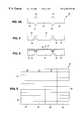
- FIG. 1Aillustrates a plastic card before a magnetic strip is affixed thereto.
- FIG. 1Billustrates the plastic card of FIG. 1A after the magnetic strip is affixed thereto.
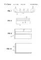
- FIG. 2illustrates in plan view a thin glass sheet after it has been subjected to laser scribing to define glass strips affixed to a glass frame.
- FIG. 2Aillustrates in cross section a portion of the glass sheet of FIG. 2 along lines A—A after laser scribing has occurred.
- FIG. 3illustrates in cross section the portion of the glass sheet of FIGS. 2 and 2A along lines A—A after it has been subjected to etching.
- FIG. 4illustrates in cross section the glass sheet of FIGS. 2 and 2A along lines A—A after an underlayer, magnetic layer and protective overcoat have been sputtered onto the glass sheet.
- FIG. 5illustrates in plan view a glass sheet after scribing in accordance with another embodiment of the invention in which the glass strips are not affixed to a frame.
- FIG. 6Aillustrates in plan view a glass sheet after it has been laser scribed in accordance with another embodiment of the invention.
- FIG. 6Bthe glass sheet of FIG. 6A after it has been etched.
- FIG. 7illustrates a glass tape being fed through sputtering apparatus.
- FIG. 8illustrates in cross section a metal foil coated with an underlayer, a magnetic layer and a protective overcoat.
- FIG. 9illustrates a card comprising a magnetic strip wherein there is no notch cut into the card prior to applying the strip.
- FIG. 10illustrates a card comprising a magnetic strip in which the strip covers an entire surface of the card.
- FIG. 11illustrates a card comprising a magnetic strip in which strips are applied to both major surfaces of the card.
- FIG. 12illustrates a card in which a strip covers an entire surface of the card, but magnetic material is provided on only a portion of the strip.
- FIG. 13illustrates a strip passing by a sputtering target in which means are provided for ensuring that magnetic material is deposited on only a portion of the strip.
- FIGS. 14A and 14Billustrate a lift-off process during which magnetic material is provided on a first portion of a strip but not a second portion.
- a method in accordance with the inventionbegins with the step of providing a thin, flexible substrate, depositing a magnetic film on the thin, flexible substrate, and applying the thin flexible substrate to a credit card type device.
- the thin, flexible substratecan be used in a high temperature sputtering process without melting, decomposing, or otherwise changing in a detrimental way. Further, the flexible substrate does not outgas contaminants during sputtering.
- the substrateAfter depositing a magnetic thin film on the flexible substrate, the substrate is cut into strips, each strip having a magnetic film thereon. The strip is then affixed to a plastic card.
- FIG. 1Aillustrates a plastic card 10 for use during a method in accordance with the invention prior to affixing a magnetic strip to card 10 .
- Card 10is typically made from a plastic material such as PVC, PTEG, or PVCA.
- Card 10is typically the size of a credit card, i.e. 3.370 inches long (85.6 mm), 2.125 inches wide (53.97 mm) and 0.030 inches thick (0.76 mm). However, these dimensions are merely exemplary, and other sizes can also be used.
- An indentation or notch 12is formed in card 10 where a magnetic strip will be placed. Indentation 12 is typically between 10 and 25 mm wide, and about 0.3 mm deep. (Card 10 is typically about 0.76 mm thick.) As explained below, a magnetic strip is affixed to card 10 at indentation 12 .
- a first embodiment of a method for making the magnetic stripcomprises the step of providing a sheet 20 of thin glass (FIG. 2 ).
- Sheet 20can be a borosilicate or aluminosilicate glass or other type of silica-containing glass.
- sheet 20can be a glass ceramic sheet.
- sheet 20is in the form of a square about 6.75 inches by 6.75 inches (171.45 mm by 171.45 mm), and about 0.3 mm or less thick. Sheet 20 can be formed by the float method or down drawing.
- Sheet 20is subjected to a laser scribing step during which a laser, such as a C 0 2 laser, is used to form scribe lines, e.g. lines 22 .
- a lasersuch as a C 0 2 laser
- the laser beamhas a wavelength that is readily absorbed by glass.
- FIG. 2Ashows some of the laser scribe lines in cross section along lines A—A. As can be seen, application of the laser to glass sheet 20 results in the formation of ridges 24 .
- Scribe lines 22are used to define rectangular strips 26 . Strips 26 are eventually separated, and affixed to card 10 .
- Glass sheet 20is then subjected to an etching process.
- This etching processis typically performed using an aqueous acidic fluorine-containing solution.
- the solutioncomprises hydrofluoric acid.
- the solutioncomprises ammonium bifluoride mixed with phosphoric acid, sulfuric acid, or other type of acid and surfactant.
- the etching solutioncomprises 5 wt. % ammonium bifluoride and 5% by volume of H 2 SO 4 .
- the surfactantcan be toluene sulfonic acid, e.g. sold as Eltesol TSX/A, manufactured by Albright & Wilson Corp.
- the etching solutionis subjected to ultrasonic agitation, e.g. at a frequency between 28 KHz and 68 KHz, e.g. 40 KHz.
- the etching solutioncan be at room temperature.
- the etching solutioncan be as described in U.S. patent application Ser. No. 09/391,140, filed Sep. 7, 1999 by Homola et al., or U.S. patent application Ser. No. 09/390,887, filed Sep. 7, 1999 by Homola.
- the '140 and '887 applicationsare incorporated herein by reference.
- the portions of glass sheet 20 subjected to the laser beametch more rapidly than the other portions of glass sheet 20 .
- FIG. 3illustrates in cross section glass sheet 20 along lines A—A after this process has been completed.
- sheet 20comprises a frame portion 29 coupled to a set of glass rectangular strips 26 via thinned glass regions 30 where scribe lines 22 were formed.
- glass sheet 20When glass sheet 20 is formed by the float method, some tin may diffuse into the glass sheet.
- a second etching stepis performed on glass sheet 20 during which the portions of glass sheet 20 that contain tin are etched away. (This etching step also strengthens glass sheet 20 by removing portions of the glass that contain defects and microcracks.) After etching, glass sheet 20 is cleaned.
- hard particlesare applied to glass sheet 20 , e.g. alumina, silica, diamond-like carbon or zirconia particles.
- the hard particlescan be provided by a dip process, spray process, or a spinning on process.
- the particlesare suspended in a liquid which, after drying, cause the particles to adhere to the glass.
- These particlesprovide enhanced mechanical support for a magnetic head that will subsequently pass over the magnetic layer. (Without adequate support, the head can eventually abrade or wear down the magnetic layer.)
- these materialscan be sputtered onto glass sheet 20 .
- the zirconiacan be stabilized, e.g. with yttria.
- Sheet 20is then mounted on a backing plate or pallet (not shown) and subjected to a sputtering process during which an underlayer 32 , magnetic layer 34 and protective overcoat 36 are deposited, e.g. by sputtering, on sheet 20 .
- the pallet or backing platecarries sheet 20 past sputtering targets that form layers 32 , 34 and 36 .
- the underlayeris a material such as Cr or a Cr alloy. Of importance, Cr or a Cr alloy enhances certain magnetic characteristics, e.g. the coercivity, of the magnetic layer 34 .
- Magnetic layer 34is typically a Co or Fe alloy.
- magnetic layer 34can comprise other materials, such as Pt, which raises the coercivity of the magnetic layer and Cr which helps prevent corrosion.
- magnetic layer 34is a CoCrPtTaB alloy.
- Protective overcoat 36can be, for example, a ceramic material such as ZrO 2 (or Y 2 O 3 -stabilized ZrO 2 ), a carbon overcoat, or a hydrogenated carbon overcoat.
- Glass sheet 20is typically heated, e.g. between 150 and 300° C. or higher during or immediately prior to sputtering. In one embodiment, sputtering is performed at 350° C. Sputtering at a high deposition temperature permits one to achieve higher magnetic coercivity. Of importance, glass is able to withstand such deposition temperatures without decomposing.
- sheet 20is heated to a temperature just below the softening point of the sheet 20 material (e.g. about 600° C.).
- a lubricant layeris applied to the protective overcoat.
- the lubricantis a “bonded” lubricant such as a perfluoropolyether lubricant.
- a portion of the perfluoropolyether lubricant moleculesbond to the protective overcoat.
- This lubricantis typically applied by dipping, spraying or wiping the lubricant onto the protective layer, followed by a bonding process (e.g. a heating or UV exposure process).
- a solid lubricante.g. graphite, MoS 2 or WS 2 , is applied in a conventional manner to protective overcoat 36 .
- the individual rectangular strips 26are separated from frame 29 . This can be accomplished by applying mechanical force to strips 26 and frame 29 . Separating strips 26 from frame 29 can also be accomplished by applying differential heating and/or cooling to frame 29 relative to strips 26 to thereby cause thermal stress and breaking along thinned regions 30 .
- strips 26are affixed to a plastic card 10 in indentation 12 using a suitable adhesive or other bonding technique. After affixing the magnetic strip to the card, the magnetic strip is tested to ensure that it performs adequately.
- glassis usually a very rigid material, whereas card 10 must be flexible and capable of bending. However, if glass strips 26 are sufficiently thin (e.g. 0.3 mm or less), they will also be flexible. Thus, using glass as a substrate to make a magnetic strip is somewhat counterintuitive.
- glass ceramiccan also be used.
- ceramic materialssuch titanium carbide, aluminum boron carbide, and boron carbide can be used.
- the glass strip or sheetincludes a texture layer formed thereon prior to deposition of underlayer 32 .
- a texture layerformed thereon prior to deposition of underlayer 32 .
- One way of doing thisis to deposit a material such as a nickel alloy, e.g. NiP, on glass sheet 20 by sputtering and then mechanically forming linear texture marks on the NiP in the longitudinal direction of glass strips 26 .
- underlayer 32 , magnetic layer 34 and protective overcoat 36are sputtered onto the textured NiP.
- a materialsuch as a nickel alloy, e.g. NiP
- underlayer 32 , magnetic layer 34 and protective overcoat 36are sputtered onto the textured NiP.
- this longitudinal texturein combination with a high temperature sputtering process that uses a Cr or Cr alloy underlayer, one can form an anisotropic magnetic film that permits higher magnetic recording density. This is achieved because magnetic coercivity is enhanced in the longitudinal direction of strip 26 .
- the linear texture markscan be formed using a laser exposure and etching technique, e.g. as described in U.S. patent application Ser. No. 09/390,887, filed by Homola on Sep. 7, 1999.
- the NiPcan be laser zone textured. In other words, one applies laser pulses to the NiP to form texture bumps. Such texture bumps can reduce friction or stiction between the magnetic strip and apparatus used to read data recorded in the magnetic strip.
- a Cr or Cr alloy underlayeris deposited on glass strip 26 .
- a CoCrTa layeris deposited on the underlayer.
- a magnetic alloy such as CoCrPtTaBis sputtered onto the CoCrTa layer.
- a protective overcoatis then deposited onto the magnetic alloy layer.
- the CoCrTa layerfacilitates improved orientation of the grains of the magnetic alloy layer, and permits better lattice matching.
- These layerscan be formed with a process such as described in U.S. patent application Ser. No. 08/984,753, filed by Bertero et al. on Dec. 4, 1997, incorporated herein by reference.
- an amorphous layersuch as sputtered NiP alloy, a magnetic alloy, and a protective overcoat are sputtered onto glass sheet 20 at a low temperature (e.g. less than about 150° C., and generally between room temperature and 150° C.).
- a low temperaturee.g. less than about 150° C., and generally between room temperature and 150° C.
- the NiP alloycan include alumina.
- Such low temperature sputtering processesgenerally produce an isotropic magnetic film. In other words, the magnetic characteristics of the film are the same in any in plane direction.
- the fifth embodimentis the same as the above embodiments, except the magnetic strips are separated from frame 29 prior to lubrication instead of after lubrication.
- frame 29is dispensed with, and glass sheet 20 ′ is formed into a set of strips 26 ′ which are connected to one another.
- One advantage of this methodis that more strips can be formed on a sheet, since there is no frame.
- glass sheet 20is laser scribed so that laser scribe line 22 ′′ completely surrounds strips 26 ′′ except at regions 38 .
- Sheet 20 ′′is then subjected to an etching process so that portions of the glass surrounding strips 26 ′′ are completely removed except for portions of glass which form tabs 40 (FIG. 6 B). (Tabs 40 are located where regions 38 were previously located.) Strips 26 ′′ are held to frame 29 ′′ via tabs 40 .
- strips 26 ′′are separated from frame 29 ′′ by breaking tabs 40 . Strips 26 ′′ are then affixed to card 10 as described above.
- strips 26 ′′can be coupled to each other via tabs 40 without a frame.
- a long, thin glass tape 41 from a supply reel 42is passed underneath sputtering targets 43 , 44 and 46 , and is then taken up on a take-up reel 48 .
- Targets 43 , 44 and 46provide an underlayer, a magnetic layer and a protective overcoat.
- reel 48is removed from the sputtering apparatus, and tape 41 is cut into individual strips to be mounted onto card 10 .
- tape 41is mechanically cut into strips after sputtering.
- scribe linesare formed in tape 41 so that tape 41 can easily be separated into strips after sputtering.
- tape 41is laser scribed and etched to form thinned regions so that the tape can easily be separated into strips after sputtering.
- a thin metal foil 60 mounted on a pallet or backing plateis introduced into sputtering apparatus.
- Foil 60can be Cu, Be, W, Ti, Ta, brass, stainless steel or other appropriate metal, and is typically 0.3 mm thick or less.
- Foil 60is flexible.
- An underlayer 64 , a magnetic alloy 66 and a protective overcoat 68are deposited on thin metal foil 60 in that order.
- the underlayercan comprise a material such as Cr or a Cr alloy, NiAl or NiP.
- the magnetic alloyis typically a Co or Fe alloy.
- the protective overcoatcan be a ceramic material or carbon.
- a lubricantis then applied to protective overcoat 68 .
- Foil 60is then cut, e.g. using a laser, EDM apparatus (electrical discharge machinery) or other appropriate cutting technique. Thereafter, coated foil 60 is affixed to card 10 , e.g. using an adhesive. The card may then be tested, as in other embodiments.
- foil 60can be in the form of a strip provided on a reel such as reel 42 , and can be passed under sputtering targets in a manner similar to glass tape 41 described above in conjunction with FIG. 7 .
- notch 12is formed in card 10 .
- notch 12is not formed in card 10 .
- strip 26is simply affixed to card 10 , e.g. as shown in FIG. 9 .
- a notchis formed on each side of card 10 , and a magnetic strip is affixed to each notch.
- strip 26is dimensioned so as to cover approximately one entire surface of card 10 , e.g. as shown in FIG. 10 .
- more datacan be stored on the strip because it is larger.
- strip 26is dimensioned to cover an entire surface of card 10 , and another strip 26 a is applied to the other surface of card 10 (FIG. 11 ).
- Strip 26 amay or may not have magnetic layers formed thereon, but in either case is preferably made from the same material as the substrate of strip 26 (e.g. glass).
- the cardis mechanically more symmetrical and therefore more reliable.
- strip 26 ais transparent, one can read information printed on card 10 through strip 26 a.
- strip 26is dimensioned to cover the entire surface of card 10 , but only a portion 26 b of strip 26 has any layers sputtered thereon (FIG. 12 ).
- the other portions 26 c of strip 26do not have any layers sputtered thereon.
- One advantage of this embodimentis that one does not have to cut a notch in card 10 , but nonetheless the surface of card 10 is smooth.
- Another advantage of this embodimentis that if the substrate material of strip 26 is transparent (e.g. glass), one can read information printed on the surface of card 10 that is covered by portions 26 c of strip 26 .
- the sputtered layerscan be confined to portion 26 b of strip 26 in one of the following ways.
- strip 26is subjected to a lithographic masking and etching process to remove those portions of the sputtered layers from portion 26 c of strip 26 .
- walls or sheets 50are interposed between the sputtering targets (e.g. target 52 ) and portions 26 c of strip 26 as strip 26 moves in the direction of arrow 53 past the targets (FIG. 13 ). These walls or sheets block sputtered material from landing on and adhering to portions 26 c of strip 26 . Accordingly, when strip 26 emerges from the sputtering process, the sputtered layers are confined to portion 26 b.
- a resist layer 54can be applied to strip 26 and exposed, and the portion of resist on portion 26 b of strip 26 is removed. (See FIG. 14A, which illustrates a portion of strip 16 in cross section with resist layer 54 formed thereon.) Thereafter, underlayer 32 , magnetic layer 34 and overcoat 36 are sputtered onto strip 26 . After sputtering, the remaining portions of the resist 54 are removed, along with any sputtered layers on the resist. The result of this method is that sputtered layers are only present on portion 26 b and not on portion 26 c of strip 26 .
- the card and substrate materialscan be any appropriate size or thickness.
- sputtering, evaporation, ion plating, or other vacuum deposition techniquescan be used.
- notch 12does not span the entire length of the card.
- the sheetcan be cut mechanically after sputtering in lieu of scribing and breaking along the scribe lines.
- glass sheet 20is laser scribed but not etched after laser scribing.
- the various layersare deposited (e.g. by sputtering) onto sheet 20 , and then the magnetic strips are separated from frame 29 along the laser scribe lines, e.g. mechanically or by applying thermal stress along the laser scribe lines.
- scribing and etching of glass sheet 20is accomplished after sputtering the various layers thereon. In yet another embodiment, scribing is performed after the various layers are sputtered onto glass sheet 20 . The glass sheet is broken into strips without the above-mentioned etching step. Accordingly, all such changes come within the present invention.
Landscapes
- Physics & Mathematics (AREA)
- General Physics & Mathematics (AREA)
- Engineering & Computer Science (AREA)
- Theoretical Computer Science (AREA)
- Manufacturing Of Magnetic Record Carriers (AREA)
Abstract
Description
Claims (46)
Priority Applications (3)
| Application Number | Priority Date | Filing Date | Title |
|---|---|---|---|
| US09/410,679US6482330B1 (en) | 1999-10-01 | 1999-10-01 | Method for manufacturing a data storage card |
| PCT/US2000/026909WO2001026030A2 (en) | 1999-10-01 | 2000-09-29 | Method for manufacturing a data storage card |
| AU76238/00AAU7623800A (en) | 1999-10-01 | 2000-09-29 | Method for manufacturing a data storage card |
Applications Claiming Priority (1)
| Application Number | Priority Date | Filing Date | Title |
|---|---|---|---|
| US09/410,679US6482330B1 (en) | 1999-10-01 | 1999-10-01 | Method for manufacturing a data storage card |
Publications (1)
| Publication Number | Publication Date |
|---|---|
| US6482330B1true US6482330B1 (en) | 2002-11-19 |
Family
ID=23625762
Family Applications (1)
| Application Number | Title | Priority Date | Filing Date |
|---|---|---|---|
| US09/410,679Expired - LifetimeUS6482330B1 (en) | 1999-10-01 | 1999-10-01 | Method for manufacturing a data storage card |
Country Status (3)
| Country | Link |
|---|---|
| US (1) | US6482330B1 (en) |
| AU (1) | AU7623800A (en) |
| WO (1) | WO2001026030A2 (en) |
Cited By (84)
| Publication number | Priority date | Publication date | Assignee | Title |
|---|---|---|---|---|
| US20010055702A1 (en)* | 2000-05-12 | 2001-12-27 | Wang Po Wen | Self-lubricating layer for data storage devices |
| USD509847S1 (en)* | 2001-12-14 | 2005-09-20 | Ultracard, Inc. | Removable and reinsertable strip storage member for a credit card |
| US20050282046A1 (en)* | 2004-06-22 | 2005-12-22 | Imation Corp. | Magnetic recording medium having a dimensionally stable substrate |
| US20060102729A1 (en)* | 2003-01-03 | 2006-05-18 | Priscilla Gandel | Metal-containing transaction card and method of making the same |
| US20070170264A1 (en)* | 2003-01-03 | 2007-07-26 | Ellen Lasch | Metal-containing transaction card and method of making the same |
| US20080314995A1 (en)* | 2003-01-03 | 2008-12-25 | American Express Travel Related Services Company, Inc. | Metal-containing transaction card and method of making same |
| US7487908B1 (en) | 1999-10-23 | 2009-02-10 | Ultracard, Inc. | Article having an embedded accessible storage member, apparatus and method for using same |
| USD602986S1 (en) | 2009-03-06 | 2009-10-27 | Jpmorgan Chase Bank, N.A. | Metal transaction device |
| US7702538B2 (en) | 2000-08-01 | 2010-04-20 | Jpmorgan Chase Bank, N.A. | System and method for transponder-enabled account transactions |
| USD635186S1 (en) | 2008-06-30 | 2011-03-29 | Jpmorgan Chase Bank, N.A. | Metal transaction device |
| USD636021S1 (en) | 2008-07-17 | 2011-04-12 | Jpmorgan Chase Bank, N.A. | Eco-friendly transaction device |
| US20110097603A1 (en)* | 2008-03-26 | 2011-04-28 | Wd Media (Singapore) Pte. Ltd. | Perpendicular magnetic recording medium and process for manufacture thereof |
| US20110097604A1 (en)* | 2008-03-31 | 2011-04-28 | Wd Media (Singapore) Pte. Ltd. | Perpendicular magnetic recording medium |
| US20110171495A1 (en)* | 2010-01-08 | 2011-07-14 | Wd Media (Singapore) Pte. Ltd. | Perpendicular magnetic recording medium |
| US8033457B2 (en) | 2003-01-03 | 2011-10-11 | American Express Travel Related Services Company, Inc. | Metal-containing transaction card and method of making the same |
| US8397998B1 (en)* | 1999-10-23 | 2013-03-19 | Ultracard, Inc. | Data storage device, apparatus and method for using same |
| US8828566B2 (en) | 2010-05-21 | 2014-09-09 | Wd Media (Singapore) Pte. Ltd. | Perpendicular magnetic recording disc |
| US8867322B1 (en) | 2013-05-07 | 2014-10-21 | WD Media, LLC | Systems and methods for providing thermal barrier bilayers for heat assisted magnetic recording media |
| US8877359B2 (en) | 2008-12-05 | 2014-11-04 | Wd Media (Singapore) Pte. Ltd. | Magnetic disk and method for manufacturing same |
| US8908315B2 (en) | 2010-03-29 | 2014-12-09 | Wd Media (Singapore) Pte. Ltd. | Evaluation method of magnetic disk, manufacturing method of magnetic disk, and magnetic disk |
| US8941950B2 (en) | 2012-05-23 | 2015-01-27 | WD Media, LLC | Underlayers for heat assisted magnetic recording (HAMR) media |
| US8947987B1 (en) | 2013-05-03 | 2015-02-03 | WD Media, LLC | Systems and methods for providing capping layers for heat assisted magnetic recording media |
| US8951651B2 (en) | 2010-05-28 | 2015-02-10 | Wd Media (Singapore) Pte. Ltd. | Perpendicular magnetic recording disk |
| US8980076B1 (en) | 2009-05-26 | 2015-03-17 | WD Media, LLC | Electro-deposited passivation coatings for patterned media |
| US8995078B1 (en) | 2014-09-25 | 2015-03-31 | WD Media, LLC | Method of testing a head for contamination |
| US8993134B2 (en) | 2012-06-29 | 2015-03-31 | Western Digital Technologies, Inc. | Electrically conductive underlayer to grow FePt granular media with (001) texture on glass substrates |
| US9001630B1 (en) | 2011-03-08 | 2015-04-07 | Western Digital Technologies, Inc. | Energy assisted magnetic recording medium capable of suppressing high DC readback noise |
| US9005782B2 (en) | 2008-03-30 | 2015-04-14 | WD Media, LLC | Magnetic disk and method of manufacturing the same |
| US9025264B1 (en) | 2011-03-10 | 2015-05-05 | WD Media, LLC | Methods for measuring media performance associated with adjacent track interference |
| US9028985B2 (en) | 2011-03-31 | 2015-05-12 | WD Media, LLC | Recording media with multiple exchange coupled magnetic layers |
| US9029308B1 (en) | 2012-03-28 | 2015-05-12 | WD Media, LLC | Low foam media cleaning detergent |
| US9034492B1 (en) | 2013-01-11 | 2015-05-19 | WD Media, LLC | Systems and methods for controlling damping of magnetic media for heat assisted magnetic recording |
| US9042053B1 (en) | 2014-06-24 | 2015-05-26 | WD Media, LLC | Thermally stabilized perpendicular magnetic recording medium |
| US9047880B1 (en) | 2011-12-20 | 2015-06-02 | WD Media, LLC | Heat assisted magnetic recording method for media having moment keeper layer |
| US9064521B1 (en) | 2011-03-25 | 2015-06-23 | WD Media, LLC | Manufacturing of hard masks for patterning magnetic media |
| US9082447B1 (en) | 2014-09-22 | 2015-07-14 | WD Media, LLC | Determining storage media substrate material type |
| US9093100B2 (en) | 2008-03-17 | 2015-07-28 | Wd Media (Singapore) Pte. Ltd. | Magnetic recording medium including tailored exchange coupling layer and manufacturing method of the same |
| US9093122B1 (en) | 2013-04-05 | 2015-07-28 | WD Media, LLC | Systems and methods for improving accuracy of test measurements involving aggressor tracks written to disks of hard disk drives |
| US9142241B2 (en) | 2009-03-30 | 2015-09-22 | Wd Media (Singapore) Pte. Ltd. | Perpendicular magnetic recording medium and method of manufacturing the same |
| US9153268B1 (en) | 2013-02-19 | 2015-10-06 | WD Media, LLC | Lubricants comprising fluorinated graphene nanoribbons for magnetic recording media structure |
| US9159350B1 (en) | 2014-07-02 | 2015-10-13 | WD Media, LLC | High damping cap layer for magnetic recording media |
| US9177586B2 (en) | 2008-09-30 | 2015-11-03 | WD Media (Singapore), LLC | Magnetic disk and manufacturing method thereof |
| US9177585B1 (en) | 2013-10-23 | 2015-11-03 | WD Media, LLC | Magnetic media capable of improving magnetic properties and thermal management for heat-assisted magnetic recording |
| US9183867B1 (en) | 2013-02-21 | 2015-11-10 | WD Media, LLC | Systems and methods for forming implanted capping layers in magnetic media for magnetic recording |
| US9190094B2 (en) | 2013-04-04 | 2015-11-17 | Western Digital (Fremont) | Perpendicular recording media with grain isolation initiation layer and exchange breaking layer for signal-to-noise ratio enhancement |
| US9196283B1 (en) | 2013-03-13 | 2015-11-24 | Western Digital (Fremont), Llc | Method for providing a magnetic recording transducer using a chemical buffer |
| US9218850B1 (en) | 2014-12-23 | 2015-12-22 | WD Media, LLC | Exchange break layer for heat-assisted magnetic recording media |
| US9227324B1 (en) | 2014-09-25 | 2016-01-05 | WD Media, LLC | Mandrel for substrate transport system with notch |
| US9240204B2 (en) | 2010-05-21 | 2016-01-19 | Wd Media (Singapore) Pte. Ltd. | Perpendicular magnetic recording disc |
| US9257134B1 (en) | 2014-12-24 | 2016-02-09 | Western Digital Technologies, Inc. | Allowing fast data zone switches on data storage devices |
| US9269480B1 (en) | 2012-03-30 | 2016-02-23 | WD Media, LLC | Systems and methods for forming magnetic recording media with improved grain columnar growth for energy assisted magnetic recording |
| US9275669B1 (en) | 2015-03-31 | 2016-03-01 | WD Media, LLC | TbFeCo in PMR media for SNR improvement |
| US9280998B1 (en) | 2015-03-30 | 2016-03-08 | WD Media, LLC | Acidic post-sputter wash for magnetic recording media |
| US9296082B1 (en) | 2013-06-11 | 2016-03-29 | WD Media, LLC | Disk buffing apparatus with abrasive tape loading pad having a vibration absorbing layer |
| US9305292B1 (en) | 2008-07-03 | 2016-04-05 | Jpmorgan Chase Bank, N.A. | Systems and methods for providing an adaptable transponder device |
| US9330685B1 (en) | 2009-11-06 | 2016-05-03 | WD Media, LLC | Press system for nano-imprinting of recording media with a two step pressing method |
| US9339978B1 (en) | 2009-11-06 | 2016-05-17 | WD Media, LLC | Press system with interleaved embossing foil holders for nano-imprinting of recording media |
| US9349404B2 (en) | 2010-05-28 | 2016-05-24 | Wd Media (Singapore) Pte. Ltd | Perpendicular magnetic recording disc |
| US9382496B1 (en) | 2013-12-19 | 2016-07-05 | Western Digital Technologies, Inc. | Lubricants with high thermal stability for heat-assisted magnetic recording |
| US9389135B2 (en) | 2013-09-26 | 2016-07-12 | WD Media, LLC | Systems and methods for calibrating a load cell of a disk burnishing machine |
| US9401300B1 (en) | 2014-12-18 | 2016-07-26 | WD Media, LLC | Media substrate gripper including a plurality of snap-fit fingers |
| US9406330B1 (en) | 2013-06-19 | 2016-08-02 | WD Media, LLC | Method for HDD disk defect source detection |
| US9406329B1 (en) | 2015-11-30 | 2016-08-02 | WD Media, LLC | HAMR media structure with intermediate layer underlying a magnetic recording layer having multiple sublayers |
| US9431045B1 (en) | 2014-04-25 | 2016-08-30 | WD Media, LLC | Magnetic seed layer used with an unbalanced soft underlayer |
| US9449633B1 (en) | 2014-11-06 | 2016-09-20 | WD Media, LLC | Smooth structures for heat-assisted magnetic recording media |
| US9447368B1 (en) | 2014-02-18 | 2016-09-20 | WD Media, LLC | Detergent composition with low foam and high nickel solubility |
| US9472227B2 (en) | 2010-06-22 | 2016-10-18 | Wd Media (Singapore) Pte. Ltd. | Perpendicular magnetic recording media and methods for producing the same |
| US9542968B1 (en) | 2010-08-20 | 2017-01-10 | WD Media, LLC | Single layer small grain size FePT:C film for heat assisted magnetic recording media |
| US9558778B2 (en) | 2009-03-28 | 2017-01-31 | Wd Media (Singapore) Pte. Ltd. | Lubricant compound for magnetic disk and magnetic disk |
| US9581510B1 (en) | 2013-12-16 | 2017-02-28 | Western Digital Technologies, Inc. | Sputter chamber pressure gauge with vibration absorber |
| US9607646B2 (en) | 2013-07-30 | 2017-03-28 | WD Media, LLC | Hard disk double lubrication layer |
| US9685184B1 (en) | 2014-09-25 | 2017-06-20 | WD Media, LLC | NiFeX-based seed layer for magnetic recording media |
| US9818442B2 (en) | 2014-12-01 | 2017-11-14 | WD Media, LLC | Magnetic media having improved magnetic grain size distribution and intergranular segregation |
| US9822441B2 (en) | 2015-03-31 | 2017-11-21 | WD Media, LLC | Iridium underlayer for heat assisted magnetic recording media |
| US9824711B1 (en) | 2014-02-14 | 2017-11-21 | WD Media, LLC | Soft underlayer for heat assisted magnetic recording media |
| US9990940B1 (en) | 2014-12-30 | 2018-06-05 | WD Media, LLC | Seed structure for perpendicular magnetic recording media |
| US10054363B2 (en) | 2014-08-15 | 2018-08-21 | WD Media, LLC | Method and apparatus for cryogenic dynamic cooling |
| US10083715B2 (en) | 2010-05-28 | 2018-09-25 | WD Media (Singapore) Pte.Ltd. | Method of manufacturing a perpendicular magnetic disc |
| US10115428B1 (en) | 2013-02-15 | 2018-10-30 | Wd Media, Inc. | HAMR media structure having an anisotropic thermal barrier layer |
| US10121506B1 (en) | 2015-12-29 | 2018-11-06 | WD Media, LLC | Magnetic-recording medium including a carbon overcoat implanted with nitrogen and hydrogen |
| US10236026B1 (en) | 2015-11-06 | 2019-03-19 | WD Media, LLC | Thermal barrier layers and seed layers for control of thermal and structural properties of HAMR media |
| US10607125B2 (en) | 2015-02-06 | 2020-03-31 | American Express Travel Related Services Company, Inc. | Method of making ceramic-containing transaction cards |
| US11074934B1 (en) | 2015-09-25 | 2021-07-27 | Western Digital Technologies, Inc. | Heat assisted magnetic recording (HAMR) media with Curie temperature reduction layer |
| US20240403592A1 (en)* | 2014-05-22 | 2024-12-05 | Composecure, Llc | Transaction and id cards having selected texture and coloring |
Families Citing this family (2)
| Publication number | Priority date | Publication date | Assignee | Title |
|---|---|---|---|---|
| DE102010019615A1 (en)* | 2010-05-06 | 2011-11-10 | Rat Asset & Trading Ag | Card for electronic access control |
| EP4354341A1 (en)* | 2022-10-10 | 2024-04-17 | Giesecke+Devrient ePayments GmbH | Methods for manufacturing a magnetic stripe of a card-like data carrier |
Citations (30)
| Publication number | Priority date | Publication date | Assignee | Title |
|---|---|---|---|---|
| US3808404A (en) | 1971-12-29 | 1974-04-30 | Magneguide Corp | Magnetic identification card |
| US4002804A (en) | 1974-07-31 | 1977-01-11 | Fuji Photo Film Co., Ltd. | Magnetic recording material |
| US4066873A (en) | 1976-01-26 | 1978-01-03 | The First National Bank Of Chicago | Identification and access card with associated optical decoding means |
| US4100011A (en) | 1975-08-04 | 1978-07-11 | Addressograph Multigraph Corp. | Production of laminated card with printed magnetically encodable stripe |
| US4197988A (en) | 1977-12-02 | 1980-04-15 | The Vendo Company | Apparatus for reading and writing data onto a magnetic stripe and in an arcuate path |
| US4325182A (en)* | 1980-08-25 | 1982-04-20 | General Electric Company | Fast isolation diffusion |
| EP0106533A2 (en) | 1982-09-13 | 1984-04-25 | Applied Magnetics Magnetic Head Division Corporation | Magnetic head assembly having improved read/write characteristics for a floppy disc |
| US4592042A (en) | 1983-02-16 | 1986-05-27 | Lemelson Jerome H | Record card transducing apparatus and method |
| US4707593A (en) | 1985-05-29 | 1987-11-17 | Pilot Man-Nen-Hitsu Kabushiki Kaisha | Visible image magnetic card |
| US4742410A (en) | 1983-12-16 | 1988-05-03 | Josephine County Technology, Inc. | Disk drive system with head protection mechanism |
| US4788156A (en) | 1986-09-24 | 1988-11-29 | Microwave Technology, Inc. | Subchannel doping to reduce short-gate effects in field effect transistors |
| US4863546A (en) | 1983-07-01 | 1989-09-05 | Roland Melzer | Apparatus and method for manufacturing plastic cards |
| US4871523A (en) | 1987-05-15 | 1989-10-03 | Exxon Chemical Patents Inc. | Vanadium tetrachloride stabilization |
| US4938830A (en) | 1988-03-07 | 1990-07-03 | Perfect Plastic Printing Corp. | Plastic card and method of fabrication thereof |
| US5047296A (en)* | 1987-09-18 | 1991-09-10 | Commissariat A L'energie Atomique | Composite magnetic material and its production process |
| EP0451024A1 (en) | 1990-04-02 | 1991-10-09 | Gemplus Card International | Security card combining a high density information carrier and a microcircuit, and method for use in a card reader |
| US5087481A (en)* | 1986-10-09 | 1992-02-11 | Komag, Inc. | Method for texturing a magnetic disk silicate glass substrate |
| US5107099A (en) | 1989-04-24 | 1992-04-21 | Smith Malcolm G | Magnetic card reader and method |
| US5395672A (en)* | 1988-10-18 | 1995-03-07 | Kiota | Large-capacity magnetic memory card and manufacturing method |
| US5435878A (en) | 1988-10-18 | 1995-07-25 | Gemplus S.C.A. | Method for welding polycarbonate by high frequency |
| WO1996011098A1 (en) | 1994-10-06 | 1996-04-18 | Perstorp Ab | Process of incorporating a unit or object by moulding |
| US5530232A (en) | 1993-12-22 | 1996-06-25 | Datamark Services, Inc. | Multi-application data card |
| US5534324A (en)* | 1992-11-12 | 1996-07-09 | Matsushita Electric Industrial Co., Ltd. | Magnetic recording medium and method for producing the same |
| US5567537A (en)* | 1994-04-11 | 1996-10-22 | Hitachi Metals, Ltd. | Magnetic core element for antenna, thin-film antenna, and card equipped with thin-film antenna |
| US5612403A (en) | 1990-10-24 | 1997-03-18 | Johnson Matthey, Inc. | Low temperature flexible die attach adhesive and articles using same |
| DE19601176A1 (en) | 1996-01-15 | 1997-07-24 | Ibm | Smart card reader with floppy disc shape for floppy disc drive |
| EP0833282A1 (en) | 1996-09-30 | 1998-04-01 | Fontaine S.A. | Electronic card reader for controlling a lock |
| DE29804131U1 (en) | 1998-03-09 | 1998-06-25 | Kastrop, Norbert, 30827 Garbsen | Multipurpose card |
| US5844230A (en)* | 1993-08-09 | 1998-12-01 | Lalonde; Michael G. | Information card |
| US6288870B1 (en)* | 1998-01-13 | 2001-09-11 | Quantum Corporation | Self-aligned metal film core multi-channel recording head for tape drives |
- 1999
- 1999-10-01USUS09/410,679patent/US6482330B1/ennot_activeExpired - Lifetime
- 2000
- 2000-09-29WOPCT/US2000/026909patent/WO2001026030A2/enactiveApplication Filing
- 2000-09-29AUAU76238/00Apatent/AU7623800A/ennot_activeAbandoned
Patent Citations (30)
| Publication number | Priority date | Publication date | Assignee | Title |
|---|---|---|---|---|
| US3808404A (en) | 1971-12-29 | 1974-04-30 | Magneguide Corp | Magnetic identification card |
| US4002804A (en) | 1974-07-31 | 1977-01-11 | Fuji Photo Film Co., Ltd. | Magnetic recording material |
| US4100011A (en) | 1975-08-04 | 1978-07-11 | Addressograph Multigraph Corp. | Production of laminated card with printed magnetically encodable stripe |
| US4066873A (en) | 1976-01-26 | 1978-01-03 | The First National Bank Of Chicago | Identification and access card with associated optical decoding means |
| US4197988A (en) | 1977-12-02 | 1980-04-15 | The Vendo Company | Apparatus for reading and writing data onto a magnetic stripe and in an arcuate path |
| US4325182A (en)* | 1980-08-25 | 1982-04-20 | General Electric Company | Fast isolation diffusion |
| EP0106533A2 (en) | 1982-09-13 | 1984-04-25 | Applied Magnetics Magnetic Head Division Corporation | Magnetic head assembly having improved read/write characteristics for a floppy disc |
| US4592042A (en) | 1983-02-16 | 1986-05-27 | Lemelson Jerome H | Record card transducing apparatus and method |
| US4863546A (en) | 1983-07-01 | 1989-09-05 | Roland Melzer | Apparatus and method for manufacturing plastic cards |
| US4742410A (en) | 1983-12-16 | 1988-05-03 | Josephine County Technology, Inc. | Disk drive system with head protection mechanism |
| US4707593A (en) | 1985-05-29 | 1987-11-17 | Pilot Man-Nen-Hitsu Kabushiki Kaisha | Visible image magnetic card |
| US4788156A (en) | 1986-09-24 | 1988-11-29 | Microwave Technology, Inc. | Subchannel doping to reduce short-gate effects in field effect transistors |
| US5087481A (en)* | 1986-10-09 | 1992-02-11 | Komag, Inc. | Method for texturing a magnetic disk silicate glass substrate |
| US4871523A (en) | 1987-05-15 | 1989-10-03 | Exxon Chemical Patents Inc. | Vanadium tetrachloride stabilization |
| US5047296A (en)* | 1987-09-18 | 1991-09-10 | Commissariat A L'energie Atomique | Composite magnetic material and its production process |
| US4938830A (en) | 1988-03-07 | 1990-07-03 | Perfect Plastic Printing Corp. | Plastic card and method of fabrication thereof |
| US5395672A (en)* | 1988-10-18 | 1995-03-07 | Kiota | Large-capacity magnetic memory card and manufacturing method |
| US5435878A (en) | 1988-10-18 | 1995-07-25 | Gemplus S.C.A. | Method for welding polycarbonate by high frequency |
| US5107099A (en) | 1989-04-24 | 1992-04-21 | Smith Malcolm G | Magnetic card reader and method |
| EP0451024A1 (en) | 1990-04-02 | 1991-10-09 | Gemplus Card International | Security card combining a high density information carrier and a microcircuit, and method for use in a card reader |
| US5612403A (en) | 1990-10-24 | 1997-03-18 | Johnson Matthey, Inc. | Low temperature flexible die attach adhesive and articles using same |
| US5534324A (en)* | 1992-11-12 | 1996-07-09 | Matsushita Electric Industrial Co., Ltd. | Magnetic recording medium and method for producing the same |
| US5844230A (en)* | 1993-08-09 | 1998-12-01 | Lalonde; Michael G. | Information card |
| US5530232A (en) | 1993-12-22 | 1996-06-25 | Datamark Services, Inc. | Multi-application data card |
| US5567537A (en)* | 1994-04-11 | 1996-10-22 | Hitachi Metals, Ltd. | Magnetic core element for antenna, thin-film antenna, and card equipped with thin-film antenna |
| WO1996011098A1 (en) | 1994-10-06 | 1996-04-18 | Perstorp Ab | Process of incorporating a unit or object by moulding |
| DE19601176A1 (en) | 1996-01-15 | 1997-07-24 | Ibm | Smart card reader with floppy disc shape for floppy disc drive |
| EP0833282A1 (en) | 1996-09-30 | 1998-04-01 | Fontaine S.A. | Electronic card reader for controlling a lock |
| US6288870B1 (en)* | 1998-01-13 | 2001-09-11 | Quantum Corporation | Self-aligned metal film core multi-channel recording head for tape drives |
| DE29804131U1 (en) | 1998-03-09 | 1998-06-25 | Kastrop, Norbert, 30827 Garbsen | Multipurpose card |
Non-Patent Citations (8)
| Title |
|---|
| "Magnetic Stripes" (3 pages). |
| "Welcome to Smart Cards", bearing a copyright notice dated 1998. |
| A. Bergeron, et al., "Structure of the Interfacial Region Between Polycarbonate and Plasma-Deposited SiN1.3 and SiO2 Optical Coatings Studied by Ellipsometry", J. Vac. Sci. Technol., vol. 16, Issue 6, pp. 3227-3234, Nov. 1998. |
| Dialog printout. |
| ICMA Quick Card Facts, bearing the date Aug. 10, 1999. |
| Magnetic Stripe Technology, bearing the date Jul. 30, 1999. |
| Morita et al., "The Durability of New Rigid Disks by Molded Plastic Substrates", J. Appl. Phys., vol. 75, Issue 10, p. 6162, May 15, 1994. |
| Smart Card Basics, bearing the date Aug. 12, 1999. |
Cited By (109)
| Publication number | Priority date | Publication date | Assignee | Title |
|---|---|---|---|---|
| US9430727B2 (en)* | 1999-10-23 | 2016-08-30 | Ultracard, Inc. | Data storage device, apparatus and method for using same |
| US8397998B1 (en)* | 1999-10-23 | 2013-03-19 | Ultracard, Inc. | Data storage device, apparatus and method for using same |
| US7487908B1 (en) | 1999-10-23 | 2009-02-10 | Ultracard, Inc. | Article having an embedded accessible storage member, apparatus and method for using same |
| US7988036B2 (en) | 1999-10-23 | 2011-08-02 | Ultracard, Inc. | Article having an embedded accessible storage member, apparatus and method for using same |
| US7988061B2 (en) | 1999-10-23 | 2011-08-02 | Ultracard, Inc. | Article having an embedded accessible storage member, apparatus and method for using same |
| US6677105B2 (en)* | 2000-05-12 | 2004-01-13 | Toda Kogyo Corporation | Self-lubricating layer for data storage devices |
| US20010055702A1 (en)* | 2000-05-12 | 2001-12-27 | Wang Po Wen | Self-lubricating layer for data storage devices |
| US7702538B2 (en) | 2000-08-01 | 2010-04-20 | Jpmorgan Chase Bank, N.A. | System and method for transponder-enabled account transactions |
| US8781904B2 (en) | 2000-08-01 | 2014-07-15 | Jpmorgan Chase Bank, N.A. | System and method for transponder-enabled account transactions |
| US8781905B2 (en) | 2000-08-01 | 2014-07-15 | Jpmorgan Chase Bank, N.A. | System and method for transponder-enabled account transactions |
| USD509847S1 (en)* | 2001-12-14 | 2005-09-20 | Ultracard, Inc. | Removable and reinsertable strip storage member for a credit card |
| US8360312B2 (en) | 2003-01-03 | 2013-01-29 | American Express Travel Releated Services Company, Inc. | Metal-containing transaction card and method of making the same |
| US20080314995A1 (en)* | 2003-01-03 | 2008-12-25 | American Express Travel Related Services Company, Inc. | Metal-containing transaction card and method of making same |
| US7588184B2 (en) | 2003-01-03 | 2009-09-15 | American Express Travel Related Services Company, Inc. | Metal-containing transaction card and method of making the same |
| US7819310B2 (en) | 2003-01-03 | 2010-10-26 | American Express Travel Related Services Company Inc. | Metal-containing transaction card and method of making the same |
| US7823777B2 (en) | 2003-01-03 | 2010-11-02 | American Express Travel Related Services Company, Inc. | Metal-containing transaction card and method of making same |
| US20060102729A1 (en)* | 2003-01-03 | 2006-05-18 | Priscilla Gandel | Metal-containing transaction card and method of making the same |
| US20070170264A1 (en)* | 2003-01-03 | 2007-07-26 | Ellen Lasch | Metal-containing transaction card and method of making the same |
| US8523062B2 (en) | 2003-01-03 | 2013-09-03 | American Express Travel Related Services Company, Inc. | Metal-containing transaction card and method of making the same |
| US8079514B2 (en) | 2003-01-03 | 2011-12-20 | American Express Travel Related Services Company, Inc. | Metal-containing transaction card and method of making the same |
| US8033457B2 (en) | 2003-01-03 | 2011-10-11 | American Express Travel Related Services Company, Inc. | Metal-containing transaction card and method of making the same |
| US7971786B2 (en) | 2003-01-03 | 2011-07-05 | American Express Travel Related Services Company, Inc. | Metal-containing transaction card and method of making the same |
| US20110226858A1 (en)* | 2003-01-03 | 2011-09-22 | American Express Travel Related Services Company, Inc. | Metal-containing transaction card and method of making the same |
| US7530491B2 (en) | 2003-01-03 | 2009-05-12 | American Express Travel Related Services Company, Inc. | Metal-containing transaction card and method of making the same |
| US7494057B2 (en)* | 2003-01-03 | 2009-02-24 | American Express Travel Related Services Company, Inc. | Metal-containing transaction card and method of making the same |
| US6989204B2 (en)* | 2004-06-22 | 2006-01-24 | Imation Corp. | Magnetic recording medium having a dimensionally stable substrate |
| US20050282046A1 (en)* | 2004-06-22 | 2005-12-22 | Imation Corp. | Magnetic recording medium having a dimensionally stable substrate |
| US9093100B2 (en) | 2008-03-17 | 2015-07-28 | Wd Media (Singapore) Pte. Ltd. | Magnetic recording medium including tailored exchange coupling layer and manufacturing method of the same |
| US20110097603A1 (en)* | 2008-03-26 | 2011-04-28 | Wd Media (Singapore) Pte. Ltd. | Perpendicular magnetic recording medium and process for manufacture thereof |
| US9047903B2 (en) | 2008-03-26 | 2015-06-02 | Wd Media (Singapore) Pte. Ltd. | Perpendicular magnetic recording medium and process for manufacture thereof |
| US9005782B2 (en) | 2008-03-30 | 2015-04-14 | WD Media, LLC | Magnetic disk and method of manufacturing the same |
| US20110097604A1 (en)* | 2008-03-31 | 2011-04-28 | Wd Media (Singapore) Pte. Ltd. | Perpendicular magnetic recording medium |
| USD635186S1 (en) | 2008-06-30 | 2011-03-29 | Jpmorgan Chase Bank, N.A. | Metal transaction device |
| USD643062S1 (en) | 2008-06-30 | 2011-08-09 | Jpmorgan Chase Bank, N.A. | Metal transaction device |
| US9305292B1 (en) | 2008-07-03 | 2016-04-05 | Jpmorgan Chase Bank, N.A. | Systems and methods for providing an adaptable transponder device |
| USD636020S1 (en) | 2008-07-17 | 2011-04-12 | Jpmorgan Chase Bank, N.A. | Eco-friendly transaction device |
| USD636021S1 (en) | 2008-07-17 | 2011-04-12 | Jpmorgan Chase Bank, N.A. | Eco-friendly transaction device |
| US9177586B2 (en) | 2008-09-30 | 2015-11-03 | WD Media (Singapore), LLC | Magnetic disk and manufacturing method thereof |
| US9984715B2 (en) | 2008-09-30 | 2018-05-29 | WD Media, LLC | Magnetic disk and manufacturing method thereof |
| US8877359B2 (en) | 2008-12-05 | 2014-11-04 | Wd Media (Singapore) Pte. Ltd. | Magnetic disk and method for manufacturing same |
| USD602986S1 (en) | 2009-03-06 | 2009-10-27 | Jpmorgan Chase Bank, N.A. | Metal transaction device |
| US9558778B2 (en) | 2009-03-28 | 2017-01-31 | Wd Media (Singapore) Pte. Ltd. | Lubricant compound for magnetic disk and magnetic disk |
| US9142241B2 (en) | 2009-03-30 | 2015-09-22 | Wd Media (Singapore) Pte. Ltd. | Perpendicular magnetic recording medium and method of manufacturing the same |
| US8980076B1 (en) | 2009-05-26 | 2015-03-17 | WD Media, LLC | Electro-deposited passivation coatings for patterned media |
| US9330685B1 (en) | 2009-11-06 | 2016-05-03 | WD Media, LLC | Press system for nano-imprinting of recording media with a two step pressing method |
| US9339978B1 (en) | 2009-11-06 | 2016-05-17 | WD Media, LLC | Press system with interleaved embossing foil holders for nano-imprinting of recording media |
| US8859118B2 (en) | 2010-01-08 | 2014-10-14 | Wd Media (Singapore) Pte. Ltd. | Perpendicular magnetic recording medium |
| US20110171495A1 (en)* | 2010-01-08 | 2011-07-14 | Wd Media (Singapore) Pte. Ltd. | Perpendicular magnetic recording medium |
| US8908315B2 (en) | 2010-03-29 | 2014-12-09 | Wd Media (Singapore) Pte. Ltd. | Evaluation method of magnetic disk, manufacturing method of magnetic disk, and magnetic disk |
| US9240204B2 (en) | 2010-05-21 | 2016-01-19 | Wd Media (Singapore) Pte. Ltd. | Perpendicular magnetic recording disc |
| US8828566B2 (en) | 2010-05-21 | 2014-09-09 | Wd Media (Singapore) Pte. Ltd. | Perpendicular magnetic recording disc |
| US10083715B2 (en) | 2010-05-28 | 2018-09-25 | WD Media (Singapore) Pte.Ltd. | Method of manufacturing a perpendicular magnetic disc |
| US9349404B2 (en) | 2010-05-28 | 2016-05-24 | Wd Media (Singapore) Pte. Ltd | Perpendicular magnetic recording disc |
| US8951651B2 (en) | 2010-05-28 | 2015-02-10 | Wd Media (Singapore) Pte. Ltd. | Perpendicular magnetic recording disk |
| US9472227B2 (en) | 2010-06-22 | 2016-10-18 | Wd Media (Singapore) Pte. Ltd. | Perpendicular magnetic recording media and methods for producing the same |
| US9542968B1 (en) | 2010-08-20 | 2017-01-10 | WD Media, LLC | Single layer small grain size FePT:C film for heat assisted magnetic recording media |
| US9001630B1 (en) | 2011-03-08 | 2015-04-07 | Western Digital Technologies, Inc. | Energy assisted magnetic recording medium capable of suppressing high DC readback noise |
| US9025264B1 (en) | 2011-03-10 | 2015-05-05 | WD Media, LLC | Methods for measuring media performance associated with adjacent track interference |
| US9064521B1 (en) | 2011-03-25 | 2015-06-23 | WD Media, LLC | Manufacturing of hard masks for patterning magnetic media |
| US9028985B2 (en) | 2011-03-31 | 2015-05-12 | WD Media, LLC | Recording media with multiple exchange coupled magnetic layers |
| US9047880B1 (en) | 2011-12-20 | 2015-06-02 | WD Media, LLC | Heat assisted magnetic recording method for media having moment keeper layer |
| US9029308B1 (en) | 2012-03-28 | 2015-05-12 | WD Media, LLC | Low foam media cleaning detergent |
| US9269480B1 (en) | 2012-03-30 | 2016-02-23 | WD Media, LLC | Systems and methods for forming magnetic recording media with improved grain columnar growth for energy assisted magnetic recording |
| US8941950B2 (en) | 2012-05-23 | 2015-01-27 | WD Media, LLC | Underlayers for heat assisted magnetic recording (HAMR) media |
| US8993134B2 (en) | 2012-06-29 | 2015-03-31 | Western Digital Technologies, Inc. | Electrically conductive underlayer to grow FePt granular media with (001) texture on glass substrates |
| US9034492B1 (en) | 2013-01-11 | 2015-05-19 | WD Media, LLC | Systems and methods for controlling damping of magnetic media for heat assisted magnetic recording |
| US10115428B1 (en) | 2013-02-15 | 2018-10-30 | Wd Media, Inc. | HAMR media structure having an anisotropic thermal barrier layer |
| US9153268B1 (en) | 2013-02-19 | 2015-10-06 | WD Media, LLC | Lubricants comprising fluorinated graphene nanoribbons for magnetic recording media structure |
| US9183867B1 (en) | 2013-02-21 | 2015-11-10 | WD Media, LLC | Systems and methods for forming implanted capping layers in magnetic media for magnetic recording |
| US9196283B1 (en) | 2013-03-13 | 2015-11-24 | Western Digital (Fremont), Llc | Method for providing a magnetic recording transducer using a chemical buffer |
| US9190094B2 (en) | 2013-04-04 | 2015-11-17 | Western Digital (Fremont) | Perpendicular recording media with grain isolation initiation layer and exchange breaking layer for signal-to-noise ratio enhancement |
| US9093122B1 (en) | 2013-04-05 | 2015-07-28 | WD Media, LLC | Systems and methods for improving accuracy of test measurements involving aggressor tracks written to disks of hard disk drives |
| US8947987B1 (en) | 2013-05-03 | 2015-02-03 | WD Media, LLC | Systems and methods for providing capping layers for heat assisted magnetic recording media |
| US8867322B1 (en) | 2013-05-07 | 2014-10-21 | WD Media, LLC | Systems and methods for providing thermal barrier bilayers for heat assisted magnetic recording media |
| US9296082B1 (en) | 2013-06-11 | 2016-03-29 | WD Media, LLC | Disk buffing apparatus with abrasive tape loading pad having a vibration absorbing layer |
| US9406330B1 (en) | 2013-06-19 | 2016-08-02 | WD Media, LLC | Method for HDD disk defect source detection |
| US9607646B2 (en) | 2013-07-30 | 2017-03-28 | WD Media, LLC | Hard disk double lubrication layer |
| US9389135B2 (en) | 2013-09-26 | 2016-07-12 | WD Media, LLC | Systems and methods for calibrating a load cell of a disk burnishing machine |
| US9177585B1 (en) | 2013-10-23 | 2015-11-03 | WD Media, LLC | Magnetic media capable of improving magnetic properties and thermal management for heat-assisted magnetic recording |
| US9581510B1 (en) | 2013-12-16 | 2017-02-28 | Western Digital Technologies, Inc. | Sputter chamber pressure gauge with vibration absorber |
| US9382496B1 (en) | 2013-12-19 | 2016-07-05 | Western Digital Technologies, Inc. | Lubricants with high thermal stability for heat-assisted magnetic recording |
| US9824711B1 (en) | 2014-02-14 | 2017-11-21 | WD Media, LLC | Soft underlayer for heat assisted magnetic recording media |
| US9447368B1 (en) | 2014-02-18 | 2016-09-20 | WD Media, LLC | Detergent composition with low foam and high nickel solubility |
| US9431045B1 (en) | 2014-04-25 | 2016-08-30 | WD Media, LLC | Magnetic seed layer used with an unbalanced soft underlayer |
| US20240403592A1 (en)* | 2014-05-22 | 2024-12-05 | Composecure, Llc | Transaction and id cards having selected texture and coloring |
| US9042053B1 (en) | 2014-06-24 | 2015-05-26 | WD Media, LLC | Thermally stabilized perpendicular magnetic recording medium |
| US9159350B1 (en) | 2014-07-02 | 2015-10-13 | WD Media, LLC | High damping cap layer for magnetic recording media |
| US10054363B2 (en) | 2014-08-15 | 2018-08-21 | WD Media, LLC | Method and apparatus for cryogenic dynamic cooling |
| US9082447B1 (en) | 2014-09-22 | 2015-07-14 | WD Media, LLC | Determining storage media substrate material type |
| US9685184B1 (en) | 2014-09-25 | 2017-06-20 | WD Media, LLC | NiFeX-based seed layer for magnetic recording media |
| US8995078B1 (en) | 2014-09-25 | 2015-03-31 | WD Media, LLC | Method of testing a head for contamination |
| US9227324B1 (en) | 2014-09-25 | 2016-01-05 | WD Media, LLC | Mandrel for substrate transport system with notch |
| US9449633B1 (en) | 2014-11-06 | 2016-09-20 | WD Media, LLC | Smooth structures for heat-assisted magnetic recording media |
| US9818442B2 (en) | 2014-12-01 | 2017-11-14 | WD Media, LLC | Magnetic media having improved magnetic grain size distribution and intergranular segregation |
| US10783915B2 (en) | 2014-12-01 | 2020-09-22 | Western Digital Technologies, Inc. | Magnetic media having improved magnetic grain size distribution and intergranular segregation |
| US9401300B1 (en) | 2014-12-18 | 2016-07-26 | WD Media, LLC | Media substrate gripper including a plurality of snap-fit fingers |
| US9218850B1 (en) | 2014-12-23 | 2015-12-22 | WD Media, LLC | Exchange break layer for heat-assisted magnetic recording media |
| US9257134B1 (en) | 2014-12-24 | 2016-02-09 | Western Digital Technologies, Inc. | Allowing fast data zone switches on data storage devices |
| US9990940B1 (en) | 2014-12-30 | 2018-06-05 | WD Media, LLC | Seed structure for perpendicular magnetic recording media |
| US11915075B1 (en) | 2015-02-06 | 2024-02-27 | American Express Travel Related Services Company, Inc. | Ceramic transaction cards |
| US11227201B1 (en) | 2015-02-06 | 2022-01-18 | American Express Travel Related Services Company, Inc | Ceramic transaction cards |
| US10607125B2 (en) | 2015-02-06 | 2020-03-31 | American Express Travel Related Services Company, Inc. | Method of making ceramic-containing transaction cards |
| US9280998B1 (en) | 2015-03-30 | 2016-03-08 | WD Media, LLC | Acidic post-sputter wash for magnetic recording media |
| US9822441B2 (en) | 2015-03-31 | 2017-11-21 | WD Media, LLC | Iridium underlayer for heat assisted magnetic recording media |
| US9275669B1 (en) | 2015-03-31 | 2016-03-01 | WD Media, LLC | TbFeCo in PMR media for SNR improvement |
| US11074934B1 (en) | 2015-09-25 | 2021-07-27 | Western Digital Technologies, Inc. | Heat assisted magnetic recording (HAMR) media with Curie temperature reduction layer |
| US10236026B1 (en) | 2015-11-06 | 2019-03-19 | WD Media, LLC | Thermal barrier layers and seed layers for control of thermal and structural properties of HAMR media |
| US9406329B1 (en) | 2015-11-30 | 2016-08-02 | WD Media, LLC | HAMR media structure with intermediate layer underlying a magnetic recording layer having multiple sublayers |
| US10121506B1 (en) | 2015-12-29 | 2018-11-06 | WD Media, LLC | Magnetic-recording medium including a carbon overcoat implanted with nitrogen and hydrogen |
Also Published As
| Publication number | Publication date |
|---|---|
| WO2001026030A2 (en) | 2001-04-12 |
| AU7623800A (en) | 2001-05-10 |
| WO2001026030A3 (en) | 2001-10-04 |
Similar Documents
| Publication | Publication Date | Title |
|---|---|---|
| US6482330B1 (en) | Method for manufacturing a data storage card | |
| US5761790A (en) | Process for manufacturing a thin film slider with protruding R/W element formed by chemical-mechanical polishing | |
| US5972460A (en) | Information recording medium | |
| US7740961B2 (en) | Magnetic recording medium | |
| JPS6260723B2 (en) | ||
| US6858328B1 (en) | Master information support | |
| US6857569B1 (en) | Data storage card having a non-magnetic substrate and data surface region and method for using same | |
| JPS5996527A (en) | Production of magnetic head | |
| US20060279879A1 (en) | Thin-film magnetic head wafer and method for manufacturing the wafer | |
| US20090237837A1 (en) | Magnetic recording head | |
| JP2010012531A (en) | Polishing tape, its manufacturing method and burnishing method of magnetic disk | |
| US4543307A (en) | Optical data storage and recording media having recording surface protection | |
| US6428715B1 (en) | Method for producing sliders | |
| US8810966B1 (en) | Reusable attachment pads for slider mounting | |
| BE1008051A3 (en) | METHOD FOR MANUFACTURING OF A magnetic-head unit, Process for the production of a magnetic head, magnetic-head unit and the magnetic for use in the magnetic-head unit. | |
| US6833175B2 (en) | Glass substrate for magnetic recording medium, and magnetic recording medium | |
| JP2640099B2 (en) | Optical card manufacturing method | |
| JP2811167B2 (en) | Substrate for magnetic disk | |
| JP2000076651A (en) | Information recording disk and method of manufacturing the same | |
| JPH0636210A (en) | Structure of protective film | |
| US10186283B2 (en) | Methods of forming near field transducers (NFTS) and portions thereof | |
| KR200214411Y1 (en) | Sputter-textured hard disk | |
| JPH04113511A (en) | Magnetic recording medium and its manufacturing method | |
| JPS60113323A (en) | Magnetic recording medium | |
| JPS60258715A (en) | Manufacturing method of thin film magnetic head |
Legal Events
| Date | Code | Title | Description |
|---|---|---|---|
| AS | Assignment | Owner name:KOMAG, INC., CALIFORNIA Free format text:ASSIGNMENT OF ASSIGNORS INTEREST;ASSIGNOR:BAJOREK, CHRISTOPHER H.;REEL/FRAME:010372/0861 Effective date:19991028 | |
| STCF | Information on status: patent grant | Free format text:PATENTED CASE | |
| AS | Assignment | Owner name:ULTRACARD, INC., CALIFORNIA Free format text:ASSIGNMENT OF ASSIGNORS INTEREST;ASSIGNOR:MANN, DONALD C.;REEL/FRAME:013653/0638 Effective date:20030106 | |
| CC | Certificate of correction | ||
| FPAY | Fee payment | Year of fee payment:4 | |
| AS | Assignment | Owner name:WD MEDIA, INC., CALIFORNIA Free format text:MERGER;ASSIGNOR:KOMAG, INC.;REEL/FRAME:021172/0562 Effective date:20070905 | |
| FPAY | Fee payment | Year of fee payment:8 | |
| FPAY | Fee payment | Year of fee payment:12 | |
| SULP | Surcharge for late payment | Year of fee payment:11 | |
| AS | Assignment | Owner name:COCKE, ANNE, CALIFORNIA Free format text:SECURITY INTEREST;ASSIGNORS:ULTRACARD, INC.;SUPERA GROUP, LLC;REEL/FRAME:033891/0279 Effective date:20101102 | |
| AS | Assignment | Owner name:JPMORGAN CHASE BANK, N.A., AS COLLATERAL AGENT, ILLINOIS Free format text:SECURITY AGREEMENT;ASSIGNOR:WD MEDIA, LLC;REEL/FRAME:038709/0879 Effective date:20160512 Owner name:U.S. BANK NATIONAL ASSOCIATION, AS COLLATERAL AGENT, CALIFORNIA Free format text:SECURITY AGREEMENT;ASSIGNOR:WD MEDIA, LLC;REEL/FRAME:038709/0931 Effective date:20160512 Owner name:JPMORGAN CHASE BANK, N.A., AS COLLATERAL AGENT, ILLINOIS Free format text:SECURITY AGREEMENT;ASSIGNOR:WD MEDIA, LLC;REEL/FRAME:038710/0383 Effective date:20160512 Owner name:U.S. BANK NATIONAL ASSOCIATION, AS COLLATERAL AGEN Free format text:SECURITY AGREEMENT;ASSIGNOR:WD MEDIA, LLC;REEL/FRAME:038709/0931 Effective date:20160512 Owner name:JPMORGAN CHASE BANK, N.A., AS COLLATERAL AGENT, IL Free format text:SECURITY AGREEMENT;ASSIGNOR:WD MEDIA, LLC;REEL/FRAME:038709/0879 Effective date:20160512 Owner name:JPMORGAN CHASE BANK, N.A., AS COLLATERAL AGENT, IL Free format text:SECURITY AGREEMENT;ASSIGNOR:WD MEDIA, LLC;REEL/FRAME:038710/0383 Effective date:20160512 | |
| AS | Assignment | Owner name:WD MEDIA, LLC, CALIFORNIA Free format text:RELEASE BY SECURED PARTY;ASSIGNOR:U.S. BANK NATIONAL ASSOCIATION, AS COLLATERAL AGENT;REEL/FRAME:045501/0672 Effective date:20180227 | |
| AS | Assignment | Owner name:WD MEDIA, LLC, CALIFORNIA Free format text:CHANGE OF NAME;ASSIGNOR:WD MEDIA, INC;REEL/FRAME:047112/0758 Effective date:20111230 | |
| AS | Assignment | Owner name:ULTRACARD, INC., NEVADA Free format text:RELEASE BY SECURED PARTY;ASSIGNOR:COCKE, ANNE;REEL/FRAME:049005/0793 Effective date:20190423 | |
| AS | Assignment | Owner name:WESTERN DIGITAL TECHNOLOGIES, INC., CALIFORNIA Free format text:ASSIGNMENT OF ASSIGNORS INTEREST;ASSIGNOR:WD MEDIA, LLC;REEL/FRAME:049084/0826 Effective date:20190423 | |
| AS | Assignment | Owner name:WESTERN DIGITAL TECHNOLOGIES, INC., CALIFORNIA Free format text:RELEASE OF SECURITY INTEREST AT REEL 038710 FRAME 0383;ASSIGNOR:JPMORGAN CHASE BANK, N.A.;REEL/FRAME:058965/0410 Effective date:20220203 Owner name:WD MEDIA, LLC, CALIFORNIA Free format text:RELEASE OF SECURITY INTEREST AT REEL 038710 FRAME 0383;ASSIGNOR:JPMORGAN CHASE BANK, N.A.;REEL/FRAME:058965/0410 Effective date:20220203 |