US6480110B2 - Inductively tunable antenna for a radio frequency identification tag - Google Patents
Inductively tunable antenna for a radio frequency identification tagDownload PDFInfo
- Publication number
- US6480110B2 US6480110B2US09/728,190US72819000AUS6480110B2US 6480110 B2US6480110 B2US 6480110B2US 72819000 AUS72819000 AUS 72819000AUS 6480110 B2US6480110 B2US 6480110B2
- Authority
- US
- United States
- Prior art keywords
- radio frequency
- frequency identification
- tunable inductor
- identification tag
- inductor
- Prior art date
- Legal status (The legal status is an assumption and is not a legal conclusion. Google has not performed a legal analysis and makes no representation as to the accuracy of the status listed.)
- Expired - Lifetime
Links
Images


Classifications
- H—ELECTRICITY
- H01—ELECTRIC ELEMENTS
- H01Q—ANTENNAS, i.e. RADIO AERIALS
- H01Q1/00—Details of, or arrangements associated with, antennas
- H01Q1/12—Supports; Mounting means
- H01Q1/22—Supports; Mounting means by structural association with other equipment or articles
- H01Q1/2208—Supports; Mounting means by structural association with other equipment or articles associated with components used in interrogation type services, i.e. in systems for information exchange between an interrogator/reader and a tag/transponder, e.g. in Radio Frequency Identification [RFID] systems
- H01Q1/2241—Supports; Mounting means by structural association with other equipment or articles associated with components used in interrogation type services, i.e. in systems for information exchange between an interrogator/reader and a tag/transponder, e.g. in Radio Frequency Identification [RFID] systems used in or for vehicle tyres
- G—PHYSICS
- G06—COMPUTING OR CALCULATING; COUNTING
- G06K—GRAPHICAL DATA READING; PRESENTATION OF DATA; RECORD CARRIERS; HANDLING RECORD CARRIERS
- G06K19/00—Record carriers for use with machines and with at least a part designed to carry digital markings
- G06K19/06—Record carriers for use with machines and with at least a part designed to carry digital markings characterised by the kind of the digital marking, e.g. shape, nature, code
- G06K19/067—Record carriers with conductive marks, printed circuits or semiconductor circuit elements, e.g. credit or identity cards also with resonating or responding marks without active components
- G06K19/0672—Record carriers with conductive marks, printed circuits or semiconductor circuit elements, e.g. credit or identity cards also with resonating or responding marks without active components with resonating marks
- G—PHYSICS
- G06—COMPUTING OR CALCULATING; COUNTING
- G06K—GRAPHICAL DATA READING; PRESENTATION OF DATA; RECORD CARRIERS; HANDLING RECORD CARRIERS
- G06K19/00—Record carriers for use with machines and with at least a part designed to carry digital markings
- G06K19/06—Record carriers for use with machines and with at least a part designed to carry digital markings characterised by the kind of the digital marking, e.g. shape, nature, code
- G06K19/067—Record carriers with conductive marks, printed circuits or semiconductor circuit elements, e.g. credit or identity cards also with resonating or responding marks without active components
- G06K19/07—Record carriers with conductive marks, printed circuits or semiconductor circuit elements, e.g. credit or identity cards also with resonating or responding marks without active components with integrated circuit chips
- G06K19/0723—Record carriers with conductive marks, printed circuits or semiconductor circuit elements, e.g. credit or identity cards also with resonating or responding marks without active components with integrated circuit chips the record carrier comprising an arrangement for non-contact communication, e.g. wireless communication circuits on transponder cards, non-contact smart cards or RFIDs
- G06K19/0726—Record carriers with conductive marks, printed circuits or semiconductor circuit elements, e.g. credit or identity cards also with resonating or responding marks without active components with integrated circuit chips the record carrier comprising an arrangement for non-contact communication, e.g. wireless communication circuits on transponder cards, non-contact smart cards or RFIDs the arrangement including a circuit for tuning the resonance frequency of an antenna on the record carrier
- G—PHYSICS
- G06—COMPUTING OR CALCULATING; COUNTING
- G06K—GRAPHICAL DATA READING; PRESENTATION OF DATA; RECORD CARRIERS; HANDLING RECORD CARRIERS
- G06K19/00—Record carriers for use with machines and with at least a part designed to carry digital markings
- G06K19/06—Record carriers for use with machines and with at least a part designed to carry digital markings characterised by the kind of the digital marking, e.g. shape, nature, code
- G06K19/067—Record carriers with conductive marks, printed circuits or semiconductor circuit elements, e.g. credit or identity cards also with resonating or responding marks without active components
- G06K19/07—Record carriers with conductive marks, printed circuits or semiconductor circuit elements, e.g. credit or identity cards also with resonating or responding marks without active components with integrated circuit chips
- G06K19/077—Constructional details, e.g. mounting of circuits in the carrier
- G06K19/07749—Constructional details, e.g. mounting of circuits in the carrier the record carrier being capable of non-contact communication, e.g. constructional details of the antenna of a non-contact smart card
- H—ELECTRICITY
- H01—ELECTRIC ELEMENTS
- H01F—MAGNETS; INDUCTANCES; TRANSFORMERS; SELECTION OF MATERIALS FOR THEIR MAGNETIC PROPERTIES
- H01F21/00—Variable inductances or transformers of the signal type
- H01F21/12—Variable inductances or transformers of the signal type discontinuously variable, e.g. tapped
- H01F2021/125—Printed variable inductor with taps, e.g. for VCO
- H—ELECTRICITY
- H01—ELECTRIC ELEMENTS
- H01F—MAGNETS; INDUCTANCES; TRANSFORMERS; SELECTION OF MATERIALS FOR THEIR MAGNETIC PROPERTIES
- H01F5/00—Coils
- H01F5/003—Printed circuit coils
Definitions
- This inventionrelates generally to radio frequency identification tags, and more particularly, to inductively tunable antenna circuit for a radio frequency identification tag.
- Radio frequency identification (RFID) tagshave been used in managing inventory, electronic access control, security systems, automatic identification of cars on toll roads, electronic article surveillance (“EAS”), etc.
- RFID tagswill work under more hostile environmental conditions than optical bar-code labels since RFID tags are capable of being read through non-metallic substances such as paint, water, dirt, dust, human bodies, concrete, and even through the tagged item itself.
- RFID tagsare used in conjunction with a radio frequency tag reader (“Interrogator”) which transmits a radio frequency (“RF”) carrier signal and detects data signals from the RFID tag.
- RFradio frequency
- Passive RFID tagsdo not use external power sources, rather they use incoming RF carrier signals from the reader (“Interrogator”) as a power source.
- the passive RFID tagis activated by a DC voltage that is developed as a result of rectifying the incoming RF carrier signal. Once the RFID tag is activated, it transmits the information (data) stored in its memory register.
- a typical RFID tagcomprises a silicon integrated circuit (IC) and an antenna circuit.
- the silicon ICmay include an RF (or AC) rectifier that converts RF (or AC) voltage to DC voltage, a modulation circuit that is used to transmit stored data to a reader (“Interrogator”), a memory circuit that stores information, a logic circuit that controls overall function of the device, etc.
- the antenna circuit for a typical RFID tagmay be formed by a parallel resonant LC circuit, where L is inductance and C is capacitance, as illustrated in FIG. 1 .
- a limiting factor of the RFID applicationis its reading range, which is defined as the communication operating distance between the reader and tag.
- the reading range of a typical RFID tagmay be less than one meter.
- the RFID tag's antenna circuitIn order to maximize the reading range, the RFID tag's antenna circuit must be tuned precisely to the carrier signal so that the voltage across the antenna circuit is maximized.
- the degree of preciseness of the tuning circuitis related to the spectrum width of the reader's carrier signal. For example, the Federal Communication Commission regulates the RFID tag devices spectrum to 13.56 MHz ⁇ 7 KHz. Therefore, the reader must transmit the 13.56 MHz carrier signal within ⁇ 7 KHz bandwidth. To receive this signal, the tag's antenna circuit must be narrowly tuned to the 13.56 MHz ⁇ 7 KHz signal.
- the inductance Lis typically formed by printed, etched, or wired circuit (FIG. 1 shows various prior art antenna circuits for RFID.).
- a typical value of the inductance for this frequency band(13.56 MHz) is a few hundred nanohenries to a few microhenries.
- a fixed chip capacitor, silicon capacitor, or parasitic capacitor that is formed by the tag itselfis typically used for the capacitor.
- These L and C valueshave wide variations in tolerance. Therefore a tuning circuit is often needed to compensate for the tolerance variations of these L and C components.
- the tuning of an LC resonant circuitcan be accomplished by either adjusting the L or C component values.
- a typical passive RFID tagutilizes an induced antenna coil voltage for operation. This induced AC voltage is rectified and results in a DC voltage. As the DC voltage reaches a certain level, the RFID device starts operating.
- an RFID readercan communicate with a remotely located RFID device that has no external power source such as a battery. Since the energizing and communication between the reader and tag is accomplished through antenna circuit, it is important that the RFID device be equipped with a properly tuned antenna circuit for successful RFID applications.
- An RF signalcan be radiated or received effectively if the linear dimension of the antenna is comparable with the wavelength of the operating frequency. However, the wavelength at 13.56 MHz, for example, is 22.12 meters. Therefore, it is difficult to form a true full size antenna in a limited space, and this is true for most RFID applications.
- a small LC loop antenna circuitthat resonates at the operating frequency is used.
- the small LC loop antennamay comprise a spiral coil and a capacitor, the spiral coil is formed by n-turns of wire, or n-turns of printed or etched inductor on dielectric substrate.
- FIG. 3illustrates an LC antenna circuit having a spiral inductor on dielectric substrate.
- the inductor (b)may be formed by n-turns of wire and the inductor (a) may be formed by printed circuit techniques, etc.
- the RFID tag antennamay be tuned using trimming capacitors.
- This capacitive tuning methodrequires the capacitor electrodes (metallization) to be on both the top and bottom sides of the substrate, which in turn requires the tag's antenna circuit to be formed with a double sided circuit.
- a double-sided circuit structuregenerally requires a more complex manufacturing process than does a single sided circuit which results in a higher cost product.
- the inventionovercomes the above-identified problems as well as other shortcomings and deficiencies of existing technologies in RFID applications by changing the inductance of a spiral coil of an RFID tag antenna circuit disposed on a circuit substrate.
- the variable inductance spiral coil on the substratecomprises a step-tunable inductor for frequency tuning of the antenna circuit of the RFID tag.
- the step-tunable inductormay resonant with a discrete capacitor connected to the inductor, or a capacitor that is part of and internal to a semiconductor integrated circuit RFID tag device.
- a series resonant circuit antennais also contemplated and within the scope of the present invention.
- the substratemay be, for example but not limited to; PET, Mylar, paper, plastic, Kapton, ceramic, polyimide, polyvinylchloride (PVC), etc., and combinations thereof.
- a RFID tag device semiconductor integrated circuit dieis attached to the substrate, preferably on the same side as the antenna inductor and is electrically connected thereto. Connection to the RFID tag device semiconductor integrated circuit die may be by wire bonding, flipchip (C4), etc., or any combination thereof.
- the dielectric substratemay also have other connection pads that may be used for testing and/or programming the RFID tag.
- the coil materialis electrically conductive and may be, for example but not limited to; metal such as copper, aluminum, gold, plated metal, electrically conductive organic and inorganic materials, etc.
- a parallel resonant circuit antennais formed on only one side of a substrate.
- the parallel resonant circuit antennawhich includes a step-tunable inductor, may be printed as metallic traces on the one side of the substrate.
- the step-tunable inductoris adapted for adjustment to a desired inductance value for resonating the tuned frequency of the parallel resonant antenna circuit of the RFID tag.
- the step-tunable inductorconsists of various inductive tuning branches, i.e., these branches are capable of being trimmed to adjust the step-tunable inductor to a desired inductance value.
- the length and spacing of the step-tunable inductorcan be adjusted by trimming the branches.
- the branchesmay be trimmed by laser, ablation or mechanically cutting.
- fusible conductive linksmay be used to trim the branches that comprise the step-tunable inductor.
- Series connected turnsmay be disconnected by causing a respective conductive link fuse to open upon application of a current above the carrying capacity of the fuse.
- Parallel connected branchesmay also be trimmed by having different current carrying capacity sized fuses open upon a specific value current being applied to the parallel connected branch-fuses.
- Different value resistorsmay be connected in series with each of the parallel connected branch-fuses.
- tuning inductanceis switched in and out using circuits of the RFID tag device itself.
- Fusible links on the silicon semiconductor die of the RFID tag devicemay be used to disconnect the inductive branches.
- Transistor switchesmay be used to do the same function.
- the transistor switchesmay be controlled by fusible links, non-volatile memory and the like.
- the transistor switchesmay also be programmably enabled and disabled by electronic circuits in the RFID tag device, such as for example but not limited to a microcontroller.
- Auto tuning of the RFID tag antenna circuitmay also be performed by using transistor switches controlled by a frequency tracking circuit.
- the frequency tracking circuitmay be effectively utilized for varying RFID tag antenna resonance conditions so as to enhance the range and thus area of usability for the RFID tag.
- FIG. 1illustrates a schematic block diagram of an RFID tag system that includes both a radio frequency reader (Interrogator) and a RFID tag;
- Interrogatorradio frequency reader
- FIG. 2illustrates a schematic block diagram of an embodiment of an RFID tag with a parallel resonant circuit antenna
- FIG. 3illustrates schematic diagrams of prior art parallel resonant (LC) antenna circuits for an RFID tag
- FIG. 4illustrates a schematic of an example of an etched spiral inductor, and a three dimensional portion of a segment thereof, that may be used in an RFID tag;
- FIG. 5illustrates schematic diagrams of an embodiment of the present invention comprising a step-tunable inductor having trimming branches
- FIG. 6illustrates schematic diagram of an inductively tuned antenna circuit RFID tag, according to the present invention
- FIG. 7illustrates a schematic plan view of an embodiment of the RFID tag illustrated schematically in FIG. 6;
- FIGS. 8 and 9illustrate schematic plan views of the embodiment of the RFID tag of FIG. 7 having different inductance values
- FIG. 10illustrates a schematic diagram of an embodiment of an inductor having fuse link selection of series connected turns of the inductor
- FIG. 10Aillustrates a schematic plan view of the inductor of FIG. 10
- FIG. 11illustrates a schematic diagram of another fuse link controlled inductor embodiment of the invention.
- FIG. 12illustrates a schematic diagram of still another fuse link controlled inductor embodiment of the invention.
- FIG. 13illustrates a schematic diagram of an embodiment of inductive tuning being controlled by circuits of the semiconductor RFID tag device.
- FIG. 14illustrates a schematic diagram of an automatic tuning embodiment of the invention.
- the present inventionis directed to a step-tunable inductor for tuning a parallel resonant antenna circuit of a radio frequency identification (“RFID”) tag.
- RFID tagmay be fabricated on a single sided substrate for increased reliability and reduced manufacturing costs. Easy and precise tuning of the step-tunable inductor permits using wider tolerance capacitors, which are less expensive, thus further reducing the cost of manufacture.
- RFID semiconductor integrated circuit having a built-in on-chip capacitormay be used with the present invention for even further simplification in manufacture and subsequent cost reduction.
- FIG. 1illustrates an RFID system that includes a radio frequency (RF) generator/interrogator/tag reader 720 and an RFID tag 200 .
- the tag reader 720has a tuned circuit 706 comprising an inductor 708 and a capacitor 710 connected in series.
- RF generator/interrogator/tag reader 720produces continuous wave (CW) RF power across the turned circuit 706 .
- This CW RF poweris electro-magnetically coupled by alternating current action to a parallel resonant circuit antenna 106 of the RFID tag 200 .
- the coupled CW RF electro-magnetic poweris generally represented by the numeral 722 .
- the RFID tag 200has a power converter circuit that converts some of the coupled CW RF electromagnetic power 722 into direct current power for use by the logic circuits of the RFID tag integrated circuit device 202 (not illustrated).
- the parallel resonant circuit antenna 106 of the RFID tag 200When the parallel resonant circuit antenna 106 of the RFID tag 200 is in proximity to the tuned circuit 706 of the RF generator/interrogator/tag reader 720 , it develops an AC voltage across the tuned circuit 106 .
- the AC voltage across the parallel resonant circuit antenna 106is rectified and when the rectified voltage becomes sufficient enough to activate the RFID tag integrated circuit device 202 , the RFID tag 200 is activated and starts sending stored data in its memory register by modulating the incoming RF carrier signal 722 of the reader 720 .
- the interrogator/tag reader 720detects these modulated signals and converts them into a detected serial data word bitstream of on/off pulses representative of the information from the RFID tag 200 .
- FIG. 2illustrates a schematic block diagram of an RFID tag 200 with a parallel resonant circuit antenna 106 .
- the parallel resonant circuit antenna 106 of the RFID tag 200comprises an inductor 108 and a capacitor 110 .
- the RFID device 202is a semi-conductor integrated circuit device that includes electronic logic circuits for radio frequency identification purposes.
- Equations for calculating the inductance of an inductorare well known to one of ordinary skill in the art and may be found, for example, in the following paper: Reference [1] H. M. Greenhouse, “Design of Planar Rectangular Microelectronic Inductors,” IEEE Transactions on Parts, Hybrids and Packaging, Vol. PHP-10, No. 2, June 1974; and the following textbook: reference [2] Keith Henry, “Radio Engineering Handbook,” McGraw-Hill Book Company, New York, N.Y., 1963, both incorporated by reference herein. These equations are used to estimate the resulting inductance value for a given shape of an inductor.
- FIG. 4a schematic of an example of an etched spiral inductor, and a schematic cross section of a segment thereof, that may be used in an RFID tag is illustrated.
- the total inductance of an inductor with any shapeis equal to the sum of the self-inductance of each of the individual segments 402 a - 402 m plus the sum of each mutual inductance between each of these segments. This relationship is express in equation (2):
- the self-inductanceis a function of length, width and thickness of the segment 402 (conductor).
- lis the length of the segment conductor in centimeters
- wis the width of the segment conductor
- tis the thickness of the segment conductor in centimeters
- L xis in nanohenrys
- the inductance of a straight conductorincreases with its length, but decreases with its width and thickness.
- the mutual inductance of the multiple turn spiral coil 400is due to the magnetic flux linkage between each segment conductor due to current flow.
- mutual inductance between two segmentsis positive when current flow in two conductors is in the same direction, and negative when current flow is in an opposite direction.
- the absolute value of the mutual inductance between the two conductorsis a function of the length of the conductors and geometric mean distance between them. For example, higher mutual inductance occurs with longer conductors and smaller spacing between them. Therefore it is possible to change the inductance value by trimming the length or spacing between segments.
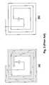
- FIG. 5schematic diagrams of various connections for an embodiment of the present invention comprising a step-tunable inductor having trimming branches are illustrated.
- a spiral inductor represented by the numeral 500has tuning branches A, B and C.
- the self inductance of a segment, or the mutual inductance with adjacent conductorswill vary if two of the branches are cut off. Therefore, the total inductance of the circuit will be changed by trimming the branches A, B and C in the inductor 500 .
- Example (b)has the smallest total inductance value among the examples (b)-(d).
- the trimmingcutting off of trimming branches) causes changes in geometric parameters of the coil of the inductor 500 , such as segment length and spacing between the segments, thereby changing the total inductance.
- FIG. 6illustrates a schematic block diagram of an inductively tuned antenna circuit RFID tag, according to embodiments of the invention.
- the parallel resonant antenna circuit 106comprises a fixed capacitor 110 , a fixed inductor 108 and a step adjustable inductor 608 .
- the capacitor 110may be part of the RFID device 202 .
- the inductance of the step adjustable inductor 608is adjusted to resonate the antenna circuit 106 to a desired frequency. Adjustment of the step adjustable inductor 608 is done by cutting the appropriate trimming branches for a desired change in inductance.
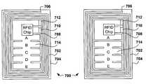
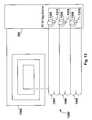
- FIG. 7a schematic plan view of an embodiment of an RFID tag 700 is illustrated.
- the antenna inductor 702 illustratedhas four spiral turns which are etched from conductive material such as metal deposited on a dielectric (insulated) substrate 704 .
- the first spiral turnstarts from point 706 and the fourth spiral turn ends at point 708 .
- Jumper 712connects point 706 to the RFID device 716 and fixed value capacitor 710 .
- Segments A, B, C, D and Eare trimming branches.
- the total geometric parameters (physical dimension) of the inductor 702 , or the inner diameter, of the inductor 702changes by cutting off all but one of the trimming branches.
- Each of the segments A, B, C, D and Erepresent a different inductance value of the inductor 702 .
- the inductance value of the inductor 702can be adjusted by selectively cutting all but one of these segments.
- the inductor 702can be tuned to a desired frequency in combination with a fixed value capacitor 710 on the substrate 704 or integrated into the RFID chip 716 .
- FIG. 8illustrates the trimming branches A-D cut off, and branch E intact.
- the inductor 702is formed by segments starting from point 706 and ends at point 708 through branch E. This results in a maximum inductance value for the inductor 702 .
- FIG. 9illustrates the trimming branches B-E cut off, and branch A intact.
- the inductor 702is formed by segments starting from point 706 and ends at point 708 through branch A. This results in a minimum inductance value for the inductor 702 .
- the inductance value of the inductor 702may thus be adjusted from a minimum to a maximum value by selectively cutting all but one of the trimming branches A-E.
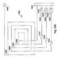
- FIG. 10illustrates a schematic diagram of an embodiment of an inductor having fuse link selection of series connected coil turns of the inductor.
- FIG. 10Aillustrates a schematic plan view of the inductor of FIG. 10 .
- the inductorgenerally represented by the numeral 1000 , comprises a plurality of series connected coil turns.
- the coil 1000comprises a main inductor 1002 , and a plurality of series connected turns 1004 , 1006 and 1008 which may be initially shorted together by fuse links 1014 , 1016 and 1018 , respectively.
- the fuse link 1014shorts together coil turns 1004 , 1006 and 1008 ;
- the fusible link 1016shorts together coil turns 1006 and 1008 ;
- the fuse link 1018shorts together coil turn 1008 .
- the inductance value of the inductor 1000may be increased by causing selected fuse links to open, thereby adding the inductance of one or more of the coil turns 1004 - 1008 to the inductance of the main inductor 1002 .
- the capacitors 1034 , 1036 and 1038are merely direct current blocking capacitors and appear as radio frequency “short circuits” at the operating frequencies of interest.
- Connection nodes 1024 , 1026 , 1028 and 1040are adapted for application of programming currents to the fusible links 1014 , 1016 and 1018 .
- the fuse link 1014is opened by applying sufficient current between nodes 1024 and 1040 to melt or blow open the fuse link 1014 .
- the fuse links 1014 and 1016are opened by applying sufficient current between nodes 1024 and 1040 and nodes 1026 and 1040 to melt or blow open the fuse links 1014 and 1016 , respectively.
- the fuse links 1014 , 1016 and 1018are opened by applying sufficient current between nodes 1024 and 1040 , 1026 and 1040 , and 1028 and 1040 to melt or blow open the fuse links 1014 , 1016 and 1018 , respectively.
- FIG. 11illustrates a schematic diagram of another fuse link controlled embodiment of the invention.
- the antenna inductorgenerally represented by the numeral 1100 has, for example but is not limited to, four spiral turns which may be etched from conductive material such as metal deposited on a dielectric (insulated) substrate (not illustrated).
- Four segments comprising fuse links 1102 , 1104 , 1106 and 1108function as trimming branches as described above.
- the total geometric parameters (physical dimension) of the inductor 1100 , or the inner diameter, of the inductor 1100changes by opening one or more of the fuse link trimming branches (fuse links 1102 , 1104 , 1106 and 1108 ). This allows the inductance value of the inductor 1100 to be selectively adjusted.
- the inductor 1100can be tuned to a desired resonant frequency in combination with the fixed value capacitor 1110 .
- the length of the inner diameter coil turnis made up of segments 1124 and 1126 , and DC blocking capacitor 1130 .
- Each of the fuse links 1102 , 1104 , 1106 and 1108represents a different inductance value of the inductor 1100 .
- Each of the fuse links 1102 , 1104 , 1106 and 1108require a different value of current to open the respective fuse link.
- Capacitor 1130blocks direct current (DC) so that the programming current will flow only through the fuse links 1102 , 1104 , 1106 and 1108 .
- the lowest value current fuse linkis 1102 and the next higher value current is for fuse link 1104 , the next is fuse link 1106 and the highest current value is fuse link 1108 .
- the desired number of fuse linksmay be opened.
- FIG. 12illustrates a schematic diagram of another fuse link controlled embodiment of the invention.
- the antenna inductorgenerally represented by the numeral 1200 has, for example but is not limited to, four spiral turns which may be etched from conductive material such as metal deposited on a dielectric (insulated) substrate (not illustrated).
- Four segmentscomprising fuse links 1202 , 1204 , 1206 and 1208 and resistors 1212 , 1214 , 1216 and 1218 function as trimming branches as described above.
- the total geometric parameters (physical dimension) of the inductor 1200 , or the inner diameter, of the inductor 1200changes by opening one or more of the fuse link trimming branches (fuse links 1202 , 1204 , 1206 and 1208 ).
- the inductance value of the inductor 1200can be selectively adjusted. Whereby the inductor 1200 can be tuned to a desired resonant frequency in combination with the fixed value capacitor 1210 .
- the length of the inner diameter coil turnis made up of segments 1124 and 1126 , and DC blocking capacitor 1230 .
- Each of the fuse links 1202 , 1204 , 1206 and 1208represents a different inductance value of the inductor 1200 .
- the fuse links 1202 , 1204 , 1206 and 1208may all have the same current operating value but the resistors 1212 , 1214 , 1216 and 1218 have difference values which require a different value of voltage to open the respective fuse link. The higher the value of resistor the lower the current flow for a given current.
- resistor 1218By making resistor 1218 a higher resistance value than resistor 1216 , resistor 1216 a higher resistance value than resistor 1214 , and resistor 1214 a higher resistance value than resistor 1212 ; the fuse link 1202 will open at the lowest voltage value applied between nodes 1220 and 1222 . Fuse link 1204 will open at the next voltage value increase, fuse link 1206 will open at the next higher voltage value increase, and fuse link 1208 will open at the highest voltage value applied between nodes 1220 and 1222 .
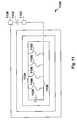
- FIG. 13illustrates a schematic diagram of an embodiment of inductive tuning being controlled by circuits of the semiconductor RFID tag device.
- An inductorgenerally represented by the numeral 1300 , comprises a plurality of series connected coil turns.
- the coil 1300comprises a main inductor 1302 , and a plurality of series connected turns 1304 , 1306 and 1308 which may be initially shorted together by transistor switches 1324 , 1326 and 1328 , respectively.
- the transistor switches 1324 , 1326 and 1328may be controlled by programmable fuse links 1314 , 1316 and 1318 , respectively.
- the transistor switch 1324shorts together coil turns 1304 , 1306 and 1308 ; the transistor switch 1326 shorts together coil turns 1306 and 1308 ; and the transistor switch 1328 shorts together coil turn 1308 .
- the inductance value of the inductor 1300may be increased by causing selected fuse links to open, thereby adding the inductance of one or more of the coil turns 1304 - 1308 to the inductance of the main inductor 1302 .
- FIG. 14illustrates a schematic diagram of an automatic tuning embodiment of the invention.
- An inductorgenerally represented by the numeral 1400 , comprises a plurality of series connected coil turns.
- the coil 1400comprises a main inductor 1402 , and a plurality of series connected turns 1404 , 1406 and 1408 which may be initially shorted together by transistor switches 1424 , 1426 and 1428 , respectively.
- the transistor switches 1424 , 1426 and 1428may be controlled by a frequency selection circuit 1412 .
- the transistor switch 1424shorts together coil turns 1404 , 1406 and 1408 ; the transistor switch 1426 shorts together coil turns 1406 and 1408 ; and the transistor switch 1428 shorts together coil turn 1408 .
- the inductance value of the inductor 1400may be thereby adjusted so as to tune the parallel resonant circuit of the inductor 1400 and capacitor (not illustrated) to an optimum frequency determined by the frequency determining and optimization circuit 1412 .
- the frequency selection circuit 1412preferably may be part of the RFID tag device 1410 .
- the RFID tag devicemay comprise a microcontroller functioning as the frequency selection circuit 1412 .
Landscapes
- Engineering & Computer Science (AREA)
- Physics & Mathematics (AREA)
- General Physics & Mathematics (AREA)
- Theoretical Computer Science (AREA)
- Computer Hardware Design (AREA)
- Microelectronics & Electronic Packaging (AREA)
- Computer Networks & Wireless Communication (AREA)
- Semiconductor Integrated Circuits (AREA)
Abstract
Description


Claims (33)
Priority Applications (3)
| Application Number | Priority Date | Filing Date | Title |
|---|---|---|---|
| US09/728,190US6480110B2 (en) | 2000-12-01 | 2000-12-01 | Inductively tunable antenna for a radio frequency identification tag |
| AU2002225905AAU2002225905A1 (en) | 2000-12-01 | 2001-12-03 | Inductively tunable antenna for a radio frequency identification tag |
| PCT/US2001/046388WO2002045011A1 (en) | 2000-12-01 | 2001-12-03 | Inductively tunable antenna for a radio frequency identification tag |
Applications Claiming Priority (1)
| Application Number | Priority Date | Filing Date | Title |
|---|---|---|---|
| US09/728,190US6480110B2 (en) | 2000-12-01 | 2000-12-01 | Inductively tunable antenna for a radio frequency identification tag |
Publications (2)
| Publication Number | Publication Date |
|---|---|
| US20020097153A1 US20020097153A1 (en) | 2002-07-25 |
| US6480110B2true US6480110B2 (en) | 2002-11-12 |
Family
ID=24925780
Family Applications (1)
| Application Number | Title | Priority Date | Filing Date |
|---|---|---|---|
| US09/728,190Expired - LifetimeUS6480110B2 (en) | 2000-12-01 | 2000-12-01 | Inductively tunable antenna for a radio frequency identification tag |
Country Status (3)
| Country | Link |
|---|---|
| US (1) | US6480110B2 (en) |
| AU (1) | AU2002225905A1 (en) |
| WO (1) | WO2002045011A1 (en) |
Cited By (88)
| Publication number | Priority date | Publication date | Assignee | Title |
|---|---|---|---|---|
| US20020167407A1 (en)* | 1999-12-07 | 2002-11-14 | Manfred Fries | Product label, method of producing product labels and method for identifying products in a contactless and forgery-proof manner |
| US20020186175A1 (en)* | 1999-12-16 | 2002-12-12 | Lassina Sanogo | Radio frequency antenna for an object interrogation device comprising a radio frequency antenna associated with an electronic circuit |
| US20030029540A1 (en)* | 2000-01-17 | 2003-02-13 | Rafsec Oy | Method for the manufacture of a smart label inlet web, and a smart label inlet web |
| US20030052077A1 (en)* | 2000-03-31 | 2003-03-20 | Rafsec Oy | Method for forming a product sensor, and a product sensor |
| US20030078807A1 (en)* | 2001-10-22 | 2003-04-24 | Siemens Medical Solutions Health Services Corporation | System for maintaining organization related information for use in supporting organization operation |
| US20030080918A1 (en)* | 2001-10-29 | 2003-05-01 | Forster Ian James | Wave antenna wireless communication device and method |
| US20030127525A1 (en)* | 2000-06-06 | 2003-07-10 | Rafsec Oy | Smart card web and a method for its manufacture |
| US20030132893A1 (en)* | 2001-10-29 | 2003-07-17 | Forster Ian J. | Wave antenna wireless communication device and method |
| US6597318B1 (en)* | 2002-06-27 | 2003-07-22 | Harris Corporation | Loop antenna and feed coupler for reduced interaction with tuning adjustments |
| US20030218072A1 (en)* | 2000-11-01 | 2003-11-27 | Rafsac Oy | Method for the manufacture of a smart label, and a smart label |
| US20040027241A1 (en)* | 2002-08-08 | 2004-02-12 | Forster Ian J. | Vehicle tag reader |
| US20040032377A1 (en)* | 2001-10-29 | 2004-02-19 | Forster Ian James | Wave antenna wireless communication device and method |
| US20040036572A1 (en)* | 2002-04-24 | 2004-02-26 | Forster Ian J. | Wireless communication device having conductive elements antenna |
| US20040046665A1 (en)* | 2002-09-06 | 2004-03-11 | Douglas Narlow | Deactivatable radio frequency security label |
| US20040056781A1 (en)* | 2002-09-19 | 2004-03-25 | Rix Scott M. | Computer input device with individually positionable and programmable input members |
| WO2004053721A1 (en)* | 2002-12-10 | 2004-06-24 | Shalom Wertsberger | Deactivation of radio frequency identification tags |
| US20040169586A1 (en)* | 2001-05-31 | 2004-09-02 | Rafsac Oy | Smart label and a smart label web |
| US20040245858A1 (en)* | 2002-03-13 | 2004-12-09 | Devilbiss Alan D. | Rectifier utilizing a grounded antenna |
| US20040257229A1 (en)* | 2003-03-26 | 2004-12-23 | Proximities | Non-reusable identification device |
| US20040263319A1 (en)* | 2003-06-30 | 2004-12-30 | Nokia Corporation | System and method for supporting multiple reader-tag configurations using multi-mode radio frequency tag |
| US6839035B1 (en)* | 2003-10-07 | 2005-01-04 | A.C.C. Systems | Magnetically coupled antenna range extender |
| US20050012616A1 (en)* | 2003-07-07 | 2005-01-20 | Forster Ian J. | RFID device with changeable characteristics |
| US20050025943A1 (en)* | 2001-07-04 | 2005-02-03 | Anu Krappe | Injection moulded product and a method for its manufacture |
| US20050030201A1 (en)* | 2003-04-21 | 2005-02-10 | Raj Bridgelall | Method for optimizing the design and implementation of RFID tags |
| US20050087607A1 (en)* | 2001-12-21 | 2005-04-28 | Samuli Stromberg | Smart label web and a method for its manufacture |
| US20050093761A1 (en)* | 2002-08-14 | 2005-05-05 | King Patrick F. | RFID tire belt antenna system and method |
| US20050195082A1 (en)* | 2004-03-08 | 2005-09-08 | Nuvo Holdings, Llc | RF Communications Apparatus and Manufacturing Method Therefor |
| US20050212707A1 (en)* | 2004-03-23 | 2005-09-29 | Egbert William C | Radio frequency identification tags with compensating elements |
| US20050237198A1 (en)* | 2004-04-08 | 2005-10-27 | Waldner Michele A | Variable frequency radio frequency indentification (RFID) tags |
| US20060033624A1 (en)* | 2004-08-13 | 2006-02-16 | Copeland Richard L | Tunable antenna |
| US20060044192A1 (en)* | 2003-12-23 | 2006-03-02 | 3M Innovative Properties Company | Ultra high frequency radio frequency identification tag |
| US20060094425A1 (en)* | 2004-10-28 | 2006-05-04 | Mickle Marlin H | Recharging apparatus |
| US20060152364A1 (en)* | 2004-12-30 | 2006-07-13 | Walton Charles A | RFID with field changeable identification |
| US20060195705A1 (en)* | 2005-02-28 | 2006-08-31 | Cypak Ab | Tamper Evident Seal System and Method |
| US20060212241A1 (en)* | 2005-03-04 | 2006-09-21 | Chiu Lihu M | RFID tag imager |
| US20060238308A1 (en)* | 2005-04-21 | 2006-10-26 | University Of Pittsburgh-Of The Commonwealth System Of Higher Education | Methods and apparatus for reducing power consumption of an active transponder |
| US20070029481A1 (en)* | 2003-08-01 | 2007-02-08 | Robert Morrison | Specimen tip and tip holder assembly |
| US20070126589A1 (en)* | 2004-12-20 | 2007-06-07 | Linda Jacober | RFID Tag Label |
| US20070158441A1 (en)* | 2006-01-11 | 2007-07-12 | Infineon Technologies Ag | Identification data carrier, read device, identification system and procedure for manufacturing an identification data carrier |
| US7244332B2 (en) | 2000-12-11 | 2007-07-17 | Rafsec Oy | Smart label web and a method for its manufacture |
| US20070176752A1 (en)* | 2005-04-21 | 2007-08-02 | University Of Pittsburgh - Of The Commonwealth System Of Higher Education | Methods and apparatus for reducing power consumption of an active transponder |
| US20070200705A1 (en)* | 2006-02-24 | 2007-08-30 | Fujitsu Limited | RFID tag |
| US20070205873A1 (en)* | 2006-02-23 | 2007-09-06 | Mickle Marlin H | Methods and apparatus for switching a transponder to an active state, and asset management systems employing same |
| US20070222602A1 (en)* | 2006-03-17 | 2007-09-27 | Macronix International Co., Ltd. | Systems and methods for enhancing the magnetic coupling in a wireless communication system |
| US20070246716A1 (en)* | 2006-04-21 | 2007-10-25 | Philips Lumileds Lighting Company, Llc | Semiconductor light emitting device with integrated electronic components |
| US20070257268A1 (en)* | 2004-09-13 | 2007-11-08 | Yukio Shakuda | Semiconductor Light Emitting Device |
| US20070296548A1 (en)* | 2006-06-27 | 2007-12-27 | Hall Stewart E | Resonant circuit tuning system using magnetic field coupled reactive elements |
| US20080055044A1 (en)* | 2006-08-31 | 2008-03-06 | 3M Innovative Properties Company | Flame resistant rfid tag and method of making the same |
| US20080100446A1 (en)* | 2006-10-27 | 2008-05-01 | Sony Corporation | Radio frequency identification system |
| US7397378B1 (en)* | 2005-02-21 | 2008-07-08 | Leason Holdings Company, L.L.C. | Selectively responsive tag suitable for RFID systems and the like |
| US7429926B1 (en)* | 2005-07-20 | 2008-09-30 | Xilinx, Inc. | Radio frequency identification (RFID) and programmable logic device (PLD) integration and applications |
| US20080284605A1 (en)* | 2005-03-07 | 2008-11-20 | Gary Mark Shafer | Automated Tuning Method for Rfid Labels |
| US20090027162A1 (en)* | 2007-07-23 | 2009-01-29 | Forster Ian J | Controllable rfid device, and method |
| US20090051539A1 (en)* | 2007-08-22 | 2009-02-26 | Sensormatic Electronics Corporation | Rfid tag having antenna with co-planar radiation pattern |
| US20090085750A1 (en)* | 2007-09-27 | 2009-04-02 | 3M Innovative Properties Company | Extended RFID tag |
| US20090085746A1 (en)* | 2007-09-27 | 2009-04-02 | 3M Innovative Properties Company | Signal line structure for a radio-frequency identification system |
| US20090096696A1 (en)* | 2007-10-11 | 2009-04-16 | Joyce Jr Terrence H | Rfid tag with a modified dipole antenna |
| US20090109003A1 (en)* | 2007-09-24 | 2009-04-30 | Cooper Tire & Rubber Cumpany | Automatic antenna tuner system for RFID |
| US20090128436A1 (en)* | 2005-04-14 | 2009-05-21 | Agency For Science, Technology And Research | On-chip inductor with trimmable inductance, a method for making the same and a method for adjusting the impedance of the inductance |
| US20090153275A1 (en)* | 2007-12-12 | 2009-06-18 | Electronics And Telecommunications Research Institute | Tunable magnetic field amplifying device |
| US7562445B2 (en) | 2005-07-18 | 2009-07-21 | Bartronics America, Inc. | Method of manufacture of an identification wristband construction |
| US20090189742A1 (en)* | 2008-01-24 | 2009-07-30 | Kabushiki Kaisha Toshiba | Radio communication device and radio communication system |
| US20090207026A1 (en)* | 2008-02-14 | 2009-08-20 | Banerjee Swagata R | Radio frequency identification (rfid) tag including a three-dimensional loop antenna |
| US20090224055A1 (en)* | 2008-03-07 | 2009-09-10 | Infineon Technologies Ag | Integrated ciruit device including tunable substrate capacitors |
| US20090243397A1 (en)* | 2008-03-05 | 2009-10-01 | Nigel Power, Llc | Packaging and Details of a Wireless Power device |
| US20090243805A1 (en)* | 2008-04-01 | 2009-10-01 | Ls Industrial Systems Co., Ltd. | Rfid tag and rfid system using the same |
| US20100001839A1 (en)* | 2006-10-25 | 2010-01-07 | Jirou Uchiyama | Communication apparatus and portable communication terminal using the same |
| US20100022063A1 (en)* | 2008-07-28 | 2010-01-28 | Mete Erturk | Method of forming on-chip passive element |
| US20100019346A1 (en)* | 2008-07-28 | 2010-01-28 | Mete Erturk | Ic having flip chip passive element and design structure |
| US20100073188A1 (en)* | 2008-09-25 | 2010-03-25 | University Of Pittsburgh- Of The Commonwealth System Of Higher Education | System and Method for Real Time Asset Location and Tracking |
| US20100130096A1 (en)* | 2008-11-21 | 2010-05-27 | Access Business Group International Llc | Inductive toy vehicle |
| US20100181961A1 (en)* | 2009-01-22 | 2010-07-22 | Qualcomm Incorporated | Adaptive power control for wireless charging |
| US20100321164A1 (en)* | 2009-06-19 | 2010-12-23 | Stmicroelectronics (Rousset) Sas | Inductive evaluation of the coupling factor of an electromagnetic transponder |
| US20110031319A1 (en)* | 2009-08-05 | 2011-02-10 | Perfect Plastic Printing Corporation | RF Proximity Financial Transaction Card Having Metallic Foil Layer(s) |
| US20110163161A1 (en)* | 2008-08-25 | 2011-07-07 | Nxp B.V. | Reconfigurable radio-frequency front-end |
| US20110205028A1 (en)* | 2010-02-25 | 2011-08-25 | Stmicroelectronics S.R.L. | Electronic communications device with antenna and electromagnetic shield |
| US20130093252A1 (en)* | 2011-04-08 | 2013-04-18 | Access Business Group International Llc | Counter wound inductive power supply |
| US20130293354A1 (en)* | 2012-05-01 | 2013-11-07 | Jeevan Kumar Vemagiri | Discontinuous loop antennas suitable for radio-frequency identification (rfid) tags, and related components, systems, and methods |
| US20140266542A1 (en)* | 2013-03-15 | 2014-09-18 | Taiwan Semiconductor Manufacturing Company, Ltd. | Programmable Inductor |
| US9450456B2 (en) | 2008-04-21 | 2016-09-20 | Qualcomm Incorporated | System and method for efficient wireless power transfer to devices located on and outside a charging base |
| US20170354867A1 (en)* | 2016-06-10 | 2017-12-14 | Nintendo Co., Ltd. | Game controller |
| US10335675B2 (en) | 2016-06-10 | 2019-07-02 | Nintendo Co., Ltd. | Game controller |
| US10388462B2 (en) | 2015-07-15 | 2019-08-20 | Michael J. Dueweke | Tunable reactance devices, and methods of making and using the same |
| US10441878B2 (en)* | 2016-06-10 | 2019-10-15 | Nintendo Co., Ltd. | Game controller |
| US10491159B2 (en) | 2016-09-07 | 2019-11-26 | Michael J. Dueweke | Self-tuning microelectromechanical impedance matching circuits and methods of fabrication |
| US10835811B2 (en) | 2016-06-10 | 2020-11-17 | Nintendo Co., Ltd. | Game controller |
| US10864436B2 (en) | 2016-06-10 | 2020-12-15 | Nintendo Co., Ltd. | Game controller |
| US11176338B1 (en)* | 2019-11-01 | 2021-11-16 | Bae Systems Information And Electronic Systems Integration Inc. | On-chip RF interrogation for heterogeneous RFIDS |
Families Citing this family (31)
| Publication number | Priority date | Publication date | Assignee | Title |
|---|---|---|---|---|
| US7037298B2 (en)* | 2001-12-20 | 2006-05-02 | The Procter & Gamble Company | Disposable absorbent article having a raised circumferential bank |
| SG112842A1 (en)* | 2002-06-28 | 2005-07-28 | Tunity Pte Ltd | Passive range extender/booster for rfid tag/reader |
| US20040201539A1 (en)* | 2003-04-09 | 2004-10-14 | Yewen Robert G. | Radio frequency identification system and antenna system |
| US7398926B1 (en)* | 2003-10-06 | 2008-07-15 | Applied Wireless Identifications Group, Inc. | Apparatus and method for programming an RFID transponder using a constrained field |
| US7202768B1 (en) | 2003-12-10 | 2007-04-10 | Dsp Group Inc. | Tunable inductor |
| US20070273476A1 (en)* | 2004-03-26 | 2007-11-29 | Semiconductor Energy Laboratory Co., Ltd. | Thin Semiconductor Device And Operation Method Of Thin Semiconductor Device |
| US8134445B2 (en)* | 2004-04-20 | 2012-03-13 | Cooper Technologies Company | RFID open fuse indicator, system, and method |
| US7804411B2 (en)* | 2004-11-15 | 2010-09-28 | Sensormatic Electronics, LLC | Combination EAS and RFID label or tag using a hybrid RFID antenna |
| BRPI0518913B1 (en)* | 2004-11-15 | 2019-01-02 | Sensormatic Electronics Corp | security tag and method of operating a combination of an eas and an rfid |
| US20070096891A1 (en)* | 2005-10-17 | 2007-05-03 | Sheriff Michael L | RFID buckle closure and presence sensor system for safety childseat |
| US8026818B2 (en)* | 2006-12-20 | 2011-09-27 | Checkpoint Systems, Inc. | EAS and UHF combination tag |
| US9294157B2 (en)* | 2007-08-20 | 2016-03-22 | Gui-Yang Lu | Radio-frequency identification system |
| IL188089A (en)* | 2007-12-12 | 2013-02-28 | Nds Ltd | Bit generator |
| FI20086035A0 (en)* | 2008-11-03 | 2008-11-03 | Pulse Finland Oy | Tunable antenna and antenna tuning system |
| US20100148965A1 (en)* | 2008-12-16 | 2010-06-17 | Sensormatic Electronics Corporation | Method and system for item level uhf rfid tag with low frequency power assist |
| JP5583042B2 (en)* | 2011-02-04 | 2014-09-03 | 株式会社デンソー | Electronic control unit |
| US8746576B2 (en) | 2011-08-25 | 2014-06-10 | Elwha Llc | Systems, devices, admixtures, and methods including transponders for indication of food attributes |
| US20130049932A1 (en)* | 2011-08-25 | 2013-02-28 | Elwha LLC, a limited liability company of the State of Delaware | Systems, devices, methods, and admixtures of transponders and food products for indication of food attributes |
| DE102012015406A1 (en)* | 2012-08-01 | 2014-02-06 | Gantner Electronic Gmbh | Method and device for optimizing the RFID field of an access control device |
| DE102012113043A1 (en)* | 2012-12-21 | 2014-06-26 | Endress + Hauser Conducta Gesellschaft für Mess- und Regeltechnik mbH + Co. KG | System for contact-less energy and data transfer between primary winding and secondary winding, has resonant circuit whose resonant frequency is changed by directly switching-on and/or switching-off of individual branches by switching unit |
| US20150054704A1 (en)* | 2013-08-23 | 2015-02-26 | Samsung Sdi Co., Ltd. | Antenna module for terminal device and method for manufacturing the same |
| WO2017055917A1 (en)* | 2015-10-01 | 2017-04-06 | Star Systems International, Ltd. | Switchable radio-frequency identification tag device |
| US10055619B2 (en) | 2016-06-17 | 2018-08-21 | Intermec, Inc. | Systems and methods for compensation of interference in radiofrequency identification (RFID) devices |
| ES2974324T3 (en)* | 2017-06-22 | 2024-06-26 | Checkpoint Systems Inc | Detectable folded coil |
| US11544518B2 (en)* | 2017-06-22 | 2023-01-03 | Checkpoint Systems, Inc. | Deactivatable metal tag |
| CN107766906A (en)* | 2017-11-20 | 2018-03-06 | 福建师范大学福清分校 | Steel corrosion detecting system and detection method based on high frequency passive RFID label tag |
| CN108448227A (en)* | 2018-03-28 | 2018-08-24 | 武汉纺织大学 | A reader antenna suitable for dense containers |
| GB2580093B (en)* | 2018-12-21 | 2021-08-25 | Pragmatic Printing Ltd | An RFID system with improved signal transmission characteristics |
| US12223814B2 (en) | 2019-09-16 | 2025-02-11 | Sensormatic Electronics, LLC | Security tag for textiles using conductive thread |
| US10783424B1 (en)* | 2019-09-18 | 2020-09-22 | Sensormatic Electronics, LLC | Systems and methods for providing tags adapted to be incorporated with or in items |
| US11443160B2 (en) | 2019-09-18 | 2022-09-13 | Sensormatic Electronics, LLC | Systems and methods for laser tuning and attaching RFID tags to products |
Citations (15)
| Publication number | Priority date | Publication date | Assignee | Title |
|---|---|---|---|---|
| US4021705A (en)* | 1975-03-24 | 1977-05-03 | Lichtblau G J | Resonant tag circuits having one or more fusible links |
| US4857893A (en) | 1986-07-18 | 1989-08-15 | Bi Inc. | Single chip transponder device |
| US5276431A (en) | 1992-04-29 | 1994-01-04 | Checkpoint Systems, Inc. | Security tag for use with article having inherent capacitance |
| US5337063A (en)* | 1991-04-22 | 1994-08-09 | Mitsubishi Denki Kabushiki Kaisha | Antenna circuit for non-contact IC card and method of manufacturing the same |
| US5574470A (en) | 1994-09-30 | 1996-11-12 | Palomar Technologies Corporation | Radio frequency identification transponder apparatus and method |
| US5682143A (en) | 1994-09-09 | 1997-10-28 | International Business Machines Corporation | Radio frequency identification tag |
| US5734327A (en)* | 1992-11-27 | 1998-03-31 | Dutch A & A Trading B.V. | Detection tag |
| US5781110A (en)* | 1996-05-01 | 1998-07-14 | James River Paper Company, Inc. | Electronic article surveillance tag product and method of manufacturing same |
| US5821525A (en)* | 1994-08-03 | 1998-10-13 | Mitsubishi Denki Kabushiki Kaisha | Reader/writer for use with non-contact IC card and reader/writer system |
| US5926094A (en) | 1994-11-28 | 1999-07-20 | Mamou; Patrick | Antitheft label and process for its deactivation, in particular for clothing articles |
| US6028564A (en)* | 1997-01-29 | 2000-02-22 | Intermec Ip Corp. | Wire antenna with optimized impedance for connecting to a circuit |
| US6091332A (en) | 1998-06-09 | 2000-07-18 | Motorola, Inc. | Radio frequency identification tag having printed circuit interconnections |
| US6100804A (en) | 1998-10-29 | 2000-08-08 | Intecmec Ip Corp. | Radio frequency identification system |
| US6198381B1 (en) | 1997-09-26 | 2001-03-06 | Data Investments Limited | Delayed reset mode model for electronic identification systems |
| US6210995B1 (en)* | 1999-09-09 | 2001-04-03 | International Business Machines Corporation | Method for manufacturing fusible links in a semiconductor device |
Family Cites Families (1)
| Publication number | Priority date | Publication date | Assignee | Title |
|---|---|---|---|---|
| JPS61256611A (en)* | 1985-05-08 | 1986-11-14 | Fujitsu Ltd | Manufacturing method of variable chip inductor |
- 2000
- 2000-12-01USUS09/728,190patent/US6480110B2/ennot_activeExpired - Lifetime
- 2001
- 2001-12-03WOPCT/US2001/046388patent/WO2002045011A1/ennot_activeApplication Discontinuation
- 2001-12-03AUAU2002225905Apatent/AU2002225905A1/ennot_activeAbandoned
Patent Citations (15)
| Publication number | Priority date | Publication date | Assignee | Title |
|---|---|---|---|---|
| US4021705A (en)* | 1975-03-24 | 1977-05-03 | Lichtblau G J | Resonant tag circuits having one or more fusible links |
| US4857893A (en) | 1986-07-18 | 1989-08-15 | Bi Inc. | Single chip transponder device |
| US5337063A (en)* | 1991-04-22 | 1994-08-09 | Mitsubishi Denki Kabushiki Kaisha | Antenna circuit for non-contact IC card and method of manufacturing the same |
| US5276431A (en) | 1992-04-29 | 1994-01-04 | Checkpoint Systems, Inc. | Security tag for use with article having inherent capacitance |
| US5734327A (en)* | 1992-11-27 | 1998-03-31 | Dutch A & A Trading B.V. | Detection tag |
| US5821525A (en)* | 1994-08-03 | 1998-10-13 | Mitsubishi Denki Kabushiki Kaisha | Reader/writer for use with non-contact IC card and reader/writer system |
| US5682143A (en) | 1994-09-09 | 1997-10-28 | International Business Machines Corporation | Radio frequency identification tag |
| US5574470A (en) | 1994-09-30 | 1996-11-12 | Palomar Technologies Corporation | Radio frequency identification transponder apparatus and method |
| US5926094A (en) | 1994-11-28 | 1999-07-20 | Mamou; Patrick | Antitheft label and process for its deactivation, in particular for clothing articles |
| US5781110A (en)* | 1996-05-01 | 1998-07-14 | James River Paper Company, Inc. | Electronic article surveillance tag product and method of manufacturing same |
| US6028564A (en)* | 1997-01-29 | 2000-02-22 | Intermec Ip Corp. | Wire antenna with optimized impedance for connecting to a circuit |
| US6198381B1 (en) | 1997-09-26 | 2001-03-06 | Data Investments Limited | Delayed reset mode model for electronic identification systems |
| US6091332A (en) | 1998-06-09 | 2000-07-18 | Motorola, Inc. | Radio frequency identification tag having printed circuit interconnections |
| US6100804A (en) | 1998-10-29 | 2000-08-08 | Intecmec Ip Corp. | Radio frequency identification system |
| US6210995B1 (en)* | 1999-09-09 | 2001-04-03 | International Business Machines Corporation | Method for manufacturing fusible links in a semiconductor device |
Cited By (221)
| Publication number | Priority date | Publication date | Assignee | Title |
|---|---|---|---|---|
| US20020167407A1 (en)* | 1999-12-07 | 2002-11-14 | Manfred Fries | Product label, method of producing product labels and method for identifying products in a contactless and forgery-proof manner |
| US7012531B2 (en)* | 1999-12-07 | 2006-03-14 | Infineon Technologies Ag | Product label, method of producing product labels and method for identifying products in a contactless and forgery-proof manner |
| US20020186175A1 (en)* | 1999-12-16 | 2002-12-12 | Lassina Sanogo | Radio frequency antenna for an object interrogation device comprising a radio frequency antenna associated with an electronic circuit |
| US6894660B2 (en)* | 1999-12-16 | 2005-05-17 | Tagsys Sa | Radio frequency antenna for an object interrogation device comprising a radio frequency antenna associated with an electronic circuit |
| US20030029540A1 (en)* | 2000-01-17 | 2003-02-13 | Rafsec Oy | Method for the manufacture of a smart label inlet web, and a smart label inlet web |
| US20030052077A1 (en)* | 2000-03-31 | 2003-03-20 | Rafsec Oy | Method for forming a product sensor, and a product sensor |
| US6951621B2 (en) | 2000-03-31 | 2005-10-04 | Rafsec Oy | Method for forming a product sensor, and a product sensor |
| US20030127525A1 (en)* | 2000-06-06 | 2003-07-10 | Rafsec Oy | Smart card web and a method for its manufacture |
| US20030218072A1 (en)* | 2000-11-01 | 2003-11-27 | Rafsac Oy | Method for the manufacture of a smart label, and a smart label |
| US7244332B2 (en) | 2000-12-11 | 2007-07-17 | Rafsec Oy | Smart label web and a method for its manufacture |
| US7066393B2 (en) | 2001-05-31 | 2006-06-27 | Rafsec Oy | Smart label and a smart label web |
| US20040169586A1 (en)* | 2001-05-31 | 2004-09-02 | Rafsac Oy | Smart label and a smart label web |
| US7199456B2 (en) | 2001-07-04 | 2007-04-03 | Rafsec Oy | Injection moulded product and a method for its manufacture |
| US20050025943A1 (en)* | 2001-07-04 | 2005-02-03 | Anu Krappe | Injection moulded product and a method for its manufacture |
| US20030078807A1 (en)* | 2001-10-22 | 2003-04-24 | Siemens Medical Solutions Health Services Corporation | System for maintaining organization related information for use in supporting organization operation |
| US7916095B2 (en) | 2001-10-29 | 2011-03-29 | Mineral Lassen Llc | Wave antenna wireless communication device and method |
| US6895655B2 (en) | 2001-10-29 | 2005-05-24 | Marconi Intellectual Property (Us) Inc. | Wave antenna wireless communication device and method |
| US20060279425A1 (en)* | 2001-10-29 | 2006-12-14 | Mineral Lassen Llc | Wave antenna wireless communication device and method |
| US20070057861A1 (en)* | 2001-10-29 | 2007-03-15 | Forster Ian J | Wave antenna wireless communication device and method |
| US7190319B2 (en) | 2001-10-29 | 2007-03-13 | Forster Ian J | Wave antenna wireless communication device and method |
| US7345643B2 (en) | 2001-10-29 | 2008-03-18 | Mineral Lassen Llc | Wave antenna wireless communication device and method |
| US20040032377A1 (en)* | 2001-10-29 | 2004-02-19 | Forster Ian James | Wave antenna wireless communication device and method |
| US7439928B2 (en) | 2001-10-29 | 2008-10-21 | Mineral Lassen Llc | Wave antenna wireless communication device and method |
| US20030132893A1 (en)* | 2001-10-29 | 2003-07-17 | Forster Ian J. | Wave antenna wireless communication device and method |
| US20030117334A1 (en)* | 2001-10-29 | 2003-06-26 | Forster Ian James | Wave antenna wireless communication device and method |
| US7375699B2 (en) | 2001-10-29 | 2008-05-20 | Mineral Lassen Llc | Wave antenna wireless communication device and method |
| US7093345B2 (en) | 2001-10-29 | 2006-08-22 | Ian James Forster | Wave antenna wireless communication device and method |
| US6630910B2 (en)* | 2001-10-29 | 2003-10-07 | Marconi Communications Inc. | Wave antenna wireless communication device and method |
| US7420520B2 (en) | 2001-10-29 | 2008-09-02 | Mineral Lassen Llc | Wave antenna wireless communication device and method |
| US6853347B2 (en) | 2001-10-29 | 2005-02-08 | Marconi Intellectual Property (Us) Inc. | Wave antenna wireless communication device and method |
| US20100231360A1 (en)* | 2001-10-29 | 2010-09-16 | Ian James Forster | Wave antenna wireless communication device and method |
| US7746285B2 (en) | 2001-10-29 | 2010-06-29 | Ian James Forster | Wave antenna wireless communication device and method |
| US20030080919A1 (en)* | 2001-10-29 | 2003-05-01 | Forster Ian James | Wave antenna wireless communication device and method |
| US20030080918A1 (en)* | 2001-10-29 | 2003-05-01 | Forster Ian James | Wave antenna wireless communication device and method |
| US20040041739A1 (en)* | 2001-10-29 | 2004-03-04 | Forster Ian James | Wave antenna wireless communication device and method |
| US6903704B2 (en) | 2001-10-29 | 2005-06-07 | Mineral Lassen Llc | Wave antenna wireless communication device and method |
| US7373713B2 (en) | 2001-10-29 | 2008-05-20 | Mineral Lassen Llc | Wave antenna wireless communication device and method |
| US20060050001A1 (en)* | 2001-10-29 | 2006-03-09 | Mineral Lassen Llc | Wave antenna wireless communication device and method |
| US7394438B2 (en) | 2001-10-29 | 2008-07-01 | Mineral Lassen Llc | Wave antenna wireless communication device and method |
| US20050193549A1 (en)* | 2001-10-29 | 2005-09-08 | Forster Ian J. | Wave antenna wireless communication device and method |
| US20050087607A1 (en)* | 2001-12-21 | 2005-04-28 | Samuli Stromberg | Smart label web and a method for its manufacture |
| US7152803B2 (en) | 2001-12-21 | 2006-12-26 | Upm Rafsec Oy | Smart label web and a method for its manufacture |
| US20040245858A1 (en)* | 2002-03-13 | 2004-12-09 | Devilbiss Alan D. | Rectifier utilizing a grounded antenna |
| US20040036572A1 (en)* | 2002-04-24 | 2004-02-26 | Forster Ian J. | Wireless communication device having conductive elements antenna |
| US7969377B2 (en) | 2002-04-24 | 2011-06-28 | Mineral Lassen Llc | Wireless communication device having conductive elements antenna |
| US20110063177A1 (en)* | 2002-04-24 | 2011-03-17 | Forster Ian J | Wireless communication device having conductive elements antenna |
| US20060290579A1 (en)* | 2002-04-24 | 2006-12-28 | Mineral Lassen Llc | Wireless communication device having conductive elements antenna |
| US20080024384A1 (en)* | 2002-04-24 | 2008-01-31 | Mineral Lassen Llc | Wireless communication device having conductive elements antenna |
| US7327326B2 (en) | 2002-04-24 | 2008-02-05 | Mineral Lassen Llc | Wireless communication device having conductive elements antenna |
| US20090256768A1 (en)* | 2002-04-24 | 2009-10-15 | Mineral Lassen Llc | Wireless communication device having conductive elements antenna |
| US7557767B2 (en) | 2002-04-24 | 2009-07-07 | Forster Ian J | Wireless communication device having conductive elements antenna |
| US7239287B2 (en) | 2002-04-24 | 2007-07-03 | Mineral Lassen Llc | Wireless communication device having conductive elements antenna |
| US7843393B2 (en) | 2002-04-24 | 2010-11-30 | Forster Ian J | Wireless communication device having conductive elements antenna |
| US6597318B1 (en)* | 2002-06-27 | 2003-07-22 | Harris Corporation | Loop antenna and feed coupler for reduced interaction with tuning adjustments |
| US20040027241A1 (en)* | 2002-08-08 | 2004-02-12 | Forster Ian J. | Vehicle tag reader |
| US7586403B2 (en) | 2002-08-08 | 2009-09-08 | Ian J Forster | Vehicle tag reader |
| US20060170540A1 (en)* | 2002-08-08 | 2006-08-03 | Mineral Lassen Llc | Vehicle tag reader |
| US20060192662A1 (en)* | 2002-08-08 | 2006-08-31 | Mineral Lassen Llc | Vehicle tag reader |
| US7518494B2 (en) | 2002-08-08 | 2009-04-14 | Ian J Forster | Vehicle tag reader |
| US7015802B2 (en) | 2002-08-08 | 2006-03-21 | Forster Ian J | Vehicle tag reader |
| US20070013500A1 (en)* | 2002-08-08 | 2007-01-18 | Mineral Lassen Llc | Vehicle tag reader |
| US7479873B2 (en) | 2002-08-08 | 2009-01-20 | Mineral Lassen Llc | Vehicle tag reader |
| US7050017B2 (en) | 2002-08-14 | 2006-05-23 | King Patrick F | RFID tire belt antenna system and method |
| US20050093761A1 (en)* | 2002-08-14 | 2005-05-05 | King Patrick F. | RFID tire belt antenna system and method |
| US20040046665A1 (en)* | 2002-09-06 | 2004-03-11 | Douglas Narlow | Deactivatable radio frequency security label |
| US6919806B2 (en)* | 2002-09-06 | 2005-07-19 | Sensormatic Electronics Corporation | Deactivatable radio frequency security label |
| WO2004023416A3 (en)* | 2002-09-06 | 2004-11-25 | Sensormatic Electronics Corp | Deactivatable radio frequency security label |
| WO2004027558A3 (en)* | 2002-09-19 | 2004-06-10 | Ergodex | Computer input device with individually positionable and programmable input members |
| US20040056781A1 (en)* | 2002-09-19 | 2004-03-25 | Rix Scott M. | Computer input device with individually positionable and programmable input members |
| WO2004053721A1 (en)* | 2002-12-10 | 2004-06-24 | Shalom Wertsberger | Deactivation of radio frequency identification tags |
| US20050146435A1 (en)* | 2003-03-26 | 2005-07-07 | Proximities, Inc. | Non-reusable identification device |
| US20060187065A1 (en)* | 2003-03-26 | 2006-08-24 | Girvin Joshua M | Non-reusable identification device |
| US20050166436A1 (en)* | 2003-03-26 | 2005-08-04 | Proximities, Inc. | Non-reusable identification device |
| US7348888B2 (en) | 2003-03-26 | 2008-03-25 | Proximities, Inc. | Non-reusable identification device |
| US20040257229A1 (en)* | 2003-03-26 | 2004-12-23 | Proximities | Non-reusable identification device |
| US7323998B2 (en) | 2003-03-26 | 2008-01-29 | Proximities, Inc. | Non-reusable identification device |
| US20050030201A1 (en)* | 2003-04-21 | 2005-02-10 | Raj Bridgelall | Method for optimizing the design and implementation of RFID tags |
| US7516057B2 (en)* | 2003-04-21 | 2009-04-07 | Symbol Technologies, Inc. | Method for optimizing the design and implementation of RFID tags |
| US7868737B2 (en) | 2003-06-30 | 2011-01-11 | Nokia Corporation | System and method for supporting multiple reader-tag configurations using multi-mode radio frequency tag |
| US7446646B2 (en)* | 2003-06-30 | 2008-11-04 | Nokia Corporation | System and method for supporting multiple reader-tag configurations using multi-mode radio frequency tag |
| US20040263319A1 (en)* | 2003-06-30 | 2004-12-30 | Nokia Corporation | System and method for supporting multiple reader-tag configurations using multi-mode radio frequency tag |
| US20090033498A1 (en)* | 2003-06-30 | 2009-02-05 | Heikki Huomo | System and Method for Supporting Multiple Reader-Tag Configurations Using Multi-Mode Radio Frequency Tag |
| US7477151B2 (en)* | 2003-07-07 | 2009-01-13 | Avery Dennison Corporation | RFID device with changeable characteristics |
| CN100382104C (en)* | 2003-07-07 | 2008-04-16 | 艾利丹尼森公司 | RFID device with changeable characteristics |
| US8199016B2 (en) | 2003-07-07 | 2012-06-12 | Avery Dennison Corporation | RFID device with changeable characteristics |
| US20050012616A1 (en)* | 2003-07-07 | 2005-01-20 | Forster Ian J. | RFID device with changeable characteristics |
| US20080211675A1 (en)* | 2003-07-07 | 2008-09-04 | Avery Dennison Corporation (Adc) | Rfid device with changeable characteristics |
| US20070096915A1 (en)* | 2003-07-07 | 2007-05-03 | Forster Ian J | RFID device with changeable characteristics |
| US20080018477A1 (en)* | 2003-07-07 | 2008-01-24 | Avery Dennison Corporation | RFID Device With Changeable Characteristics |
| US7460015B2 (en) | 2003-07-07 | 2008-12-02 | Avery Dennison Corporation | RFID device with changeable characteristics |
| US7629888B2 (en) | 2003-07-07 | 2009-12-08 | Avery Dennison Corporation | RFID device with changeable characteristics |
| US9000924B2 (en) | 2003-07-07 | 2015-04-07 | Avery Dennison Corporation | RFID device with changeable characteristics |
| US20100079287A1 (en)* | 2003-07-07 | 2010-04-01 | Forster Ian J | Rfid device with changeable characteristics |
| US20070029481A1 (en)* | 2003-08-01 | 2007-02-08 | Robert Morrison | Specimen tip and tip holder assembly |
| US6839035B1 (en)* | 2003-10-07 | 2005-01-04 | A.C.C. Systems | Magnetically coupled antenna range extender |
| US20060044192A1 (en)* | 2003-12-23 | 2006-03-02 | 3M Innovative Properties Company | Ultra high frequency radio frequency identification tag |
| US7215295B2 (en) | 2003-12-23 | 2007-05-08 | 3M Innovative Properties Company | Ultra high frequency radio frequency identification tag |
| US20050195082A1 (en)* | 2004-03-08 | 2005-09-08 | Nuvo Holdings, Llc | RF Communications Apparatus and Manufacturing Method Therefor |
| US7109863B2 (en)* | 2004-03-08 | 2006-09-19 | Nuvo Holdings, Llc | RF communications apparatus and manufacturing method therefor |
| US7268687B2 (en) | 2004-03-23 | 2007-09-11 | 3M Innovative Properties Company | Radio frequency identification tags with compensating elements |
| US20050212707A1 (en)* | 2004-03-23 | 2005-09-29 | Egbert William C | Radio frequency identification tags with compensating elements |
| US7132946B2 (en)* | 2004-04-08 | 2006-11-07 | 3M Innovative Properties Company | Variable frequency radio frequency identification (RFID) tags |
| US20050237198A1 (en)* | 2004-04-08 | 2005-10-27 | Waldner Michele A | Variable frequency radio frequency indentification (RFID) tags |
| US7304577B2 (en) | 2004-04-08 | 2007-12-04 | 3M Innovative Properties Company | Variable frequency radio frequency identification (RFID) tags |
| US20070057797A1 (en)* | 2004-04-08 | 2007-03-15 | 3M Innovative Properties Company | Variable frequency radio frequency identification (rfid) tags |
| US20060033624A1 (en)* | 2004-08-13 | 2006-02-16 | Copeland Richard L | Tunable antenna |
| US7202790B2 (en)* | 2004-08-13 | 2007-04-10 | Sensormatic Electronics Corporation | Techniques for tuning an antenna to different operating frequencies |
| US8030669B2 (en)* | 2004-09-13 | 2011-10-04 | Rohm Co., Ltd. | Semiconductor light emitting device |
| US20070257268A1 (en)* | 2004-09-13 | 2007-11-08 | Yukio Shakuda | Semiconductor Light Emitting Device |
| US20060094425A1 (en)* | 2004-10-28 | 2006-05-04 | Mickle Marlin H | Recharging apparatus |
| US8228194B2 (en)* | 2004-10-28 | 2012-07-24 | University Of Pittsburgh - Of The Commonwealth System Of Higher Education | Recharging apparatus |
| US7479888B2 (en) | 2004-12-20 | 2009-01-20 | Avery Dennison Corporation | RFID tag label |
| US20070126589A1 (en)* | 2004-12-20 | 2007-06-07 | Linda Jacober | RFID Tag Label |
| US20060152364A1 (en)* | 2004-12-30 | 2006-07-13 | Walton Charles A | RFID with field changeable identification |
| US7397378B1 (en)* | 2005-02-21 | 2008-07-08 | Leason Holdings Company, L.L.C. | Selectively responsive tag suitable for RFID systems and the like |
| US20060195705A1 (en)* | 2005-02-28 | 2006-08-31 | Cypak Ab | Tamper Evident Seal System and Method |
| US7772974B2 (en)* | 2005-02-28 | 2010-08-10 | Cypak Ab | Tamper evident seal system and method |
| US7239243B2 (en)* | 2005-03-04 | 2007-07-03 | Printronix, Inc. | RFID tag imager |
| US20060212241A1 (en)* | 2005-03-04 | 2006-09-21 | Chiu Lihu M | RFID tag imager |
| US20080284605A1 (en)* | 2005-03-07 | 2008-11-20 | Gary Mark Shafer | Automated Tuning Method for Rfid Labels |
| US20090128436A1 (en)* | 2005-04-14 | 2009-05-21 | Agency For Science, Technology And Research | On-chip inductor with trimmable inductance, a method for making the same and a method for adjusting the impedance of the inductance |
| US7375637B2 (en) | 2005-04-21 | 2008-05-20 | University Of Pittsburgh Of The Commonwealth Of Pennsylvania | Methods and apparatus for reducing power consumption of an active transponder |
| US7525436B2 (en) | 2005-04-21 | 2009-04-28 | University Of Pittsburgh-Of The Commonwealth System Of Higher Education | Methods and apparatus for reducing power consumption of an active transponder |
| US20070176752A1 (en)* | 2005-04-21 | 2007-08-02 | University Of Pittsburgh - Of The Commonwealth System Of Higher Education | Methods and apparatus for reducing power consumption of an active transponder |
| US20060238308A1 (en)* | 2005-04-21 | 2006-10-26 | University Of Pittsburgh-Of The Commonwealth System Of Higher Education | Methods and apparatus for reducing power consumption of an active transponder |
| US7562445B2 (en) | 2005-07-18 | 2009-07-21 | Bartronics America, Inc. | Method of manufacture of an identification wristband construction |
| US7429926B1 (en)* | 2005-07-20 | 2008-09-30 | Xilinx, Inc. | Radio frequency identification (RFID) and programmable logic device (PLD) integration and applications |
| US20070158441A1 (en)* | 2006-01-11 | 2007-07-12 | Infineon Technologies Ag | Identification data carrier, read device, identification system and procedure for manufacturing an identification data carrier |
| US20070205873A1 (en)* | 2006-02-23 | 2007-09-06 | Mickle Marlin H | Methods and apparatus for switching a transponder to an active state, and asset management systems employing same |
| US8022826B2 (en) | 2006-02-23 | 2011-09-20 | University Of Pittsburgh-Of The Commonwealth System Of Higher Education | Methods and apparatus for switching a transponder to an active state, and asset management systems employing same |
| US8258957B2 (en) | 2006-02-23 | 2012-09-04 | University of Pittsburgh—of the Commonwealth System of Higher Education | Methods and apparatus for switching a transponder to an active state, and asset management systems employing same |
| US20110103312A1 (en)* | 2006-02-23 | 2011-05-05 | University Of Pittsburgh - Of The Commonwealth System Of Higher Education | Methods and Apparatus for Switching A Transponder To an Active State, and Asset Management Systems Employing Same |
| US7876225B2 (en) | 2006-02-23 | 2011-01-25 | University Of Pittsburgh - Of The Commonwealth System Of Higher Education | Methods and apparatus for switching a transponder to an active state, and asset management systems employing same |
| US20070200705A1 (en)* | 2006-02-24 | 2007-08-30 | Fujitsu Limited | RFID tag |
| US7486192B2 (en)* | 2006-02-24 | 2009-02-03 | Fujitsu Limited | RFID tag with frequency adjusting portion |
| CN101025797B (en)* | 2006-02-24 | 2010-05-12 | 富士通株式会社 | radio frequency identification tag |
| US20070222602A1 (en)* | 2006-03-17 | 2007-09-27 | Macronix International Co., Ltd. | Systems and methods for enhancing the magnetic coupling in a wireless communication system |
| US7696884B2 (en)* | 2006-03-17 | 2010-04-13 | Macronix International Co., Ltd. | Systems and methods for enhancing the magnetic coupling in a wireless communication system |
| US20070246716A1 (en)* | 2006-04-21 | 2007-10-25 | Philips Lumileds Lighting Company, Llc | Semiconductor light emitting device with integrated electronic components |
| US7994514B2 (en)* | 2006-04-21 | 2011-08-09 | Koninklijke Philips Electronics N.V. | Semiconductor light emitting device with integrated electronic components |
| US20110175138A1 (en)* | 2006-04-21 | 2011-07-21 | Koninklijke Philips Electronics N.V. | Semiconductor light emitting device with integrated electronic components |
| US8450760B2 (en)* | 2006-04-21 | 2013-05-28 | Koninklijke Philips Electronics N.V. | Semiconductor light emitting device with integrated electronic components |
| US20070296548A1 (en)* | 2006-06-27 | 2007-12-27 | Hall Stewart E | Resonant circuit tuning system using magnetic field coupled reactive elements |
| US7855647B2 (en) | 2006-08-31 | 2010-12-21 | 3M Innovative Properties Company | Flame resistant RFID tag and method of making the same |
| US20080055044A1 (en)* | 2006-08-31 | 2008-03-06 | 3M Innovative Properties Company | Flame resistant rfid tag and method of making the same |
| US20120105209A1 (en)* | 2006-10-25 | 2012-05-03 | Jirou Uchiyama | Communication apparatus and portable communication terminal using the same |
| US20100001839A1 (en)* | 2006-10-25 | 2010-01-07 | Jirou Uchiyama | Communication apparatus and portable communication terminal using the same |
| US8125337B2 (en)* | 2006-10-25 | 2012-02-28 | Nec Corporation | Communication apparatus and portable communication terminal using the same |
| US8373560B2 (en)* | 2006-10-25 | 2013-02-12 | Nec Corporation | Communication apparatus and portable communication terminal using the same |
| US20080100446A1 (en)* | 2006-10-27 | 2008-05-01 | Sony Corporation | Radio frequency identification system |
| US7612674B2 (en)* | 2006-10-27 | 2009-11-03 | Sony Corporation | Radio frequency identification system |
| US20090027162A1 (en)* | 2007-07-23 | 2009-01-29 | Forster Ian J | Controllable rfid device, and method |
| US8866616B2 (en) | 2007-08-22 | 2014-10-21 | Tyco Fire & Security Gmbh | RFID tag having antenna with co-planar radiation pattern |
| US20090051539A1 (en)* | 2007-08-22 | 2009-02-26 | Sensormatic Electronics Corporation | Rfid tag having antenna with co-planar radiation pattern |
| US7916000B2 (en) | 2007-09-24 | 2011-03-29 | Cooper Tire & Rubber Company | Automatic antenna tuner system for RFID |
| US20090109003A1 (en)* | 2007-09-24 | 2009-04-30 | Cooper Tire & Rubber Cumpany | Automatic antenna tuner system for RFID |
| US20090085750A1 (en)* | 2007-09-27 | 2009-04-02 | 3M Innovative Properties Company | Extended RFID tag |
| US20090085746A1 (en)* | 2007-09-27 | 2009-04-02 | 3M Innovative Properties Company | Signal line structure for a radio-frequency identification system |
| US8289163B2 (en) | 2007-09-27 | 2012-10-16 | 3M Innovative Properties Company | Signal line structure for a radio-frequency identification system |
| US8717244B2 (en) | 2007-10-11 | 2014-05-06 | 3M Innovative Properties Company | RFID tag with a modified dipole antenna |
| US20090096696A1 (en)* | 2007-10-11 | 2009-04-16 | Joyce Jr Terrence H | Rfid tag with a modified dipole antenna |
| US7675288B2 (en)* | 2007-12-12 | 2010-03-09 | Electronics And Telecommunications Research Institute | Tunable magnetic field amplifying device |
| US20090153275A1 (en)* | 2007-12-12 | 2009-06-18 | Electronics And Telecommunications Research Institute | Tunable magnetic field amplifying device |
| US20090189742A1 (en)* | 2008-01-24 | 2009-07-30 | Kabushiki Kaisha Toshiba | Radio communication device and radio communication system |
| US7982616B2 (en) | 2008-02-14 | 2011-07-19 | 3M Innovative Properties Company | Radio frequency identification (RFID) tag including a three-dimensional loop antenna |
| US20090207026A1 (en)* | 2008-02-14 | 2009-08-20 | Banerjee Swagata R | Radio frequency identification (rfid) tag including a three-dimensional loop antenna |
| US20090207027A1 (en)* | 2008-02-14 | 2009-08-20 | Banerjee Swagata R | Radio frequency identification (rfid) tag including a three-dimensional loop antenna |
| US7847697B2 (en) | 2008-02-14 | 2010-12-07 | 3M Innovative Properties Company | Radio frequency identification (RFID) tag including a three-dimensional loop antenna |
| US20090243397A1 (en)* | 2008-03-05 | 2009-10-01 | Nigel Power, Llc | Packaging and Details of a Wireless Power device |
| US9461714B2 (en) | 2008-03-05 | 2016-10-04 | Qualcomm Incorporated | Packaging and details of a wireless power device |
| US8855554B2 (en)* | 2008-03-05 | 2014-10-07 | Qualcomm Incorporated | Packaging and details of a wireless power device |
| US8061621B2 (en)* | 2008-03-07 | 2011-11-22 | Infineon Technologies Ag | Integrated circuit device including tunable substrate capacitors |
| US20090224055A1 (en)* | 2008-03-07 | 2009-09-10 | Infineon Technologies Ag | Integrated ciruit device including tunable substrate capacitors |
| DE102009011304B4 (en) | 2008-03-07 | 2018-05-09 | Infineon Technologies Ag | Matched RFID component |
| US20090243805A1 (en)* | 2008-04-01 | 2009-10-01 | Ls Industrial Systems Co., Ltd. | Rfid tag and rfid system using the same |
| US8350674B2 (en)* | 2008-04-01 | 2013-01-08 | Ls Industrial Systems Co., Ltd. | RFID tag including a loop antenna and RFID system using the RFID tag |
| US9979230B2 (en) | 2008-04-21 | 2018-05-22 | Qualcomm Incorporated | Short range efficient wireless power transfer including a charging base transmitter built into a desktop component and a power relay integrated into a desktop |
| US9450456B2 (en) | 2008-04-21 | 2016-09-20 | Qualcomm Incorporated | System and method for efficient wireless power transfer to devices located on and outside a charging base |
| US20100019346A1 (en)* | 2008-07-28 | 2010-01-28 | Mete Erturk | Ic having flip chip passive element and design structure |
| US20100022063A1 (en)* | 2008-07-28 | 2010-01-28 | Mete Erturk | Method of forming on-chip passive element |
| US8579195B2 (en) | 2008-08-25 | 2013-11-12 | Nxp B.V. | Reconfigurable radio-frequency front-end |
| US20110163161A1 (en)* | 2008-08-25 | 2011-07-07 | Nxp B.V. | Reconfigurable radio-frequency front-end |
| US20100073188A1 (en)* | 2008-09-25 | 2010-03-25 | University Of Pittsburgh- Of The Commonwealth System Of Higher Education | System and Method for Real Time Asset Location and Tracking |
| US8514056B2 (en) | 2008-09-25 | 2013-08-20 | University of Pittsburgh—of the Commonwealth System of Higher Education | System and method for real time asset location and tracking |
| US20140045405A1 (en)* | 2008-11-21 | 2014-02-13 | Access Business Group International Llc | Inductive toy vehicle |
| US8545284B2 (en)* | 2008-11-21 | 2013-10-01 | Access Business Group International Llc | Inductive toy vehicle |
| TWI566814B (en)* | 2008-11-21 | 2017-01-21 | 通路實業集團國際公司 | Inductive toy vehicle |
| US9901838B2 (en)* | 2008-11-21 | 2018-02-27 | Access Business Group International Llc | Inductive systems for vehicles |
| US20100130096A1 (en)* | 2008-11-21 | 2010-05-27 | Access Business Group International Llc | Inductive toy vehicle |
| US8497658B2 (en) | 2009-01-22 | 2013-07-30 | Qualcomm Incorporated | Adaptive power control for wireless charging of devices |
| US8823319B2 (en) | 2009-01-22 | 2014-09-02 | Qualcomm Incorporated | Adaptive power control for wireless charging of devices |
| US9559526B2 (en) | 2009-01-22 | 2017-01-31 | Qualcomm Incorporated | Adaptive power control for wireless charging of devices |
| US20100181961A1 (en)* | 2009-01-22 | 2010-07-22 | Qualcomm Incorporated | Adaptive power control for wireless charging |
| US20100321164A1 (en)* | 2009-06-19 | 2010-12-23 | Stmicroelectronics (Rousset) Sas | Inductive evaluation of the coupling factor of an electromagnetic transponder |
| US8395485B2 (en)* | 2009-06-19 | 2013-03-12 | Stmicroelectronics (Rousset) Sas | Inductive evaluation of the coupling factor of an electromagnetic transponder |
| US20110031319A1 (en)* | 2009-08-05 | 2011-02-10 | Perfect Plastic Printing Corporation | RF Proximity Financial Transaction Card Having Metallic Foil Layer(s) |
| US8393547B2 (en) | 2009-08-05 | 2013-03-12 | Perfect Plastic Printing Corporation | RF proximity financial transaction card having metallic foil layer(s) |
| US20110205028A1 (en)* | 2010-02-25 | 2011-08-25 | Stmicroelectronics S.R.L. | Electronic communications device with antenna and electromagnetic shield |
| US9112263B2 (en) | 2010-02-25 | 2015-08-18 | Stmicroelectronics S.R.L. | Electronic communications device with antenna and electromagnetic shield |
| US9728837B2 (en) | 2010-02-25 | 2017-08-08 | Stmicroelectronics S.R.L. | Method and apparatus for tuning a resonant circuit using a laser |
| US9520226B2 (en) | 2011-04-08 | 2016-12-13 | Access Business Group International Llc | Counter wound inductive power supply |
| US9496081B2 (en)* | 2011-04-08 | 2016-11-15 | Access Business Group International Llc | Counter wound inductive power supply |
| US20130093252A1 (en)* | 2011-04-08 | 2013-04-18 | Access Business Group International Llc | Counter wound inductive power supply |
| US20130293354A1 (en)* | 2012-05-01 | 2013-11-07 | Jeevan Kumar Vemagiri | Discontinuous loop antennas suitable for radio-frequency identification (rfid) tags, and related components, systems, and methods |
| US12243681B2 (en) | 2013-03-15 | 2025-03-04 | Taiwan Semiconductor Manufacturing Company, Ltd. | Programmable inductor and methods of manufacture |
| US20140266542A1 (en)* | 2013-03-15 | 2014-09-18 | Taiwan Semiconductor Manufacturing Company, Ltd. | Programmable Inductor |
| US10269489B2 (en)* | 2013-03-15 | 2019-04-23 | Taiwan Semiconductor Manufacturing Company, Ltd. | Programmable inductor |
| US11756731B2 (en) | 2013-03-15 | 2023-09-12 | Taiwan Semiconductor Manufacturing Company, Ltd. | Programmable inductor |
| US10388462B2 (en) | 2015-07-15 | 2019-08-20 | Michael J. Dueweke | Tunable reactance devices, and methods of making and using the same |
| US10441878B2 (en)* | 2016-06-10 | 2019-10-15 | Nintendo Co., Ltd. | Game controller |
| US10456669B2 (en)* | 2016-06-10 | 2019-10-29 | Nintendo Co., Ltd. | Game controller |
| US10835811B2 (en) | 2016-06-10 | 2020-11-17 | Nintendo Co., Ltd. | Game controller |
| US10864436B2 (en) | 2016-06-10 | 2020-12-15 | Nintendo Co., Ltd. | Game controller |
| US11224800B2 (en) | 2016-06-10 | 2022-01-18 | Nintendo Co., Ltd. | Game controller |
| US11400365B2 (en) | 2016-06-10 | 2022-08-02 | Nintendo Co., Ltd. | Game controller |
| US10335675B2 (en) | 2016-06-10 | 2019-07-02 | Nintendo Co., Ltd. | Game controller |
| US11826641B2 (en) | 2016-06-10 | 2023-11-28 | Nintendo Co., Ltd. | Game controller |
| US20170354867A1 (en)* | 2016-06-10 | 2017-12-14 | Nintendo Co., Ltd. | Game controller |
| US12246248B2 (en) | 2016-06-10 | 2025-03-11 | Nintendo Co., Ltd. | Game controller |
| US10491159B2 (en) | 2016-09-07 | 2019-11-26 | Michael J. Dueweke | Self-tuning microelectromechanical impedance matching circuits and methods of fabrication |
| US11176338B1 (en)* | 2019-11-01 | 2021-11-16 | Bae Systems Information And Electronic Systems Integration Inc. | On-chip RF interrogation for heterogeneous RFIDS |
Also Published As
| Publication number | Publication date |
|---|---|
| AU2002225905A1 (en) | 2002-06-11 |
| US20020097153A1 (en) | 2002-07-25 |
| WO2002045011A1 (en) | 2002-06-06 |
Similar Documents
| Publication | Publication Date | Title |
|---|---|---|
| US6480110B2 (en) | Inductively tunable antenna for a radio frequency identification tag | |
| US6072383A (en) | RFID tag having parallel resonant circuit for magnetically decoupling tag from its environment | |
| EP0968488B1 (en) | Apparatus for magnetically decoupling an rfid tag | |
| US6424263B1 (en) | Radio frequency identification tag on a single layer substrate | |
| US7750864B2 (en) | RFID tag having a folded dipole | |
| US7202790B2 (en) | Techniques for tuning an antenna to different operating frequencies | |
| EP1913530B1 (en) | Antenna structure, transponder and method of manufacturing an antenna structure | |
| CN1834998B (en) | Information processing device and resonant frequency calibration method | |
| US20050024287A1 (en) | Radio frequency identification tag | |
| JP2001344574A (en) | Antenna device for interrogator | |
| JP4233554B2 (en) | Combination of identification element and safety element and manufacturing method thereof | |
| US7221275B2 (en) | Tuneable wireless tags using spatially inhomogeneous structures | |
| US8514083B2 (en) | Antenna for an electronic tag | |
| MXPA99008744A (en) | Apparatus for magnetically decoupling an rfid tag |
Legal Events
| Date | Code | Title | Description |
|---|---|---|---|
| AS | Assignment | Owner name:MICROCHIP TECHNOLOGY, INCORPORATED, ARIZONA Free format text:ASSIGNMENT OF ASSIGNORS INTEREST;ASSIGNORS:LEE, YOUBOK;FUREY, LEE;ST. AMAND, ROGER;REEL/FRAME:011348/0655 Effective date:20001128 | |
| STCF | Information on status: patent grant | Free format text:PATENTED CASE | |
| FPAY | Fee payment | Year of fee payment:4 | |
| FPAY | Fee payment | Year of fee payment:8 | |
| FPAY | Fee payment | Year of fee payment:12 | |
| AS | Assignment | Owner name:JPMORGAN CHASE BANK, N.A., AS ADMINISTRATIVE AGENT, ILLINOIS Free format text:SECURITY INTEREST;ASSIGNOR:MICROCHIP TECHNOLOGY INCORPORATED;REEL/FRAME:041675/0617 Effective date:20170208 Owner name:JPMORGAN CHASE BANK, N.A., AS ADMINISTRATIVE AGENT Free format text:SECURITY INTEREST;ASSIGNOR:MICROCHIP TECHNOLOGY INCORPORATED;REEL/FRAME:041675/0617 Effective date:20170208 | |
| AS | Assignment | Owner name:JPMORGAN CHASE BANK, N.A., AS ADMINISTRATIVE AGENT, ILLINOIS Free format text:SECURITY INTEREST;ASSIGNORS:MICROCHIP TECHNOLOGY INCORPORATED;SILICON STORAGE TECHNOLOGY, INC.;ATMEL CORPORATION;AND OTHERS;REEL/FRAME:046426/0001 Effective date:20180529 Owner name:JPMORGAN CHASE BANK, N.A., AS ADMINISTRATIVE AGENT Free format text:SECURITY INTEREST;ASSIGNORS:MICROCHIP TECHNOLOGY INCORPORATED;SILICON STORAGE TECHNOLOGY, INC.;ATMEL CORPORATION;AND OTHERS;REEL/FRAME:046426/0001 Effective date:20180529 | |
| AS | Assignment | Owner name:WELLS FARGO BANK, NATIONAL ASSOCIATION, AS NOTES COLLATERAL AGENT, CALIFORNIA Free format text:SECURITY INTEREST;ASSIGNORS:MICROCHIP TECHNOLOGY INCORPORATED;SILICON STORAGE TECHNOLOGY, INC.;ATMEL CORPORATION;AND OTHERS;REEL/FRAME:047103/0206 Effective date:20180914 Owner name:WELLS FARGO BANK, NATIONAL ASSOCIATION, AS NOTES C Free format text:SECURITY INTEREST;ASSIGNORS:MICROCHIP TECHNOLOGY INCORPORATED;SILICON STORAGE TECHNOLOGY, INC.;ATMEL CORPORATION;AND OTHERS;REEL/FRAME:047103/0206 Effective date:20180914 | |
| AS | Assignment | Owner name:JPMORGAN CHASE BANK, N.A., AS ADMINISTRATIVE AGENT, DELAWARE Free format text:SECURITY INTEREST;ASSIGNORS:MICROCHIP TECHNOLOGY INC.;SILICON STORAGE TECHNOLOGY, INC.;ATMEL CORPORATION;AND OTHERS;REEL/FRAME:053311/0305 Effective date:20200327 | |
| AS | Assignment | Owner name:MICROCHIP TECHNOLOGY INC., ARIZONA Free format text:RELEASE BY SECURED PARTY;ASSIGNOR:JPMORGAN CHASE BANK, N.A, AS ADMINISTRATIVE AGENT;REEL/FRAME:053466/0011 Effective date:20200529 Owner name:MICROSEMI CORPORATION, CALIFORNIA Free format text:RELEASE BY SECURED PARTY;ASSIGNOR:JPMORGAN CHASE BANK, N.A, AS ADMINISTRATIVE AGENT;REEL/FRAME:053466/0011 Effective date:20200529 Owner name:ATMEL CORPORATION, ARIZONA Free format text:RELEASE BY SECURED PARTY;ASSIGNOR:JPMORGAN CHASE BANK, N.A, AS ADMINISTRATIVE AGENT;REEL/FRAME:053466/0011 Effective date:20200529 Owner name:SILICON STORAGE TECHNOLOGY, INC., ARIZONA Free format text:RELEASE BY SECURED PARTY;ASSIGNOR:JPMORGAN CHASE BANK, N.A, AS ADMINISTRATIVE AGENT;REEL/FRAME:053466/0011 Effective date:20200529 Owner name:MICROSEMI STORAGE SOLUTIONS, INC., ARIZONA Free format text:RELEASE BY SECURED PARTY;ASSIGNOR:JPMORGAN CHASE BANK, N.A, AS ADMINISTRATIVE AGENT;REEL/FRAME:053466/0011 Effective date:20200529 | |
| AS | Assignment | Owner name:WELLS FARGO BANK, NATIONAL ASSOCIATION, MINNESOTA Free format text:SECURITY INTEREST;ASSIGNORS:MICROCHIP TECHNOLOGY INC.;SILICON STORAGE TECHNOLOGY, INC.;ATMEL CORPORATION;AND OTHERS;REEL/FRAME:053468/0705 Effective date:20200529 | |
| AS | Assignment | Owner name:WELLS FARGO BANK, NATIONAL ASSOCIATION, AS COLLATERAL AGENT, MINNESOTA Free format text:SECURITY INTEREST;ASSIGNORS:MICROCHIP TECHNOLOGY INCORPORATED;SILICON STORAGE TECHNOLOGY, INC.;ATMEL CORPORATION;AND OTHERS;REEL/FRAME:055671/0612 Effective date:20201217 | |
| AS | Assignment | Owner name:MICROSEMI STORAGE SOLUTIONS, INC., ARIZONA Free format text:RELEASE BY SECURED PARTY;ASSIGNOR:JPMORGAN CHASE BANK, N.A., AS ADMINISTRATIVE AGENT;REEL/FRAME:059333/0222 Effective date:20220218 Owner name:MICROSEMI CORPORATION, ARIZONA Free format text:RELEASE BY SECURED PARTY;ASSIGNOR:JPMORGAN CHASE BANK, N.A., AS ADMINISTRATIVE AGENT;REEL/FRAME:059333/0222 Effective date:20220218 Owner name:ATMEL CORPORATION, ARIZONA Free format text:RELEASE BY SECURED PARTY;ASSIGNOR:JPMORGAN CHASE BANK, N.A., AS ADMINISTRATIVE AGENT;REEL/FRAME:059333/0222 Effective date:20220218 Owner name:SILICON STORAGE TECHNOLOGY, INC., ARIZONA Free format text:RELEASE BY SECURED PARTY;ASSIGNOR:JPMORGAN CHASE BANK, N.A., AS ADMINISTRATIVE AGENT;REEL/FRAME:059333/0222 Effective date:20220218 Owner name:MICROCHIP TECHNOLOGY INCORPORATED, ARIZONA Free format text:RELEASE BY SECURED PARTY;ASSIGNOR:JPMORGAN CHASE BANK, N.A., AS ADMINISTRATIVE AGENT;REEL/FRAME:059333/0222 Effective date:20220218 | |
| AS | Assignment | Owner name:MICROCHIP TECHNOLOGY INCORPORATED, ARIZONA Free format text:RELEASE BY SECURED PARTY;ASSIGNOR:JPMORGAN CHASE BANK, N.A., AS ADMINISTRATIVE AGENT;REEL/FRAME:059666/0545 Effective date:20220218 | |
| AS | Assignment | Owner name:MICROSEMI STORAGE SOLUTIONS, INC., ARIZONA Free format text:RELEASE BY SECURED PARTY;ASSIGNOR:WELLS FARGO BANK, NATIONAL ASSOCIATION, AS NOTES COLLATERAL AGENT;REEL/FRAME:059358/0001 Effective date:20220228 Owner name:MICROSEMI CORPORATION, ARIZONA Free format text:RELEASE BY SECURED PARTY;ASSIGNOR:WELLS FARGO BANK, NATIONAL ASSOCIATION, AS NOTES COLLATERAL AGENT;REEL/FRAME:059358/0001 Effective date:20220228 Owner name:ATMEL CORPORATION, ARIZONA Free format text:RELEASE BY SECURED PARTY;ASSIGNOR:WELLS FARGO BANK, NATIONAL ASSOCIATION, AS NOTES COLLATERAL AGENT;REEL/FRAME:059358/0001 Effective date:20220228 Owner name:SILICON STORAGE TECHNOLOGY, INC., ARIZONA Free format text:RELEASE BY SECURED PARTY;ASSIGNOR:WELLS FARGO BANK, NATIONAL ASSOCIATION, AS NOTES COLLATERAL AGENT;REEL/FRAME:059358/0001 Effective date:20220228 Owner name:MICROCHIP TECHNOLOGY INCORPORATED, ARIZONA Free format text:RELEASE BY SECURED PARTY;ASSIGNOR:WELLS FARGO BANK, NATIONAL ASSOCIATION, AS NOTES COLLATERAL AGENT;REEL/FRAME:059358/0001 Effective date:20220228 | |
| AS | Assignment | Owner name:MICROSEMI STORAGE SOLUTIONS, INC., ARIZONA Free format text:RELEASE BY SECURED PARTY;ASSIGNOR:WELLS FARGO BANK, NATIONAL ASSOCIATION, AS NOTES COLLATERAL AGENT;REEL/FRAME:059863/0400 Effective date:20220228 Owner name:MICROSEMI CORPORATION, ARIZONA Free format text:RELEASE BY SECURED PARTY;ASSIGNOR:WELLS FARGO BANK, NATIONAL ASSOCIATION, AS NOTES COLLATERAL AGENT;REEL/FRAME:059863/0400 Effective date:20220228 Owner name:ATMEL CORPORATION, ARIZONA Free format text:RELEASE BY SECURED PARTY;ASSIGNOR:WELLS FARGO BANK, NATIONAL ASSOCIATION, AS NOTES COLLATERAL AGENT;REEL/FRAME:059863/0400 Effective date:20220228 Owner name:SILICON STORAGE TECHNOLOGY, INC., ARIZONA Free format text:RELEASE BY SECURED PARTY;ASSIGNOR:WELLS FARGO BANK, NATIONAL ASSOCIATION, AS NOTES COLLATERAL AGENT;REEL/FRAME:059863/0400 Effective date:20220228 Owner name:MICROCHIP TECHNOLOGY INCORPORATED, ARIZONA Free format text:RELEASE BY SECURED PARTY;ASSIGNOR:WELLS FARGO BANK, NATIONAL ASSOCIATION, AS NOTES COLLATERAL AGENT;REEL/FRAME:059863/0400 Effective date:20220228 | |
| AS | Assignment | Owner name:MICROSEMI STORAGE SOLUTIONS, INC., ARIZONA Free format text:RELEASE BY SECURED PARTY;ASSIGNOR:WELLS FARGO BANK, NATIONAL ASSOCIATION, AS NOTES COLLATERAL AGENT;REEL/FRAME:059363/0001 Effective date:20220228 Owner name:MICROSEMI CORPORATION, ARIZONA Free format text:RELEASE BY SECURED PARTY;ASSIGNOR:WELLS FARGO BANK, NATIONAL ASSOCIATION, AS NOTES COLLATERAL AGENT;REEL/FRAME:059363/0001 Effective date:20220228 Owner name:ATMEL CORPORATION, ARIZONA Free format text:RELEASE BY SECURED PARTY;ASSIGNOR:WELLS FARGO BANK, NATIONAL ASSOCIATION, AS NOTES COLLATERAL AGENT;REEL/FRAME:059363/0001 Effective date:20220228 Owner name:SILICON STORAGE TECHNOLOGY, INC., ARIZONA Free format text:RELEASE BY SECURED PARTY;ASSIGNOR:WELLS FARGO BANK, NATIONAL ASSOCIATION, AS NOTES COLLATERAL AGENT;REEL/FRAME:059363/0001 Effective date:20220228 Owner name:MICROCHIP TECHNOLOGY INCORPORATED, ARIZONA Free format text:RELEASE BY SECURED PARTY;ASSIGNOR:WELLS FARGO BANK, NATIONAL ASSOCIATION, AS NOTES COLLATERAL AGENT;REEL/FRAME:059363/0001 Effective date:20220228 | |
| AS | Assignment | Owner name:MICROSEMI STORAGE SOLUTIONS, INC., ARIZONA Free format text:RELEASE BY SECURED PARTY;ASSIGNOR:WELLS FARGO BANK, NATIONAL ASSOCIATION, AS NOTES COLLATERAL AGENT;REEL/FRAME:060894/0437 Effective date:20220228 Owner name:MICROSEMI CORPORATION, ARIZONA Free format text:RELEASE BY SECURED PARTY;ASSIGNOR:WELLS FARGO BANK, NATIONAL ASSOCIATION, AS NOTES COLLATERAL AGENT;REEL/FRAME:060894/0437 Effective date:20220228 Owner name:ATMEL CORPORATION, ARIZONA Free format text:RELEASE BY SECURED PARTY;ASSIGNOR:WELLS FARGO BANK, NATIONAL ASSOCIATION, AS NOTES COLLATERAL AGENT;REEL/FRAME:060894/0437 Effective date:20220228 Owner name:SILICON STORAGE TECHNOLOGY, INC., ARIZONA Free format text:RELEASE BY SECURED PARTY;ASSIGNOR:WELLS FARGO BANK, NATIONAL ASSOCIATION, AS NOTES COLLATERAL AGENT;REEL/FRAME:060894/0437 Effective date:20220228 Owner name:MICROCHIP TECHNOLOGY INCORPORATED, ARIZONA Free format text:RELEASE BY SECURED PARTY;ASSIGNOR:WELLS FARGO BANK, NATIONAL ASSOCIATION, AS NOTES COLLATERAL AGENT;REEL/FRAME:060894/0437 Effective date:20220228 |