US6479839B2 - III-V compounds semiconductor device with an AlxByInzGa1-x-y-zN non continuous quantum dot layer - Google Patents
III-V compounds semiconductor device with an AlxByInzGa1-x-y-zN non continuous quantum dot layerDownload PDFInfo
- Publication number
- US6479839B2 US6479839B2US09/861,180US86118001AUS6479839B2US 6479839 B2US6479839 B2US 6479839B2US 86118001 AUS86118001 AUS 86118001AUS 6479839 B2US6479839 B2US 6479839B2
- Authority
- US
- United States
- Prior art keywords
- type iii
- semiconductor device
- layer
- compound
- compound layer
- Prior art date
- Legal status (The legal status is an assumption and is not a legal conclusion. Google has not performed a legal analysis and makes no representation as to the accuracy of the status listed.)
- Expired - Lifetime
Links
- 150000001875compoundsChemical class0.000titleclaimsabstractdescription155
- 239000002096quantum dotSubstances0.000titleclaimsabstractdescription33
- 239000004065semiconductorSubstances0.000titleclaimsdescription60
- 239000000463materialSubstances0.000claimsabstractdescription94
- 238000000034methodMethods0.000claimsabstractdescription74
- 239000000758substrateSubstances0.000claimsabstractdescription57
- 238000002248hydride vapour-phase epitaxyMethods0.000claimsabstractdescription33
- 229910002601GaNInorganic materials0.000claimsdescription78
- JMASRVWKEDWRBT-UHFFFAOYSA-NGallium nitrideChemical compound[Ga]#NJMASRVWKEDWRBT-UHFFFAOYSA-N0.000claimsdescription71
- 239000012535impuritySubstances0.000claimsdescription52
- 229910002704AlGaNInorganic materials0.000claimsdescription46
- 229910052751metalInorganic materials0.000claimsdescription38
- 239000002184metalSubstances0.000claimsdescription38
- 229910052749magnesiumInorganic materials0.000claimsdescription15
- 229910052725zincInorganic materials0.000claimsdescription12
- PXHVJJICTQNCMI-UHFFFAOYSA-NNickelChemical compound[Ni]PXHVJJICTQNCMI-UHFFFAOYSA-N0.000claimsdescription11
- KDLHZDBZIXYQEI-UHFFFAOYSA-NPalladiumChemical compound[Pd]KDLHZDBZIXYQEI-UHFFFAOYSA-N0.000claimsdescription11
- BASFCYQUMIYNBI-UHFFFAOYSA-NplatinumChemical compound[Pt]BASFCYQUMIYNBI-UHFFFAOYSA-N0.000claimsdescription11
- 150000002739metalsChemical class0.000claimsdescription10
- 229910052594sapphireInorganic materials0.000claimsdescription10
- 239000010980sapphireSubstances0.000claimsdescription10
- HBMJWWWQQXIZIP-UHFFFAOYSA-Nsilicon carbideChemical compound[Si+]#[C-]HBMJWWWQQXIZIP-UHFFFAOYSA-N0.000claimsdescription10
- 229910010271silicon carbideInorganic materials0.000claimsdescription10
- 229910052760oxygenInorganic materials0.000claimsdescription8
- 229910052710siliconInorganic materials0.000claimsdescription8
- 229910017706MgZnInorganic materials0.000claimsdescription6
- 239000010931goldSubstances0.000claimsdescription6
- XUIMIQQOPSSXEZ-UHFFFAOYSA-NSiliconChemical compound[Si]XUIMIQQOPSSXEZ-UHFFFAOYSA-N0.000claimsdescription5
- 229910052732germaniumInorganic materials0.000claimsdescription5
- PCHJSUWPFVWCPO-UHFFFAOYSA-NgoldChemical compound[Au]PCHJSUWPFVWCPO-UHFFFAOYSA-N0.000claimsdescription5
- 229910052737goldInorganic materials0.000claimsdescription5
- 229910052759nickelInorganic materials0.000claimsdescription5
- 229910052763palladiumInorganic materials0.000claimsdescription5
- 229910052697platinumInorganic materials0.000claimsdescription5
- 239000010703siliconSubstances0.000claimsdescription5
- 229910052718tinInorganic materials0.000claimsdescription4
- MSNOMDLPLDYDME-UHFFFAOYSA-Ngold nickelChemical compound[Ni].[Au]MSNOMDLPLDYDME-UHFFFAOYSA-N0.000claims4
- JRTYPQGPARWINR-UHFFFAOYSA-Npalladium platinumChemical compound[Pd].[Pt]JRTYPQGPARWINR-UHFFFAOYSA-N0.000claims4
- 239000000370acceptorSubstances0.000description37
- 239000011777magnesiumSubstances0.000description25
- 239000007789gasSubstances0.000description21
- 239000000969carrierSubstances0.000description12
- QGZKDVFQNNGYKY-UHFFFAOYSA-NAmmoniaChemical compoundNQGZKDVFQNNGYKY-UHFFFAOYSA-N0.000description11
- 239000011701zincSubstances0.000description11
- 229910052782aluminiumInorganic materials0.000description8
- 238000000137annealingMethods0.000description8
- 238000006243chemical reactionMethods0.000description8
- XAGFODPZIPBFFR-UHFFFAOYSA-NaluminiumChemical compound[Al]XAGFODPZIPBFFR-UHFFFAOYSA-N0.000description7
- 239000002019doping agentSubstances0.000description7
- IJGRMHOSHXDMSA-UHFFFAOYSA-NAtomic nitrogenChemical compoundN#NIJGRMHOSHXDMSA-UHFFFAOYSA-N0.000description6
- -1aluminum metalsChemical class0.000description6
- UPWPDUACHOATKO-UHFFFAOYSA-Kgallium trichlorideChemical compoundCl[Ga](Cl)ClUPWPDUACHOATKO-UHFFFAOYSA-K0.000description6
- 238000004519manufacturing processMethods0.000description6
- 239000013078crystalSubstances0.000description5
- 229910052733galliumInorganic materials0.000description5
- GYHNNYVSQQEPJS-UHFFFAOYSA-NGalliumChemical compound[Ga]GYHNNYVSQQEPJS-UHFFFAOYSA-N0.000description4
- FYYHWMGAXLPEAU-UHFFFAOYSA-NMagnesiumChemical compound[Mg]FYYHWMGAXLPEAU-UHFFFAOYSA-N0.000description4
- 229910045601alloyInorganic materials0.000description4
- 239000000956alloySubstances0.000description4
- 238000013459approachMethods0.000description4
- 238000011109contaminationMethods0.000description4
- 238000013461designMethods0.000description4
- 238000011161developmentMethods0.000description4
- 239000011261inert gasSubstances0.000description4
- 239000000203mixtureSubstances0.000description4
- 229910052757nitrogenInorganic materials0.000description4
- VSCWAEJMTAWNJL-UHFFFAOYSA-Kaluminium trichlorideChemical compoundCl[Al](Cl)ClVSCWAEJMTAWNJL-UHFFFAOYSA-K0.000description3
- 229910021529ammoniaInorganic materials0.000description3
- QVGXLLKOCUKJST-UHFFFAOYSA-Natomic oxygenChemical compound[O]QVGXLLKOCUKJST-UHFFFAOYSA-N0.000description3
- 230000003750conditioning effectEffects0.000description3
- 238000005530etchingMethods0.000description3
- 239000001301oxygenSubstances0.000description3
- 238000001004secondary ion mass spectrometryMethods0.000description3
- JLTRXTDYQLMHGR-UHFFFAOYSA-NtrimethylaluminiumChemical compoundC[Al](C)CJLTRXTDYQLMHGR-UHFFFAOYSA-N0.000description3
- XCZXGTMEAKBVPV-UHFFFAOYSA-NtrimethylgalliumChemical compoundC[Ga](C)CXCZXGTMEAKBVPV-UHFFFAOYSA-N0.000description3
- XKRFYHLGVUSROY-UHFFFAOYSA-NArgonChemical compound[Ar]XKRFYHLGVUSROY-UHFFFAOYSA-N0.000description2
- ATJFFYVFTNAWJD-UHFFFAOYSA-NTinChemical compound[Sn]ATJFFYVFTNAWJD-UHFFFAOYSA-N0.000description2
- 230000002411adverseEffects0.000description2
- 230000015572biosynthetic processEffects0.000description2
- 230000001143conditioned effectEffects0.000description2
- 230000001419dependent effectEffects0.000description2
- 230000008030eliminationEffects0.000description2
- 238000003379elimination reactionMethods0.000description2
- GNPVGFCGXDBREM-UHFFFAOYSA-Ngermanium atomChemical compound[Ge]GNPVGFCGXDBREM-UHFFFAOYSA-N0.000description2
- 150000004820halidesChemical class0.000description2
- 230000000977initiatory effectEffects0.000description2
- 238000005259measurementMethods0.000description2
- 238000012545processingMethods0.000description2
- 239000010453quartzSubstances0.000description2
- 230000006798recombinationEffects0.000description2
- 238000005215recombinationMethods0.000description2
- 229920006395saturated elastomerPolymers0.000description2
- VYPSYNLAJGMNEJ-UHFFFAOYSA-Nsilicon dioxideInorganic materialsO=[Si]=OVYPSYNLAJGMNEJ-UHFFFAOYSA-N0.000description2
- 230000001629suppressionEffects0.000description2
- 229910017083AlNInorganic materials0.000description1
- 229910002711AuNiInorganic materials0.000description1
- ZOXJGFHDIHLPTG-UHFFFAOYSA-NBoronChemical compound[B]ZOXJGFHDIHLPTG-UHFFFAOYSA-N0.000description1
- 108091006149Electron carriersProteins0.000description1
- UFHFLCQGNIYNRP-UHFFFAOYSA-NHydrogenChemical compound[H][H]UFHFLCQGNIYNRP-UHFFFAOYSA-N0.000description1
- 229910021126PdPtInorganic materials0.000description1
- BLRPTPMANUNPDV-UHFFFAOYSA-NSilaneChemical compound[SiH4]BLRPTPMANUNPDV-UHFFFAOYSA-N0.000description1
- 238000002441X-ray diffractionMethods0.000description1
- HCHKCACWOHOZIP-UHFFFAOYSA-NZincChemical compound[Zn]HCHKCACWOHOZIP-UHFFFAOYSA-N0.000description1
- 229910001297Zn alloyInorganic materials0.000description1
- PGTXKIZLOWULDJ-UHFFFAOYSA-N[Mg].[Zn]Chemical compound[Mg].[Zn]PGTXKIZLOWULDJ-UHFFFAOYSA-N0.000description1
- PNEYBMLMFCGWSK-UHFFFAOYSA-Naluminium oxideInorganic materials[O-2].[O-2].[O-2].[Al+3].[Al+3]PNEYBMLMFCGWSK-UHFFFAOYSA-N0.000description1
- 229910052786argonInorganic materials0.000description1
- 229910052785arsenicInorganic materials0.000description1
- RQNWIZPPADIBDY-UHFFFAOYSA-Narsenic atomChemical compound[As]RQNWIZPPADIBDY-UHFFFAOYSA-N0.000description1
- 230000009286beneficial effectEffects0.000description1
- 229910052796boronInorganic materials0.000description1
- 230000015556catabolic processEffects0.000description1
- 238000005229chemical vapour depositionMethods0.000description1
- 238000007796conventional methodMethods0.000description1
- 229910052593corundumInorganic materials0.000description1
- 230000003247decreasing effectEffects0.000description1
- 230000007547defectEffects0.000description1
- 230000005684electric fieldEffects0.000description1
- 229910021478group 5 elementInorganic materials0.000description1
- 238000010438heat treatmentMethods0.000description1
- BHEPBYXIRTUNPN-UHFFFAOYSA-Nhydridophosphorus(.) (triplet)Chemical compound[PH]BHEPBYXIRTUNPN-UHFFFAOYSA-N0.000description1
- 239000001257hydrogenSubstances0.000description1
- 229910052739hydrogenInorganic materials0.000description1
- 229910052738indiumInorganic materials0.000description1
- APFVFJFRJDLVQX-UHFFFAOYSA-Nindium atomChemical compound[In]APFVFJFRJDLVQX-UHFFFAOYSA-N0.000description1
- 229910001507metal halideInorganic materials0.000description1
- 150000005309metal halidesChemical class0.000description1
- 238000001451molecular beam epitaxyMethods0.000description1
- 150000004767nitridesChemical class0.000description1
- 239000012299nitrogen atmosphereSubstances0.000description1
- NJPPVKZQTLUDBO-UHFFFAOYSA-NnovaluronChemical compoundC1=C(Cl)C(OC(F)(F)C(OC(F)(F)F)F)=CC=C1NC(=O)NC(=O)C1=C(F)C=CC=C1FNJPPVKZQTLUDBO-UHFFFAOYSA-N0.000description1
- 230000005693optoelectronicsEffects0.000description1
- TWNQGVIAIRXVLR-UHFFFAOYSA-Noxo(oxoalumanyloxy)alumaneChemical compoundO=[Al]O[Al]=OTWNQGVIAIRXVLR-UHFFFAOYSA-N0.000description1
- 238000005192partitionMethods0.000description1
- 238000002360preparation methodMethods0.000description1
- 238000009738saturatingMethods0.000description1
- 229910000077silaneInorganic materials0.000description1
- JBQYATWDVHIOAR-UHFFFAOYSA-NtellanylidenegermaniumChemical compound[Te]=[Ge]JBQYATWDVHIOAR-UHFFFAOYSA-N0.000description1
- 239000012808vapor phaseSubstances0.000description1
- 229910001845yogo sapphireInorganic materials0.000description1
Images


Classifications
- C—CHEMISTRY; METALLURGY
- C30—CRYSTAL GROWTH
- C30B—SINGLE-CRYSTAL GROWTH; UNIDIRECTIONAL SOLIDIFICATION OF EUTECTIC MATERIAL OR UNIDIRECTIONAL DEMIXING OF EUTECTOID MATERIAL; REFINING BY ZONE-MELTING OF MATERIAL; PRODUCTION OF A HOMOGENEOUS POLYCRYSTALLINE MATERIAL WITH DEFINED STRUCTURE; SINGLE CRYSTALS OR HOMOGENEOUS POLYCRYSTALLINE MATERIAL WITH DEFINED STRUCTURE; AFTER-TREATMENT OF SINGLE CRYSTALS OR A HOMOGENEOUS POLYCRYSTALLINE MATERIAL WITH DEFINED STRUCTURE; APPARATUS THEREFOR
- C30B25/00—Single-crystal growth by chemical reaction of reactive gases, e.g. chemical vapour-deposition growth
- C30B25/02—Epitaxial-layer growth
- B—PERFORMING OPERATIONS; TRANSPORTING
- B82—NANOTECHNOLOGY
- B82Y—SPECIFIC USES OR APPLICATIONS OF NANOSTRUCTURES; MEASUREMENT OR ANALYSIS OF NANOSTRUCTURES; MANUFACTURE OR TREATMENT OF NANOSTRUCTURES
- B82Y10/00—Nanotechnology for information processing, storage or transmission, e.g. quantum computing or single electron logic
- B—PERFORMING OPERATIONS; TRANSPORTING
- B82—NANOTECHNOLOGY
- B82Y—SPECIFIC USES OR APPLICATIONS OF NANOSTRUCTURES; MEASUREMENT OR ANALYSIS OF NANOSTRUCTURES; MANUFACTURE OR TREATMENT OF NANOSTRUCTURES
- B82Y30/00—Nanotechnology for materials or surface science, e.g. nanocomposites
- C—CHEMISTRY; METALLURGY
- C30—CRYSTAL GROWTH
- C30B—SINGLE-CRYSTAL GROWTH; UNIDIRECTIONAL SOLIDIFICATION OF EUTECTIC MATERIAL OR UNIDIRECTIONAL DEMIXING OF EUTECTOID MATERIAL; REFINING BY ZONE-MELTING OF MATERIAL; PRODUCTION OF A HOMOGENEOUS POLYCRYSTALLINE MATERIAL WITH DEFINED STRUCTURE; SINGLE CRYSTALS OR HOMOGENEOUS POLYCRYSTALLINE MATERIAL WITH DEFINED STRUCTURE; AFTER-TREATMENT OF SINGLE CRYSTALS OR A HOMOGENEOUS POLYCRYSTALLINE MATERIAL WITH DEFINED STRUCTURE; APPARATUS THEREFOR
- C30B29/00—Single crystals or homogeneous polycrystalline material with defined structure characterised by the material or by their shape
- C30B29/10—Inorganic compounds or compositions
- C30B29/40—AIIIBV compounds wherein A is B, Al, Ga, In or Tl and B is N, P, As, Sb or Bi
- C30B29/403—AIII-nitrides
- C30B29/406—Gallium nitride
- H—ELECTRICITY
- H01—ELECTRIC ELEMENTS
- H01L—SEMICONDUCTOR DEVICES NOT COVERED BY CLASS H10
- H01L21/00—Processes or apparatus adapted for the manufacture or treatment of semiconductor or solid state devices or of parts thereof
- H01L21/02—Manufacture or treatment of semiconductor devices or of parts thereof
- H01L21/02104—Forming layers
- H01L21/02365—Forming inorganic semiconducting materials on a substrate
- H01L21/02367—Substrates
- H01L21/0237—Materials
- H01L21/02373—Group 14 semiconducting materials
- H01L21/02378—Silicon carbide
- H—ELECTRICITY
- H01—ELECTRIC ELEMENTS
- H01L—SEMICONDUCTOR DEVICES NOT COVERED BY CLASS H10
- H01L21/00—Processes or apparatus adapted for the manufacture or treatment of semiconductor or solid state devices or of parts thereof
- H01L21/02—Manufacture or treatment of semiconductor devices or of parts thereof
- H01L21/02104—Forming layers
- H01L21/02365—Forming inorganic semiconducting materials on a substrate
- H01L21/02436—Intermediate layers between substrates and deposited layers
- H01L21/02439—Materials
- H01L21/02455—Group 13/15 materials
- H01L21/02458—Nitrides
- H—ELECTRICITY
- H01—ELECTRIC ELEMENTS
- H01L—SEMICONDUCTOR DEVICES NOT COVERED BY CLASS H10
- H01L21/00—Processes or apparatus adapted for the manufacture or treatment of semiconductor or solid state devices or of parts thereof
- H01L21/02—Manufacture or treatment of semiconductor devices or of parts thereof
- H01L21/02104—Forming layers
- H01L21/02365—Forming inorganic semiconducting materials on a substrate
- H01L21/02436—Intermediate layers between substrates and deposited layers
- H01L21/02494—Structure
- H01L21/02496—Layer structure
- H01L21/02505—Layer structure consisting of more than two layers
- H—ELECTRICITY
- H01—ELECTRIC ELEMENTS
- H01L—SEMICONDUCTOR DEVICES NOT COVERED BY CLASS H10
- H01L21/00—Processes or apparatus adapted for the manufacture or treatment of semiconductor or solid state devices or of parts thereof
- H01L21/02—Manufacture or treatment of semiconductor devices or of parts thereof
- H01L21/02104—Forming layers
- H01L21/02365—Forming inorganic semiconducting materials on a substrate
- H01L21/02518—Deposited layers
- H01L21/02521—Materials
- H01L21/02538—Group 13/15 materials
- H01L21/0254—Nitrides
- H—ELECTRICITY
- H01—ELECTRIC ELEMENTS
- H01L—SEMICONDUCTOR DEVICES NOT COVERED BY CLASS H10
- H01L21/00—Processes or apparatus adapted for the manufacture or treatment of semiconductor or solid state devices or of parts thereof
- H01L21/02—Manufacture or treatment of semiconductor devices or of parts thereof
- H01L21/02104—Forming layers
- H01L21/02365—Forming inorganic semiconducting materials on a substrate
- H01L21/02518—Deposited layers
- H01L21/02521—Materials
- H01L21/02538—Group 13/15 materials
- H01L21/02543—Phosphides
- H—ELECTRICITY
- H01—ELECTRIC ELEMENTS
- H01L—SEMICONDUCTOR DEVICES NOT COVERED BY CLASS H10
- H01L21/00—Processes or apparatus adapted for the manufacture or treatment of semiconductor or solid state devices or of parts thereof
- H01L21/02—Manufacture or treatment of semiconductor devices or of parts thereof
- H01L21/02104—Forming layers
- H01L21/02365—Forming inorganic semiconducting materials on a substrate
- H01L21/02518—Deposited layers
- H01L21/02521—Materials
- H01L21/02538—Group 13/15 materials
- H01L21/02546—Arsenides
- H—ELECTRICITY
- H01—ELECTRIC ELEMENTS
- H01L—SEMICONDUCTOR DEVICES NOT COVERED BY CLASS H10
- H01L21/00—Processes or apparatus adapted for the manufacture or treatment of semiconductor or solid state devices or of parts thereof
- H01L21/02—Manufacture or treatment of semiconductor devices or of parts thereof
- H01L21/02104—Forming layers
- H01L21/02365—Forming inorganic semiconducting materials on a substrate
- H01L21/02518—Deposited layers
- H01L21/0257—Doping during depositing
- H01L21/02573—Conductivity type
- H01L21/02579—P-type
- H—ELECTRICITY
- H01—ELECTRIC ELEMENTS
- H01L—SEMICONDUCTOR DEVICES NOT COVERED BY CLASS H10
- H01L21/00—Processes or apparatus adapted for the manufacture or treatment of semiconductor or solid state devices or of parts thereof
- H01L21/02—Manufacture or treatment of semiconductor devices or of parts thereof
- H01L21/02104—Forming layers
- H01L21/02365—Forming inorganic semiconducting materials on a substrate
- H01L21/02518—Deposited layers
- H01L21/02587—Structure
- H01L21/0259—Microstructure
- H—ELECTRICITY
- H01—ELECTRIC ELEMENTS
- H01L—SEMICONDUCTOR DEVICES NOT COVERED BY CLASS H10
- H01L21/00—Processes or apparatus adapted for the manufacture or treatment of semiconductor or solid state devices or of parts thereof
- H01L21/02—Manufacture or treatment of semiconductor devices or of parts thereof
- H01L21/02104—Forming layers
- H01L21/02365—Forming inorganic semiconducting materials on a substrate
- H01L21/02612—Formation types
- H01L21/02617—Deposition types
- H01L21/0262—Reduction or decomposition of gaseous compounds, e.g. CVD
- H—ELECTRICITY
- H10—SEMICONDUCTOR DEVICES; ELECTRIC SOLID-STATE DEVICES NOT OTHERWISE PROVIDED FOR
- H10F—INORGANIC SEMICONDUCTOR DEVICES SENSITIVE TO INFRARED RADIATION, LIGHT, ELECTROMAGNETIC RADIATION OF SHORTER WAVELENGTH OR CORPUSCULAR RADIATION
- H10F30/00—Individual radiation-sensitive semiconductor devices in which radiation controls the flow of current through the devices, e.g. photodetectors
- H10F30/20—Individual radiation-sensitive semiconductor devices in which radiation controls the flow of current through the devices, e.g. photodetectors the devices having potential barriers, e.g. phototransistors
- H10F30/21—Individual radiation-sensitive semiconductor devices in which radiation controls the flow of current through the devices, e.g. photodetectors the devices having potential barriers, e.g. phototransistors the devices being sensitive to infrared, visible or ultraviolet radiation
- H10F30/22—Individual radiation-sensitive semiconductor devices in which radiation controls the flow of current through the devices, e.g. photodetectors the devices having potential barriers, e.g. phototransistors the devices being sensitive to infrared, visible or ultraviolet radiation the devices having only one potential barrier, e.g. photodiodes
- H10F30/223—Individual radiation-sensitive semiconductor devices in which radiation controls the flow of current through the devices, e.g. photodetectors the devices having potential barriers, e.g. phototransistors the devices being sensitive to infrared, visible or ultraviolet radiation the devices having only one potential barrier, e.g. photodiodes the potential barrier being a PIN barrier
- H—ELECTRICITY
- H10—SEMICONDUCTOR DEVICES; ELECTRIC SOLID-STATE DEVICES NOT OTHERWISE PROVIDED FOR
- H10F—INORGANIC SEMICONDUCTOR DEVICES SENSITIVE TO INFRARED RADIATION, LIGHT, ELECTROMAGNETIC RADIATION OF SHORTER WAVELENGTH OR CORPUSCULAR RADIATION
- H10F77/00—Constructional details of devices covered by this subclass
- H10F77/10—Semiconductor bodies
- H10F77/12—Active materials
- H10F77/124—Active materials comprising only Group III-V materials, e.g. GaAs
- H—ELECTRICITY
- H10—SEMICONDUCTOR DEVICES; ELECTRIC SOLID-STATE DEVICES NOT OTHERWISE PROVIDED FOR
- H10H—INORGANIC LIGHT-EMITTING SEMICONDUCTOR DEVICES HAVING POTENTIAL BARRIERS
- H10H20/00—Individual inorganic light-emitting semiconductor devices having potential barriers, e.g. light-emitting diodes [LED]
- H10H20/01—Manufacture or treatment
- H10H20/011—Manufacture or treatment of bodies, e.g. forming semiconductor layers
- H10H20/013—Manufacture or treatment of bodies, e.g. forming semiconductor layers having light-emitting regions comprising only Group III-V materials
- H10H20/0133—Manufacture or treatment of bodies, e.g. forming semiconductor layers having light-emitting regions comprising only Group III-V materials with a substrate not being Group III-V materials
- H10H20/01335—Manufacture or treatment of bodies, e.g. forming semiconductor layers having light-emitting regions comprising only Group III-V materials with a substrate not being Group III-V materials the light-emitting regions comprising nitride materials
- Y—GENERAL TAGGING OF NEW TECHNOLOGICAL DEVELOPMENTS; GENERAL TAGGING OF CROSS-SECTIONAL TECHNOLOGIES SPANNING OVER SEVERAL SECTIONS OF THE IPC; TECHNICAL SUBJECTS COVERED BY FORMER USPC CROSS-REFERENCE ART COLLECTIONS [XRACs] AND DIGESTS
- Y02—TECHNOLOGIES OR APPLICATIONS FOR MITIGATION OR ADAPTATION AGAINST CLIMATE CHANGE
- Y02E—REDUCTION OF GREENHOUSE GAS [GHG] EMISSIONS, RELATED TO ENERGY GENERATION, TRANSMISSION OR DISTRIBUTION
- Y02E10/00—Energy generation through renewable energy sources
- Y02E10/50—Photovoltaic [PV] energy
- Y02E10/544—Solar cells from Group III-V materials
Definitions
- the present inventionrelates generally to semiconductor devices and, more particularly, to a method for fabricating p-n and p-i-n junction-based devices utilizing III-V compound layers as well as the structures that result from the application of the method.
- III-V compoundssuch as GaN, AlN, AlGaN, and InAlGaN have unique physical and electronic properties that make them ideal candidates for a variety of electronic and opto-electronic devices.
- these materialsexhibit a direct band gap structure, high electric field breakdown, and high thermal conductivity.
- materialssuch as In x Al 1 ⁇ x GaN can be used to cover a wide range of band gap energies, i.e., from 1.9 eV (where x equals 1) to 6.2 eV(where x equals 0).
- 1.9 eVwhere x equals 1
- p-type GaNwas grown, followed rapidly by the development of fabrication techniques for p-type AlGaN material. These materials were grown using metal organic chemical vapor deposition (MOCVD) techniques and, to a lesser extent, using molecular beam epitaxy (MBE) techniques. Since the development of p-type III-V material, a variety of semiconductor devices employing both p-n and p-i-n junctions have been demonstrated, including light emitting diodes (LEDs), laser diodes, and photo-detectors.
- LEDslight emitting diodes
- laser diodeslaser diodes
- photo-detectorsphoto-detectors
- III-V compoundsare grown from the vapor phase using metal organic gases as sources of the Group III metals.
- metal organic gasestypically trimethylaluminum (TMA) is used as the aluminum source and trimethylgallium (TMG) is used as the gallium source.
- TMAtypically trimethylaluminum
- TMGtrimethylgallium
- Ammoniais usually used as the nitrogen source.
- electrically active impuritiesare introduced into the reaction chamber during material growth.
- Undoped III-V compoundsnormally exhibit n-type conductivity, the value of the n-type conductivity being controlled by the introduction of a silicon impurity in the form of silane gas into the reaction chamber during growth.
- a magnesium impurity in the form of biscyclopentadienymagnesiumis introduced into the reactor chamber during the growth cycle.
- Mg doped material grown by MOCVDis highly resistive, a high temperature post-growth anneal in a nitrogen atmosphere is required in order to activate the p-type conductivity.
- the MOCVD techniquehas proven adequate for a variety of commercial devices, it has a number of limitations that constrain the usefulness of this approach.
- n-type AlGaN layers grown by MOCVDare insulating if the concentration of AlN is high (>50 mol. %). Accordingly, the concentration of AlN in the III-V compound layers forming the p-n junction is limited.
- the MOCVD techniquetypically requires the growth of a low temperature buffer layer in-between the substrate and III-V compound layer.
- a post-growth annealing stepis required.
- Hydride vapor phase epitaxy or HVPEis another technique that has been investigated for use in the fabrication of III-V compound materials.
- This techniqueoffers advantages in growth rate, simplicity and cost as well as the ability to grow a III-V compound layer directly onto a substrate without the inclusion of a low temperature buffer layer.
- III-V compoundsare epitaxially grown on heated substrates.
- the metals comprising the III-V layersare transported as gaseous metal halides to the reaction zone of the HVPE reactor. Accordingly, gallium and aluminum metals are used as source materials. Due to the high growth rates associated with this technique (i.e., up to 100 microns per hour), thick III-V compound layers can be grown.
- the HVPE methodis convenient for mass production of semiconductor devices due to its low cost, flexibility of growth conditions, and good reproducibility. Recently, significant progress has been achieved in HVPE growth of III-V compound semiconductor materials. AlGaN and AlN layers have been grown as well as AlGaN/GaN heterostructures using this technique. The AlGaN alloys grown by HVPE have been found to be electrically conductive up to 70 mol. % of AlN. Furthermore, since this technique does not require low temperature buffer layers, diodes with n-GaN/p-SiC heterojunctions have been fabricated with HVPE.
- the present inventionprovides such a method as well as a variety of structures realizable due to the ability to fabricate p-type III-V compounds using HVPE.
- the present inventionprovides a method for fabricating p-type, i-type, and n-type III-V compound materials using HVPE techniques. If desired, these materials can be grown directly onto the surface of a substrate without the inclusion of a low temperature buffer layer. By growing multiple layers of differing conductivity, a variety of different devices can be fabricated using the invention.
- one or more Group III sourcesare located within one or more source zones of a furnace where they are heated to a suitable temperature, typically between 750° and 1050° C.
- the Group III sourcesare in the form of pure metals, e.g., gallium and aluminum, and are preferably located on or within sapphire boats.
- a suitable substratesuch as sapphire, silicon carbide, or gallium nitride is located within the growth zone of the furnace and heated to a temperature of between 800° and 1200° C., and preferably between 1000° and 1100° C.
- the Group III source(s)is exposed to a halide reactive gas, thereby causing the formation of one or more halide metal compounds (e.g., gallium chloride, aluminum trichloride, etc.).
- a halide reactive gassuch as ammonia containing the desired Group V element.
- a reactive gassuch as ammonia containing the desired Group V element.
- one or more acceptor impurity metalsare transported to the growth zone during material growth, the transport rate achieving an acceptor concentration in the range of 10 18 to 10 21 atoms per cubic centimeter, and preferably within the range of 10 19 to 10 20 atoms per cubic centimeter.
- Suitable acceptor impurity metalsinclude magnesium, zinc, and magnesium-zinc alloys.
- the acceptor impurity metalsare located on or within sapphire boats.
- the method of the inventionis used to fabricate a simple p-n homojunction device.
- This deviceis comprised of an n-type III-V compound layer, e.g., GaN or AlGaN, grown directly onto the surface of a substrate without the inclusion of a low temperature buffer layer.
- a suitable p-type III-V compound layeris grown on the n-type layer, thus achieving the p-n homojunction.
- Contactsare deposited onto the structure, allowing for the conductivity of the selected substrate.
- the method of the inventionis used to fabricate a simple p-n heterojunction device, the heterojunction comprised of a GaN layer and an AlGaN layer.
- a suitable deviceincludes an n-type GaN layer and a p-type AlGaN layer.
- the method of the inventionis used to fabricate a double heterojunction device in which the light emitting layer is interposed between two layers, each of which has a wider band gap than the light emitting layer.
- the deviceefficiently uses injected carriers.
- An example of a suitable deviceincludes an n-type GaN layer between an n-type AlGaN layer and a p-type AlGaN layer.
- the method of the inventionis used to fabricate a device in which a p-n homojunction is interposed between layers of wide band gap material.
- a p-n homojunctionallows the device to achieve high recombination efficiencies while the surrounding wide band gap materials insure efficient use of injected carriers.
- the method of the inventionis used to fabricate a device utilizing a non-continuous quantum dot layer grown within the device's p-n junction.
- the quantum dot layeris comprised of a plurality of quantum dot regions, each of which is typically between approximately 20 and 30 Angstroms per axis.
- the quantum dot layeris preferably comprised of Al x B y In z Ga 1 ⁇ x ⁇ y ⁇ z N, InGaN 1 ⁇ a ⁇ b P a As b , or Al x B y In z Ga 1 ⁇ x ⁇ y ⁇ z N 1 ⁇ a ⁇ b P a As b .
- the p-n junctionis preferably a homojunction consisting of layers of GaN or InGaN material.
- the p-n junctionis preferably interposed between a pair of wide band gap materials.
- FIG. 1is a schematic illustration of a horizontal furnace as used with the invention
- FIG. 2is a schematic illustration of a horizontal furnace as used to grow an n-type III-V compound layer
- FIG. 3illustrates the method of growing an n-type III-V compound layer according to the invention
- FIG. 4is a schematic illustration of a horizontal furnace as used to grow a p-type III-V compound layer
- FIG. 5illustrates the method of growing a p-type III-V compound layer according to the invention
- FIG. 6is a schematic illustration of a horizontal furnace as used to grow AlGaN layers
- FIG. 7illustrates the method of growing AlGaN layers according to the invention
- FIG. 8illustrates the Mg atomic depth profile for a GaN p-n junction grown in accordance with the invention
- FIG. 9illustrates C-V measurements performed on GaN p-n junctions grown in accordance with the invention.
- FIG. 10illustrates a homojunction structure comprised of an n-type GaN layer and a p-type GaN layer
- FIG. 11illustrates a homojunction structure comprised of an n-type GaN layer and a p-type GaN layer utilizing a non-conductive substrate;
- FIG. 12illustrates a heterojunction structure comprised of an n-type AlGaN layer and a p-type GaN layer;
- FIG. 13illustrates a homojunction structure comprised of an n-type AlGaN layer and a p-type AlGaN layer;
- FIG. 14illustrates a heterojunction structure comprised of an n-type GaN layer and a p-type AlGaN layer;
- FIG. 15illustrates a structure comprised of a narrow band gap material interposed between a pair of wide band gap materials
- FIG. 16illustrates a low voltage drop device similar to the structure shown in FIG. 15;
- FIG. 17illustrates a device comprised of a p-n homojunction interposed between a pair of wide band gap material layers
- FIG. 18illustrates an alternate device comprised of a p-n homojunction interposed between a pair of wide band gap material layers
- FIG. 19illustrates yet another alternate device comprised of a p-n homojunction interposed between a pair of wide band gap material layers
- FIG. 20illustrates yet another alternate device comprised of a p-n homojunction interposed between a pair of wide band gap material layers
- FIG. 21illustrates a device comprised of a non-continuous quantum dot layer within a device's p-n junction
- FIG. 22illustrates an alternate device comprised of a non-continuous quantum dot layer within a device's p-n junction
- FIG. 23illustrates yet another alternate device comprised of a non-continuous quantum dot layer within a device's p-n junction.
- FIG. 24illustrates yet another alternate device comprised of a non-continuous quantum dot layer within a device's p-n junction.
- the present inventionprovides a method and apparatus for producing p-type III-V nitride compound materials utilizing HVPE techniques. As a result of the ability to fabricate such p-type material, the present invention allows a variety of device structures to be realized as well.
- FIG. 1is a schematic illustration of a horizontal furnace as used with the invention. It should be understood that the invention is not limited to this particular furnace configuration as other furnace configurations (e.g., vertical furnaces) that offer the required control over the temperature, temperature zones, gas flow, source location, substrate location, etc., can also be used.
- Furnace 100is comprised of multiple temperature zones, preferably obtained by using multiple heaters 101 , each of which at least partially surrounds furnace tube 103 . Within furnace tube 103 are multiple source tubes 105 . Although source tubes are used in the preferred embodiment of the invention, other means of separating the sources can be used, such as furnace partitions.
- each source tube 105is a source boat 107 .
- boatsimply refers to a means of holding the source material. Therefore boat 107 may simply be a portion of a tube with an outer diameter that is slightly smaller than the inner diameter of the corresponding source tube 105 . Alternately, boat 107 may be comprised of a plate of suitable material that fits within tube 105 . Alternate boat configurations are known by those of skill in the art.
- a control rod 109determines the position of each boat 107 within furnace 103 .
- Control rods 109may be manually manipulated, as provided for in the illustrated configuration, or coupled to a robotic positioning system.
- Coupled to each source tube 105is a gas source 111 .
- the rate of gas flow through tubes 105is controlled by valves 113 that may be manually controlled or controlled via an automated system (not shown).
- a substrate 115is located within the growth zone of furnace 103 .
- substrate 115may be either manually or automatically positioned within furnace 103 .
- substratescan be processed singularly or in batches.
- substrate 115may be comprised of sapphire (Al 2 O 3 ), silicon carbide (SiC), gallium nitride (GaN), or other suitable single crystal material.
- substrate 115can be produced by any conventional technique.
- the individual sources 117 held within boats 107are determined by the desired composition of the layers to be grown on substrate 115 .
- Ga metalis placed within one of the source boats 107 .
- Ga metalis placed within a boat 107 different from that used to hold the Ga metal.
- Alis placed within a boat 107 different from that used to hold the Ga metal.
- a suitable dopantsuch as magnesium (Mg), zinc (Zn), or a MgZn alloy, is placed within another boat 107 (i.e., different from the boats used to hold the other source materials). If multiple dopants are used, for example both Mg and Zn, the dopants may be in the form of an alloy, and thus be located within a single boat, or be in the form of individual materials, and therefore preferably located within separate boats.
- FIGS. 2 and 3illustrate a specific reactor 201 and the steps used to grow an n-type III-V compound layer of GaN, respectively.
- reactor 201is a hot-wall, horizontal reactor and the process is carried out in an inert gas flow at atmospheric pressure, as previously noted other reactor configurations can be used to perform the HVPE growth technique of the present invention.
- a source tube 203preferably comprised of quartz.
- a boat 205comprised of a suitable material, contains a Ga metal source 207 .
- Source tube 203is coupled to a supply 209 of a halide reactive gas, preferably HCl.
- Substrate 115is preferably located on a pedestal 215 , comprised of a suitable material such as quartz. Preferably the substrates are cleaned using an etching process prior to initiating any III-V compound layer growth.
- Initially reactor 201is filled with Ar gas ( 301 ).
- the flow of Ar gas, controlled by a metering valve 217 ,is in the range of 1 to 25 liters per minute.
- Substrate (or substrates) 115is then heated to the desired growth temperature (step 303 ), preferably in the range of 800° to 1200° C., and more preferably to a temperature of between 1000° and 1100° C.
- desired growth temperaturetypically substrate(s) 115 is etched to remove residual surface contamination, for example using gaseous HCl from supply 209 .
- Ga source material 207is heated to a temperature of 750° to 1050° C. (step 305 ).
- Gaseous HCl 209is then introduced into source tube 203 (step 307 ), resulting in the HCl reacting with the Ga to form gallium chloride.
- the gallium chlorideis delivered to the growth zone by the flow of Ar gas (step 309 ).
- ammonia gas 211is delivered to the growth zone (step 311 ).
- a layer of single crystal epitaxial n-type GaNis grown on the surface of substrate 115 (step 315 ).
- the growth rate of the GaNranges from 0.05 to 1 micron per minute, the rate primarily being dependent upon the flow rate of HCl.
- the ratio of donors to acceptorscan be further controlled by adding donor impurities to the material as the n-type layer is being grown.
- Suitable donor materialsinclude, but are not limited to, oxygen (O), silicon (Si), germanium (Ge), and tin (Sn).
- p-type GaNcan be grown on the surface of substrate 115 . It is understood, and is illustrated further below, that one or more layers of different composition can be interposed between substrate 115 and the p-type GaN layer.
- a second source tube 401is included.
- a boat 403 containing an appropriate acceptor impurity metal 405is contained within tube 401 , the location of which is controlled by rod 109 as previously described.
- acceptor impurity metalcan either be a pure metal (e.g., Mg or Zn) or an alloy (e.g., MgZn), it is understood that the grown III-V layer can be doped with multiple acceptor impurity metals, each of which is contained within a separate source tube.
- acceptor impurity metal 405is introduced into the growth zone during growth of the GaN layer.
- source tube 401is coupled to the inert gas supply, in this embodiment Ar gas 213 .
- Acceptor impurity metal 405is simultaneously heated with Ga source 207 (step 501 ) to a temperature in the range of 250° to 1050° C. If acceptor impurity metal 405 is comprised of Mg, preferably the temperature of the source is within the range of 450° to 700° C., more preferably within the range of 550° to 650° C., and still more preferably to a temperature of approximately 615° C.
- acceptor impurity metal 405is etched, for example using HCl gas 209 , thereby insuring minimal source contamination.
- Ar gasis passed through source tube 401 at a relatively high flow rate, preferably between 1000 and 4000 standard cubic centimeters per minute, and more preferably between 2000 and 3500 standard cubic centimeters per minute. Due to the flow of Ar gas, atoms of the acceptor impurity metal are delivered to the growth zone (step 503 ) and incorporated into the GaN material growing either on substrate 115 or on a previously grown layer within the growth zone (step 505 ).
- an annealing stepcan be used to further improve the properties of this layer, specifically lowering the resistivity of the p-type layer.
- the annealing stepis performed immediately after the growth of the p-type layer is completed.
- the materialis annealed for approximately 10 minutes in nitrogen at a temperature within the range of 700° to 800° C.
- the annealing stephelps to drive the hydrogen out of the layer. It is understood that other annealing temperatures and times can used, for example, annealing at a lower temperature for an extended period of time. It is also understood, as previously described, that annealing step 507 is not required to achieve p-type III-V material according to the invention.
- insulating (i-type) III-V layerscan be grown using the present invention.
- the processis similar to that described above, except that during growth of the III-V material, fewer atoms of the acceptor impurity metal are delivered to the growth zone, thereby leading to a lower doping level. If required, donor impurities can be delivered to the growth zone as well.
- FIGS. 6 and 7.An apparatus and process for growing AlGaN layers is illustrated in FIGS. 6 and 7.
- the illustrated reactor configurationis similar to that shown in FIG. 4 with the addition of source tube 601 .
- source tube 601Within source tube 601 is an Al source 603 , contained within a boat 605 .
- An acceptor impurity source 405is also provided, thus allowing reactor 600 to grow AlGaN layers of n-type, i-type, or p-type simply by controlling the level of acceptor doping.
- reactor 600can be used to grow GaN layers as well as AlGaN.
- controlling the level of acceptor dopingallows different conductivities to be obtained for the GaN (or AlGaN) layers.
- the process used to grow AlGaN layersis quite similar to the GaN process previously described.
- the substrateis heated (step 303 ) as well as all of the sources (step 701 ).
- Aluminum source 603is heated to a temperature within the range of 700° and 850° C. Altering the position of a given source within the furnace using control rods 109 provides temperature control for that specific source.
- HCl gas 209is introduced into Ga source tube 203 and Al source tube 601 (step 703 ), resulting in the formation of gallium chloride and aluminum trichloride which is delivered to the growth zone by the flow of Ar gas 213 (step 705 ).
- Ar gasalso flows through tube 401 containing acceptor impurity metal 405 (e.g., Mg, Zn, MgZn, etc.) (step 503 , shown in phantom).
- Ammonia gas 211is introduced into the growth zone (step 311 ) simultaneously with delivery of the source materials.
- AlGaNis grown.
- the AlGaN layermay be n-type, i-type, or p-type.
- an annealing step(step 507 , shown in phantom) can be added to further improve the characteristics of the p-type material.
- the p-type AlGaNis of the form Al x Ga 1 ⁇ x N where x is equal to 0.1.
- the growth rateis between 0.05 and 1 micron per minute, and more typically between 0.1 and 0.5 microns per minute, the rate primarily being dependent upon HCl flow rates.
- composition layersare meant to be illustrative, and not limited, of the invention. Additionally it will be understood that multiple layers of differing composition can be grown using the present invention. For example, a layer of n-type GaN can be grown followed by a layer of p-type GaN, the second layer simply requiring sufficient doping with an acceptor impurity metal during growth. Accordingly, by controlling the delivery of multiple sources to the growth zone, a multi-layer device can be grown.
- FIG. 8shows the Mg atomic depth profile measured by secondary ion mass spectroscopy (SIMS) for a GaN p-n junction grown in accordance with the invention.
- the base layer of this junctionwas n-type GaN on top of which was grown a Mg doped p-type GaN layer. Both layers were grown in the same epitaxial run. Background electron carrier concentration in the n-type GaN layers was less than 10 17 atoms per cubic centimeter.
- the level of dopingcontrols the conductivity of the III-V compound layer.
- the acceptor concentration (N a )In order to achieve p-type material, it is necessary for the acceptor concentration (N a ) to be greater than the donor concentration (N d ).
- the concentration of the acceptor impurity metal (e.g., Mg)In order to achieve the desired N a /N d ratio and grow p-type III-V material (e.g., GaN or AlGaN), the concentration of the acceptor impurity metal (e.g., Mg) must be in the range of 10 18 to 10 21 atoms per cubic centimeter, and more preferably in the range of 10 19 to 10 20 atoms per cubic centimeter.
- the doping levelFor an i-type layer, the doping level must be decreased, typically such that the dopant concentration does not exceed 10 19 atoms per cubic centimeter.
- GaN layers of both n-type and p-type grown on SiC substrates using the process of the inventionwere characterized by x-ray diffraction. As measured, the layers exhibited narrow x-ray rocking T)-scan curves (e.g., ⁇ 150 arc sec). Additionally, the electrical characteristics of GaN p-n diodes were measured. The current densities were less than 5 ⁇ 10 ⁇ 2 amps per square centimeter with an applied reverse voltage of up to 10 volts. The forward I-V characteristics of the GaN p-n junctions at both high and low current density were measured for various ambient temperatures. The mesa diameter was approximately 1.3 ⁇ 10 ⁇ 4 square centimeters.
- the Mg concentration of the p-type GaNmeasured by SIMS, was 2.5 ⁇ 10 20 atoms per cubic centimeter. Background donor concentration in the undoped GaN layer was approximately 1 ⁇ 10 17 atoms per cubic centimeter.
- the measured nonideality factorwas 3.2, 2.8, 2.3, and 2.0 for 20° C., 70° C., 140° C., and 215° C., respectively. Accordingly, the p-n junctions operated not only at room temperature, but also at higher temperatures.
- the inventorshave found that in addition to using extremely pure source material (e.g., 99.999 to 99.9999 purity Mg) and pre-etching the material to insure minimal surface contamination, preferably the source material is contained within a sapphire boat. It is believed that the sapphire boat aids in the suppression of donors, for example arising from oxygen, within the as-grown layer. The suppression of donors may be due to the elimination of boat/source reactions resulting from the use of a sapphire boat.
- the aluminum source materialis preferably contained within a silicon carbide boat. Additionally, in the preferred embodiment of the invention, sapphire boats are used with all of the other sources, thereby insuring minimal donor contamination.
- reactor pre-conditioninghas been found to be beneficial, and in some instances required, in order to obtain p-type III-V compound growth.
- the inventorshave found that using a conventional horizontal reactor under typical conditions, the reactor and source tubes must be pre-conditioned by saturating them with a sufficient quantity of acceptor impurity materials prior to growing p-type III-V compound materials.
- the pre-conditioning processmay be accomplished by performing multiple conventional acceptor impurity doping runs until the reactor tube and the source tubes are sufficiently saturated. Alternately, one or two high saturation doping runs may be performed in which a large quantity of the acceptor impurity is forced to flow through the source tube and the reactor.
- the inventorshave also found that if the reactor and the source tubes become too saturated with the acceptor impurity, it may no longer be possible to grow p-type III-V compound materials. When such over-saturation occurs, the level of acceptor impurity within the system must be lowered, for example by executing multiple material growth runs in the absence of acceptor impurities within the source tubes. Alternately, the reactor may be dismantled, cleaned, reassembled, and again pre-conditioned.
- a device structuree.g., a p-n junction heterostructure
- a buffer layermust be grown on the surface of the substrate prior to growing epitaxial layers of the III-V nitride based compound.
- the buffer layertypically consisting of AlN, GaAlN, or GaN, is grown at a temperature less than that required for the epitaxial layer to be formed. By growing the buffer layer at a low temperature, typically between 200° and 900° C., and more typically between 400° and 800° C., a polycrystalline layer is formed.
- the buffer layerbecomes partially monocrystalline, serving as a seed crystal for the epitaxial layers. Accordingly, as a consequence of this additional layer, conventional III-V device fabrication techniques require additional processing steps.
- the present inventiondoes not require the additional processing steps described above since a low temperature buffer layer is not required between the substrate and the epitaxial layers.
- the first semiconductor layer of the desired devicefor example an n-type GaN layer, is grown directly on the substrate without requiring that the substrate initially be maintained at a lower temperature to allow buffer layer growth.
- the first semiconductor layeris grown at a temperature preferably greater than 900° C., more preferably greater than 950° C., and still more preferably greater than 1000° C. Consequently, the present invention allows both device structures and fabrication processes to be simplified due to the elimination of the low temperature buffer layer.
- the light emitting layeris preferably doped with a suitable impurity (e.g., O, Si, Ge, or Sn) in order to improve the layer's light emission characteristics.
- a suitable impuritye.g., O, Si, Ge, or Sn
- the designmust insure that sufficient carriers are injected into the light emitting layer of the device to result in light emission.
- the layer or layers injecting carriers into the light emitting layerare doped with suitable dopants such as Mg or Zn.
- suitable dopantssuch as Mg or Zn.
- the present inventioncan be used to grow homojunction devices, in order to avoid the design limitations described above, preferably the invention is used to grow heterojunction devices utilizing wide band gap materials.
- a wide band gap layersuch as AlGaN immediately adjacent to a narrow band gap layer such as GaN
- carriersare forced to travel from the wide band gap material to the narrow band gap material regardless of the carrier concentration ratio. Accordingly, greater design latitude is provided as the light emitting layer can be optimally doped without adversely affecting the device's output.
- Homojunction structure 1000 shown in FIG. 10is comprised of an n-type GaN layer 1001 and a p-type GaN layer 1003 . As shown, there is no intervening low temperature buffer layer between n-type GaN layer 1001 and substrate 1005 . As previously described, preferably substrate 1005 is fabricated from Si or SiC. Contacts 1007 and 1008 are applied to the upper surface of p-type GaN layer 1003 and the lower surface of substrate 1005 , respectively. Contacts 1007 and 1008 are comprised of a suitable material such as nickel (Ni), palladium (Pd), gold (Au), platinum (Pt), AuNi, or PdPt.
- a suitable materialsuch as nickel (Ni), palladium (Pd), gold (Au), platinum (Pt), AuNi, or PdPt.
- the p-type layeris grown by doping the layer during growth with a suitable acceptor impurity.
- the acceptor impurityis comprised of Mg, Zn, or Mg+Zn although other acceptor impurities can be used.
- the n-type layermay contain small amounts of one or more donor impurities (e.g., oxygen (O), silicon (Si), germanium (Ge), and/or tin (Sn)).
- the carrier concentration ratio between layers 1001 and 1003determines which of these layers serves as the light emitting layer.
- FIG. 11the structure shown in FIG. 11 is similar to that shown in FIG. 10 except for the location of one of the contacts. Specifically, a contact 101 is deposited on a portion of n-type GaN layer 1001 . Preferably etching is used to create the mesa onto which contact 1101 is deposited.
- FIG. 12is an illustration of a heterojunction device 1200 utilizing a p-type GaN narrow band gap material 1201 and an n-type AlGaN wide band gap material 1203 .
- the structureis grown directly onto substrate 1005 without inclusion of a low temperature buffer layer. Due to the use of a wide band gap material, carriers are injected by n-type AlGaN layer 1203 into light emitting layer 1201 .
- layer 1201is also doped with one or more dopants (e.g., Si) that improve the emission characteristics of the device.
- the p-type layeris grown by doping the layer during growth with a suitable acceptor impurity.
- the acceptor impurityis comprised of Mg, Zn, or Mg+Zn although other acceptor impurities can be used.
- N-type layer 1203is preferably doped with one or more donor impurities to improve the carrier concentration of the layer. It is understood that p-type GaN layer 1201 can be replaced with a p-type AlGaN layer 1301 as shown in FIG. 13 . Device 1300 , however, suffers from the same design constraints previously described with reference to GaN homojunction device 1000 .
- Device 1400illustrated in FIG. 14, is similar to device 1200 except that the p-type layer is comprised of the wide band gap material (e.g., p-type AlGaN layer 1401 ) and the n-type layer is comprised of the narrow band gap material (e.g., n-type GaN layer 1403 ).
- the wide band gap materiale.g., p-type AlGaN layer 1401
- the n-type layeris comprised of the narrow band gap material (e.g., n-type GaN layer 1403 ).
- a problem inherent in structures 3-5is the inefficient use of the carriers injected into the light emitting layer. Specifically, a portion of the injected carriers may pass through the light emitting layer into the adjoining layer or layers without causing light emission.
- the light emitting layeris sandwiched between two layers, both of which have a wider band gap than the light emitting layer.
- the wide band gap material on either side of the light emitting layerprevent injected carriers from simply passing through the layer without being effectively used by the device. Accordingly, this device is more efficient than structures 3-5.
- FIG. 15illustrates one embodiment of a device in which a narrow band gap material is interposed between a pair of wide band gap materials. It will be understood that this device is only meant to be illustrative of the described approach as other material combinations can be used without departing from the approach.
- device 1500utilizes a light emitting layer 1501 comprised of n-type GaN interposed between a p-type AlGaN layer 1503 and an n-type AlGaN layer 1505 .
- AlGaNhas a wider band gap than GaN.
- FIG. 16illustrates a variation of device 1500 .
- Device 1600includes an additional layer 1601 interposed between p-type AlGaN layer 1503 and contact 1007 .
- Layer 1601included in order to achieve a low voltage drop device, is comprised of a narrow band gap material such as p-type GaN.
- FIGS. 17-20illustrate a various configurations of a device, all of which include a p-n homojunction interposed between layers of wide band gap material.
- a p-n homojunctionhas inherently less crystal defects than a p-n heterojunction, this device is capable of achieving higher recombination efficiencies than a device based on a heterojunction.
- FIGS. 17 and 18illustrate two configurations for this device, both utilizing a GaN p-n homojunction sandwiched between layers of AlGaN.
- the p-n homojunctionis comprised of a layer 1701 of n-type GaN and a layer 1703 of p-type GaN. Adjacent to n-type GaN layer 1701 is a layer 1705 of n-type AlGaN. Adjacent to p-type GaN layer 1703 is a layer 1707 of p-type AlGaN.
- device 1800utilizes a p-type substrate 1709 (e.g., p-type SiC).
- FIGS. 19 and 20are the same as those shown in FIGS. 17 and 18 with the addition of a narrow band gap material layer (i.e., layers 1901 and 2001 , respectively) interposed between the outermost wide band gap layer and contact 1007 .
- a narrow band gap material layeri.e., layers 1901 and 2001 , respectively
- the inclusion of such a layeris advantageous due to the low voltage drop incurred by the device.
- the light emitting layer(s) of devices 1700 - 2000can be comprised of layer 1701 , layer 1703 , or both layers 1701 and 1703 , depending upon the dopants used with each layer.
- FIGS. 21-24illustrate various configurations of a device, all of which include a non-continuous quantum dot ‘layer’ 2101 within the device's p-n junction.
- layer 2101is non-continuous, i.e., it is comprised of a plurality of ‘islands’, each of which is approximately the same size in all three dimensions. Accordingly, if layer 2101 is 20 Angstroms thick, typically each quantum dot region will be 20 Angstroms by 20 Angstroms by 20 Angstroms. In general, the majority of quantum dot regions are less than 30 Angstroms in each dimension. Preferably the majority of quantum dot regions are approximately 20 Angstroms by 20 Angstroms by 20 Angstroms.
- Quantum dot layer 2101is preferably comprised of Al x B y In z Ga 1 ⁇ x ⁇ y ⁇ z N. Preferably 0.01 ⁇ x+y ⁇ 0.2. More preferably 0.01 ⁇ x+y ⁇ 0.03 and x+y+z ⁇ 0.2. Even more preferably 0.01 ⁇ x+y ⁇ 0.03 and x+y+z ⁇ 0.15.
- quantum dot layer 2101is comprised of InGaN 1 ⁇ a ⁇ b P a As b .
- quantum dot layer 2101is comprised of Al x B y In z Ga 1 ⁇ x ⁇ y ⁇ z N 1 ⁇ a ⁇ b P a As b .
- the process used to grow quantum dot layer 2101is similar to the previously described processes except for the introduction of the additional elements during the layer's growth.
- indium (In)is added, it is simultaneously heated with the Ga source, the In being heated to a temperature within the range of 750 and 850° C.
- NE 3is introduced into the In source tube.
- the product of the reactionis delivered to the growth zone by the flow of Ar gas.
- boron (B), phosphorous (P), or arsenic (As)are added to the quantum dot layer, they are introduced using gaseous sources.
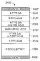
- quantum dot layer 2101is sandwiched between a layer 2103 of n-type GaN and a layer 2105 of p-type GaN.
- layer 2103can be comprised of n-type InGaN and layer 2105 can be comprised of p-type InGaN.
- Adjacent to n-type GaN layer 2103 (or n-type InGaN)is a layer 2107 of n-type AlGaN.
- Adjacent to p-type GaN layer 2105 (or p-type InGaN)is a layer 2109 of p-type AlGaN.
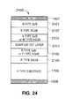
- devices 2200 and 2400utilize p-type substrate 1709 (e.g., p-type SiC).
- FIGS. 23 and 24are the same as those shown in FIGS. 21 and 22 with the addition of a narrow band gap material layer (i.e., layers 2301 and 2401 , respectively) interposed between the outermost wide band gap layer and contact 1007 .
- a narrow band gap material layeri.e., layers 2301 and 2401 , respectively
- the inclusion of such a layeris advantageous due to the low voltage drop incurred by the device.
Landscapes
- Engineering & Computer Science (AREA)
- Chemical & Material Sciences (AREA)
- Physics & Mathematics (AREA)
- Condensed Matter Physics & Semiconductors (AREA)
- General Physics & Mathematics (AREA)
- Manufacturing & Machinery (AREA)
- Computer Hardware Design (AREA)
- Microelectronics & Electronic Packaging (AREA)
- Power Engineering (AREA)
- Crystallography & Structural Chemistry (AREA)
- Materials Engineering (AREA)
- Metallurgy (AREA)
- Organic Chemistry (AREA)
- Nanotechnology (AREA)
- Inorganic Chemistry (AREA)
- Mathematical Physics (AREA)
- Theoretical Computer Science (AREA)
- Chemical Kinetics & Catalysis (AREA)
- General Chemical & Material Sciences (AREA)
- Composite Materials (AREA)
- Led Devices (AREA)
Abstract
Description
Claims (51)
Priority Applications (1)
| Application Number | Priority Date | Filing Date | Title |
|---|---|---|---|
| US09/861,180US6479839B2 (en) | 1997-11-18 | 2001-05-18 | III-V compounds semiconductor device with an AlxByInzGa1-x-y-zN non continuous quantum dot layer |
Applications Claiming Priority (4)
| Application Number | Priority Date | Filing Date | Title |
|---|---|---|---|
| US6694097P | 1997-11-18 | 1997-11-18 | |
| US09/195,217US6218269B1 (en) | 1997-11-18 | 1998-11-18 | Process for producing III-V nitride pn junctions and p-i-n junctions |
| US63863800A | 2000-08-14 | 2000-08-14 | |
| US09/861,180US6479839B2 (en) | 1997-11-18 | 2001-05-18 | III-V compounds semiconductor device with an AlxByInzGa1-x-y-zN non continuous quantum dot layer |
Related Parent Applications (1)
| Application Number | Title | Priority Date | Filing Date |
|---|---|---|---|
| US63863800AContinuation-In-Part | 1997-11-18 | 2000-08-14 |
Publications (2)
| Publication Number | Publication Date |
|---|---|
| US20020030192A1 US20020030192A1 (en) | 2002-03-14 |
| US6479839B2true US6479839B2 (en) | 2002-11-12 |
Family
ID=46277639
Family Applications (1)
| Application Number | Title | Priority Date | Filing Date |
|---|---|---|---|
| US09/861,180Expired - LifetimeUS6479839B2 (en) | 1997-11-18 | 2001-05-18 | III-V compounds semiconductor device with an AlxByInzGa1-x-y-zN non continuous quantum dot layer |
Country Status (1)
| Country | Link |
|---|---|
| US (1) | US6479839B2 (en) |
Cited By (13)
| Publication number | Priority date | Publication date | Assignee | Title |
|---|---|---|---|---|
| WO2003038874A1 (en)* | 2001-10-26 | 2003-05-08 | Oriol, Inc. | Diode having vertical structure and method of manufacturing the same |
| WO2003088320A3 (en)* | 2002-04-09 | 2004-02-05 | Oriol Inc | A method of fabricating vertical devices using a metal support film |
| US20040026704A1 (en)* | 1997-11-18 | 2004-02-12 | Technologies & Devices Int.'s Inc. | III-V compound semiconductor device with an AIxByInzGa1-x-y-zN1-a-bPaAsb non-continuous quantum dot layer |
| US6841802B2 (en)* | 2002-06-26 | 2005-01-11 | Oriol, Inc. | Thin film light emitting diode |
| US20050098792A1 (en)* | 2002-04-09 | 2005-05-12 | Jong-Lam Lee | Method of fabricating vertical structure LEDs |
| US20060108591A1 (en)* | 2004-11-19 | 2006-05-25 | Macronix International Co., Ltd. | Method and apparatus for electroluminescence |
| US20070006801A1 (en)* | 2005-07-09 | 2007-01-11 | Stringfellow Gerald B | Use of surfactants to control unintentional dopant in semiconductors |
| US20070108466A1 (en)* | 2005-08-31 | 2007-05-17 | University Of Florida Research Foundation, Inc. | Group III-nitrides on Si substrates using a nanostructured interlayer |
| US20070215857A1 (en)* | 2001-07-10 | 2007-09-20 | Nec Corporation | Semiconductor quantum dot device |
| US20100065816A1 (en)* | 2003-07-18 | 2010-03-18 | Seong Jae Kim | Light emitting diode and fabrication method thereof |
| US20110042683A1 (en)* | 2006-08-29 | 2011-02-24 | University Of Florida Research Foundation, Inc. | Crack free multilayered devices, methods of manufacture thereof and articles comprising the same |
| US8647435B1 (en) | 2006-10-11 | 2014-02-11 | Ostendo Technologies, Inc. | HVPE apparatus and methods for growth of p-type single crystal group III nitride materials |
| US11661673B1 (en) | 2006-03-27 | 2023-05-30 | Ostendo Technologies, Inc. | HVPE apparatus and methods for growing indium nitride and indium nitride materials and structures grown thereby |
Families Citing this family (4)
| Publication number | Priority date | Publication date | Assignee | Title |
|---|---|---|---|---|
| US6504183B1 (en)* | 2000-09-08 | 2003-01-07 | United Epitaxy Company | Epitaxial growth of nitride semiconductor device |
| CN109225297B (en)* | 2018-09-29 | 2021-08-17 | 台州学院 | A composite catalyst QDs-SISCN and its preparation method and application |
| CN110488358B (en) | 2019-08-23 | 2020-10-16 | 清华大学 | Moving and fixed source combined transient electromagnetic detector for unexploded bomb and detection method thereof |
| CN110488356B (en) | 2019-08-23 | 2020-08-21 | 清华大学 | Combined detection method of transient electromagnetic and magnetic field gradients for unexploded bombs |
Citations (46)
| Publication number | Priority date | Publication date | Assignee | Title |
|---|---|---|---|---|
| US3683240A (en) | 1971-07-22 | 1972-08-08 | Rca Corp | ELECTROLUMINESCENT SEMICONDUCTOR DEVICE OF GaN |
| US3819974A (en) | 1973-03-12 | 1974-06-25 | D Stevenson | Gallium nitride metal-semiconductor junction light emitting diode |
| US3849707A (en) | 1973-03-07 | 1974-11-19 | Ibm | PLANAR GaN ELECTROLUMINESCENT DEVICE |
| US3922703A (en) | 1974-04-03 | 1975-11-25 | Rca Corp | Electroluminescent semiconductor device |
| US4095331A (en) | 1976-11-04 | 1978-06-20 | The United States Of America As Represented By The Secretary Of The Air Force | Fabrication of an epitaxial layer diode in aluminum nitride on sapphire |
| US4144116A (en) | 1975-03-19 | 1979-03-13 | U.S. Philips Corporation | Vapor deposition of single crystal gallium nitride |
| US4268842A (en) | 1976-09-06 | 1981-05-19 | U.S. Philips Corporation | Electroluminescent gallium nitride semiconductor device |
| US4396929A (en) | 1979-10-19 | 1983-08-02 | Matsushita Electric Industrial Company, Ltd. | Gallium nitride light-emitting element and method of manufacturing the same |
| US4918497A (en) | 1988-12-14 | 1990-04-17 | Cree Research, Inc. | Blue light emitting diode formed in silicon carbide |
| US4966862A (en) | 1989-08-28 | 1990-10-30 | Cree Research, Inc. | Method of production of light emitting diodes |
| US5061972A (en) | 1988-12-14 | 1991-10-29 | Cree Research, Inc. | Fast recovery high temperature rectifying diode formed in silicon carbide |
| US5210051A (en) | 1990-03-27 | 1993-05-11 | Cree Research, Inc. | High efficiency light emitting diodes from bipolar gallium nitride |
| US5243204A (en) | 1990-05-18 | 1993-09-07 | Sharp Kabushiki Kaisha | Silicon carbide light emitting diode and a method for the same |
| US5264713A (en) | 1991-06-14 | 1993-11-23 | Cree Research, Inc. | Junction field-effect transistor formed in silicon carbide |
| US5270554A (en) | 1991-06-14 | 1993-12-14 | Cree Research, Inc. | High power high frequency metal-semiconductor field-effect transistor formed in silicon carbide |
| US5290393A (en) | 1991-01-31 | 1994-03-01 | Nichia Kagaku Kogyo K.K. | Crystal growth method for gallium nitride-based compound semiconductor |
| US5306662A (en) | 1991-11-08 | 1994-04-26 | Nichia Chemical Industries, Ltd. | Method of manufacturing P-type compound semiconductor |
| US5338994A (en) | 1989-07-20 | 1994-08-16 | General Electric Company | Method and apparatus for achieving current balance in parallel connected switching devices |
| US5387804A (en) | 1988-12-28 | 1995-02-07 | Sharp Kabushiki Kaisha | Light emitting diode |
| USRE34861E (en) | 1987-10-26 | 1995-02-14 | North Carolina State University | Sublimation of silicon carbide to produce large, device quality single crystals of silicon carbide |
| US5393993A (en) | 1993-12-13 | 1995-02-28 | Cree Research, Inc. | Buffer structure between silicon carbide and gallium nitride and resulting semiconductor devices |
| US5416342A (en) | 1993-06-23 | 1995-05-16 | Cree Research, Inc. | Blue light-emitting diode with high external quantum efficiency |
| US5432808A (en) | 1993-03-15 | 1995-07-11 | Kabushiki Kaisha Toshiba | Compound semicondutor light-emitting device |
| US5433169A (en) | 1990-10-25 | 1995-07-18 | Nichia Chemical Industries, Ltd. | Method of depositing a gallium nitride-based III-V group compound semiconductor crystal layer |
| US5506421A (en) | 1992-11-24 | 1996-04-09 | Cree Research, Inc. | Power MOSFET in silicon carbide |
| US5523589A (en) | 1994-09-20 | 1996-06-04 | Cree Research, Inc. | Vertical geometry light emitting diode with group III nitride active layer and extended lifetime |
| US5539217A (en) | 1993-08-09 | 1996-07-23 | Cree Research, Inc. | Silicon carbide thyristor |
| US5563422A (en) | 1993-04-28 | 1996-10-08 | Nichia Chemical Industries, Ltd. | Gallium nitride-based III-V group compound semiconductor device and method of producing the same |
| US5578839A (en) | 1992-11-20 | 1996-11-26 | Nichia Chemical Industries, Ltd. | Light-emitting gallium nitride-based compound semiconductor device |
| US5585648A (en) | 1995-02-03 | 1996-12-17 | Tischler; Michael A. | High brightness electroluminescent device, emitting in the green to ultraviolet spectrum, and method of making the same |
| US5604135A (en) | 1994-08-12 | 1997-02-18 | Cree Research, Inc. | Method of forming green light emitting diode in silicon carbide |
| US5620557A (en) | 1993-12-27 | 1997-04-15 | Toyoda Gosei Co., Ltd. | Sapphireless group III nitride semiconductor and method for making same |
| US5650641A (en) | 1994-09-01 | 1997-07-22 | Toyoda Gosei Co., Ltd. | Semiconductor device having group III nitride compound and enabling control of emission color, and flat display comprising such device |
| US5661074A (en) | 1995-02-03 | 1997-08-26 | Advanced Technology Materials, Inc. | High brightness electroluminescent device emitting in the green to ultraviolet spectrum and method of making the same |
| US5679153A (en) | 1994-11-30 | 1997-10-21 | Cree Research, Inc. | Method for reducing micropipe formation in the epitaxial growth of silicon carbide and resulting silicon carbide structures |
| US5718760A (en) | 1996-02-05 | 1998-02-17 | Cree Research, Inc. | Growth of colorless silicon carbide crystals |
| US5739554A (en) | 1995-05-08 | 1998-04-14 | Cree Research, Inc. | Double heterojunction light emitting diode with gallium nitride active layer |
| US5767533A (en) | 1996-05-08 | 1998-06-16 | Vydyanath; Honnavalli R. | High-conductivity semiconductor material having a dopant comprising coulombic pairs of elements |
| US5777350A (en) | 1994-12-02 | 1998-07-07 | Nichia Chemical Industries, Ltd. | Nitride semiconductor light-emitting device |
| US5831288A (en) | 1996-06-06 | 1998-11-03 | Cree Research, Inc. | Silicon carbide metal-insulator semiconductor field effect transistor |
| US5846844A (en) | 1993-11-29 | 1998-12-08 | Toyoda Gosei Co., Ltd. | Method for producing group III nitride compound semiconductor substrates using ZnO release layers |
| US5874747A (en) | 1996-02-05 | 1999-02-23 | Advanced Technology Materials, Inc. | High brightness electroluminescent device emitting in the green to ultraviolet spectrum and method of making the same |
| US5888886A (en) | 1997-06-30 | 1999-03-30 | Sdl, Inc. | Method of doping gan layers p-type for device fabrication |
| US5959307A (en) | 1995-11-06 | 1999-09-28 | Nichia Chemical Industries Ltd. | Nitride semiconductor device |
| US5993542A (en) | 1996-12-05 | 1999-11-30 | Sony Corporation | Method for growing nitride III-V compound semiconductor layers and method for fabricating a nitride III-V compound semiconductor substrate |
| US6084899A (en) | 1994-09-14 | 2000-07-04 | Rohm Co. Ltd. | Semiconductor light emitting device and manufacturing method |
- 2001
- 2001-05-18USUS09/861,180patent/US6479839B2/ennot_activeExpired - Lifetime
Patent Citations (54)
| Publication number | Priority date | Publication date | Assignee | Title |
|---|---|---|---|---|
| US3683240A (en) | 1971-07-22 | 1972-08-08 | Rca Corp | ELECTROLUMINESCENT SEMICONDUCTOR DEVICE OF GaN |
| US3849707A (en) | 1973-03-07 | 1974-11-19 | Ibm | PLANAR GaN ELECTROLUMINESCENT DEVICE |
| US3819974A (en) | 1973-03-12 | 1974-06-25 | D Stevenson | Gallium nitride metal-semiconductor junction light emitting diode |
| US3922703A (en) | 1974-04-03 | 1975-11-25 | Rca Corp | Electroluminescent semiconductor device |
| US4144116A (en) | 1975-03-19 | 1979-03-13 | U.S. Philips Corporation | Vapor deposition of single crystal gallium nitride |
| US4268842A (en) | 1976-09-06 | 1981-05-19 | U.S. Philips Corporation | Electroluminescent gallium nitride semiconductor device |
| US4095331A (en) | 1976-11-04 | 1978-06-20 | The United States Of America As Represented By The Secretary Of The Air Force | Fabrication of an epitaxial layer diode in aluminum nitride on sapphire |
| US4396929A (en) | 1979-10-19 | 1983-08-02 | Matsushita Electric Industrial Company, Ltd. | Gallium nitride light-emitting element and method of manufacturing the same |
| USRE34861E (en) | 1987-10-26 | 1995-02-14 | North Carolina State University | Sublimation of silicon carbide to produce large, device quality single crystals of silicon carbide |
| US5061972A (en) | 1988-12-14 | 1991-10-29 | Cree Research, Inc. | Fast recovery high temperature rectifying diode formed in silicon carbide |
| US4918497A (en) | 1988-12-14 | 1990-04-17 | Cree Research, Inc. | Blue light emitting diode formed in silicon carbide |
| US5387804A (en) | 1988-12-28 | 1995-02-07 | Sharp Kabushiki Kaisha | Light emitting diode |
| US5338994A (en) | 1989-07-20 | 1994-08-16 | General Electric Company | Method and apparatus for achieving current balance in parallel connected switching devices |
| US4966862A (en) | 1989-08-28 | 1990-10-30 | Cree Research, Inc. | Method of production of light emitting diodes |
| US5210051A (en) | 1990-03-27 | 1993-05-11 | Cree Research, Inc. | High efficiency light emitting diodes from bipolar gallium nitride |
| US5243204A (en) | 1990-05-18 | 1993-09-07 | Sharp Kabushiki Kaisha | Silicon carbide light emitting diode and a method for the same |
| US5433169A (en) | 1990-10-25 | 1995-07-18 | Nichia Chemical Industries, Ltd. | Method of depositing a gallium nitride-based III-V group compound semiconductor crystal layer |
| US5290393A (en) | 1991-01-31 | 1994-03-01 | Nichia Kagaku Kogyo K.K. | Crystal growth method for gallium nitride-based compound semiconductor |
| US5264713A (en) | 1991-06-14 | 1993-11-23 | Cree Research, Inc. | Junction field-effect transistor formed in silicon carbide |
| US5270554A (en) | 1991-06-14 | 1993-12-14 | Cree Research, Inc. | High power high frequency metal-semiconductor field-effect transistor formed in silicon carbide |
| US5306662A (en) | 1991-11-08 | 1994-04-26 | Nichia Chemical Industries, Ltd. | Method of manufacturing P-type compound semiconductor |
| US5468678A (en) | 1991-11-08 | 1995-11-21 | Nichia Chemical Industries, Ltd. | Method of manufacturing P-type compound semiconductor |
| US5747832A (en) | 1992-11-20 | 1998-05-05 | Nichia Chemical Industries, Ltd. | Light-emitting gallium nitride-based compound semiconductor device |
| US5734182A (en) | 1992-11-20 | 1998-03-31 | Nichia Chemical Industries Ltd. | Light-emitting gallium nitride-based compound semiconducor device |
| US5578839A (en) | 1992-11-20 | 1996-11-26 | Nichia Chemical Industries, Ltd. | Light-emitting gallium nitride-based compound semiconductor device |
| US5880486A (en) | 1992-11-20 | 1999-03-09 | Nichia Chemical Industries, Ltd. | Light-emitting gallium nitride-based compound semiconductor device |
| US5506421A (en) | 1992-11-24 | 1996-04-09 | Cree Research, Inc. | Power MOSFET in silicon carbide |
| US5432808A (en) | 1993-03-15 | 1995-07-11 | Kabushiki Kaisha Toshiba | Compound semicondutor light-emitting device |
| US5652434A (en) | 1993-04-28 | 1997-07-29 | Nichia Chemical Industries, Ltd. | Gallium nitride-based III-V group compound semiconductor |
| US5877558A (en) | 1993-04-28 | 1999-03-02 | Nichia Chemical Industries, Ltd. | Gallium nitride-based III-V group compound semiconductor |
| US5563422A (en) | 1993-04-28 | 1996-10-08 | Nichia Chemical Industries, Ltd. | Gallium nitride-based III-V group compound semiconductor device and method of producing the same |
| US5767581A (en) | 1993-04-28 | 1998-06-16 | Nichia Chemical Industries, Ltd. | Gallium nitride-based III-V group compound semiconductor |
| US5416342A (en) | 1993-06-23 | 1995-05-16 | Cree Research, Inc. | Blue light-emitting diode with high external quantum efficiency |
| US5539217A (en) | 1993-08-09 | 1996-07-23 | Cree Research, Inc. | Silicon carbide thyristor |
| US5846844A (en) | 1993-11-29 | 1998-12-08 | Toyoda Gosei Co., Ltd. | Method for producing group III nitride compound semiconductor substrates using ZnO release layers |
| US5393993A (en) | 1993-12-13 | 1995-02-28 | Cree Research, Inc. | Buffer structure between silicon carbide and gallium nitride and resulting semiconductor devices |
| US5620557A (en) | 1993-12-27 | 1997-04-15 | Toyoda Gosei Co., Ltd. | Sapphireless group III nitride semiconductor and method for making same |
| US5604135A (en) | 1994-08-12 | 1997-02-18 | Cree Research, Inc. | Method of forming green light emitting diode in silicon carbide |
| US5650641A (en) | 1994-09-01 | 1997-07-22 | Toyoda Gosei Co., Ltd. | Semiconductor device having group III nitride compound and enabling control of emission color, and flat display comprising such device |
| US6115399A (en) | 1994-09-14 | 2000-09-05 | Rohm Co. Ltd. | Semiconductor light emitting device |
| US6084899A (en) | 1994-09-14 | 2000-07-04 | Rohm Co. Ltd. | Semiconductor light emitting device and manufacturing method |
| US5523589A (en) | 1994-09-20 | 1996-06-04 | Cree Research, Inc. | Vertical geometry light emitting diode with group III nitride active layer and extended lifetime |
| US5679153A (en) | 1994-11-30 | 1997-10-21 | Cree Research, Inc. | Method for reducing micropipe formation in the epitaxial growth of silicon carbide and resulting silicon carbide structures |
| US5777350A (en) | 1994-12-02 | 1998-07-07 | Nichia Chemical Industries, Ltd. | Nitride semiconductor light-emitting device |
| US5661074A (en) | 1995-02-03 | 1997-08-26 | Advanced Technology Materials, Inc. | High brightness electroluminescent device emitting in the green to ultraviolet spectrum and method of making the same |
| US5585648A (en) | 1995-02-03 | 1996-12-17 | Tischler; Michael A. | High brightness electroluminescent device, emitting in the green to ultraviolet spectrum, and method of making the same |
| US5739554A (en) | 1995-05-08 | 1998-04-14 | Cree Research, Inc. | Double heterojunction light emitting diode with gallium nitride active layer |
| US5959307A (en) | 1995-11-06 | 1999-09-28 | Nichia Chemical Industries Ltd. | Nitride semiconductor device |
| US5718760A (en) | 1996-02-05 | 1998-02-17 | Cree Research, Inc. | Growth of colorless silicon carbide crystals |
| US5874747A (en) | 1996-02-05 | 1999-02-23 | Advanced Technology Materials, Inc. | High brightness electroluminescent device emitting in the green to ultraviolet spectrum and method of making the same |
| US5767533A (en) | 1996-05-08 | 1998-06-16 | Vydyanath; Honnavalli R. | High-conductivity semiconductor material having a dopant comprising coulombic pairs of elements |
| US5831288A (en) | 1996-06-06 | 1998-11-03 | Cree Research, Inc. | Silicon carbide metal-insulator semiconductor field effect transistor |
| US5993542A (en) | 1996-12-05 | 1999-11-30 | Sony Corporation | Method for growing nitride III-V compound semiconductor layers and method for fabricating a nitride III-V compound semiconductor substrate |
| US5888886A (en) | 1997-06-30 | 1999-03-30 | Sdl, Inc. | Method of doping gan layers p-type for device fabrication |
Non-Patent Citations (18)
| Title |
|---|
| Agarwal, A.K., et al., "SiC Power Devices", Naval Research Reviews, vol. 51, No. 1, 1999, pp. 13-23. |
| Akasaki, I., et al. "Widegap Column-III Nitride Semiconductors for UV/Blue Light Emitting Devices", J. Electrochem. Soc. vol. 141, No. 8, Aug., 1994, pp. 2266-2271. |
| Akasaki, I., et al., "Photoluminescence of Mg-doped p-type GaN and electroluminescence of GaN p-n junction LED", Journal of Luminescence 48 & 49 (1991), pp. 666-670. |
| Bahng, W., et al. "Rapid enlargement of SiC single crystal using a cone-shaped platform", Journal of Crystal Growth, 209 (2000), pp. 767-772. |
| Choyke, W.J., et al., "SiC-The Power Semiconductor for the 21st Century: A Materials Perspective", Naval Research Reviews, vol. 51, No. 1, 1999, pp. 2-12. |
| Choyke, W.J., et al., "SiC—The Power Semiconductor for the 21st Century: A Materials Perspective", Naval Research Reviews, vol. 51, No. 1, 1999, pp. 2-12. |
| Detchprohm, T., et al., "The homoepitaxy of GaN by metalorganic vapor phase epitaxy using GaN substrates", Journal of Crystal Growth, 137 (1994), pp. 170-174. |
| Khan, M.A., et al., "Violet-blue GaN homojunction light emitting diodes with rapid thermal annealed p-type layers", Appl. Phys. Lett., vol. 66, No. 16, Apr. 17, 1995, pp. 2046-2047. |
| Koleske, D.D., et al. "GaN-Based Materials Growth for Microwave Electronic Device Applications", Naval Research Reviews, vol. 51 No. 1, 1999. pp. 61-71. |
| Linthicum, K., et al., "Recent Progress in the Growth and the Control of Defects and Electronic Properties in III-Nitride Thin Films", Naval Research Reviews, vol. 51, No. 1, 1999, pp. 44-53. |
| Maruska, H.P., et al.,"Violet Luminescence of Mg-doped GaN", Appl. Phys. Lett., vol. 22, No. 6, Mar. 15, 1973, pp. 303-305. |
| Masatoshi, S., et al., "Epitaxial Growth of Undoped and Mg-Doped GaN", Japanese Journal of Appl. Physics, vol. 15, No. 10, Oct,, 1976, pp. 1943-1950. |
| Melnik, Y.V., et all, "High-guality GaN grown directly on SiC by halide vapour phase epitaxy", Inst. Phys. Conf. Ser. No. 142, Chapter 5 (1995), pp. 863-866. |
| Mishra, U.K., et al., "Gallium Nitride-Based Solutions for Communications and Sensing", Naval Research Reviews, vol. 51, No. 1, 1999, pp. 54-60. |
| Morkoc, H., "GaN-Based Modulation-Doped FETs and UV Detectors", Naval Research Reviews, vol. 51, No. 1, 1999, pp. 24-43. |
| Nakamura, S., et al., "Highly P-Typed Mg-Doped GaN Films Grown with GaN Buffer Layers", Jpn. J. Appl. Phys., vol. 30, No. 10A, Oct., 1991, pp. L1708-L1711. |
| Nakamura, S., et al., "High-Power GaN P-N Junction Blue-Light-Emitting Diodes", Japanese Journal of Appl. Physics, vol. 30, No. 12A, Dec. 1991, pp. L1999-L2001. |
| Steigerwald, D., et al., "III-V Nitride Semiconductors for High-Performance Blue and Green Light-Emitting Devices", JOM, 49 (9), 1997, pp. 18-23. |
Cited By (99)
| Publication number | Priority date | Publication date | Assignee | Title |
|---|---|---|---|---|
| US6849862B2 (en)* | 1997-11-18 | 2005-02-01 | Technologies And Devices International, Inc. | III-V compound semiconductor device with an AlxByInzGa1-x-y-zN1-a-bPaAsb non-continuous quantum dot layer |
| US20040026704A1 (en)* | 1997-11-18 | 2004-02-12 | Technologies & Devices Int.'s Inc. | III-V compound semiconductor device with an AIxByInzGa1-x-y-zN1-a-bPaAsb non-continuous quantum dot layer |
| US20070215857A1 (en)* | 2001-07-10 | 2007-09-20 | Nec Corporation | Semiconductor quantum dot device |
| US8106378B2 (en)* | 2001-07-10 | 2012-01-31 | Nec Corporation | Semiconductor quantum dot device |
| US20060091420A1 (en)* | 2001-10-26 | 2006-05-04 | Yoo Myung C | Diode having vertical structure and method of manufacturing the same |
| US20110049470A1 (en)* | 2001-10-26 | 2011-03-03 | Yoo Myung Cheol | Diode having vertical structure and method of manufacturing the same |
| US9620677B2 (en) | 2001-10-26 | 2017-04-11 | Lg Innotek Co., Ltd. | Diode having vertical structure |
| WO2003038874A1 (en)* | 2001-10-26 | 2003-05-08 | Oriol, Inc. | Diode having vertical structure and method of manufacturing the same |
| US7371597B2 (en) | 2001-10-26 | 2008-05-13 | Lg Electronics Inc. | Diode having vertical structure and method of manufacturing the same |
| US8008681B2 (en) | 2001-10-26 | 2011-08-30 | Lg Electronics Inc. | Diode having vertical structure and method of manufacturing the same |
| US7915632B2 (en) | 2001-10-26 | 2011-03-29 | Lg Electronics Inc. | Diode having vertical structure and method of manufacturing the same |
| US8592846B2 (en) | 2001-10-26 | 2013-11-26 | Lg Electronics Inc. | Diode having vertical structure and method of manufacturing the same |
| US7148520B2 (en) | 2001-10-26 | 2006-12-12 | Lg Electronics Inc. | Diode having vertical structure and method of manufacturing the same |
| US10032959B2 (en) | 2001-10-26 | 2018-07-24 | Lg Innotek Co., Ltd. | Diode having vertical structure |
| US20070057273A1 (en)* | 2001-10-26 | 2007-03-15 | Yoo Myung C | Diode having vertical structure and method of manufacturing the same |
| US7863638B2 (en) | 2001-10-26 | 2011-01-04 | Lg Electroncis Inc. | Diode having vertical structure and method of manufacturing the same |
| US7821021B2 (en) | 2001-10-26 | 2010-10-26 | Lg Electronics Inc. | Diode having vertical structure and method of manufacturing the same |
| US10326055B2 (en) | 2001-10-26 | 2019-06-18 | Lg Innotek Co., Ltd. | Diode having vertical structure |
| US9000468B2 (en) | 2001-10-26 | 2015-04-07 | Lg Innotek Co., Ltd. | Diode having vertical structure |
| US7772020B2 (en) | 2002-04-09 | 2010-08-10 | Lg Electronics Inc. | Method of fabricating vertical devices using a metal support film |
| US20100308368A1 (en)* | 2002-04-09 | 2010-12-09 | Jong-Lam Lee | Method of fabricating vertical structure leds |
| US20080064132A1 (en)* | 2002-04-09 | 2008-03-13 | Yoo Myung C | Method of fabricating vertical devices using a metal support film |
| US10453993B1 (en) | 2002-04-09 | 2019-10-22 | Lg Innotek Co., Ltd. | Vertical structure LEDs |
| WO2003088320A3 (en)* | 2002-04-09 | 2004-02-05 | Oriol Inc | A method of fabricating vertical devices using a metal support film |
| US10453998B2 (en) | 2002-04-09 | 2019-10-22 | Lg Innotek Co. Ltd. | Vertical topology light emitting device |
| US7250638B2 (en) | 2002-04-09 | 2007-07-31 | Lg Electronics Inc. | Method of fabricating vertical structure LEDs |
| US7462881B2 (en) | 2002-04-09 | 2008-12-09 | Lg Electronics Inc. | Method of fabricating vertical structure LEDs |
| US7563629B2 (en) | 2002-04-09 | 2009-07-21 | Lg Electronics Inc. | Method of fabricating vertical structure LEDs |
| US7569865B2 (en) | 2002-04-09 | 2009-08-04 | Lg Electronics Inc. | Method of fabricating vertical structure LEDs |
| US7576368B2 (en) | 2002-04-09 | 2009-08-18 | Lg Electronics Inc. | Method of fabricating vertical structure LEDs |
| US7588952B2 (en) | 2002-04-09 | 2009-09-15 | Lg Electronics Inc. | Method of fabricating vertical structure LEDs |
| US20090278161A1 (en)* | 2002-04-09 | 2009-11-12 | Jong-Lam Lee | Method of fabricating vertical structure LEDs |
| US20080001166A1 (en)* | 2002-04-09 | 2008-01-03 | Jong-Lam Lee | Method of fabricating vertical structure leds |
| US9209360B2 (en) | 2002-04-09 | 2015-12-08 | Lg Innotek Co., Ltd. | Vertical topology light-emitting device |
| US10243101B2 (en) | 2002-04-09 | 2019-03-26 | Lg Innotek Co., Ltd. | Vertical structure LEDs |
| US8896017B2 (en) | 2002-04-09 | 2014-11-25 | Lg Innotek Co., Ltd. | Vertical structure LEDs |
| US10147847B2 (en) | 2002-04-09 | 2018-12-04 | Lg Innotek Co., Ltd. | Vertical topology light emitting device |
| US9000477B2 (en) | 2002-04-09 | 2015-04-07 | Lg Innotek Co., Ltd. | Vertical topology light-emitting device |
| US7816705B2 (en) | 2002-04-09 | 2010-10-19 | Lg Electronics Inc. | Method of fabricating vertical structure LEDs |
| US10461217B2 (en) | 2002-04-09 | 2019-10-29 | Lg Innotek Co., Ltd. | Vertical structure LEDs |
| US8384120B2 (en) | 2002-04-09 | 2013-02-26 | Lg Electronics Inc. | Method of fabricating vertical structure LEDs |
| US10600933B2 (en) | 2002-04-09 | 2020-03-24 | Lg Innotek Co., Ltd. | Vertical structure LEDs |
| US10644200B2 (en) | 2002-04-09 | 2020-05-05 | Lg Innotek Co., Ltd. | Vertical topology light emitting device |
| US9882084B2 (en) | 2002-04-09 | 2018-01-30 | Lg Innotek Co., Ltd. | Vertical structure LEDs |
| US20060244001A1 (en)* | 2002-04-09 | 2006-11-02 | Lg Electronic Inc. | Method of fabricating vertical structure LEDs |
| US8809898B2 (en) | 2002-04-09 | 2014-08-19 | Lg Innotek Co., Ltd. | Method of fabricating vertical structure LEDs |
| US7928465B2 (en) | 2002-04-09 | 2011-04-19 | Lg Electronics Inc. | Method of fabricating vertical structure LEDs |
| US9224907B2 (en) | 2002-04-09 | 2015-12-29 | Lg Innotek Co., Ltd. | Vertical structure LEDs |
| US9847455B2 (en) | 2002-04-09 | 2017-12-19 | Lg Innotek Co., Ltd. | Vertical topology light emitting device |
| US20110193128A1 (en)* | 2002-04-09 | 2011-08-11 | Jong Lam Lee | Method of fabricating vertical structure leds |
| US20060099730A1 (en)* | 2002-04-09 | 2006-05-11 | Lg Electronics Inc. | Method of fabricating vertical structure LEDs |
| US8669587B2 (en) | 2002-04-09 | 2014-03-11 | Lg Innotek Co., Ltd. | Vertical topology light emitting device |
| US8022386B2 (en) | 2002-04-09 | 2011-09-20 | Lg Electronics Inc. | Vertical topology light emitting device |
| US8106417B2 (en) | 2002-04-09 | 2012-01-31 | Lg Electronics Inc. | Vertical topology light emitting device using a conductive support structure |
| US20060071230A1 (en)* | 2002-04-09 | 2006-04-06 | Lg Electronics Inc. | Method of fabricating vertical structure LEDs |
| US9472727B2 (en) | 2002-04-09 | 2016-10-18 | Lg Innotek Co., Ltd. | Vertical structure LEDs |
| US20050098792A1 (en)* | 2002-04-09 | 2005-05-12 | Jong-Lam Lee | Method of fabricating vertical structure LEDs |
| US9478709B2 (en) | 2002-04-09 | 2016-10-25 | Lg Innotek Co., Ltd. | Vertical topology light emitting device |
| US8564016B2 (en) | 2002-04-09 | 2013-10-22 | Lg Electronics Inc. | Vertical topology light emitting device |
| US8294172B2 (en) | 2002-04-09 | 2012-10-23 | Lg Electronics Inc. | Method of fabricating vertical devices using a metal support film |
| US8368115B2 (en) | 2002-04-09 | 2013-02-05 | Lg Electronics Inc. | Method of fabricating vertical devices using a metal support film |
| US7649210B2 (en) | 2002-06-26 | 2010-01-19 | Lg Electronics Inc. | Thin film light emitting diode |
| US8384091B2 (en) | 2002-06-26 | 2013-02-26 | Lg Electronics Inc. | Thin film light emitting diode |
| US8445921B2 (en) | 2002-06-26 | 2013-05-21 | Lg Electronics, Inc. | Thin film light emitting diode |
| US8288787B2 (en) | 2002-06-26 | 2012-10-16 | Lg Electronics, Inc. | Thin film light emitting diode |
| US20050093004A1 (en)* | 2002-06-26 | 2005-05-05 | Yoo Myung C. | Thin film light emitting diode |
| US8207552B2 (en) | 2002-06-26 | 2012-06-26 | Lg Electronics Inc. | Thin film light emitting diode |
| US9716213B2 (en) | 2002-06-26 | 2017-07-25 | Lg Innotek Co., Ltd. | Thin film light emitting diode |
| US9281454B2 (en) | 2002-06-26 | 2016-03-08 | Lg Innotek Co., Ltd. | Thin film light emitting diode |
| US7956364B2 (en) | 2002-06-26 | 2011-06-07 | Lg Electronics Inc. | Thin film light emitting diode |
| US10825962B2 (en) | 2002-06-26 | 2020-11-03 | Lg Innotek Co., Ltd. | Thin film light emitting diode |
| US7691650B2 (en) | 2002-06-26 | 2010-04-06 | Lg Electronics Inc. | Thin film light emitting diode |
| US6841802B2 (en)* | 2002-06-26 | 2005-01-11 | Oriol, Inc. | Thin film light emitting diode |
| US10326059B2 (en) | 2002-06-26 | 2019-06-18 | Lg Innotek Co., Ltd. | Thin film light emitting diode |
| US20080128733A1 (en)* | 2002-06-26 | 2008-06-05 | Yoo Myung Cheol | Thin film light emitting diode |
| US8927960B2 (en) | 2003-07-18 | 2015-01-06 | Lg Innotek Co., Ltd. | Gallium nitride based light emitting diode |
| US20100136732A1 (en)* | 2003-07-18 | 2010-06-03 | Seong Jae Kim | Light emitting diode and fabrication method thereof |
| US8680571B2 (en) | 2003-07-18 | 2014-03-25 | Lg Innotek Co., Ltd. | Gallium nitride based light emitting diode |
| US8674337B2 (en) | 2003-07-18 | 2014-03-18 | Lg Innotek Co., Ltd. | Gallium nitride based light emitting diode and fabrication method thereof |
| US9362454B2 (en) | 2003-07-18 | 2016-06-07 | Lg Innotek Co., Ltd. | Gallium nitride based light emitting diode |
| US7989235B2 (en)* | 2003-07-18 | 2011-08-02 | Lg Innotek Co., Ltd | Light emitting diode and fabrication method thereof |
| US20100065816A1 (en)* | 2003-07-18 | 2010-03-18 | Seong Jae Kim | Light emitting diode and fabrication method thereof |
| US7884388B2 (en)* | 2003-07-18 | 2011-02-08 | Lg Innotek Co., Ltd | Light emitting diode having a first GaN layer and a first semiconductor layer each having a predetermined thickness and fabrication method therof |
| US7230277B2 (en) | 2004-11-19 | 2007-06-12 | Macronix International Co., Ltd. | Method and apparatus for electroluminescence |
| US20060108591A1 (en)* | 2004-11-19 | 2006-05-25 | Macronix International Co., Ltd. | Method and apparatus for electroluminescence |
| US20070218575A1 (en)* | 2004-11-19 | 2007-09-20 | Macronix International Co., Ltd. | Method and Apparatus for Electroluminescence |
| CN100407459C (en)* | 2004-11-19 | 2008-07-30 | 旺宏电子股份有限公司 | Electroluminescent method and device |
| US7439085B2 (en)* | 2004-11-19 | 2008-10-21 | Macronix International Co., Ltd. | Method and apparatus for electroluminescence |
| US20110215275A1 (en)* | 2005-07-09 | 2011-09-08 | The University Of Utah Research Foundation | Methods using surfactants to control unintentional dopant in semiconductors |
| US20070006801A1 (en)* | 2005-07-09 | 2007-01-11 | Stringfellow Gerald B | Use of surfactants to control unintentional dopant in semiconductors |
| US8946674B2 (en) | 2005-08-31 | 2015-02-03 | University Of Florida Research Foundation, Inc. | Group III-nitrides on Si substrates using a nanostructured interlayer |
| US20100029064A1 (en)* | 2005-08-31 | 2010-02-04 | University Of Florida Research Foundation, Inc. | Group iii-nitrides on si substrates using a nanostructured interlayer |
| US20070108466A1 (en)* | 2005-08-31 | 2007-05-17 | University Of Florida Research Foundation, Inc. | Group III-nitrides on Si substrates using a nanostructured interlayer |
| US8268646B2 (en) | 2005-08-31 | 2012-09-18 | University Of Florida Research Foundation, Inc. | Group III-nitrides on SI substrates using a nanostructured interlayer |
| US11661673B1 (en) | 2006-03-27 | 2023-05-30 | Ostendo Technologies, Inc. | HVPE apparatus and methods for growing indium nitride and indium nitride materials and structures grown thereby |
| US20110042683A1 (en)* | 2006-08-29 | 2011-02-24 | University Of Florida Research Foundation, Inc. | Crack free multilayered devices, methods of manufacture thereof and articles comprising the same |
| US8222057B2 (en) | 2006-08-29 | 2012-07-17 | University Of Florida Research Foundation, Inc. | Crack free multilayered devices, methods of manufacture thereof and articles comprising the same |
| US8647435B1 (en) | 2006-10-11 | 2014-02-11 | Ostendo Technologies, Inc. | HVPE apparatus and methods for growth of p-type single crystal group III nitride materials |
| US9416464B1 (en) | 2006-10-11 | 2016-08-16 | Ostendo Technologies, Inc. | Apparatus and methods for controlling gas flows in a HVPE reactor |
Also Published As
| Publication number | Publication date |
|---|---|
| US20020030192A1 (en) | 2002-03-14 |
Similar Documents
| Publication | Publication Date | Title |
|---|---|---|
| US6849862B2 (en) | III-V compound semiconductor device with an AlxByInzGa1-x-y-zN1-a-bPaAsb non-continuous quantum dot layer | |
| US6559038B2 (en) | Method for growing p-n heterojunction-based structures utilizing HVPE techniques | |
| US6555452B2 (en) | Method for growing p-type III-V compound material utilizing HVPE techniques | |
| US6476420B2 (en) | P-N homojunction-based structures utilizing HVPE growth III-V compound layers | |
| US6599133B2 (en) | Method for growing III-V compound semiconductor structures with an integral non-continuous quantum dot layer utilizing HVPE techniques | |
| US6890809B2 (en) | Method for fabricating a P-N heterojunction device utilizing HVPE grown III-V compound layers and resultant device | |
| US6955719B2 (en) | Manufacturing methods for semiconductor devices with multiple III-V material layers | |
| US5432808A (en) | Compound semicondutor light-emitting device | |
| US6479839B2 (en) | III-V compounds semiconductor device with an AlxByInzGa1-x-y-zN non continuous quantum dot layer | |
| US6218269B1 (en) | Process for producing III-V nitride pn junctions and p-i-n junctions | |
| CN100405618C (en) | Light emitting element and method for manufacturing the same | |
| JP5346146B2 (en) | Semiconductor device having selectively doped III-V nitride layer | |
| US4767494A (en) | Preparation process of compound semiconductor | |
| US6559467B2 (en) | P-n heterojunction-based structures utilizing HVPE grown III-V compound layers | |
| JPH06232451A (en) | Method for growing p-type gallium nitride | |
| EP0881666A2 (en) | P-type nitrogen compound semiconductor and method of manufacturing same | |
| US6472300B2 (en) | Method for growing p-n homojunction-based structures utilizing HVPE techniques | |
| US20020017650A1 (en) | III-V compound semiconductor device with an InGaN1-x-yPxASy non-continuous quantum dot layer | |
| JP2000091234A (en) | Manufacture of iii-v nitride compound semiconductor | |
| US6239005B1 (en) | Method of forming epitaxially grown semiconductor layer on metal layer and light emitting semiconductor device comprising said semiconductor layer | |
| US20050009221A1 (en) | Method for manufacturing nitride film including high-resistivity GaN layer and epitaxial substrate manufactured by the method | |
| JPH10290051A (en) | Semiconductor device and manufacturing method thereof | |
| US20020047135A1 (en) | P-N junction-based structures utilizing HVPE grown III-V compound layers | |
| JPH08335715A (en) | Epitaxial wafer and manufacturing method thereof | |
| US7550786B2 (en) | Compound semiconductor epitaxial substrate |
Legal Events
| Date | Code | Title | Description |
|---|---|---|---|
| AS | Assignment | Owner name:FOX GROUP, INC., THE, A CALIFORNIA CORPORATION, CA Free format text:PATENT COLLATERAL ASSIGNMENT AND SECURITY AGREEMENT;ASSIGNOR:TECHNOLOGIES AND DEVICES INTERNATIONAL, INC.;REEL/FRAME:012025/0927 Effective date:20010709 | |
| AS | Assignment | Owner name:TECHNOLOGIES AND DEVICES INTERNATIONAL, INC., MARY Free format text:ASSIGNMENT OF ASSIGNORS INTEREST;ASSIGNORS:NIKOLAEV, AUDREY E.;MELNIK, YURI V.;VASSILEVSKI, KONSTANTIN V.;AND OTHERS;REEL/FRAME:012268/0838;SIGNING DATES FROM 20010902 TO 20010925 | |
| STCF | Information on status: patent grant | Free format text:PATENTED CASE | |
| CC | Certificate of correction | ||
| FPAY | Fee payment | Year of fee payment:4 | |
| FPAY | Fee payment | Year of fee payment:8 | |
| AS | Assignment | Owner name:FOX GROUP, INC., THE, VIRGINIA Free format text:ASSIGNMENT OF ASSIGNORS INTEREST;ASSIGNOR:TECHNOLOGIES AND DEVICES INTERNATIONAL, INC.;REEL/FRAME:025204/0880 Effective date:20100826 | |
| AS | Assignment | Owner name:KYMA TECHNOLOGIES, INC., NORTH CAROLINA Free format text:ASSIGNMENT OF ASSIGNORS INTEREST;ASSIGNOR:THE FOX GROUP, INC.;REEL/FRAME:029632/0347 Effective date:20130109 | |
| FEPP | Fee payment procedure | Free format text:PAYER NUMBER DE-ASSIGNED (ORIGINAL EVENT CODE: RMPN); ENTITY STATUS OF PATENT OWNER: SMALL ENTITY Free format text:PAYOR NUMBER ASSIGNED (ORIGINAL EVENT CODE: ASPN); ENTITY STATUS OF PATENT OWNER: SMALL ENTITY | |
| FPAY | Fee payment | Year of fee payment:12 |