US6479341B1 - Capacitor over metal DRAM structure - Google Patents
Capacitor over metal DRAM structureDownload PDFInfo
- Publication number
- US6479341B1 US6479341B1US09/033,102US3310298AUS6479341B1US 6479341 B1US6479341 B1US 6479341B1US 3310298 AUS3310298 AUS 3310298AUS 6479341 B1US6479341 B1US 6479341B1
- Authority
- US
- United States
- Prior art keywords
- layer
- angstroms
- polysilicon
- insulator layer
- thickness
- Prior art date
- Legal status (The legal status is an assumption and is not a legal conclusion. Google has not performed a legal analysis and makes no representation as to the accuracy of the status listed.)
- Expired - Lifetime
Links
- 229910052751metalInorganic materials0.000titleclaimsabstractdescription98
- 239000002184metalSubstances0.000titleclaimsabstractdescription98
- 239000003990capacitorSubstances0.000titleclaimsabstractdescription35
- 238000000034methodMethods0.000claimsabstractdescription121
- 239000012212insulatorSubstances0.000claimsabstractdescription98
- 229910021420polycrystalline siliconInorganic materials0.000claimsabstractdescription68
- 229920005591polysiliconPolymers0.000claimsabstractdescription68
- 239000004065semiconductorSubstances0.000claimsabstractdescription18
- 239000000758substrateSubstances0.000claimsabstractdescription15
- VYPSYNLAJGMNEJ-UHFFFAOYSA-NSilicium dioxideChemical groupO=[Si]=OVYPSYNLAJGMNEJ-UHFFFAOYSA-N0.000claimsdescription35
- 238000000151depositionMethods0.000claimsdescription32
- 238000004518low pressure chemical vapour depositionMethods0.000claimsdescription27
- WFKWXMTUELFFGS-UHFFFAOYSA-NtungstenChemical compound[W]WFKWXMTUELFFGS-UHFFFAOYSA-N0.000claimsdescription27
- 229910052721tungstenInorganic materials0.000claimsdescription27
- 239000010937tungstenSubstances0.000claimsdescription27
- 229910052814silicon oxideInorganic materials0.000claimsdescription23
- 238000004544sputter depositionMethods0.000claimsdescription21
- 229910052581Si3N4Inorganic materials0.000claimsdescription18
- HQVNEWCFYHHQES-UHFFFAOYSA-Nsilicon nitrideChemical groupN12[Si]34N5[Si]62N3[Si]51N64HQVNEWCFYHHQES-UHFFFAOYSA-N0.000claimsdescription18
- 229910052782aluminiumInorganic materials0.000claimsdescription16
- XAGFODPZIPBFFR-UHFFFAOYSA-NaluminiumChemical compound[Al]XAGFODPZIPBFFR-UHFFFAOYSA-N0.000claimsdescription16
- 230000008021depositionEffects0.000claimsdescription15
- 238000000623plasma-assisted chemical vapour depositionMethods0.000claimsdescription14
- 230000015572biosynthetic processEffects0.000claimsdescription13
- NRTOMJZYCJJWKI-UHFFFAOYSA-NTitanium nitrideChemical compound[Ti]#NNRTOMJZYCJJWKI-UHFFFAOYSA-N0.000claimsdescription12
- XPDWGBQVDMORPB-UHFFFAOYSA-NFluoroformChemical compoundFC(F)FXPDWGBQVDMORPB-UHFFFAOYSA-N0.000claimsdescription9
- 238000005468ion implantationMethods0.000claimsdescription9
- 125000006850spacer groupChemical group0.000claimsdescription9
- 229910052785arsenicInorganic materials0.000claimsdescription8
- RQNWIZPPADIBDY-UHFFFAOYSA-Narsenic atomChemical compound[As]RQNWIZPPADIBDY-UHFFFAOYSA-N0.000claimsdescription8
- QVGXLLKOCUKJST-UHFFFAOYSA-Natomic oxygenChemical compound[O]QVGXLLKOCUKJST-UHFFFAOYSA-N0.000claimsdescription8
- BHEPBYXIRTUNPN-UHFFFAOYSA-Nhydridophosphorus(.) (triplet)Chemical compound[PH]BHEPBYXIRTUNPN-UHFFFAOYSA-N0.000claimsdescription8
- 238000004519manufacturing processMethods0.000claimsdescription8
- 239000001301oxygenSubstances0.000claimsdescription8
- 229910052760oxygenInorganic materials0.000claimsdescription8
- 238000000059patterningMethods0.000claimsdescription8
- 238000011065in-situ storageMethods0.000claimsdescription7
- 235000012239silicon dioxideNutrition0.000claimsdescription7
- 239000000377silicon dioxideSubstances0.000claimsdescription7
- 238000003860storageMethods0.000claimsdescription7
- 230000003647oxidationEffects0.000claimsdescription6
- 238000007254oxidation reactionMethods0.000claimsdescription6
- 229910052710siliconInorganic materials0.000claimsdescription5
- 239000010703siliconSubstances0.000claimsdescription5
- XUIMIQQOPSSXEZ-UHFFFAOYSA-NSiliconChemical compound[Si]XUIMIQQOPSSXEZ-UHFFFAOYSA-N0.000claimsdescription4
- RYGMFSIKBFXOCR-UHFFFAOYSA-NCopperChemical compound[Cu]RYGMFSIKBFXOCR-UHFFFAOYSA-N0.000claimsdescription3
- 239000002131composite materialSubstances0.000claimsdescription3
- 229910052802copperInorganic materials0.000claimsdescription3
- 239000010949copperSubstances0.000claimsdescription3
- PBCFLUZVCVVTBY-UHFFFAOYSA-Ntantalum pentoxideInorganic materialsO=[Ta](=O)O[Ta](=O)=OPBCFLUZVCVVTBY-UHFFFAOYSA-N0.000claimsdescription3
- RTAQQCXQSZGOHL-UHFFFAOYSA-NTitaniumChemical compound[Ti]RTAQQCXQSZGOHL-UHFFFAOYSA-N0.000claimsdescription2
- NMJKIRUDPFBRHW-UHFFFAOYSA-NtitaniumChemical compound[Ti].[Ti]NMJKIRUDPFBRHW-UHFFFAOYSA-N0.000claimsdescription2
- 239000010936titaniumSubstances0.000claimsdescription2
- 229910052719titaniumInorganic materials0.000claimsdescription2
- 238000005530etchingMethods0.000claims1
- 230000001590oxidative effectEffects0.000claims1
- 230000009467reductionEffects0.000abstractdescription3
- 238000001020plasma etchingMethods0.000description16
- KZBUYRJDOAKODT-UHFFFAOYSA-NChlorineChemical compoundClClKZBUYRJDOAKODT-UHFFFAOYSA-N0.000description8
- 229920002120photoresistant polymerPolymers0.000description8
- 238000004380ashingMethods0.000description7
- XYFCBTPGUUZFHI-UHFFFAOYSA-NPhosphineChemical compoundPXYFCBTPGUUZFHI-UHFFFAOYSA-N0.000description6
- ATJFFYVFTNAWJD-UHFFFAOYSA-NTinChemical compound[Sn]ATJFFYVFTNAWJD-UHFFFAOYSA-N0.000description4
- 229910000073phosphorus hydrideInorganic materials0.000description4
- 238000002955isolationMethods0.000description3
- KRHYYFGTRYWZRS-UHFFFAOYSA-NFluoraneChemical compoundFKRHYYFGTRYWZRS-UHFFFAOYSA-N0.000description2
- NBIIXXVUZAFLBC-UHFFFAOYSA-NPhosphoric acidChemical compoundOP(O)(O)=ONBIIXXVUZAFLBC-UHFFFAOYSA-N0.000description2
- BLRPTPMANUNPDV-UHFFFAOYSA-NSilaneChemical compound[SiH4]BLRPTPMANUNPDV-UHFFFAOYSA-N0.000description2
- BOTDANWDWHJENH-UHFFFAOYSA-NTetraethyl orthosilicateChemical compoundCCO[Si](OCC)(OCC)OCCBOTDANWDWHJENH-UHFFFAOYSA-N0.000description2
- 229910052454barium strontium titanateInorganic materials0.000description2
- 230000004888barrier functionEffects0.000description2
- 230000003247decreasing effectEffects0.000description2
- 229910052451lead zirconate titanateInorganic materials0.000description2
- 230000000873masking effectEffects0.000description2
- 238000001465metallisationMethods0.000description2
- 229910000077silaneInorganic materials0.000description2
- ZAMOUSCENKQFHK-UHFFFAOYSA-NChlorine atomChemical compound[Cl]ZAMOUSCENKQFHK-UHFFFAOYSA-N0.000description1
- 206010010144Completed suicideDiseases0.000description1
- 229910000147aluminium phosphateInorganic materials0.000description1
- RBFQJDQYXXHULB-UHFFFAOYSA-NarsaneChemical compound[AsH3]RBFQJDQYXXHULB-UHFFFAOYSA-N0.000description1
- 239000005380borophosphosilicate glassSubstances0.000description1
- 239000000460chlorineSubstances0.000description1
- 229910052801chlorineInorganic materials0.000description1
- 230000000593degrading effectEffects0.000description1
- 238000005516engineering processMethods0.000description1
- 239000007789gasSubstances0.000description1
- 238000010348incorporationMethods0.000description1
- 230000010354integrationEffects0.000description1
- 230000002452interceptive effectEffects0.000description1
- HFGPZNIAWCZYJU-UHFFFAOYSA-Nlead zirconate titanateChemical compound[O-2].[O-2].[O-2].[O-2].[O-2].[Ti+4].[Zr+4].[Pb+2]HFGPZNIAWCZYJU-UHFFFAOYSA-N0.000description1
- 238000002161passivationMethods0.000description1
- 238000005498polishingMethods0.000description1
- 239000003870refractory metalSubstances0.000description1
- 239000000126substanceSubstances0.000description1
- 238000012876topographyMethods0.000description1
- WQJQOUPTWCFRMM-UHFFFAOYSA-Ntungsten disilicideChemical compound[Si]#[W]#[Si]WQJQOUPTWCFRMM-UHFFFAOYSA-N0.000description1
- 229910021342tungsten silicideInorganic materials0.000description1
Images


Classifications
- H—ELECTRICITY
- H10—SEMICONDUCTOR DEVICES; ELECTRIC SOLID-STATE DEVICES NOT OTHERWISE PROVIDED FOR
- H10B—ELECTRONIC MEMORY DEVICES
- H10B12/00—Dynamic random access memory [DRAM] devices
- H10B12/01—Manufacture or treatment
- H10B12/02—Manufacture or treatment for one transistor one-capacitor [1T-1C] memory cells
- H10B12/03—Making the capacitor or connections thereto
- H10B12/033—Making the capacitor or connections thereto the capacitor extending over the transistor
- H10B12/0335—Making a connection between the transistor and the capacitor, e.g. plug
- H—ELECTRICITY
- H10—SEMICONDUCTOR DEVICES; ELECTRIC SOLID-STATE DEVICES NOT OTHERWISE PROVIDED FOR
- H10B—ELECTRONIC MEMORY DEVICES
- H10B12/00—Dynamic random access memory [DRAM] devices
- H10B12/01—Manufacture or treatment
- H10B12/09—Manufacture or treatment with simultaneous manufacture of the peripheral circuit region and memory cells
- H—ELECTRICITY
- H10—SEMICONDUCTOR DEVICES; ELECTRIC SOLID-STATE DEVICES NOT OTHERWISE PROVIDED FOR
- H10B—ELECTRONIC MEMORY DEVICES
- H10B12/00—Dynamic random access memory [DRAM] devices
- H10B12/30—DRAM devices comprising one-transistor - one-capacitor [1T-1C] memory cells
- H10B12/31—DRAM devices comprising one-transistor - one-capacitor [1T-1C] memory cells having a storage electrode stacked over the transistor
- H10B12/315—DRAM devices comprising one-transistor - one-capacitor [1T-1C] memory cells having a storage electrode stacked over the transistor with the capacitor higher than a bit line
- H—ELECTRICITY
- H10—SEMICONDUCTOR DEVICES; ELECTRIC SOLID-STATE DEVICES NOT OTHERWISE PROVIDED FOR
- H10B—ELECTRONIC MEMORY DEVICES
- H10B12/00—Dynamic random access memory [DRAM] devices
- H10B12/30—DRAM devices comprising one-transistor - one-capacitor [1T-1C] memory cells
- H10B12/48—Data lines or contacts therefor
- H10B12/482—Bit lines
- H—ELECTRICITY
- H10—SEMICONDUCTOR DEVICES; ELECTRIC SOLID-STATE DEVICES NOT OTHERWISE PROVIDED FOR
- H10D—INORGANIC ELECTRIC SEMICONDUCTOR DEVICES
- H10D1/00—Resistors, capacitors or inductors
- H10D1/01—Manufacture or treatment
- H10D1/041—Manufacture or treatment of capacitors having no potential barriers
- H10D1/042—Manufacture or treatment of capacitors having no potential barriers using deposition processes to form electrode extensions
- H—ELECTRICITY
- H10—SEMICONDUCTOR DEVICES; ELECTRIC SOLID-STATE DEVICES NOT OTHERWISE PROVIDED FOR
- H10D—INORGANIC ELECTRIC SEMICONDUCTOR DEVICES
- H10D1/00—Resistors, capacitors or inductors
- H10D1/60—Capacitors
- H10D1/68—Capacitors having no potential barriers
- H10D1/692—Electrodes
- H10D1/711—Electrodes having non-planar surfaces, e.g. formed by texturisation
- H10D1/716—Electrodes having non-planar surfaces, e.g. formed by texturisation having vertical extensions
Definitions
- the present inventionrelates to a fabrication method used to create a stacked capacitor structure, for a DRAM device, in which the stacked capacitor structure is created after formation of DRAM interconnect metal structures.
- the objectives of the semiconductor industryare to continually improve device performance, while still attempting to decrease the manufacturing cost of specific semiconductor chips. These objectives have been in part realized by the ability of the semiconductor industry to produce chips with sub-micron features, or micro-miniaturization. Smaller features allow the reduction in performance degrading capacitances and resistances to be realized. In addition smaller features result in a smaller chip, however possessing the same level of integration obtained for semiconductor chips fabricated with larger features. This allows a greater number of the denser, smaller chips to be obtained from a specific size starting substrate, thus resulting in a lower manufacturing cost for an individual chip.
- DRAMdynamic random access memory
- STCstacked capacitor
- a DRAM cellis usually comprised of the STC structure, overlying a transfer gate transistor, and connected to the source of the transfer gate transistor.
- the decreasing size of the transfer gate transistorlimits the dimensions of the STC structure.
- To increase the capacitance of the STC structurecomprised of two electrodes, separated by a dielectric layer, either the thickness of the dielectric layer has to be decreased, or the area of the capacitor has to be increased. The reduction in dielectric thickness is limited by increasing reliability and yield risks, encountered with ultra thin dielectric layers.
- the area of the STC structureis limited by the area of the underlying transfer gate transistor dimensions.
- the advancement of the DRAM technology to densities of 64 million cells per chip, or greater,has resulted in a specific cell in which a smaller transfer gate transistor is being used, and thus limiting the amount of area the overlying STC structure can occupy, without interfering with neighboring cells.
- capacitor under bit line, (CUM), structurecan result in yield and reliability problems resulting from poor metal coverage, in high aspect ratio holes.
- This inventionwill describe a process, and a structure, in which the capacitor structure is constructed after formation of the metal interconnect levels. After passivation of underlying metal interconnect structures with insulator layers, and planarization of the insulator layer, the stacked capacitor structure is formed over the passivated metal structures, (Capacitor Over Metal—COM), thus avoiding formation of metal interconnects over severe topologies created from an underlying STC structure.
- COMCapacitor Over Metal
- CUMcapacitor under metal
- a transfer gate transistorcomprised of: a thin gate insulator; a polysilicon gate structure; lightly doped source and drain regions; insulator spacers on the sidewalls of the polysilicon gate structure; and/or heavily doped source and drain regions; is formed on a semiconductor substrate.
- Polysilicon plugsare formed in a first insulator layer, contacting a source and drain region between polysilicon gate structures.
- a second insulator layeris deposited, followed by the formation of shallow, first level metal studs, located in shallow via holes that had been created in the second insulator layer, with the shallow, first level metal studs contacting the polysilicon plugs.
- a deep via holeis also formed in the second, and in the first insulator layers, allowing a deep, first level metal stud to be created, with the deep, first level metal stud contacting a region of the semiconductor substrate, exposed in the deep via hole.
- Metal structuresare next formed, and used for: a bit line structure contacting a first, shallow, first level metal stud; a first level metal interconnect structure, contacting the deep, first level metal stud; and for a metal plug, contacting a second, shallow, first metal stud.
- a third insulator layeris deposited, and planarized, followed by the opening of a via hole, exposing the top surface of the first level metal interconnect structure.
- a second level metal studis next formed in the via hole in the third insulator layer.
- a second level interconnect structureis next formed, contacting a second level metal stud, which in turn overlays and contacts a first level metal interconnect structure.
- a fourth insulator layeris deposited followed by creation of a third level metal stud.
- a stacked capacitor structureis finally formed on the fourth insulator layer, contacting the third level metal stud, in a region in which the third level metal stud overlays the metal plug, allowing contact between the STC structure and a source and drain region, of the transfer gate transistor.
- the capacitor structure, and process used for formation, described in this inventionis shown overlaying only two levels of metal interconnect structures, however this invention can be applied to overlay as many metal interconnect levels as desired.
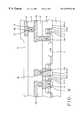
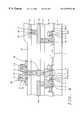
- FIGS. 1-9which schematically show, in cross-sectional style, the key fabrication stages used in the creation of a DRAM device, with a Capacitor Over Metal, (COM), STC structure, formed after the formation of metal interconnect structures.
- COMCapacitor Over Metal
- the transfer gate transistorused for this DRAM device, in this invention, will be an N channel device.
- the COM, stacked capacitor structure, described in this inventioncan also be applied to P channel, transfer gate transistor.
- a P type, semiconductor substrate 1with a ⁇ 100>, single crystalline orientation,is used.
- Field oxide (FOX), region 2is used for purposes of isolation.
- FOX region 2is formed via thermal oxidation, in an oxygen-steam ambient, at a temperature between about 850 to 1050° C., to a thickness between about 3000 to 5000 Angstroms.
- a patterned oxidation resistant mask of silicon nitride-silicon oxideis used to prevent FOX region 2 , from growing on areas of substrate, 1 , to be used for subsequent device regions.
- the oxidation resistant maskis removed via use of a hot phosphoric acid solution for the overlying, silicon nitride layer, and a buffered hydrofluoric acid solution for the underlying silicon oxide layer.
- a shallow trench isolation, (STI) processcan also be used to create the desired isolation regions provided by FOX regions 2 .
- a gate insulator layer 3of silicon oxide is thermally grown in an oxygen-steam ambient, at a temperature between about 750 to 1050° C., to a thickness between about 50 to 200 Angstroms.
- a first polysilicon layer 4is next deposited using low pressure chemical vapor deposition, (LPCVD), procedures, at a temperature between about 500 to 700° C., to a thickness between about 1000 to 4000 Angstroms.
- Polysilicon layer 4can either be grown intrinsically and doped via ion implantation of arsenic or phosphorous, at an energy between about 30 to 80 KeV, at a dose between about 1E113 to 1E16 atoms/cm 2 , or grown using in situ doping procedures, via the incorporation of either arsine or phosphine to the silane ambient.
- a silicon nitride layer 5is next deposited via LPCVD or plasma enhanced chemical vapor deposition, (PECVD), procedures, to a thickness between about 1000 to 3000 Angstroms.
- PECVDplasma enhanced chemical vapor deposition
- Conventional photolithographic and reactive ion etching, (RIE), procedures, using either CF 4 —O 2 —H 2 , C 2 F 6 , or CHF 3 , as an etchant for silicon nitride layer 5 , and using Cl 2 , or other chlorine based gases, as an etchant for polysilicon layer 4are used to create polycide gate structures comprised of silicon nitride layer 5 , and polysilicon layer 4 , shown schematically in FIG. 1 .
- Photoresist removalis accomplished via plasma oxygen ashing and careful wet cleans.
- a lightly doped source and drain region 6is next formed via ion implantation of phosphorous, at an energy between about 20 to 50 KeV, at a dose between about 1E13 to 1E14 atoms/cm 2 .
- a silicon nitrideis then deposited using either LPCVD or PECVD procedures, at a temperature between about 400 to 700° C., to a thickness between about 500 to 2000 Angstroms, followed by an anisotropic RIE procedure, using either CF 4 —O 2 H 2 , C 2 F 6 , or CHF 3 , as an etchant, creating silicon nitride insulator spacers 7 , on the sides of the polycide gate structures.
- a heavily doped source and drain region 8is then formed via ion implantation of arsenic, at an energy between about 30 to 80 KeV, at a dose between about 1E15 to 1E16 atoms/cm 2 .
- Heavily doped source and drain region 8is an optional.
- the DRAM structure in this inventioncan be formed using only lightly doped source and drain region 6 . The result of these procedures are schematically shown in FIG. 1 .
- a first insulator layer of silicon oxide 9is next deposited using LPCVD or PECVD procedures, at a temperature between about 200 to 600° C., to a thickness between about 3000 to 8000 Angstroms, followed by a planarization procedure, using a chemical mechanical polishing, (CMP), procedure, used to create a smooth top surface for insulator layer 9 .
- CMPchemical mechanical polishing
- Conductive polysilicon contact plugs 11are next formed.
- Polysilicon contact plugs 11are formed via deposition of a polysilicon layer, via LPCVD procedures, at a thickness between about 500 to 3000 Angstroms, doped during an in situ doping, deposition procedure, or grown intrinsically and doped via an arsenic, or a phosphorous, ion implantation procedure, followed by a patterning procedure, via anisotropic RIE procedures, using Cl 2 as an etchant, or via a CMP procedure.
- the conductive plugscan also be formed from tungsten, tungsten silicide, or other refractory metals, or metal suicides.
- a second insulator layer of silicon oxide 12is next deposited using either LPCVD or PECVD procedures, at a temperature between about 200 to 600° C., to a thickness between about 2500 to 7500 Angstroms.
- Insulator layer 12can also be a BPSG or PSG layer, obtained via addition of either PH 3 and B 2 H 6 , or just PH 3 , to a TEOS, (tetraethylorthosilicate), ambient.
- Photolithographic and RIE procedure, using CHF 3 as an etchant for second insulator layer 12are used to create shallow via holes 13 a , exposing the top surface of polysilicon contact plugs 11 .
- the RIE procedureis then extended to create deep via hole 13 b , in second insulator layer 12 , and in first insulator layer 9 , exposing a heavily doped region, in semiconductor substrate 1 .
- Thisis schematically shown in FIG. 3 .
- a deposition of a titanium—titanium nitride, (Ti—TiN), layer 14is next made, via R.F. sputtering, or via a CVD procedure, to a thickness between about 200 to 800 Angstroms for titanium, and between about 500 to 1500 Angstroms for titanium nitride.
- tungsten layer 15obtained via LPCVD or R.F. sputtering procedures, to a thickness between about 600 to 2500 Angstroms, completely filling shallow via holes 13 a , and deep via hole 13 b .
- Unwanted regions of Ti—TiN layer 14 , and tungsten layer 15are removed using either a CMP procedure, or an anisotropic RIE procedure, using Cl 2 as an etchant, creating the first level metal studs, comprised of tungsten layer 15 , and underlying Ti—TiN layer 14 , contacting polysilicon contact studs, in shallow via holes 13 a , and contacting a heavily doped source and drain region, in deep via hole 13 b , shown schematically in FIG. 3 .
- the first level metal structurescan also be formed from an LPCVD tungsten layer.
- a third insulator layer 17of silicon oxide is deposited using a PECVD procedures, at a temperature between about 200 to 600° C., to a thickness between about 3000 to 8000 Angstroms, followed by a CMP procedure, used to planarize the top surface of third insulator layer 17 .
- PECVD proceduresat a temperature between about 200 to 600° C., to a thickness between about 3000 to 8000 Angstroms, followed by a CMP procedure, used to planarize the top surface of third insulator layer 17 .
- Second level metal stud 20is formed via deposition of a TiN layer 19 , via an R.F. sputtering, or a CVD procedure, at a thickness between about 500 to 1500 Angstroms, and by a deposition of a tungsten layer 20 , using either LPCVD or R.F.
- a second level metal interconnect structure 40is next formed, and schematically shown in FIG. 6.
- a deposition of an aluminum based metallization layer, via R.F. sputtering,is followed by photolithographic and anisotropic RIE procedures, using Cl 2 as an etchant for the aluminum based metallization layer, creating second level metal interconnect structure 40 .
- a fourth insulator layer 41is deposited. Fourth insulator layer, schematically shown in FIG.
- the overlying silicon nitride layer, of composite fourth insulator layer 41is between about 500 to 1500 Angstroms in thickness.
- Via hole 42is next formed in fourth insulator layer 41 , and in third insulator 17 , via photolithographic and anisotropic RIE procedures, using either CF 4 —O 2 —H 2 , C 2 F 6 , or CHF 3 as an etchant for silicon nitride, while using CHF 3 as an etchant for silicon oxide, exposing the top surface of metal plug 16 b .
- a third level metal stud 50is formed in via hole 42 , and shown schematically in FIG. 7 .
- Third level metal stud 50is comprised of a TiN barrier layer, and a tungsten fill.
- the TiN barrier layeris deposited using R.F. sputtering, or CVD procedures, while the tungsten fill layer is also obtained via R.F. sputtering or LPCVD procedures. Unwanted regions of TiN and tungsten, overlaying the top surface of fourth insulator layer 41 , are removed using CMP procedures, creating third level metal stud 50 , in via hole 42 .
- a polysilicon layer 21 ais next deposited via an LPCVD procedure, to a thickness between about 250 to 2000 Angstroms. Polysilicon layer 21 a can be doped during an in situ doping deposition procedure, or grown intrinsically and doped via an arsenic or phosphorous ion implantation procedure. This is schematically shown in FIG. 7 .
- An insulator layeris next deposited using LPCVD or PECVD procedures, to a thickness between about 2000 to 12000 Angstroms, and then patterned via photolithographic and anisotropic RIE procedures, using CHF 3 procedures, to create insulator shape 22 , shown schematically in FIG. 8 .
- the thickness of the insulator layer, used for insulator shape 22will influence the amount of surface area for the subsequent stacked capacitor structure.
- Another polysilicon layeris next deposited, again via an LPCVD procedure, to a thickness between about 2000 to 3000 Angstroms.
- a selective, anisotropic RIE procedureusing Cl 2 as an etchant, is used to create polysilicon spacer 23 , on the sides of insulator shape 22 , while removing regions of polysilicon layer 21 a , not covered by insulator shape 22 , resulting in a lower electrode, or storage node structure, comprised of polysilicon spacers 23 , connected to a horizontal, polysilicon shape 21 b , lying on the smooth top surface of fourth insulator layer 41 , and with polysilicon shape 21 b , contacting third level metal stud 50 .
- the height of polysilicon spacers 23is the thickness of insulator shape 22 , between about 2000 to 12000 Angstroms. This is schematically shown in FIG. 8 .
- Dielectric layer 24can be an insulator layer possessing a high dielectric constant, such as Ta 2 O 5 , obtained via r.f sputtering, or CVD techniques, at an equivalent silicon dioxide thickness between about 20 to 40 Angstroms. Dielectric layer 24 , can also be ONO, (Oxidized—silicon Nitride—silicon Oxide).
- the ONO layeris formed by initially growing a silicon dioxide layer, between about an 10 to 50 Angstroms, followed by the deposition of a silicon nitride layer, between about 10 to 20 Angstroms. Subsequent thermal oxidation of the silicon nitride layer results in the formation of a silicon oxynitride layer on silicon oxide, at a silicon oxide equivalent thickness of between about 40 to 80 Angstroms.
- Dielectric layer 24can also be a barium strontium titanate, (BST), or a lead zirconate titanate, (PZT), layer. Finally another layer of polysilicon is deposited, via LPCVD procedures, at a temperature between about 500 to 700° C., to a thickness between about 1000 to 3000 Angstroms.
- Doping of this polysilicon layeris accomplished via either an in situ deposition procedure, via the addition of phosphine, to a silane ambient, or via an arsenic or phosphorous ion implantation procedure, applied to an intrinsic polysilicon layer.
- Photolithographic and anisotropic RIE procedures, using Cl 2 as an etchant,are next employed to create polysilicon upper electrode, or plate electrode 25 , shown schematically in FIG. 9 .
- Photoresistis again removed via plasma oxygen ashing and careful wet cleans, resulting in stacked capacitor structure 26 , laying on the smooth top surface of fourth insulator layer 41 , and contacting the source and drain region, in semiconductor substrate 1 , using third level metal stud 50 , in via hole 42 , second level metal stud, using metal plug 16 b , using first level metal stud in shallow via hole 13 a , and using a polysilicon contact plug 11 .
Landscapes
- Engineering & Computer Science (AREA)
- Manufacturing & Machinery (AREA)
- Semiconductor Memories (AREA)
Abstract
Description
(1) Field of the Invention
The present invention relates to a fabrication method used to create a stacked capacitor structure, for a DRAM device, in which the stacked capacitor structure is created after formation of DRAM interconnect metal structures.
(2) Description of the Prior Art
The objectives of the semiconductor industry are to continually improve device performance, while still attempting to decrease the manufacturing cost of specific semiconductor chips. These objectives have been in part realized by the ability of the semiconductor industry to produce chips with sub-micron features, or micro-miniaturization. Smaller features allow the reduction in performance degrading capacitances and resistances to be realized. In addition smaller features result in a smaller chip, however possessing the same level of integration obtained for semiconductor chips fabricated with larger features. This allows a greater number of the denser, smaller chips to be obtained from a specific size starting substrate, thus resulting in a lower manufacturing cost for an individual chip.
The use of smaller features, when used for the fabrication of dynamic random access memory, (DRAM), devices, in which the capacitor of the DRAM device is a stacked capacitor, (STC), structure, presents difficulties when attempting to increase STC capacitance. A DRAM cell is usually comprised of the STC structure, overlying a transfer gate transistor, and connected to the source of the transfer gate transistor. However the decreasing size of the transfer gate transistor, limits the dimensions of the STC structure. To increase the capacitance of the STC structure, comprised of two electrodes, separated by a dielectric layer, either the thickness of the dielectric layer has to be decreased, or the area of the capacitor has to be increased. The reduction in dielectric thickness is limited by increasing reliability and yield risks, encountered with ultra thin dielectric layers. In addition the area of the STC structure is limited by the area of the underlying transfer gate transistor dimensions. The advancement of the DRAM technology to densities of 64 million cells per chip, or greater, has resulted in a specific cell in which a smaller transfer gate transistor is being used, and thus limiting the amount of area the overlying STC structure can occupy, without interfering with neighboring cells.
Solutions to the shrinking design area, assigned to STC structures, have been addressed via novel semiconductor fabrication processes which result in an increase in surface area for only the lower, or storage electrode, of the STC structure, while maintaining the area original design area of the STC structure. One method for achieving this objective has been accomplished by creating lower electrodes with pillars, or protruding shapes of polysilicon, thus resulting in a greater electrode surface area then would have been achieved with conventional flat surfaces. Kim, in U.S. Pat. No. 5,447,882, describes such an STC structure, comprised of a lower electrode, formed by creating protruding polysilicon features, via patterning of a polysilicon layer, however the topography created with these novel STC configurations present difficulties for subsequent formation of overlying interconnect metal structures. For example thick insulator layers are needed for adequate coverage of the STC structure, which presents additional problems when opening vias in the thick insulator layer, and then attempting to fill the high aspect ratio via holes with metal. Thus the capacitor under bit line, (CUM), structure, can result in yield and reliability problems resulting from poor metal coverage, in high aspect ratio holes.
This invention will describe a process, and a structure, in which the capacitor structure is constructed after formation of the metal interconnect levels. After passivation of underlying metal interconnect structures with insulator layers, and planarization of the insulator layer, the stacked capacitor structure is formed over the passivated metal structures, (Capacitor Over Metal—COM), thus avoiding formation of metal interconnects over severe topologies created from an underlying STC structure.
It is an object of this invention to create a DRAM device, with an STC structure, in which the surface area of the lower electrode, of the STC structure is increased, without creating the high aspect ratios of metal via holes encountered using conventional capacitor under metal, (CUM), stacked capacitor structures.
It is another object of this invention to form the STC structure after the formation of metal interconnect structures, on a planarized, smooth top surface of an insulator layer, used on the underlying metal interconnect structures.
In accordance with the present invention a method for fabricating a DRAM device, with an STC structure that is formed after the formation of metal interconnect structures, has been developed. A transfer gate transistor comprised of: a thin gate insulator; a polysilicon gate structure; lightly doped source and drain regions; insulator spacers on the sidewalls of the polysilicon gate structure; and/or heavily doped source and drain regions; is formed on a semiconductor substrate. Polysilicon plugs are formed in a first insulator layer, contacting a source and drain region between polysilicon gate structures. A second insulator layer is deposited, followed by the formation of shallow, first level metal studs, located in shallow via holes that had been created in the second insulator layer, with the shallow, first level metal studs contacting the polysilicon plugs. A deep via hole, however shallower than via holes used in conventional CUM DRAM structures, is also formed in the second, and in the first insulator layers, allowing a deep, first level metal stud to be created, with the deep, first level metal stud contacting a region of the semiconductor substrate, exposed in the deep via hole. Metal structures are next formed, and used for: a bit line structure contacting a first, shallow, first level metal stud; a first level metal interconnect structure, contacting the deep, first level metal stud; and for a metal plug, contacting a second, shallow, first metal stud. A third insulator layer is deposited, and planarized, followed by the opening of a via hole, exposing the top surface of the first level metal interconnect structure. A second level metal stud is next formed in the via hole in the third insulator layer. A second level interconnect structure is next formed, contacting a second level metal stud, which in turn overlays and contacts a first level metal interconnect structure. A fourth insulator layer is deposited followed by creation of a third level metal stud. A stacked capacitor structure is finally formed on the fourth insulator layer, contacting the third level metal stud, in a region in which the third level metal stud overlays the metal plug, allowing contact between the STC structure and a source and drain region, of the transfer gate transistor. The capacitor structure, and process used for formation, described in this invention is shown overlaying only two levels of metal interconnect structures, however this invention can be applied to overlay as many metal interconnect levels as desired.
The object and other advantages of this invention are best explained in the preferred embodiment with reference to the attached drawings that include:
FIGS. 1-9, which schematically show, in cross-sectional style, the key fabrication stages used in the creation of a DRAM device, with a Capacitor Over Metal, (COM), STC structure, formed after the formation of metal interconnect structures.
The method of forming a DRAM device, featuring a COM, stacked capacitor structure, will now be described in detail. The transfer gate transistor, used for this DRAM device, in this invention, will be an N channel device. However the COM, stacked capacitor structure, described in this invention, can also be applied to P channel, transfer gate transistor.
Referring to FIG. 1, a P type, semiconductor substrate1, with a <100>, single crystalline orientation,is used. Field oxide (FOX),region 2, is used for purposes of isolation. Briefly the FOXregion 2, is formed via thermal oxidation, in an oxygen-steam ambient, at a temperature between about 850 to 1050° C., to a thickness between about 3000 to 5000 Angstroms. A patterned oxidation resistant mask of silicon nitride-silicon oxide is used to prevent FOXregion 2, from growing on areas of substrate,1, to be used for subsequent device regions. After the growth of the FOXregions 2, the oxidation resistant mask is removed via use of a hot phosphoric acid solution for the overlying, silicon nitride layer, and a buffered hydrofluoric acid solution for the underlying silicon oxide layer. A shallow trench isolation, (STI), process can also be used to create the desired isolation regions provided by FOXregions 2. After a series of wet cleans, agate insulator layer 3, of silicon oxide is thermally grown in an oxygen-steam ambient, at a temperature between about 750 to 1050° C., to a thickness between about 50 to 200 Angstroms. Afirst polysilicon layer 4, is next deposited using low pressure chemical vapor deposition, (LPCVD), procedures, at a temperature between about 500 to 700° C., to a thickness between about 1000 to 4000 Angstroms.Polysilicon layer 4, can either be grown intrinsically and doped via ion implantation of arsenic or phosphorous, at an energy between about 30 to 80 KeV, at a dose between about 1E113 to 1E16 atoms/cm2, or grown using in situ doping procedures, via the incorporation of either arsine or phosphine to the silane ambient. Asilicon nitride layer 5, is next deposited via LPCVD or plasma enhanced chemical vapor deposition, (PECVD), procedures, to a thickness between about 1000 to 3000 Angstroms. Conventional photolithographic and reactive ion etching, (RIE), procedures, using either CF4—O2—H2, C2F6, or CHF3, as an etchant forsilicon nitride layer 5, and using Cl2, or other chlorine based gases, as an etchant forpolysilicon layer 4, are used to create polycide gate structures comprised ofsilicon nitride layer 5, andpolysilicon layer 4, shown schematically in FIG.1. Photoresist removal is accomplished via plasma oxygen ashing and careful wet cleans.
A lightly doped source anddrain region 6, is next formed via ion implantation of phosphorous, at an energy between about 20 to 50 KeV, at a dose between about 1E13 to 1E14 atoms/cm2. A silicon nitride is then deposited using either LPCVD or PECVD procedures, at a temperature between about 400 to 700° C., to a thickness between about 500 to 2000 Angstroms, followed by an anisotropic RIE procedure, using either CF4—O2H2, C2F6, or CHF3, as an etchant, creating siliconnitride insulator spacers 7, on the sides of the polycide gate structures. A heavily doped source anddrain region 8, is then formed via ion implantation of arsenic, at an energy between about 30 to 80 KeV, at a dose between about 1E15 to 1E16 atoms/cm2. Heavily doped source anddrain region 8, is an optional. The DRAM structure in this invention can be formed using only lightly doped source anddrain region 6. The result of these procedures are schematically shown in FIG.1.
A first insulator layer ofsilicon oxide 9, is next deposited using LPCVD or PECVD procedures, at a temperature between about 200 to 600° C., to a thickness between about 3000 to 8000 Angstroms, followed by a planarization procedure, using a chemical mechanical polishing, (CMP), procedure, used to create a smooth top surface forinsulator layer 9. Conventional photolithographic and RIE procedures, using CHF3as an etchant, are used to open self-aligned contact, (SAC), holes10, insilicon oxide layer 9, exposing the top surface of heavily doped source and drainregion 8, between the silicon nitride encapsulated, polycide gate structures. Photoresist removal is performed via use of plasma oxygen ashing and careful wet cleans. Conductive polysilicon contact plugs11, schematically shown in FIG. 2, are next formed. Polysilicon contact plugs11, are formed via deposition of a polysilicon layer, via LPCVD procedures, at a thickness between about 500 to 3000 Angstroms, doped during an in situ doping, deposition procedure, or grown intrinsically and doped via an arsenic, or a phosphorous, ion implantation procedure, followed by a patterning procedure, via anisotropic RIE procedures, using Cl2as an etchant, or via a CMP procedure. The conductive plugs can also be formed from tungsten, tungsten silicide, or other refractory metals, or metal suicides.
A second insulator layer ofsilicon oxide 12, is next deposited using either LPCVD or PECVD procedures, at a temperature between about 200 to 600° C., to a thickness between about 2500 to 7500 Angstroms.Insulator layer 12, can also be a BPSG or PSG layer, obtained via addition of either PH3and B2H6, or just PH3, to a TEOS, (tetraethylorthosilicate), ambient. Photolithographic and RIE procedure, using CHF3as an etchant forsecond insulator layer 12, are used to create shallow viaholes 13a, exposing the top surface of polysilicon contact plugs11. The RIE procedure is then extended to create deep viahole 13b, insecond insulator layer 12, and infirst insulator layer 9, exposing a heavily doped region, in semiconductor substrate1. This is schematically shown in FIG.3. After removal of the photoresist shape used as a mask for via hole formation, a deposition of a titanium—titanium nitride, (Ti—TiN),layer 14, is next made, via R.F. sputtering, or via a CVD procedure, to a thickness between about 200 to 800 Angstroms for titanium, and between about 500 to 1500 Angstroms for titanium nitride. This is followed by the deposition of atungsten layer 15, obtained via LPCVD or R.F. sputtering procedures, to a thickness between about 600 to 2500 Angstroms, completely filling shallow viaholes 13a, and deep viahole 13b. Unwanted regions of Ti—TiN layer 14, andtungsten layer 15, are removed using either a CMP procedure, or an anisotropic RIE procedure, using Cl2as an etchant, creating the first level metal studs, comprised oftungsten layer 15, and underlying Ti—TiN layer 14, contacting polysilicon contact studs, in shallow viaholes 13a, and contacting a heavily doped source and drain region, in deep viahole 13b, shown schematically in FIG.3.
A metal layer of aluminum, containing between about 0 to 2% copper, is deposited using R.F. sputtering procedures, to a thickness between about 1500 to 6000 Angstroms. Photolithographic and RIE procedures, using Cl2as an etchant, are then employed to create first level metal structures:16a, to be used as a bit line structure, contacting one of the firstlevel metal studs 13a;16b, to be used as metal plug, contacting the other firstlevel metal stud 13a; and16c, to be used as a first level metal interconnect structure, contacting firstlevel metal stud 13b. The first level metal structures can also be formed from an LPCVD tungsten layer. After removal of the masking photoresist layer, via plasma oxygen ashing and careful wet cleans, athird insulator layer 17, of silicon oxide is deposited using a PECVD procedures, at a temperature between about 200 to 600° C., to a thickness between about 3000 to 8000 Angstroms, followed by a CMP procedure, used to planarize the top surface ofthird insulator layer 17. The result of these procedures are schematically shown in FIG.4.
Photolithographic and RIE procedures, using CHF3as an etchant, are used to create viahole 18b, inthird insulator layer 17, with viahole 18b, exposing the top surface of first levelmetal interconnect structure 16c. After removal of photoresist via plasma oxygen ashing and careful wet cleans, secondlevel metal stud 20, are formed in viahole 18b, shown schematically in FIG.5. Secondlevel metal stud 20, is formed via deposition of aTiN layer 19, via an R.F. sputtering, or a CVD procedure, at a thickness between about 500 to 1500 Angstroms, and by a deposition of atungsten layer 20, using either LPCVD or R.F. sputtering procedures, to a thickness between about 3000 to 8000 Angstroms. Unwanted regions of these layers are removed using either CMP, or a selective, anisotropic RIE procedure, using Cl2as an etchant, resulting in the secondlevel metal stud 20, residing viahole 18b.
A second levelmetal interconnect structure 40, is next formed, and schematically shown in FIG. 6. A deposition of an aluminum based metallization layer, via R.F. sputtering, is followed by photolithographic and anisotropic RIE procedures, using Cl2as an etchant for the aluminum based metallization layer, creating second levelmetal interconnect structure 40. After removal of the photoresist shape, used as a mask for patterning of second levelmetal interconnect structure 40, via plasma oxygen ashing and careful wet cleans, afourth insulator layer 41, is deposited. Fourth insulator layer, schematically shown in FIG. 6, is a composite layer comprised of a silicon oxide layer, capped with an overlying silicon nitride layer, deposited using PECVD procedures. The overlying silicon nitride layer, of compositefourth insulator layer 41, is between about 500 to 1500 Angstroms in thickness.
Viahole 42, is next formed infourth insulator layer 41, and inthird insulator 17, via photolithographic and anisotropic RIE procedures, using either CF4—O2—H2, C2F6, or CHF3as an etchant for silicon nitride, while using CHF3as an etchant for silicon oxide, exposing the top surface ofmetal plug 16b. After removal of the masking photoresist layer, via plasma oxygen ashing and careful wet cleans, a thirdlevel metal stud 50, is formed in viahole 42, and shown schematically in FIG.7. Thirdlevel metal stud 50, is comprised of a TiN barrier layer, and a tungsten fill. The TiN barrier layer is deposited using R.F. sputtering, or CVD procedures, while the tungsten fill layer is also obtained via R.F. sputtering or LPCVD procedures. Unwanted regions of TiN and tungsten, overlaying the top surface offourth insulator layer 41, are removed using CMP procedures, creating thirdlevel metal stud 50, in viahole 42. Apolysilicon layer 21a, is next deposited via an LPCVD procedure, to a thickness between about 250 to 2000 Angstroms.Polysilicon layer 21acan be doped during an in situ doping deposition procedure, or grown intrinsically and doped via an arsenic or phosphorous ion implantation procedure. This is schematically shown in FIG.7.
An insulator layer is next deposited using LPCVD or PECVD procedures, to a thickness between about 2000 to 12000 Angstroms, and then patterned via photolithographic and anisotropic RIE procedures, using CHF3procedures, to createinsulator shape 22, shown schematically in FIG.8. The thickness of the insulator layer, used forinsulator shape 22, will influence the amount of surface area for the subsequent stacked capacitor structure. Another polysilicon layer is next deposited, again via an LPCVD procedure, to a thickness between about 2000 to 3000 Angstroms. A selective, anisotropic RIE procedure, using Cl2as an etchant, is used to createpolysilicon spacer 23, on the sides ofinsulator shape 22, while removing regions ofpolysilicon layer 21a, not covered byinsulator shape 22, resulting in a lower electrode, or storage node structure, comprised ofpolysilicon spacers 23, connected to a horizontal,polysilicon shape 21b, lying on the smooth top surface offourth insulator layer 41, and withpolysilicon shape 21b, contacting thirdlevel metal stud 50. The height ofpolysilicon spacers 23, is the thickness ofinsulator shape 22, between about 2000 to 12000 Angstroms. This is schematically shown in FIG.8.
The completion of the stacked capacitor structure is schematically shown in FIG.9.First insulator shape 22, is removed via HF vapors, or a HF wet solution. Next adielectric layer 24, is formed, overlying the storage node structure.Dielectric layer 24, can be an insulator layer possessing a high dielectric constant, such as Ta2O5, obtained via r.f sputtering, or CVD techniques, at an equivalent silicon dioxide thickness between about 20 to 40 Angstroms.Dielectric layer 24, can also be ONO, (Oxidized—silicon Nitride—silicon Oxide). The ONO layer is formed by initially growing a silicon dioxide layer, between about an 10 to 50 Angstroms, followed by the deposition of a silicon nitride layer, between about 10 to 20 Angstroms. Subsequent thermal oxidation of the silicon nitride layer results in the formation of a silicon oxynitride layer on silicon oxide, at a silicon oxide equivalent thickness of between about 40 to 80 Angstroms.Dielectric layer 24, can also be a barium strontium titanate, (BST), or a lead zirconate titanate, (PZT), layer. Finally another layer of polysilicon is deposited, via LPCVD procedures, at a temperature between about 500 to 700° C., to a thickness between about 1000 to 3000 Angstroms. Doping of this polysilicon layer is accomplished via either an in situ deposition procedure, via the addition of phosphine, to a silane ambient, or via an arsenic or phosphorous ion implantation procedure, applied to an intrinsic polysilicon layer. Photolithographic and anisotropic RIE procedures, using Cl2as an etchant, are next employed to create polysilicon upper electrode, orplate electrode 25, shown schematically in FIG.9. Photoresist is again removed via plasma oxygen ashing and careful wet cleans, resulting in stackedcapacitor structure 26, laying on the smooth top surface offourth insulator layer 41, and contacting the source and drain region, in semiconductor substrate1, using thirdlevel metal stud 50, in viahole 42, second level metal stud, usingmetal plug 16b, using first level metal stud in shallow viahole 13a, and using apolysilicon contact plug 11.
While this invention has been particularly shown and described with reference to the preferred embodiments thereof, it will be understood by those skilled in the art that various changes in form and details may be made without departing from the spirit and scope of this invention.
Claims (29)
1. A method of fabricating a DRAM device, on a semiconductor substrate, with a Capacitor Over Metal, (COM), stacked capacitor structure, comprising the steps of:
providing a first transfer gate transistor, comprised of polysilicon gate structures, on a gate insulator layer, with a first source and drain region in said semiconductor substrate, in an area not covered by said polysilicon gate structures;
providing a second source and drain region in said semiconductor substrate, for a second transfer gate transistor;
forming contact plugs, in contact holes in a first insulator layer, with the contact plugs placed between said polysilicon gate structures of said first transfer gate transistor, and with said contact plugs, contacting said first source and drain region, of said first transfer gate transistor;
forming short, first level metal studs, in shallow via holes, created in a second insulator layer, with said short, first level metal studs contacting the top surface of said contact plugs;
forming a tall, first level metal stud, in a deep via hole, created in said second insulator layer, and in said first insulator layer, with said tall, first level metal stud contacting said second source and drain region, of said second transfer gate transistor;
forming a metal bit line structure, contacting the top surface of a first, short, first level metal stud;
forming a metal plug contacting the top surface of a second, short first level metal stud;
forming a first level metal interconnect structure, contacting the top surface of said tall, first level metal stud;
forming a second level metal stud in a via hole created in a third insulator layer, with said second level metal stud contacting the top surface of said first level interconnect structure;
forming a third level metal stud in a via hole created in a fourth insulator layer, and in said third insulator layer, with said third level metal stud contacting the top surface of said metal plug; and
forming said COM, stacked capacitor structure, on the top surface of said fourth insulator layer, and with said COM, stacked capacitor structure contacting the top surface of said third level metal stud.
2. The method ofclaim 1 , wherein said gate insulator layer is silicon dioxide, thermally grown in an oxygen steam ambient, at a temperature between about 850 to 1050° C., to a thickness between about 50 to 200 Angstroms.
3. The method ofclaim 1 , wherein said first insulator layer is silicon oxide, deposited using LPCVD or PECVD procedures, to a thickness between about 3000 to 8000 Angstroms, with the top surface of said first insulator layer planarized using a CMP procedure.
4. The method ofclaim 1 , wherein said contact holes, formed in said first insulator layer, are formed between, and self-aligned to, said polysilicon gate structures of said first transfer gate transistor, and with said contact holes formed via a RIE procedure, using CHF3as an etchant.
5. The method ofclaim 1 , wherein said polysilicon contact plugs are formed via deposition of a polysilicon layer, using an LPCVD procedure, to a thickness between about 500 to 3000 Angstroms, and doped during an in situ deposition procedure, or doped via an arsenic or phosphorous ion implantation procedure, and patterned by removal of unwanted regions of the polysilicon layer, on the top surface of said first insulator layer, via an anisotropic RIE procedure, using Cl2as an etchant, or by removal of unwanted regions of polysilicon using a CMP procedure.
6. The method ofclaim 1 , wherein said second insulator layer is silicon oxide, deposited using either LPCVD or PECVD procedures, at a temperature between about 200 to 600° C., to a thickness between about 2500 to 7500 Angstroms.
7. The method ofclaim 1 , wherein said short, first level metal studs, in said shallow via holes, and said tall, first level metal stud, in said deep via hole, are comprised of: an underlying titanium—titanium nitride layer, deposited using R.F. sputtering, to a titanium thickness between about 200 to 800 Angstroms, and to a titanium nitride thickness between about 500 to 1500 Angstroms; and comprised of a tungsten layer, deposited using R.F. sputtering or LPCVD procedures, to a thickness between about 600 to 2500 Angstroms.
8. The method ofclaim 1 , wherein said metal bit line structure, said metal plug, and said first level metal interconnect structure, are comprised of an aluminum layer, containing between about 0 to 2% copper, at a thickness between about 1500 to 6000 Angstroms.
9. The method ofclaim 1 , wherein said third insulator layer is silicon nitride, deposited using a PECVD procedure, at a temperature between about 200 to 600° C., to a thickness between about 3000 to 8000 Angstroms, and with the top surface of said third insulator layer planarized using a CMP procedure.
10. The method ofclaim 1 , wherein said second level metal studs are comprised of an underlying titanium nitride layer, obtained using an R.F. sputtering procedure, to a thickness between about 500 to 1500 Angstroms, and an overlying tungsten layer, obtained using an R.F. sputtering procedure, or by using a LPCVD procedure, to a thickness between about 3000 to 8000 Angstroms.
11. The method ofclaim 1 , wherein said fourth insulator layer is a composite insulator layer, comprised of: an overlying silicon nitride layer, deposited via PECVD procedures to a thickness between about 500 to 1500 Angstroms; and comprised of an underlying silicon oxide layer.
12. The method ofclaim 1 , wherein said third level metal stud is comprised of an underlying titanium nitride layer, and a tungsten layer, deposited using R.F. sputtering or CVD procedures.
13. The method ofclaim 1 , wherein the storage node structure, of said COM, stacked capacitor structure, is comprised of an N type doped, horizontal polysilicon shape, at a thickness between about 250 to 2000 Angstroms, and polysilicon spacers, connected to said horizontal polysilicon shape, at a thickness between about 250 to 3000 Angstroms, with said polysilicon spacers at a height between about 2000 to 12000 Angstroms.
14. The method ofclaim 1 , wherein said dielectric layer is ONO, at an equivalent silicon dioxide thickness between about 40 to 80 Angstroms, created by an initial thermal oxidation to form a silicon oxide layer, between about 10 to 50 Angstroms, followed by a deposition of silicon nitride, to a thickness between about 10 to 20 Angstroms, and thermal oxidation of said silicon nitride layer, creating a silicon oxynitride layer, on the underlying, said silicon oxide layer.
15. The method ofclaim 1 , wherein said dielectric layer is Ta2O5, obtained via r.f. sputtering techniques, to an equivalent silicon dioxide thickness between about 20 to 40 Angstroms.
16. A method of fabricating a DRAM device, using a stacked capacitor structure, (STC), on a semiconductor substrate, created after the formation of underlying metal structures, and with the Capacitor Over Metal, (COM), stacked capacitor structure, formed on a insulator layer, comprising the steps of:
providing a first transfer gate transistor, on said semiconductor substrate, comprised of polysilicon gate structures on a silicon dioxide gate insulator layer, and with a first source and drain region, in said semiconductor substrate, between said polysilicon gate structures;
providing a second source and drain region in said semiconductor substrate, for a second transfer gate transistor;
depositing a first insulator layer;
planarizing said first insulator layer;
forming self-aligned contact openings, in said first insulator layer, to expose said first source and drain region;
depositing a first polysilicon layer, completely filling said self-aligned contact holes;
removing said first polysilicon layer from the top surface of said first insulator layer, resulting in the formation of polysilicon contact plugs, in said self-aligned contact holes;
depositing a second insulator layer;
opening shallow via holes in said second insulator layer, exposing the top surface of said polysilicon contact plugs;
opening a deep via hole in said second insulator layer, and in said first insulator layer, exposing the top surface of said second source and drain region;
depositing a first titanium nitride layer;
depositing a first tungsten layer, completely filling said shallow via holes, and completely filling said deep via hole;
removing said first tungsten layer, and said first titanium nitride layer, from the top surface of said second insulator layer, resulting in short, first level tungsten studs, in said shallow via holes, and resulting in a tall, first level tungsten stud, in said deep via hole;
depositing an aluminum based layer;
patterning of said aluminum based layer to form an aluminum based, bit line structure, contacting the top surface of a first, short, first level tungsten stud;
patterning of said aluminum based layer to form an aluminum based, metal plug, contacting the top surface of a second, short, first level tungsten stud;
patterning of said aluminum based layer to form an aluminum based, first level interconnect structure, contacting the top surface of said tall, first level tungsten stud;
depositing a third insulator layer;
planarizing said third insulator layer;
opening a via hole in said third insulator layer, exposing the top surface of said aluminum based, first level interconnect structure;
depositing a second titanium nitride layer;
depositing a second tungsten layer, completely filling via hole in said third insulator layer;
removing said second tungsten layer, and said second titanium nitride layer, from the top surface of said third insulator layer, creating a second level tungsten stud, in the via hole in said third insulator layer, contacting the top surface of said aluminum based, first level interconnect structure;
depositing a fourth insulator layer;
opening a via hole in said fourth insulator layer, and in said third insulator layer, exposing the top surface of said aluminum based metal plug;
depositing a third titanium nitride layer;
depositing a third tungsten layer;
removing said third tungsten layer, and said third titanium nitride layer, from the top surface of said fourth insulator layer, creating a third level tungsten stud, in the via hole in said fourth insulator layer, and in said third insulator layer, contacting the top. surface of said aluminum based metal plug;
depositing a second polysilicon layer;
depositing a fifth insulator layer;
patterning of said fifth insulator layer, to create an insulator shape on said second polysilicon layer;
depositing a third polysilicon layer;
anisotropic etching of said third polysilicon layer, to create polysilicon spacers on the sides of said insulator shape;
removing said second polysilicon layer, from the top surface of said fourth insulator layer, in a region in which said second polysilicon layer is not covered by said insulator shape, creating a horizontal polysilicon shape, underlying said insulator shape;
removing said insulator shape from the top surface of said horizontal polysilicon shape, creating a polysilicon storage node structure, for said COM, stacked capacitor structure, comprised of vertical, said polysilicon spacers, connected to said horizontal polysilicon shape;
forming a dielectric layer on said storage node structure, of said COM, stacked capacitor structure;
depositing a fourth polysilicon layer on said dielectric layer; and
patterning of said fourth polysilicon layer to form the plate electrode, of said COM, stacked capacitor structure.
17. The method ofclaim 16 , wherein said first insulator layer is silicon oxide obtained via LPCVD procedures, to a thickness between about 3000 to 8000 Angstroms.
18. The method ofclaim 16 , wherein said first polysilicon layer, used for said polysilicon contact plugs, is deposited using LPCVD procedures, to a thickness between about 500 to 3000 Angstroms, and doped in situ during deposition, or deposited intrinsically and doped via an arsenic or phosphorous ion implantation procedure.
19. The method ofclaim 16 , wherein said second insulator layer is silicon oxide, deposited using LPCVD or PECVD procedures, to a thickness between about 2500 to 7500 Angstroms.
20. The method ofclaim 16 , wherein said first titanium nitride layer is deposited using R.F. sputtering, to a thickness between about 500 to 1500 Angstroms.
21. The method ofclaim 16 , wherein said first tungsten layer is deposited using LPCVD procedures, or R.F sputtering procedures, to a thickness between about 600 to 2500 Angstroms.
22. The method ofclaim 16 , wherein said aluminum based layer, contains between about 0 to 2% copper, and is deposited using R.F. sputtering, to a thickness between about 1500 to 6000 Angstroms.
23. The method ofclaim 16 , wherein said third insulator layer is silicon oxide, deposited using PECVD procedures, to a thickness between about 3000 to 8000 Angstroms, and planarized using a CMP procedure.
24. The method ofclaim 16 , wherein said second titanium nitride layer is deposited using R.F. sputtering, to a thickness between about 500 to 1500 Angstroms.
25. The method ofclaim 16 , wherein said second tungsten layer is deposited using an LPCVD procedure, or R.F. sputtering, to a thickness between about 3000 to 8000 Angstroms.
26. The method ofclaim 16 , wherein said second polysilicon layer is deposited using LPCVD procedures, to a thickness between about 250 to 2000 Angstroms, and doped during an in situ deposition procedure, or via an arsenic or phosphorous ion implantation procedure.
27. The method ofclaim 16 , wherein said third polysilicon layer is deposited using LPCVD procedures, to a thickness between about 250 to 3000 Angstroms.
28. The method ofclaim 16 , wherein said dielectric layer is ONO, with an equivalent silicon oxide thickness between about 40 to 80 Angstroms, created by growing a thin silicon oxide layer on said storage node electrode, at a thickness between about 10 to 50 Angstroms, depositing between about 10 to 20 Angstroms of a silicon nitride layer, and oxidizing said silicon nitride layer to from a silicon oxynitride layer on said thin silicon oxide layer.
29. The method ofclaim 16 , wherein said thin dielectric layer is Ta2O5, deposited using r.f. sputtering procedures, to an equivalent silicon dioxide thickness between about 20 to 40 Angstroms.
Priority Applications (1)
| Application Number | Priority Date | Filing Date | Title |
|---|---|---|---|
| US09/033,102US6479341B1 (en) | 1998-03-02 | 1998-03-02 | Capacitor over metal DRAM structure |
Applications Claiming Priority (1)
| Application Number | Priority Date | Filing Date | Title |
|---|---|---|---|
| US09/033,102US6479341B1 (en) | 1998-03-02 | 1998-03-02 | Capacitor over metal DRAM structure |
Publications (1)
| Publication Number | Publication Date |
|---|---|
| US6479341B1true US6479341B1 (en) | 2002-11-12 |
Family
ID=21868572
Family Applications (1)
| Application Number | Title | Priority Date | Filing Date |
|---|---|---|---|
| US09/033,102Expired - LifetimeUS6479341B1 (en) | 1998-03-02 | 1998-03-02 | Capacitor over metal DRAM structure |
Country Status (1)
| Country | Link |
|---|---|
| US (1) | US6479341B1 (en) |
Cited By (34)
| Publication number | Priority date | Publication date | Assignee | Title |
|---|---|---|---|---|
| US20030003733A1 (en)* | 1997-09-08 | 2003-01-02 | Naofumi Ohashi | Semiconductor integrated circuit device and fabrication process thereof |
| US20040029404A1 (en)* | 1998-12-21 | 2004-02-12 | Megic Corporation | High performance system-on-chip passive device using post passivation process |
| US20040110377A1 (en)* | 2002-11-22 | 2004-06-10 | Cho Yong-Joon | Method of forming a contact in a semiconductor device |
| US20040125538A1 (en)* | 1999-01-25 | 2004-07-01 | Carstensen Robert K. | Method for improved processing and etchback of a container capacitor |
| US20040129995A1 (en)* | 2003-01-02 | 2004-07-08 | Yee-Chia Yeo | Semiconductor chip with gate dielectrics for high-performance and low-leakage applications |
| US20040152256A1 (en)* | 2003-01-08 | 2004-08-05 | Renesas Technology Corp. | Semiconductor device manufacturing method |
| US20040157388A1 (en)* | 2003-01-28 | 2004-08-12 | Seo-Min Kim | Semiconductor memory device and method for fabricating the same |
| US20050035345A1 (en)* | 2003-08-11 | 2005-02-17 | Chun-Chieh Lin | Semiconductor device with high-k gate dielectric |
| US20050095857A1 (en)* | 2002-06-27 | 2005-05-05 | Chung Eun-Ae | Methods of forming contact plugs including polysilicon doped with an impurity having a lesser diffusion coefficient than phosphorus and related structures |
| US20050250307A1 (en)* | 2004-05-04 | 2005-11-10 | Jin-Taek Park | Interconnection structures for semicondcutor devices and methods of forming the same |
| US20050258512A1 (en)* | 2004-05-21 | 2005-11-24 | Taiwan Semiconductor Manufacturing Co., Ltd. | Topographically elevated microelectronic capacitor structure |
| US20060022256A1 (en)* | 2004-07-29 | 2006-02-02 | Doo-Young Lee | Semiconductor device and method of manufacturing the same |
| US7005388B1 (en)* | 2003-12-04 | 2006-02-28 | National Semiconductor Corporation | Method of forming through-the-wafer metal interconnect structures |
| US20060289920A1 (en)* | 2005-06-22 | 2006-12-28 | I-Lu Wu | Composite gate structure in an integrated circuit |
| US20070032015A1 (en)* | 2005-07-29 | 2007-02-08 | Fujitsu Limited | Semiconductor device and manufacturing method of the same |
| US20070037400A1 (en)* | 2005-08-11 | 2007-02-15 | Hwang Dong-Won | Composition and methods removing polysilicon |
| US20070093050A1 (en)* | 2004-06-25 | 2007-04-26 | Samsung Electronics Co., Ltd. | Interconnection structures for semiconductor devices and methods of forming the same |
| US20070096192A1 (en)* | 2005-10-28 | 2007-05-03 | Dongbu Electronics Co., Ltd. | Capacitor of semiconductor device and method of fabricating the same |
| US20080035974A1 (en)* | 1998-12-21 | 2008-02-14 | Megica Corporation | High performance system-on-chip using post passivation process |
| US20080064163A1 (en)* | 2006-09-13 | 2008-03-13 | International Business Machines Corporation | Method and structure for integrating mim capacitors within dual damascene processing techniques |
| US7482278B1 (en)* | 1999-02-11 | 2009-01-27 | Taiwan Semiconductor Manufacturing Co., Ltd. | Key-hole free process for high aspect ratio gap filling with reentrant spacer |
| US20090273881A1 (en)* | 2007-02-13 | 2009-11-05 | Semiconductor Manufacturing International (Shanghai) Corporation | Metal-Insulator-Metal Capacitor |
| US20100148228A1 (en)* | 2008-12-11 | 2010-06-17 | Hynix Semiconductor Inc. | Semiconductor and manufacturing method of the same |
| US7960269B2 (en) | 2005-07-22 | 2011-06-14 | Megica Corporation | Method for forming a double embossing structure |
| US7973629B2 (en) | 2001-09-04 | 2011-07-05 | Megica Corporation | Method for making high-performance RF integrated circuits |
| US8008775B2 (en) | 2004-09-09 | 2011-08-30 | Megica Corporation | Post passivation interconnection structures |
| US8018060B2 (en) | 2004-09-09 | 2011-09-13 | Megica Corporation | Post passivation interconnection process and structures |
| US8178435B2 (en) | 1998-12-21 | 2012-05-15 | Megica Corporation | High performance system-on-chip inductor using post passivation process |
| US8384189B2 (en) | 2005-03-29 | 2013-02-26 | Megica Corporation | High performance system-on-chip using post passivation process |
| US8421158B2 (en) | 1998-12-21 | 2013-04-16 | Megica Corporation | Chip structure with a passive device and method for forming the same |
| US20140145345A1 (en)* | 2012-11-27 | 2014-05-29 | Infineon Technologies Ag | Method of forming a semiconductor structure, and a semiconductor structure |
| US20160035668A1 (en)* | 2009-11-04 | 2016-02-04 | International Business Machines Corporation | Automated short lenght wire shape strapping and methods of fabricating the same |
| US10622073B2 (en)* | 2018-05-11 | 2020-04-14 | Texas Instruments Incorporated | Integrated circuit including vertical capacitors |
| US20240021475A1 (en)* | 2022-07-12 | 2024-01-18 | Vanguard International Semiconductor Corporation | Semiconductor structure and methods for manufacturing the same |
Citations (8)
| Publication number | Priority date | Publication date | Assignee | Title |
|---|---|---|---|---|
| US5447882A (en) | 1993-12-01 | 1995-09-05 | Hyundai Electronics Industries Co., Ltd. | Method for fabricating capacitor of semiconductor memory device |
| US5620917A (en) | 1992-11-27 | 1997-04-15 | Samsung Electronics Co., Ltd. | Method of manufacturing a semiconductor memory device having a capacitor |
| US5622883A (en) | 1995-05-31 | 1997-04-22 | Samsung Electronics Co., Ltd. | Method for manufacturing semiconductor memory device having landing pad |
| US5716881A (en)* | 1996-03-28 | 1998-02-10 | Taiwan Semiconductor Manufacturing Company, Ltd. | Process to fabricate stacked capacitor DRAM and low power thin film transistor SRAM devices on a single semiconductor chip |
| US5780339A (en)* | 1997-05-02 | 1998-07-14 | Vanguard International Semiconductor Corporation | Method for fabricating a semiconductor memory cell in a DRAM |
| US5879986A (en)* | 1998-02-27 | 1999-03-09 | Vangaurd International Semiconductor Corporation | Method for fabrication of a one gigabit capacitor over bit line DRAM cell with an area equal to eight times the used minimum feature |
| US6153510A (en)* | 1997-02-27 | 2000-11-28 | Kabushiki Kaisha Toshiba | Semiconductor device and method for manufacturing the same, and semiconductor memory device and method for manufacturing the same |
| US6165804A (en)* | 1995-09-21 | 2000-12-26 | Micron Technology, Inc. | Scalable high dielectric constant capacitor |
- 1998
- 1998-03-02USUS09/033,102patent/US6479341B1/ennot_activeExpired - Lifetime
Patent Citations (8)
| Publication number | Priority date | Publication date | Assignee | Title |
|---|---|---|---|---|
| US5620917A (en) | 1992-11-27 | 1997-04-15 | Samsung Electronics Co., Ltd. | Method of manufacturing a semiconductor memory device having a capacitor |
| US5447882A (en) | 1993-12-01 | 1995-09-05 | Hyundai Electronics Industries Co., Ltd. | Method for fabricating capacitor of semiconductor memory device |
| US5622883A (en) | 1995-05-31 | 1997-04-22 | Samsung Electronics Co., Ltd. | Method for manufacturing semiconductor memory device having landing pad |
| US6165804A (en)* | 1995-09-21 | 2000-12-26 | Micron Technology, Inc. | Scalable high dielectric constant capacitor |
| US5716881A (en)* | 1996-03-28 | 1998-02-10 | Taiwan Semiconductor Manufacturing Company, Ltd. | Process to fabricate stacked capacitor DRAM and low power thin film transistor SRAM devices on a single semiconductor chip |
| US6153510A (en)* | 1997-02-27 | 2000-11-28 | Kabushiki Kaisha Toshiba | Semiconductor device and method for manufacturing the same, and semiconductor memory device and method for manufacturing the same |
| US5780339A (en)* | 1997-05-02 | 1998-07-14 | Vanguard International Semiconductor Corporation | Method for fabricating a semiconductor memory cell in a DRAM |
| US5879986A (en)* | 1998-02-27 | 1999-03-09 | Vangaurd International Semiconductor Corporation | Method for fabrication of a one gigabit capacitor over bit line DRAM cell with an area equal to eight times the used minimum feature |
Cited By (68)
| Publication number | Priority date | Publication date | Assignee | Title |
|---|---|---|---|---|
| US20030003733A1 (en)* | 1997-09-08 | 2003-01-02 | Naofumi Ohashi | Semiconductor integrated circuit device and fabrication process thereof |
| US6730590B2 (en)* | 1997-09-08 | 2004-05-04 | Renesas Technology Corp. | Semiconductor integrated circuit device and fabrication process thereof |
| US20040029404A1 (en)* | 1998-12-21 | 2004-02-12 | Megic Corporation | High performance system-on-chip passive device using post passivation process |
| US8421158B2 (en) | 1998-12-21 | 2013-04-16 | Megica Corporation | Chip structure with a passive device and method for forming the same |
| US8178435B2 (en) | 1998-12-21 | 2012-05-15 | Megica Corporation | High performance system-on-chip inductor using post passivation process |
| US20080035974A1 (en)* | 1998-12-21 | 2008-02-14 | Megica Corporation | High performance system-on-chip using post passivation process |
| US7531417B2 (en)* | 1998-12-21 | 2009-05-12 | Megica Corporation | High performance system-on-chip passive device using post passivation process |
| US8487400B2 (en) | 1998-12-21 | 2013-07-16 | Megica Corporation | High performance system-on-chip using post passivation process |
| US20040125538A1 (en)* | 1999-01-25 | 2004-07-01 | Carstensen Robert K. | Method for improved processing and etchback of a container capacitor |
| US6809918B2 (en)* | 1999-01-25 | 2004-10-26 | Micron Technology, Inc. | Method for improved processing and etchback of a container capacitor |
| US7482278B1 (en)* | 1999-02-11 | 2009-01-27 | Taiwan Semiconductor Manufacturing Co., Ltd. | Key-hole free process for high aspect ratio gap filling with reentrant spacer |
| US7973629B2 (en) | 2001-09-04 | 2011-07-05 | Megica Corporation | Method for making high-performance RF integrated circuits |
| US8384508B2 (en) | 2001-09-04 | 2013-02-26 | Megica Corporation | Method for making high-performance RF integrated circuits |
| US7176533B2 (en)* | 2002-06-27 | 2007-02-13 | Samsung Electronics Co., Ltd. | Semiconductor devices having contact plugs including polysilicon doped with an impurity having a lesser diffusion coefficient than phosphorus |
| US20050095857A1 (en)* | 2002-06-27 | 2005-05-05 | Chung Eun-Ae | Methods of forming contact plugs including polysilicon doped with an impurity having a lesser diffusion coefficient than phosphorus and related structures |
| US7476622B2 (en)* | 2002-11-22 | 2009-01-13 | Samsung Electronics Co., Ltd. | Method of forming a contact in a semiconductor device |
| US20040110377A1 (en)* | 2002-11-22 | 2004-06-10 | Cho Yong-Joon | Method of forming a contact in a semiconductor device |
| US6906398B2 (en) | 2003-01-02 | 2005-06-14 | Taiwan Semiconductor Manufacturing Company, Ltd. | Semiconductor chip with gate dielectrics for high-performance and low-leakage applications |
| US20040129995A1 (en)* | 2003-01-02 | 2004-07-08 | Yee-Chia Yeo | Semiconductor chip with gate dielectrics for high-performance and low-leakage applications |
| US6982200B2 (en)* | 2003-01-08 | 2006-01-03 | Renesas Technology Corporation | Semiconductor device manufacturing method |
| US20040152256A1 (en)* | 2003-01-08 | 2004-08-05 | Renesas Technology Corp. | Semiconductor device manufacturing method |
| US20060134861A1 (en)* | 2003-01-28 | 2006-06-22 | Seo-Min Kim | Semiconductor memory device and method for fabricating the same |
| US7112840B2 (en)* | 2003-01-28 | 2006-09-26 | Hynix Semiconductor Inc. | Semiconductor memory device and method for fabricating the same |
| US7012002B2 (en)* | 2003-01-28 | 2006-03-14 | Hynix Semiconductor Inc. | Semiconductor memory device and method for fabricating the same |
| US20040157388A1 (en)* | 2003-01-28 | 2004-08-12 | Seo-Min Kim | Semiconductor memory device and method for fabricating the same |
| US20050035345A1 (en)* | 2003-08-11 | 2005-02-17 | Chun-Chieh Lin | Semiconductor device with high-k gate dielectric |
| US20060177997A1 (en)* | 2003-08-11 | 2006-08-10 | Chun-Chieh Lin | Methods of forming semiconductor devices with high-k gate dielectric |
| US7045847B2 (en) | 2003-08-11 | 2006-05-16 | Taiwan Semiconductor Manufacturing Company, Ltd. | Semiconductor device with high-k gate dielectric |
| US7354830B2 (en) | 2003-08-11 | 2008-04-08 | Taiwan Semiconductor Manufacturing Company, Ltd. | Methods of forming semiconductor devices with high-k gate dielectric |
| US7005388B1 (en)* | 2003-12-04 | 2006-02-28 | National Semiconductor Corporation | Method of forming through-the-wafer metal interconnect structures |
| US20050250307A1 (en)* | 2004-05-04 | 2005-11-10 | Jin-Taek Park | Interconnection structures for semicondcutor devices and methods of forming the same |
| US20050258512A1 (en)* | 2004-05-21 | 2005-11-24 | Taiwan Semiconductor Manufacturing Co., Ltd. | Topographically elevated microelectronic capacitor structure |
| KR100626378B1 (en)* | 2004-06-25 | 2006-09-20 | 삼성전자주식회사 | Wiring structure of semiconductor device and method of forming the same |
| US20070093050A1 (en)* | 2004-06-25 | 2007-04-26 | Samsung Electronics Co., Ltd. | Interconnection structures for semiconductor devices and methods of forming the same |
| US20110101439A1 (en)* | 2004-06-25 | 2011-05-05 | Jin-Taek Park | Interconnection structures for semicondcutor devices |
| US7871921B2 (en) | 2004-06-25 | 2011-01-18 | Samsung Electronics Co., Ltd. | Methods of forming interconnection structures for semiconductor devices |
| US7772108B2 (en) | 2004-06-25 | 2010-08-10 | Samsung Electronics Co., Ltd. | Interconnection structures for semiconductor devices and methods of forming the same |
| US20080061352A1 (en)* | 2004-07-29 | 2008-03-13 | Samsung Electronics Co., Ltd. | Semiconductor device and method of manufacturing the same |
| US7312117B2 (en)* | 2004-07-29 | 2007-12-25 | Samsung Eletronics Co., Ltd. | Semiconductor device and method of manufacturing the same |
| US20060022256A1 (en)* | 2004-07-29 | 2006-02-02 | Doo-Young Lee | Semiconductor device and method of manufacturing the same |
| US8018060B2 (en) | 2004-09-09 | 2011-09-13 | Megica Corporation | Post passivation interconnection process and structures |
| US8008775B2 (en) | 2004-09-09 | 2011-08-30 | Megica Corporation | Post passivation interconnection structures |
| US8384189B2 (en) | 2005-03-29 | 2013-02-26 | Megica Corporation | High performance system-on-chip using post passivation process |
| US20060289920A1 (en)* | 2005-06-22 | 2006-12-28 | I-Lu Wu | Composite gate structure in an integrated circuit |
| US7297587B2 (en) | 2005-06-22 | 2007-11-20 | Taiwan Semiconductor Manufacturing Company, Ltd. | Composite gate structure in an integrated circuit |
| US7183596B2 (en) | 2005-06-22 | 2007-02-27 | Taiwan Semiconductor Manufacturing Company, Ltd. | Composite gate structure in an integrated circuit |
| US7960269B2 (en) | 2005-07-22 | 2011-06-14 | Megica Corporation | Method for forming a double embossing structure |
| US20070032015A1 (en)* | 2005-07-29 | 2007-02-08 | Fujitsu Limited | Semiconductor device and manufacturing method of the same |
| US7678646B2 (en)* | 2005-07-29 | 2010-03-16 | Fujitsu Microelectronics Limited | Semiconductor device and manufacturing method of the same |
| US20070037400A1 (en)* | 2005-08-11 | 2007-02-15 | Hwang Dong-Won | Composition and methods removing polysilicon |
| US20070096192A1 (en)* | 2005-10-28 | 2007-05-03 | Dongbu Electronics Co., Ltd. | Capacitor of semiconductor device and method of fabricating the same |
| US7956398B2 (en) | 2005-10-28 | 2011-06-07 | Dongbu Electronics Co., Ltd. | Capacitor of semiconductor device and method of fabricating the same |
| US20090256238A1 (en)* | 2005-10-28 | 2009-10-15 | Ki Min Lee | Capacitor of Semiconductor Device and Method of Fabricating the Same |
| US7566614B2 (en)* | 2005-10-28 | 2009-07-28 | Dongbu Electronics Co., Ltd. | Capacitor of semiconductor device and method of fabricating the same |
| US7439151B2 (en) | 2006-09-13 | 2008-10-21 | International Business Machines Corporation | Method and structure for integrating MIM capacitors within dual damascene processing techniques |
| US20080064163A1 (en)* | 2006-09-13 | 2008-03-13 | International Business Machines Corporation | Method and structure for integrating mim capacitors within dual damascene processing techniques |
| US20080185684A1 (en)* | 2006-09-13 | 2008-08-07 | International Business Machines Corporation | Method and structure for integrating mim capacitors within dual damascene processing techniques |
| US20090273881A1 (en)* | 2007-02-13 | 2009-11-05 | Semiconductor Manufacturing International (Shanghai) Corporation | Metal-Insulator-Metal Capacitor |
| US20100148228A1 (en)* | 2008-12-11 | 2010-06-17 | Hynix Semiconductor Inc. | Semiconductor and manufacturing method of the same |
| CN101752378B (en)* | 2008-12-11 | 2013-09-18 | 海力士半导体有限公司 | Semiconductor device and manufacturing method of the same |
| US20160035668A1 (en)* | 2009-11-04 | 2016-02-04 | International Business Machines Corporation | Automated short lenght wire shape strapping and methods of fabricating the same |
| US20140145345A1 (en)* | 2012-11-27 | 2014-05-29 | Infineon Technologies Ag | Method of forming a semiconductor structure, and a semiconductor structure |
| US10622073B2 (en)* | 2018-05-11 | 2020-04-14 | Texas Instruments Incorporated | Integrated circuit including vertical capacitors |
| CN112106195A (en)* | 2018-05-11 | 2020-12-18 | 德州仪器公司 | Integrated circuit comprising vertical capacitor |
| JP2021524998A (en)* | 2018-05-11 | 2021-09-16 | テキサス インスツルメンツ インコーポレイテッド | Integrated circuit including vertical capacitor |
| US11152068B2 (en) | 2018-05-11 | 2021-10-19 | Texas Instruments Incorporated | Integrated circuit including vertical capacitors |
| CN112106195B (en)* | 2018-05-11 | 2025-01-21 | 德州仪器公司 | Integrated circuit including vertical capacitor |
| US20240021475A1 (en)* | 2022-07-12 | 2024-01-18 | Vanguard International Semiconductor Corporation | Semiconductor structure and methods for manufacturing the same |
Similar Documents
| Publication | Publication Date | Title |
|---|---|---|
| US6479341B1 (en) | Capacitor over metal DRAM structure | |
| US5956594A (en) | Method for simultaneously forming capacitor plate and metal contact structures for a high density DRAM device | |
| US5913119A (en) | Method of selective growth of a hemispherical grain silicon layer on the outer sides of a crown shaped DRAM capacitor structure | |
| US6365452B1 (en) | DRAM cell having a vertical transistor and a capacitor formed on the sidewalls of a trench isolation | |
| US6037216A (en) | Method for simultaneously fabricating capacitor structures, for giga-bit DRAM cells, and peripheral interconnect structures, using a dual damascene process | |
| US5763306A (en) | Method of fabricating capacitor over bit line COB structure for a very high density DRAM applications | |
| US5780339A (en) | Method for fabricating a semiconductor memory cell in a DRAM | |
| EP0840371B1 (en) | Method for manufacturing a semiconductor memory device | |
| US6046083A (en) | Growth enhancement of hemispherical grain silicon on a doped polysilicon storage node capacitor structure, for dynamic random access memory applications | |
| US5858829A (en) | Method for fabricating dynamic random access memory (DRAM) cells with minimum active cell areas using sidewall-spacer bit lines | |
| US6100137A (en) | Etch stop layer used for the fabrication of an overlying crown shaped storage node structure | |
| US6168984B1 (en) | Reduction of the aspect ratio of deep contact holes for embedded DRAM devices | |
| US5877052A (en) | Resolution of hemispherical grained silicon peeling and row-disturb problems for dynamic random access memory, stacked capacitor structures | |
| US6184081B1 (en) | Method of fabricating a capacitor under bit line DRAM structure using contact hole liners | |
| US20010044181A1 (en) | Semiconductor device and method for fabricating the same | |
| US6165839A (en) | Process to fabricate a cylindrical, capacitor structure under a bit line structure for a dynamic random access memory cell | |
| US20020096772A1 (en) | Highly integrated and reliable dram and its manufacture | |
| US6200898B1 (en) | Global planarization process for high step DRAM devices via use of HF vapor etching | |
| US5930625A (en) | Method for fabricating a stacked, or crown shaped, capacitor structure | |
| US6037211A (en) | Method of fabricating contact holes in high density integrated circuits using polysilicon landing plug and self-aligned etching processes | |
| US6037220A (en) | Method of increasing the surface area of a DRAM capacitor structure via the use of hemispherical grained polysilicon | |
| US5858838A (en) | Method for increasing DRAM capacitance via use of a roughened surface bottom capacitor plate | |
| US20020024093A1 (en) | Semiconductor device with self-aligned contact structure employing dual spacers and method of manufacturing the same | |
| US6383863B1 (en) | Approach to integrate salicide gate for embedded DRAM devices | |
| US6300191B1 (en) | Method of fabricating a capacitor under bit line structure for a dynamic random access memory device |
Legal Events
| Date | Code | Title | Description |
|---|---|---|---|
| AS | Assignment | Owner name:VANGUARD INTERNATIONAL SEMICONDUCTOR CORPORATION, Free format text:ASSIGNMENT OF ASSIGNORS INTEREST;ASSIGNOR:LU, CHIH-YUAN;REEL/FRAME:009029/0180 Effective date:19980115 | |
| STCF | Information on status: patent grant | Free format text:PATENTED CASE | |
| FPAY | Fee payment | Year of fee payment:4 | |
| FPAY | Fee payment | Year of fee payment:8 | |
| FEPP | Fee payment procedure | Free format text:PAYOR NUMBER ASSIGNED (ORIGINAL EVENT CODE: ASPN); ENTITY STATUS OF PATENT OWNER: LARGE ENTITY Free format text:PAYER NUMBER DE-ASSIGNED (ORIGINAL EVENT CODE: RMPN); ENTITY STATUS OF PATENT OWNER: LARGE ENTITY | |
| AS | Assignment | Owner name:TAIWAN SEMICONDUCTOR MANUFACTURING CO., LTD., TAIW Free format text:ASSIGNMENT OF ASSIGNORS INTEREST;ASSIGNOR:VANGUARD INTERNATIONAL SEMICONDUCTOR CORPORATION;REEL/FRAME:025646/0319 Effective date:20101026 | |
| FPAY | Fee payment | Year of fee payment:12 |