US6479320B1 - Vacuum package fabrication of microelectromechanical system devices with integrated circuit components - Google Patents
Vacuum package fabrication of microelectromechanical system devices with integrated circuit componentsDownload PDFInfo
- Publication number
- US6479320B1 US6479320B1US09/496,826US49682600AUS6479320B1US 6479320 B1US6479320 B1US 6479320B1US 49682600 AUS49682600 AUS 49682600AUS 6479320 B1US6479320 B1US 6479320B1
- Authority
- US
- United States
- Prior art keywords
- wafer
- lid
- sealing rings
- vacuum
- integrated circuit
- Prior art date
- Legal status (The legal status is an assumption and is not a legal conclusion. Google has not performed a legal analysis and makes no representation as to the accuracy of the status listed.)
- Expired - Lifetime
Links
Images


Classifications
- B—PERFORMING OPERATIONS; TRANSPORTING
- B81—MICROSTRUCTURAL TECHNOLOGY
- B81B—MICROSTRUCTURAL DEVICES OR SYSTEMS, e.g. MICROMECHANICAL DEVICES
- B81B7/00—Microstructural systems; Auxiliary parts of microstructural devices or systems
- B81B7/0032—Packages or encapsulation
- B81B7/007—Interconnections between the MEMS and external electrical signals
- B—PERFORMING OPERATIONS; TRANSPORTING
- B81—MICROSTRUCTURAL TECHNOLOGY
- B81B—MICROSTRUCTURAL DEVICES OR SYSTEMS, e.g. MICROMECHANICAL DEVICES
- B81B2207/00—Microstructural systems or auxiliary parts thereof
- B81B2207/09—Packages
- B81B2207/091—Arrangements for connecting external electrical signals to mechanical structures inside the package
- B81B2207/097—Interconnects arranged on the substrate or the lid, and covered by the package seal
Definitions
- This inventionrelates to integrated circuit fabrication, and more particularly, to a method for vacuum packaging microelectromechanical system devices with integrated circuit components during fabrication.
- MEMSMicroelectromechanical systems
- MEMS devicesare integrated micro devices or systems combining electrical and mechanical components.
- MEMS devicesare fabricated using standard integrated circuit batch processing techniques.
- MEMS devicesare used in many ways including sensing, controlling, and actuating on the micro scale.
- MEMS devicesfunction individually or in arrays to generate effects on a macro scale.
- MEMS devicesrequire a vacuum environment in order to attain maximum performance.
- the vacuum packagealso provides protection and an optimal operating environment for the MEMS device.
- MEMS devicesare infrared MEMS such as bolometers and certain inertial MEMS such as gyros and accelerometers.
- MEMS devicesare individually packaged in vacuum compatible packages after fabrication and dicing of the MEMS device.
- packaging costs of MEMS devicesis 10 to 100 times the fabrication costs. These high packaging costs make it difficult to develop commercially viable vacuum packaged MEMS devices.
- MEMS devicesare fragile especially after dicing. Care must be taken in handling these devices, and traditional integrated circuit fabrication machinery cannot adequately handle and protect MEMS devices. Therefore, special handling techniques have been developed to protect the MEMS devices until vacuum packaging has been completed. These special handling procedures add additional cost to the production of MEMS devices.
- an improved method for vacuum packaging MEMS or similar devices with integrated circuit components during fabricationis provided to substantially reduce disadvantages or problems associated with traditional methods of vacuum packaging MEMS or similar devices with integrated circuit components.
- a method for vacuum packaging MEMS devicesthat comprises forming a plurality of MEMS devices on a device silicon wafer with each MEMS device and any associated mating pads surrounded by one of a plurality of first sealing rings.
- a plurality of integrated circuit devicesare formed on a lid wafer where each of the plurality of integrated circuit devices has one or more mating pads corresponding in position to the associated mating pads coupled to the MEMS device to enable connection of the integrated circuit devices to the MEMS devices providing electrical connections there between.
- a plurality of second sealing ringsis formed on the lid wafer where each of the plurality of second sealing rings surrounds one of the plurality of integrated circuit devices and the one or more mating pads coupled to the integrated circuit device.
- Each of the plurality of second sealing ringsis positioned between the perimeter of the integrated circuit device and one or more bonding pads coupled to the integrated circuit device.
- a sealing layeris formed on either each of the plurality of first sealing rings or each of the plurality of second sealing rings.
- the device waferis mated with the lid wafer in a vacuum environment to form a plurality of vacuum packages where each vacuum package encloses one or more of the plurality of MEMS devices and one or more of the integrated circuit devices.
- the present inventionprovides various advantages over traditional vacuum packaging methods.
- One technical advantage of the present inventionis that vacuum packaging is incorporated into the fabrication process of MEMS devices.
- Another technical advantageis the elimination of individual MEMS vacuum packaging and individual die handling.
- Yet another advantage of the present inventionis that all MEMS devices on a silicon wafer are vacuum packaged at one time during device fabrication, thereby significantly reducing the costs associated with vacuum packaging MEMS devices. This reduction in costs should result in the development of commercially viable MEMS devices.
- Yet another advantage of the present inventionis that MEMS devices are protected at an earlier stage in fabrication.
- Another advantageis the ability to use traditional methods of handling integrated circuits after a MEMS device is vacuum packaged and diced.
- Still another advantage of the present inventionis the ability to test all MEMS devices after vacuum packaging but before dicing using traditional integrated circuit testing procedures. Other advantages may be readily ascertainable by those skilled in the art.
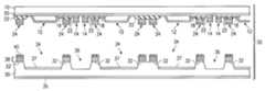
- FIG. 1is a top view of a silicon wafer having MEMS devices formed thereon;
- FIG. 2is a top view of the silicon wafer of FIG. 1 illustrating a sealing ring surrounding each MEMS device on the wafer;
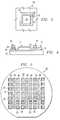
- FIG. 3is a top view of a single MEMS device illustrating the MEMS device, associated bonding pads, and the surrounding sealing ring;
- FIG. 4is a cross section of a single MEMS device illustrating the various layers of the MEMS device
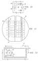
- FIG. 5is a top view of the patterned side of a silicon lid wafer
- FIG. 6is a cross section of the silicon lid wafer of FIG. 5;
- FIG. 7is a cross section of the lid wafer and the device wafer illustrating the mating process which results in vacuum packaged MEMS devices
- FIG. 8is a cross section of the lid wafer prior to formation of spacers on each of the lid sealing rings
- FIG. 9is a cross section of a lid wafer after formation of the spacers on each of the lid sealing rings
- FIG. 10is a schematic diagram of a portion of the lid wafer with a lid sealing ring and spacers formed thereon;
- FIG. 11is a top view of the complete device wafer and lid wafer assembly after removal of the lid wafer area to expose bonding pads for testing devices in the wafer assembly;
- FIG. 12is a schematic diagram of MEMS devices prepared for mating with another integrated circuit device
- FIG. 13is a schematic diagram of a semiconductor device prepared for mating with a MEMS device.
- FIG. 14is a flow chart illustrating the basic steps involved in wafer level vacuum packaging of MEMS devices.
- MEMS devices and certain other inertial MEMS devicesrequire a vacuum environment to attain maximum performance.
- infrared microbolometersrequire an operating pressure of less than 10 millitorr to minimize thermal transfer from the detector elements to the substrate and package walls.
- vacuum compatible materials processes and equipmentmust be used.
- Infrared devicesalso require an optically transparent cover.
- the solution to high packaging costsis to eliminate the traditional individual vacuum packaging of a completed die.
- thisis achieved by moving the packaging step into the wafer fabrication area.
- a lid waferis aligned and mounted to the device wafer with an annular seal ring of solder, or other sealing material, forming an enclosed cell at each die location.
- This lid attachment processis completed in a vacuum environment, leaving each MEMS device in a vacuum cell. Interconnects are brought out under the solder seal ring and are isolated by a dielectric layer.
- Silicon device wafer 10is a standard substrate used for fabrication of integrated circuit devices, MEMS devices or similar devices.
- any suitable substrate materialmay be used.
- a substrate material with integrated circuit readout devices embedded thereinmay be used as device wafer 10 .
- Silicon device wafersusually have many MEMS devices 12 formed thereon using traditional methods of integrated circuit fabrication.
- the present embodiment of the inventionis discussed in terms of vacuum packaging for MEMS devices, the method may be used for vacuum packaging of any integrated circuit device, or similar device, formed on a substrate material and contained within a vacuum package.
- Each MEMS device 12usually has one or more associated bonding pads 14 . Bonding pads 14 provide the electrical connections to MEMS device 12 .
- Bonding pads 14provide the electrical connections to MEMS device 12 .
- each MEMS device 12has two associated bonding pads 14 .
- the bonding padscould exist on one or more sides of MEMS device 12 depending upon the specific application for, and design of, MEMS device 12 .
- MEMS device 12could be a MEMS device or other micro-device formed on a suitable substrate and benefitting from a vacuum package.
- micro-deviceis used herein to refer to these devices including integrated circuit devices, MEMS devices, or similar devices.
- device wafer 10is illustrated having MEMS devices 12 and associated bonding pads 14 .
- sufficient areamust be left in order to place a sealing ring 16 around each MEMS device 12 .
- Sealing ring 16defines the vacuum package around a MEMS device 12 .
- the present embodimentis discussed in terms of one MEMS device 12 , or micro-device, per vacuum package, or vacuum cell, one or more micro-devices may be enclosed in a vacuum cell depending on the requirements, function, and design of the resulting device.
- a single MEMS device 12is illustrated to more completely show the layout on device wafer 10 .
- a lead 18connects each bonding pad 14 to MEMS device 12 .
- a spaceis left between MEMS device 12 and bonding pad 14 to form the device sealing ring 16 .
- lead 18runs beneath fabrication layers to be built within device sealing ring 16 . Since the device sealing ring 16 defines the area of the device wafer 10 within which a vacuum package will be formed, electrical connections are made to bonding pads 14 without affecting the vacuum seal existing around MEMS device 12 .
- Device wafer 10includes a layer of silicon dioxide 20 deposited or grown upon the surface thereof prior to fabrication of MEMS device 12 .
- a lead 18 on a side of the MEMS device 12enables coupling to the bonding pads 14 .
- leads 18could exist on one or more sides of MEMS device 12 .
- Sufficient spaceis provided between MEMS device 12 and bonding pads 14 to allow fabrication of sealing layers for the device sealing ring 16 .
- Bonding pad 14may be comprised of any suitable metal or metals for making subsequent electrical connections.
- the bonding pad 14is comprised of a first layer of titanium, a second layer of palladium, and a final layer of gold. Since bonding pad 14 is deposited on lead 18 , a solder base layer may not be needed for bonding pad 14 .
- Bonding padsare fabricated along with the MEMS device 12 and are discussed here only for completeness. Bonding pads are not part of the vacuum packaging process.
- a dielectric layer 22is formed as the first step of fabricating a device sealing ring 16 (not expressly shown) using integrated circuit fabrication techniques.
- the dielectric layer 22is composed of silicon nitride although any suitable dielectric may be used.
- Dielectric layer 22provides electrical isolation for leads 18 .
- a solder adhesion surface 24is fabricated on the dielectric layer 22 as the next step in completing the device sealing ring 16 .
- Solder adhesion surface 24is illustrated to be comprised of a first layer of titanium, a middle layer of palladium, and a third layer of gold. However, there are many suitable metals or combination of metals available for use in fabricating the solder adhesion surface 24 . Solder adhesion surface 24 may be deposited at the same time as bonding pads 14 .
- a compression sealsuch as an indium compression seal, may be used. If a compression seal is used, then solder adhesion surface 24 is not formed on top of the dielectric layer 22 . At this point, preparation of the sealing ring 16 on the device wafer 10 is complete. Every MEMS device 12 upon device wafer 10 now has a sealing ring 16 prepared to receive a heat activated solder sealed vacuum package lid.
- Lid wafer 30includes a plurality of lid sealing rings 32 corresponding in number to device sealing rings 16 on device wafer 10 .
- Each of the lid sealing rings 32is a mirror image of a device sealing ring 16 so that lid wafer 30 mates with device wafer 10 .
- Cavities 34 and bonding pad channels 36are etched in the lid wafer 30 using an appropriate process such as wet or dry etching.
- the etching process for cavities 34 and bonding pad channels 36may include depositing a layer of silicon nitride and patterning the silicon nitride layer to form an appropriate etch mask. An orientation dependent etch, or other suitable process, is then used to form cavities 34 and bonding pad channels 36 . The silicon nitride layer may be removed before depositing the seal rings 32 . Each of the cavities 34 is surrounded by a lid sealing ring 32 . The function of the cavities 34 is to provide increased volume for a vacuum packaged MEMS device 12 . As discussed below, the increased volume for the vacuum packaged MEMS device 12 provides for a higher vacuum level within the vacuum cell. Cavities 34 may be optional in some embodiments of the present invention that do not require a high vacuum.
- the function of the bonding pad channel 36is to provide clearance over bonding pads 14 so that a dicing saw, etching process, or other suitable process may be used in a later step to open the lid wafer to expose the bonding pads for device testing before dicing of the wafer.
- lid wafer 30there is illustrated a cross section of a portion of lid wafer 30 .
- Lid sealing rings 32are fabricated on the lid wafer 30 to mate with device sealing rings 16 on the device wafer 10 .
- An etching process, or other suitable process,is used to etch the surface of lid wafer 30 creating cavities 34 and bonding pad channels 36 .
- the etching processcreates a cavity 34 on lid wafer 30 corresponding to each MEMS device 12 on device wafer 10 and a bonding pad channel 36 in lid wafer 30 corresponding to each row of bonding pads 14 on device wafer 10 .
- An alternate process of patterning the lid wafer 30includes forming a window wafer which is then bonded to the lid wafer.
- the window wafermay be formed by completely etching cavities 34 and bonding pad channels 36 through a wafer that is then bonded to an unetched lid wafer 30 . This process provides smooth surfaces within cavities 34 and bonding pad channels 36 when bonded to the lid wafer 30 .
- lid wafer 30Another alternate process of patterning lid wafer 30 includes etching the entire surface of the lid wafer leaving lid sealing rings 32 raised above the surface. The complete surface of lid wafer 30 except lid sealing rings 32 would be etched to a predetermined depth.
- An optical coatingmay be necessary on the surface of the lid wafer 30 for optimal performance of MEMS device 12 . If MEMS device 12 is an infrared detector or other optical device, an anti-reflective coating 35 is applied to the outer surface of lid wafer 30 . In addition, the cavities 34 in lid wafer 30 may be coated with an anti-reflective coating 37 .
- Cavities 34represent areas of the lid wafer 30 directly above MEMS device 12 when fabrication is complete thus creating a package for MEMS device 12 . Cavities 34 may be on the order of 0.5 to 0.75 millimeter deep.
- a solder adhesion surface 38is deposited to form lid sealing rings 32 .
- solder adhesion surface 38is not needed if an attachment method is used other than heat activated solder. In the preferred embodiment, heat activated solder is used and, therefore, lid solder adhesion surface 38 is deposited to form lid sealing rings 32 .
- Lid solder adhesion surface 38is comprised of any combination of metal or metal alloys that will provide a surface wettable by the solder, and a secure attachment to device wafer 10 .
- the lid solder adhesion surface 38is comprised of a first layer of titanium, followed by a middle layer of palladium, and an outer layer of gold.
- a solder layer 40is deposited on lid solder adhesion surface 38 . If a sealing method other than heat activated solder is used, the solder layer 40 is replaced by a material necessary to obtain a vacuum tight seal. In an alternative embodiment, an indium compression seal is used. However, in the preferred embodiment, a heat activated solder layer 40 is used. Solder layer 40 may be deposited through traditional integrated circuit fabrication techniques or other suitable deposition processes. For example, lid wafer 30 is electroplated resulting in solder layer 40 being deposited upon lid solder adhesion surface 38 . Another method of depositing solder layer 40 includes using electroless plating. Another method of depositing solder layer 40 includes using vacuum deposition.
- solder layer 40includes using a preformed, prepunched solder layer which is aligned over lid solder adhesion surfaces 38 and attached thereto. Any suitable method of attachment may be used including spot welding the preformed, prepunched solder layer to lid solder adhesion surfaces 38 .
- a solder ball methodcould be used to deposit solder layer 40 .
- the solder ball methodincludes creating a template with a plurality of discrete holes where solder would be deposited. The template, with solder balls in the holes, is then aligned and placed on lid wafer 30 . The solder balls are then released from the template and attached to lid solder adhesion surfaces 38 .
- solder layer 40may be comprised of any appropriate material such as an indium compression seal, indium solder, metal solder, metal alloy solder, or solder balls. Although the preferred embodiment deposits solder layer 40 on lid solder adhesion surface 38 , solder layer 40 could also be deposited on solder adhesion surface 24 on device wafer 10 .
- the lid wafer 30is placed in an assembly holder (not expressly shown) with the solder layer 40 facing up.
- Device wafer 10is aligned over lid wafer 30 such that device sealing rings 16 are aligned over the corresponding lid sealing rings 32 .
- solder layer 40is deposited on solder adhesion surface 24 on device wafer 10
- the device waferis placed in an assembly holder with the solder layer 40 facing up, and the lid wafer 30 is aligned over device wafer 10 .
- Lid wafer 30 and device wafer 10are held in alignment with a gap to allow outgassing of all surface areas.
- the gapmay be on the order of two millimeters.
- Assembly 50thus includes lid wafer 30 and device wafer 10 aligned in an assembly holder with a gap to allow outgassing.
- the gapprovides for a more complete evacuation of each vacuum cell and, thus, a higher vacuum level in the resulting vacuum packaged MEMS devices 12 .
- Assembly 50is placed in a vacuum furnace.
- the vacuum furnaceis evacuated to a minimum pressure level on the order of 2 ⁇ 10 ⁇ 7 torr.
- the vacuum furnaceis then heated to a level just below the melting point of the solder layer 40 .
- the vacuum furnaceis heated to approximately 275° C.
- the vacuum furnace temperatureis dependent upon the melting point of solder layer 40 .
- Assembly 50is held in the vacuum furnace for a period sufficient to allow outgassing of all surfaces. This period may be on the order of several hours. The holding period is determined by the final vacuum pressure required within the vacuum packaged MEMS device.
- the vacuum furnace temperatureis raised to the melting point of solder layer 40 .
- solder layer 40melts, a short period of time is allowed for outgassing of the solder and then device wafer 10 is brought into contact with lid wafer 30 creating a vacuum seal between lid sealing rings 32 and device sealing rings 16 .
- all MEMS devices 12 on device wafer 10are now enclosed within a vacuum package.
- sealing layer 40is not heat activated, a vacuum chamber may be used in place of a vacuum furnace to provide the appropriate vacuum environment. In that situation, melting of solder layer 40 would not be necessary. An application of force may then be used to seal the device wafer 10 with the lid wafer 30 .
- FIGS. 8, 9 , and 10illustrate solder thickness control for maintaining a uniform solder thickness for all MEMS devices 12 on assembly 50 . By maintaining a uniform solder thickness, proper vacuum seals and adequate vacuums will exist for each vacuum packaged MEMS device 12 on device wafer 10 .
- lid wafer 30after cavities 34 and bonding pad channels 36 have been etched leaving lid sealing rings 32 surrounding each cavity 34 .
- a layer of silicon nitride 102is deposited on the surface of lid wafer 30 and patterned to form an etch mask.
- An orientation dependent etch, or other suitable process,is used to form cavities 34 and bonding pad channels 36 resulting in the configuration of lid wafer 30 shown in FIG. 8 .
- the lid wafer 30having spacers 100 formed on the lid sealing rings 32 .
- Silicon nitride layer 102is patterned and etched using any suitable etching process to form small islands of material defining the spacers 100 .
- the small islands of silicon nitride 102may be on the order of 20 microns in diameter.
- the number of islands of silicon nitride 102 formed on lid sealing rings 32is determined to insure a minimum thickness of the solder layer 40 on all lid sealing rings 32 .
- Lid wafer 30is then exposed to an orientation dependent etch, or any other suitable patterning technique, to form spacers 100 on lid sealing rings 32 .
- the nitride on top of each spacer 100may remain. However, the nitride layer may be removed if necessary.
- lid sealing rings 32are prepared with a solder adhesion surface 38 and solder layer 40 as discussed with reference to FIG. 6 and FIG. 7 .
- Spacers 100are placed in lid sealing ring 32 to produce a uniform thickness of solder. Spacers 100 may be on the order of 5 to 20 microns high. Any suitable process may be used to form spacers 100 including attaching a small dot of material, such as silicon, to the surface of lid sealing ring 32 rather than etching the surface of lid sealing ring 32 . Although the process of forming spacers 100 has been discussed in relation to vacuum packaging of MEMS devices 12 , spacers 100 may be incorporated into any wafer level packaging process where a lid wafer is mated with a device wafer, regardless of the underlying components or devices.
- pressure levels as low as 5 millitorrhave been achieved although lower pressure levels are possible.
- vacuum pressureBy minimizing the vacuum pressure, performance of certain MEMS devices is maximized.
- infrared microbolometersrequire an operating pressure of less than 10 millitorr to minimize thermal transfer from the detector elements to the substrate or package walls.
- probe channels 54are formed in lid wafer 30 by removing the lid wafer 30 over bonding pad channel 36 . After probe channels 54 have been formed in lid wafer 30 , bonding pads 14 are accessible through the probe channels.
- Vacuum package areas 52illustrate the areas between lid wafer 30 and device wafer 10 where a vacuum package exists. Within each vacuum package area 52 is one or more MEMS device 12 .
- Probe channels 54are preferably formed by sawing a channel through the lid wafer 30 over the previously etched bonding pad channels 36 . Probe channels 54 may also be formed by an etching process or other suitable technique.
- bonding pads 14are exposed. Bonding pads 14 can then be used to test each individual vacuum packaged MEMS device 12 on device wafer 10 using traditional integrated circuit bulk testing procedures which include probing each bonding pad 14 .
- An important advantage of the present inventionis that the vacuum packaged MEMS devices 12 may be tested at the wafer level thus minimizing the cost of verifying the operational integrity of each individual vacuum packaged MEMS device 12 .
- the device wafer 10is diced by sawing through probe channels 54 between bonding pads 14 .
- a dicing sawis run between all vacuum package areas 52 .
- the dicing of assembly 50may be accomplished by using traditional methods of dicing silicon wafers with completed integrated circuits.
- vacuum packaging MEMS devices 12 at the wafer leveltraditional methods of handling integrated circuit devices may be used since the vacuum package provides protection to the delicate MEMS device 12 .
- the completed die representing a vacuum packaged MEMS device 12may be mounted by chip-on-board methods or injection molded into a plastic package. In addition, the completed die may be placed in a non-vacuum package with other components.
- FIG. 12 and FIG. 13illustrate an alternate embodiment of the present invention that enables a device wafer with MEMS devices to be mated with a lid wafer containing other semiconductor devices.
- CMOSComplementary Metal Oxide Semiconductor
- the CMOS circuitrygenerally cannot be exposed to temperatures above approximately 400° C. This temperature limitation may exist for certain other integrated circuit (IC) devices.
- ICintegrated circuit
- Typical MEMS fabrication techniquesoften use temperatures in excess of 400° C.
- One solution to this problemis to separately fabricate the MEMS device and the CMOS device so that the CMOS device is not exposed to temperatures above 400° C.
- a MEMS die and a CMOS dieare then placed in a package and electrically connected. This process requires expensive individual die handling.
- MEMS devicesare fabricated on a device wafer and the CMOS devices are fabricated on a lid wafer. These wafers are then vacuum sealed together to produce a wafer with many vacuum packaged MEMS/CMOS devices.
- MEMS devicesare produced without processing limitations.
- Another advantageis that wafer losses in MEMS device fabrication do not result in the loss of a fully fabricated IC wafer. Since the alternate embodiment uses CMOS or other IC devices formed on a lid wafer, the alternate embodiment may not be suitable for use with MEMS devices requiring an optically transparent lid.
- MEMS devicebenefitting from the alternate process is a mechanical MEMS device connected to a CMOS or other IC device to form a complete, operating device.
- CMOScomplementary metal-oxide-semiconductor
- the alternate embodimentwill be discussed with a single MEMS device 12 and a single CMOS device vacuum packaged together, one or more MEMS devices 12 and one or more CMOS devices could be incorporated into a single vacuum packaged die.
- wafer fabrication designmay not require every MEMS device to be packaged with a CMOS device. For instance, one-half of the resulting dies may be MEMS only vacuum packaged devices and the other half may be MEMS/CMOS vacuum packaged devices.
- FIG. 12there is illustrated a portion of device wafer 10 having a MEMS device 12 .
- a typical device wafer 10has many MEMS devices 12 .
- One or more device mating pads 70are coupled to MEMS device 12 through leads 72 .
- Device mating pads 70are used to provide an electrical connection between MEMS device 12 and a CMOS or other integrated circuit (IC) device on a lid wafer.
- Device mating pads 70may be comprised of a solder adhesion surface as described with reference to bonding pads 14 and are located within the area bounded by device sealing ring 16 and, thus, within the resulting vacuum package.
- Device sealing ring 16is prepared for mating with a lid sealing ring on a lid wafer 30 as previously described.
- device sealing ring 16includes a solder adhesion surface deposited and formed thereon. Since the alternate embodiment does not utilize bonding pads coupled to MEMS device 12 for providing electrical connections to the completed vacuum packaged die, a dielectric layer is not necessary for device sealing ring 16 .
- the area bounded by device sealing ring 16represents the area inside a vacuum package. Note that empty space is left within the vacuum area to accommodate the CMOS or other IC device formed on lid wafer 30 .
- lid wafer 30with a CMOS or other IC device 80 formed thereon.
- Lid wafer 30may have many CMOS devices 80 .
- Lid sealing ring 32defines the area for forming lid solder adhesion surface 38 as previously described.
- One or more lid mating pads 82are fabricated on the lid wafer 30 . These lid mating pads 82 are a mirror image of device mating pads 70 so that when the device wafer 10 and the lid wafer 30 are properly aligned, device mating pads 70 and lid mating pads 82 will make contact thus providing electrical connections between MEMS device 12 and CMOS device 80 .
- Lid mating pads 82are connected to CMOS device 80 through leads 84 .
- the lid mating pads 82are comprised of a solder adhesion surface.
- one or more package bonding pads 86are connected to CMOS device 80 through leads 88 .
- leads 88pass under the lid sealing ring 32 .
- the lid sealing ring 32has a layer of silicon dioxide providing electrical insulation between leads 88 and the solder seal ring formed by device sealing ring 16 and lid sealing ring 32 .
- Package bonding pads 86provide the electrical connections for the resulting vacuum packaged device.
- lid sealing ring 32includes a layer of solder deposited on a lid solder adhesion surface. However, the solder layer could be deposited on either the properly prepared device sealing ring 16 or the properly prepared lid sealing ring 32 .
- a solder layeris also deposited on either device mating pads 70 or lid mating pads 82 so that a permanent electrical connection is made when device wafer 10 is mated with lid wafer 30 .
- the soldermay be any suitable metal or metal alloy.
- a lower vacuum in vacuum packaged MEMS device 12may be expected for solder with a higher melting point since a more complete outgassing of package surface areas will occur.
- the vacuum within vacuum packaged MEMS device 12is enhanced in the case of a solder with a low melting point by applying the solder to the lid wafer 30 and heating the device wafer 10 separately to a higher temperature than the solder melting point so as to obtain a more complete surface outgassing of device wafer 10 .
- the desired vacuum level within the completed vacuum packaged MEMS device 12 and the temperature tolerance of lid wafer 30determine the type of solder to be used, the furnace temperatures, and the furnace vacuum level.
- the lid waferis placed in an assembly holder and device wafer 10 is aligned over the lid wafer. If the mating process utilizes a furnace temperature that will not damage CMOS devices 80 on lid wafer 30 , the device wafer 10 and lid wafer 30 assembly are mated using the previously described process. If a furnace temperature will be utilized that may damage CMOS devices 80 on lid wafer 30 , device wafer 10 may be separately heated. Device wafer 10 is then brought into alignment with lid wafer 30 followed by contacting the two wafers in a vacuum environment to produce vacuum packaged MEMS devices 12 .
- probe access channelsare opened above package bonding pads 86 (in this case, through device wafer 10 ) to allow testing of vacuum packaged MEMS devices 12 utilizing bulk IC testing procedures. After all dies on the completed assembly are tested, the completed assembly is diced into individual dies.
- an area in device wafer 10is etched to provide a cavity to increase the surface-to-volume ratio of the resulting vacuum package.
- a flow chartillustrates the steps involved in vacuum packaging integrated circuit components during fabrication.
- a plurality of MEMS devices 12is formed on device wafer 10 .
- the methodthen proceeds to step 202 where a dielectric layer 22 is formed between the perimeter of each MEMS device 12 and associated bonding pads 14 .
- Dielectric layer 22forms a continuous ring surrounding MEMS device 12 .
- a dielectric layer inherent in the structure of the MEMS device 12may also be used.
- the methodthen proceeds to step 204 where a sealing ring is formed on dielectric layer 22 .
- Sealing ring 16may include a lid solder adhesion surface to facilitate the mating of the device wafer 10 with a lid wafer 30 using a heat activated solder.
- the methodthen proceeds to step 206 where a plurality of lid sealing rings 32 is formed corresponding in location and number to device sealing rings 16 .
- the methodthen proceeds to step 208 where a sealing layer is formed on each lid sealing ring 32 .
- the sealing layermay be comprised of a heat activated solder, but may be composed of any appropriate sealing material. If MEMS device 12 has a support layer for any moving portions of MEMS device 12 , the support layer is removed with an appropriate process, such as an etch process, prior to proceeding to step 210 .
- step 210the device wafer 10 is aligned with the lid wafer 30 .
- each device sealing ring 16is aligned with its corresponding lid sealing ring 32 .
- step 212the device wafer 10 is mated with the lid wafer 30 in a vacuum environment thus creating a plurality of vacuum packaged MEMS devices 12 .
- step 214each vacuum packaged MEMS device 12 is tested using traditional integrated circuit testing procedures. In order to facilitate testing, probe access channels are opened above bonding pads 14 coupled to vacuum packaged MEMS devices 12 .
- step 216the completed assembly 50 is diced using traditional integrated circuit dicing techniques.
Landscapes
- Engineering & Computer Science (AREA)
- Microelectronics & Electronic Packaging (AREA)
- Computer Hardware Design (AREA)
- Micromachines (AREA)
Abstract
Description
Claims (23)
Priority Applications (6)
| Application Number | Priority Date | Filing Date | Title |
|---|---|---|---|
| US09/496,826US6479320B1 (en) | 2000-02-02 | 2000-02-02 | Vacuum package fabrication of microelectromechanical system devices with integrated circuit components |
| EP01906897AEP1272422A2 (en) | 2000-02-02 | 2001-02-01 | Vacuum package fabrication of microelectromechanical system devices with integrated circuit components |
| JP2001556778AJP2003531475A (en) | 2000-02-02 | 2001-02-01 | Manufacture of vacuum package for micro-electromechanical system devices with integrated circuit components |
| AU2001234750AAU2001234750A1 (en) | 2000-02-02 | 2001-02-01 | Vacuum package fabrication of microelectromechanical system devices with integrated circuit components |
| PCT/US2001/003371WO2001056921A2 (en) | 2000-02-02 | 2001-02-01 | Vacuum package fabrication of microelectromechanical system devices with integrated circuit components |
| KR1020027009867AKR20030023613A (en) | 2000-02-02 | 2001-02-01 | Vacuum Package Fabrication of Microelectromechanical System Devices with Integrated Circuit Components |
Applications Claiming Priority (1)
| Application Number | Priority Date | Filing Date | Title |
|---|---|---|---|
| US09/496,826US6479320B1 (en) | 2000-02-02 | 2000-02-02 | Vacuum package fabrication of microelectromechanical system devices with integrated circuit components |
Publications (1)
| Publication Number | Publication Date |
|---|---|
| US6479320B1true US6479320B1 (en) | 2002-11-12 |
Family
ID=23974308
Family Applications (1)
| Application Number | Title | Priority Date | Filing Date |
|---|---|---|---|
| US09/496,826Expired - LifetimeUS6479320B1 (en) | 2000-02-02 | 2000-02-02 | Vacuum package fabrication of microelectromechanical system devices with integrated circuit components |
Country Status (1)
| Country | Link |
|---|---|
| US (1) | US6479320B1 (en) |
Cited By (118)
| Publication number | Priority date | Publication date | Assignee | Title |
|---|---|---|---|---|
| US20030111441A1 (en)* | 2000-06-28 | 2003-06-19 | Institut National D'optique | Miniature microdevice package and process for making thereof |
| US6586831B2 (en)* | 2000-02-02 | 2003-07-01 | Raytheon Company | Vacuum package fabrication of integrated circuit components |
| US20030183920A1 (en)* | 2002-03-28 | 2003-10-02 | Goodrich Joel Lee | Hermetic electric component package |
| US6777263B1 (en)* | 2003-08-21 | 2004-08-17 | Agilent Technologies, Inc. | Film deposition to enhance sealing yield of microcap wafer-level package with vias |
| US20040191957A1 (en)* | 2003-03-26 | 2004-09-30 | Northrop Grumman Corporation | Wafer scale package and method of assembly |
| US20040219764A1 (en)* | 2003-05-02 | 2004-11-04 | Raytheon Company | Vacuum package fabrication of integrated circuit components |
| US20040222468A1 (en)* | 2003-05-07 | 2004-11-11 | Dcamp Jon B. | Methods and apparatus for particle reduction in MEMS devices |
| US20050017329A1 (en)* | 2003-06-10 | 2005-01-27 | California Institute Of Technology | Multiple internal seal ring micro-electro-mechanical system vacuum package |
| US20050079684A1 (en)* | 2002-01-29 | 2005-04-14 | Wai Mun Chong | Method of manufacturing an accelerometer |
| US20050094242A1 (en)* | 2003-11-01 | 2005-05-05 | Fusao Ishii | Vacuum packaged micromirror arrays and methods of manufacturing the same |
| US20050142685A1 (en)* | 2003-12-15 | 2005-06-30 | Dalsa Semiconductor Inc. | Hermetic wafer-level packaging for MEMS devices with low-temperature metallurgy |
| US20050156320A1 (en)* | 2000-12-29 | 2005-07-21 | Stmicroelectronics S.R.I. | Integrated device including connections on a separate wafer |
| US20050170656A1 (en)* | 2003-10-20 | 2005-08-04 | Nasiri Steven S. | Vertical integration of a MEMS structure with electronics in a hermetically sealed cavity |
| US20050166677A1 (en)* | 2004-02-02 | 2005-08-04 | Nasiri Steven S. | Vertically integrated MEMS structure with electronics in a hermetically sealed cavity |
| US20050173769A1 (en)* | 2004-02-09 | 2005-08-11 | Don Michael | Package for a micro-electro mechanical device |
| US20050253283A1 (en)* | 2004-05-13 | 2005-11-17 | Dcamp Jon B | Getter deposition for vacuum packaging |
| WO2005038909A3 (en)* | 2003-10-17 | 2005-11-24 | Raytheon Co | Integrated package design for a radiation sensing device and manufacturing method |
| US20050285541A1 (en)* | 2003-06-23 | 2005-12-29 | Lechevalier Robert E | Electron beam RF amplifier and emitter |
| US20060012021A1 (en)* | 2004-07-13 | 2006-01-19 | Larson John D Iii | Film bulk acoustic resonator package and method of fabricating same |
| US20060063357A1 (en)* | 2004-09-20 | 2006-03-23 | Jun Young Yang | Singulation method used in image sensor packaging process and support for use therein |
| US20060071736A1 (en)* | 2004-10-01 | 2006-04-06 | Ruby Richard C | Acoustic resonator performance enhancement using alternating frame structure |
| US20060088980A1 (en)* | 2004-10-27 | 2006-04-27 | Chien-Hua Chen | Method of singulating electronic devices |
| US20060128058A1 (en)* | 2004-12-15 | 2006-06-15 | Dungan Thomas E | Wafer bonding of micro-electro mechanical systems to active circuitry |
| US20060125084A1 (en)* | 2004-12-15 | 2006-06-15 | Fazzio Ronald S | Integration of micro-electro mechanical systems and active circuitry |
| US20060141650A1 (en)* | 2004-12-27 | 2006-06-29 | Samsung Electronics Co., Ltd. | MEMS device package and method for manufacturing the same |
| US20060208326A1 (en)* | 2005-03-18 | 2006-09-21 | Nasiri Steven S | Method of fabrication of ai/ge bonding in a wafer packaging environment and a product produced therefrom |
| US20070004079A1 (en)* | 2005-06-30 | 2007-01-04 | Geefay Frank S | Method for making contact through via contact to an offset contactor inside a cap for the wafer level packaging of FBAR chips |
| US20070000976A1 (en)* | 2005-06-30 | 2007-01-04 | Arana Leonel R | Electrically-isolated interconnects and seal rings in packages using a solder preform |
| US20070048898A1 (en)* | 2005-08-26 | 2007-03-01 | Innovative Micro Technology | Wafer level hermetic bond using metal alloy with raised feature |
| US20070085447A1 (en)* | 2005-10-18 | 2007-04-19 | Larson John D Iii | Acoustic galvanic isolator incorporating single insulated decoupled stacked bulk acoustic resonator with acoustically-resonant electrical insulator |
| US20070087462A1 (en)* | 2005-10-14 | 2007-04-19 | Haluzak Charles C | Method of forming a device package having edge interconnect pad |
| US20070117275A1 (en)* | 2005-11-22 | 2007-05-24 | Honeywell International Inc. | Mems device packaging methods |
| US20070128828A1 (en)* | 2005-07-29 | 2007-06-07 | Chien-Hua Chen | Micro electro-mechanical system packaging and interconnect |
| US20070170359A1 (en)* | 2006-01-26 | 2007-07-26 | Syllaios Athanasios J | Systems and methods for integrating focal plane arrays |
| US20070170360A1 (en)* | 2006-01-26 | 2007-07-26 | Gooch Roland W | Systems and methods for bonding |
| US20070170363A1 (en)* | 2006-01-26 | 2007-07-26 | Schimert Thomas R | Infrared detector elements and methods of forming same |
| WO2007121992A1 (en)* | 2006-04-25 | 2007-11-01 | Fraunhofer-Gesellschaft zur Förderung der angewandten Forschung e.V. | Housing with an electric circuit |
| US7332985B2 (en) | 2003-10-30 | 2008-02-19 | Avago Technologies Wireless Ip (Singapore) Pte Ltd. | Cavity-less film bulk acoustic resonator (FBAR) devices |
| US20080048120A1 (en)* | 2006-08-28 | 2008-02-28 | Gooch Roland W | Surface mounted infrared image detector systems and associated methods |
| US7362198B2 (en) | 2003-10-30 | 2008-04-22 | Avago Technologies Wireless Ip (Singapore) Pte. Ltd | Pass bandwidth control in decoupled stacked bulk acoustic resonator devices |
| US7367095B2 (en) | 2003-10-30 | 2008-05-06 | Avago Technologies General Ip Pte Ltd | Method of making an acoustically coupled transformer |
| US7369013B2 (en) | 2005-04-06 | 2008-05-06 | Avago Technologies Wireless Ip Pte Ltd | Acoustic resonator performance enhancement using filled recessed region |
| US7388455B2 (en) | 2003-10-30 | 2008-06-17 | Avago Technologies Wireless Ip Pte Ltd | Film acoustically-coupled transformer with increased common mode rejection |
| US7391286B2 (en) | 2005-10-06 | 2008-06-24 | Avago Wireless Ip Pte Ltd | Impedance matching and parasitic capacitor resonance of FBAR resonators and coupled filters |
| US7423503B2 (en) | 2005-10-18 | 2008-09-09 | Avago Technologies Wireless Ip (Singapore) Pte. Ltd. | Acoustic galvanic isolator incorporating film acoustically-coupled transformer |
| US7424772B2 (en) | 2003-10-30 | 2008-09-16 | Avago Technologies Wireless Ip (Singapore) Pte. Ltd. | Stacked bulk acoustic resonator band-pass filter with controllable pass bandwidth |
| US7427819B2 (en) | 2005-03-04 | 2008-09-23 | Avago Wireless Ip Pte Ltd | Film-bulk acoustic wave resonator with motion plate and method |
| US7436269B2 (en) | 2005-04-18 | 2008-10-14 | Avago Technologies Wireless Ip (Singapore) Pte. Ltd. | Acoustically coupled resonators and method of making the same |
| US7463499B2 (en) | 2005-10-31 | 2008-12-09 | Avago Technologies General Ip (Singapore) Pte Ltd. | AC-DC power converter |
| EP2011762A2 (en) | 2007-07-02 | 2009-01-07 | Denso Corporation | Semiconductor device with a sensor connected to an external element |
| US7479685B2 (en) | 2006-03-10 | 2009-01-20 | Avago Technologies General Ip (Singapore) Pte. Ltd. | Electronic device on substrate with cavity and mitigated parasitic leakage path |
| US20090042328A1 (en)* | 2001-07-24 | 2009-02-12 | Nichia Corporation | Semiconductor light emitting device |
| US7508286B2 (en) | 2006-09-28 | 2009-03-24 | Avago Technologies Wireless Ip (Singapore) Pte. Ltd. | HBAR oscillator and method of manufacture |
| US7525398B2 (en) | 2005-10-18 | 2009-04-28 | Avago Technologies General Ip (Singapore) Pte. Ltd. | Acoustically communicating data signals across an electrical isolation barrier |
| US7561009B2 (en) | 2005-11-30 | 2009-07-14 | Avago Technologies General Ip (Singapore) Pte. Ltd. | Film bulk acoustic resonator (FBAR) devices with temperature compensation |
| US7612636B2 (en) | 2006-01-30 | 2009-11-03 | Avago Technologies Wireless Ip (Singapore) Pte. Ltd. | Impedance transforming bulk acoustic wave baluns |
| US7629865B2 (en) | 2006-05-31 | 2009-12-08 | Avago Technologies Wireless Ip (Singapore) Pte. Ltd. | Piezoelectric resonator structures and electrical filters |
| US7675390B2 (en) | 2005-10-18 | 2010-03-09 | Avago Technologies Wireless Ip (Singapore) Pte. Ltd. | Acoustic galvanic isolator incorporating single decoupled stacked bulk acoustic resonator |
| US7718965B1 (en) | 2006-08-03 | 2010-05-18 | L-3 Communications Corporation | Microbolometer infrared detector elements and methods for forming same |
| US7732977B2 (en) | 2008-04-30 | 2010-06-08 | Avago Technologies Wireless Ip (Singapore) | Transceiver circuit for film bulk acoustic resonator (FBAR) transducers |
| US7737807B2 (en) | 2005-10-18 | 2010-06-15 | Avago Technologies Wireless Ip (Singapore) Pte. Ltd. | Acoustic galvanic isolator incorporating series-connected decoupled stacked bulk acoustic resonators |
| US7746677B2 (en) | 2006-03-09 | 2010-06-29 | Avago Technologies Wireless Ip (Singapore) Pte. Ltd. | AC-DC converter circuit and power supply |
| CN101798054A (en)* | 2010-05-10 | 2010-08-11 | 北京广微积电科技有限公司 | Wafer-level vacuum encapsulating method for micro-electromechanical device |
| US7791435B2 (en) | 2007-09-28 | 2010-09-07 | Avago Technologies Wireless Ip (Singapore) Pte. Ltd. | Single stack coupled resonators having differential output |
| US7791434B2 (en) | 2004-12-22 | 2010-09-07 | Avago Technologies Wireless Ip (Singapore) Pte. Ltd. | Acoustic resonator performance enhancement using selective metal etch and having a trench in the piezoelectric |
| US7802349B2 (en) | 2003-03-07 | 2010-09-28 | Avago Technologies Wireless Ip (Singapore) Pte. Ltd. | Manufacturing process for thin film bulk acoustic resonator (FBAR) filters |
| US20100244159A1 (en)* | 2009-03-30 | 2010-09-30 | Freescale Semiconductor, Inc. | Eutectic flow containment in a semiconductor fabrication process |
| US20100258950A1 (en)* | 2009-04-14 | 2010-10-14 | Gang Li | Package with semiconductor device and integrated circuit mounted therein and method for manufacturing such package |
| US20100308450A1 (en)* | 2004-12-10 | 2010-12-09 | Ipdia | Integrated package |
| US7855618B2 (en) | 2008-04-30 | 2010-12-21 | Avago Technologies Wireless Ip (Singapore) Pte. Ltd. | Bulk acoustic resonator electrical impedance transformers |
| US20100327443A1 (en)* | 2008-02-22 | 2010-12-30 | Barun Electronics, Co., Ltd. | Joining structure and a substrate-joining method using the same |
| US7868522B2 (en) | 2005-09-09 | 2011-01-11 | Avago Technologies Wireless Ip (Singapore) Pte. Ltd. | Adjusted frequency temperature coefficient resonator |
| US20110061460A1 (en)* | 2009-09-11 | 2011-03-17 | Invensense, Inc | Extension -mode angular velocity sensor |
| CN102180436A (en)* | 2007-07-02 | 2011-09-14 | 株式会社电装 | Semiconductor device and manufacturing method of the same |
| US8153980B1 (en) | 2006-11-30 | 2012-04-10 | L-3 Communications Corp. | Color correction for radiation detectors |
| US8193877B2 (en) | 2009-11-30 | 2012-06-05 | Avago Technologies Wireless Ip (Singapore) Pte. Ltd. | Duplexer with negative phase shifting circuit |
| US8248185B2 (en) | 2009-06-24 | 2012-08-21 | Avago Technologies Wireless Ip (Singapore) Pte. Ltd. | Acoustic resonator structure comprising a bridge |
| WO2012100361A3 (en)* | 2011-01-27 | 2012-11-15 | Sensirion Ag | Method for manufacturing a sensor chip comprising a device for testing it |
| US8350445B1 (en) | 2011-06-16 | 2013-01-08 | Avago Technologies Wireless Ip (Singapore) Pte. Ltd. | Bulk acoustic resonator comprising non-piezoelectric layer and bridge |
| CN102923638A (en)* | 2012-11-08 | 2013-02-13 | 姜利军 | Hermetic sealing assembly and sealing method |
| US8567246B2 (en) | 2010-10-12 | 2013-10-29 | Invensense, Inc. | Integrated MEMS device and method of use |
| US8575820B2 (en) | 2011-03-29 | 2013-11-05 | Avago Technologies General Ip (Singapore) Pte. Ltd. | Stacked bulk acoustic resonator |
| US8617934B1 (en) | 2000-11-28 | 2013-12-31 | Knowles Electronics, Llc | Methods of manufacture of top port multi-part surface mount silicon condenser microphone packages |
| US8624385B1 (en) | 2000-11-28 | 2014-01-07 | Knowles Electronics, Llc | Top port surface mount silicon condenser microphone package |
| US8729695B2 (en) | 2009-09-25 | 2014-05-20 | Agency For Science, Technology And Research | Wafer level package and a method of forming a wafer level package |
| US8765514B1 (en) | 2010-11-12 | 2014-07-01 | L-3 Communications Corp. | Transitioned film growth for conductive semiconductor materials |
| US8796904B2 (en) | 2011-10-31 | 2014-08-05 | Avago Technologies General Ip (Singapore) Pte. Ltd. | Bulk acoustic resonator comprising piezoelectric layer and inverse piezoelectric layer |
| US8860409B2 (en) | 2011-01-11 | 2014-10-14 | Invensense, Inc. | Micromachined resonant magnetic field sensors |
| US8902023B2 (en) | 2009-06-24 | 2014-12-02 | Avago Technologies General Ip (Singapore) Pte. Ltd. | Acoustic resonator structure having an electrode with a cantilevered portion |
| US8922302B2 (en) | 2011-08-24 | 2014-12-30 | Avago Technologies General Ip (Singapore) Pte. Ltd. | Acoustic resonator formed on a pedestal |
| US8947081B2 (en) | 2011-01-11 | 2015-02-03 | Invensense, Inc. | Micromachined resonant magnetic field sensors |
| US20150048509A1 (en)* | 2013-08-16 | 2015-02-19 | Globalfoundries Singapore Pte. Ltd. | Cmos compatible wafer bonding layer and process |
| US8962443B2 (en) | 2011-01-31 | 2015-02-24 | Avago Technologies General Ip (Singapore) Pte. Ltd. | Semiconductor device having an airbridge and method of fabricating the same |
| US8981876B2 (en) | 2004-11-15 | 2015-03-17 | Avago Technologies General Ip (Singapore) Pte. Ltd. | Piezoelectric resonator structures and electrical filters having frame elements |
| US9048812B2 (en) | 2011-02-28 | 2015-06-02 | Avago Technologies General Ip (Singapore) Pte. Ltd. | Bulk acoustic wave resonator comprising bridge formed within piezoelectric layer |
| US9078063B2 (en) | 2012-08-10 | 2015-07-07 | Knowles Electronics, Llc | Microphone assembly with barrier to prevent contaminant infiltration |
| US9083302B2 (en) | 2011-02-28 | 2015-07-14 | Avago Technologies General Ip (Singapore) Pte. Ltd. | Stacked bulk acoustic resonator comprising a bridge and an acoustic reflector along a perimeter of the resonator |
| US9097524B2 (en) | 2009-09-11 | 2015-08-04 | Invensense, Inc. | MEMS device with improved spring system |
| US9136818B2 (en) | 2011-02-28 | 2015-09-15 | Avago Technologies General Ip (Singapore) Pte. Ltd. | Stacked acoustic resonator comprising a bridge |
| US9148117B2 (en) | 2011-02-28 | 2015-09-29 | Avago Technologies General Ip (Singapore) Pte. Ltd. | Coupled resonator filter comprising a bridge and frame elements |
| US9154112B2 (en) | 2011-02-28 | 2015-10-06 | Avago Technologies General Ip (Singapore) Pte. Ltd. | Coupled resonator filter comprising a bridge |
| US20150287655A1 (en)* | 2014-04-08 | 2015-10-08 | Freescale Semiconductor, Inc. | Semiconductor wafer and method of concurrently testing circuits formed thereon |
| US9203374B2 (en) | 2011-02-28 | 2015-12-01 | Avago Technologies General Ip (Singapore) Pte. Ltd. | Film bulk acoustic resonator comprising a bridge |
| US9227839B2 (en) | 2014-05-06 | 2016-01-05 | Raytheon Company | Wafer level packaged infrared (IR) focal plane array (FPA) with evanescent wave coupling |
| US9243316B2 (en) | 2010-01-22 | 2016-01-26 | Avago Technologies General Ip (Singapore) Pte. Ltd. | Method of fabricating piezoelectric material with selected c-axis orientation |
| US9374643B2 (en) | 2011-11-04 | 2016-06-21 | Knowles Electronics, Llc | Embedded dielectric as a barrier in an acoustic device and method of manufacture |
| US20160185594A1 (en)* | 2014-10-13 | 2016-06-30 | Infineon Technologies Dresden Gmbh | Systems and methods for horizontal integration of acceleration sensor structures |
| US9425764B2 (en) | 2012-10-25 | 2016-08-23 | Avago Technologies General Ip (Singapore) Pte. Ltd. | Accoustic resonator having composite electrodes with integrated lateral features |
| US9444426B2 (en) | 2012-10-25 | 2016-09-13 | Avago Technologies General Ip (Singapore) Pte. Ltd. | Accoustic resonator having integrated lateral feature and temperature compensation feature |
| CN106098568A (en)* | 2015-05-01 | 2016-11-09 | 颀邦科技股份有限公司 | Semiconductor package manufacturing process with hollow cavity |
| US9570321B1 (en) | 2015-10-20 | 2017-02-14 | Raytheon Company | Use of an external getter to reduce package pressure |
| US9664750B2 (en) | 2011-01-11 | 2017-05-30 | Invensense, Inc. | In-plane sensing Lorentz force magnetometer |
| US20170174503A1 (en)* | 2015-12-18 | 2017-06-22 | Samsung Electro-Mechanics Co., Ltd. | Wafer level package and method of manufacturing the same |
| US9754922B2 (en) | 2015-02-11 | 2017-09-05 | Invensense, Inc. | 3D integration using Al—Ge eutectic bond interconnect |
| US9794661B2 (en) | 2015-08-07 | 2017-10-17 | Knowles Electronics, Llc | Ingress protection for reducing particle infiltration into acoustic chamber of a MEMS microphone package |
| US9991868B1 (en) | 2014-04-14 | 2018-06-05 | Hrl Laboratories, Llc | Micro-resonator having lid-integrated electrode |
| US10192850B1 (en) | 2016-09-19 | 2019-01-29 | Sitime Corporation | Bonding process with inhibited oxide formation |
| US11117796B2 (en)* | 2014-01-16 | 2021-09-14 | Taiwan Semiconductor Manufacturing Company, Ltd. | MEMS devices including MEMS dies and connectors thereto |
Citations (53)
| Publication number | Priority date | Publication date | Assignee | Title |
|---|---|---|---|---|
| US4169273A (en) | 1978-06-26 | 1979-09-25 | Honeywell Inc. | Photodetector signal processing |
| US4291815A (en) | 1980-02-19 | 1981-09-29 | Consolidated Refining Co., Inc. | Ceramic lid assembly for hermetic sealing of a semiconductor chip |
| US4352449A (en) | 1979-12-26 | 1982-10-05 | Bell Telephone Laboratories, Incorporated | Fabrication of circuit packages |
| US4654622A (en) | 1985-09-30 | 1987-03-31 | Honeywell Inc. | Monolithic integrated dual mode IR/mm-wave focal plane sensor |
| US4701424A (en)* | 1986-10-30 | 1987-10-20 | Ford Motor Company | Hermetic sealing of silicon |
| US4752694A (en) | 1987-01-12 | 1988-06-21 | Honeywell Inc. | Array uniformity correction |
| US5010251A (en) | 1988-08-04 | 1991-04-23 | Hughes Aircraft Company | Radiation detector array using radiation sensitive bridges |
| US5021663A (en) | 1988-08-12 | 1991-06-04 | Texas Instruments Incorporated | Infrared detector |
| US5082162A (en) | 1990-02-05 | 1992-01-21 | Matsushita Electric Industrial Co., Ltd. | Methods for soldering semiconductor devices |
| US5196377A (en) | 1990-12-20 | 1993-03-23 | Cray Research, Inc. | Method of fabricating silicon-based carriers |
| US5220188A (en) | 1983-07-06 | 1993-06-15 | Honeywell Inc. | Integrated micromechanical sensor element |
| US5260225A (en) | 1991-12-20 | 1993-11-09 | Honeywell Inc. | Integrated infrared sensitive bolometers |
| US5286671A (en) | 1993-05-07 | 1994-02-15 | Kulite Semiconductor Products, Inc. | Fusion bonding technique for use in fabricating semiconductor devices |
| US5286976A (en) | 1988-11-07 | 1994-02-15 | Honeywell Inc. | Microstructure design for high IR sensitivity |
| US5288649A (en) | 1991-09-30 | 1994-02-22 | Texas Instruments Incorporated | Method for forming uncooled infrared detector |
| US5300915A (en) | 1986-07-16 | 1994-04-05 | Honeywell Inc. | Thermal sensor |
| US5367194A (en) | 1990-10-29 | 1994-11-22 | Hewlett-Packard Company | Microchip assembly with electrical element in sealed cavity |
| US5431328A (en)* | 1994-05-06 | 1995-07-11 | Industrial Technology Research Institute | Composite bump flip chip bonding |
| US5450053A (en) | 1985-09-30 | 1995-09-12 | Honeywell Inc. | Use of vanadium oxide in microbolometer sensors |
| US5449910A (en) | 1993-11-17 | 1995-09-12 | Honeywell Inc. | Infrared radiation imaging array with compound sensors forming each pixel |
| US5512748A (en) | 1994-07-26 | 1996-04-30 | Texas Instruments Incorporated | Thermal imaging system with a monolithic focal plane array and method |
| US5534111A (en) | 1988-02-29 | 1996-07-09 | Honeywell Inc. | Thermal isolation microstructure |
| US5573859A (en)* | 1995-09-05 | 1996-11-12 | Motorola, Inc. | Auto-regulating solder composition |
| US5605489A (en)* | 1993-06-24 | 1997-02-25 | Texas Instruments Incorporated | Method of protecting micromechanical devices during wafer separation |
| US5659195A (en)* | 1995-06-08 | 1997-08-19 | The Regents Of The University Of California | CMOS integrated microsensor with a precision measurement circuit |
| US5701008A (en) | 1996-11-29 | 1997-12-23 | He Holdings, Inc. | Integrated infrared microlens and gas molecule getter grating in a vacuum package |
| US5726480A (en) | 1995-01-27 | 1998-03-10 | The Regents Of The University Of California | Etchants for use in micromachining of CMOS Microaccelerometers and microelectromechanical devices and method of making the same |
| EP0828346A2 (en) | 1996-08-29 | 1998-03-11 | Harris Corporation | Lid wafer bond packaging and micromachining |
| US5773987A (en)* | 1996-02-26 | 1998-06-30 | Motorola, Inc. | Method for probing a semiconductor wafer using a motor controlled scrub process |
| US5777328A (en)* | 1995-07-21 | 1998-07-07 | Texas Instruments Incorporated | Ramped foot support |
| US5789753A (en) | 1995-07-21 | 1998-08-04 | Texas Instruments Incorporated | Stress tolerant bolometer |
| US5895233A (en)* | 1993-12-13 | 1999-04-20 | Honeywell Inc. | Integrated silicon vacuum micropackage for infrared devices |
| US5905007A (en) | 1997-08-01 | 1999-05-18 | The Regents Of The University Of California | Method for aligning and forming microelectromechanical systems (MEMS) contour surfaces |
| US5919548A (en) | 1996-10-11 | 1999-07-06 | Sandia Corporation | Chemical-mechanical polishing of recessed microelectromechanical devices |
| US5921461A (en) | 1997-06-11 | 1999-07-13 | Raytheon Company | Vacuum package having vacuum-deposited local getter and its preparation |
| US5923995A (en) | 1997-04-18 | 1999-07-13 | National Semiconductor Corporation | Methods and apparatuses for singulation of microelectromechanical systems |
| US5929441A (en) | 1997-06-27 | 1999-07-27 | Texas Instruments Incorporated | Low mass optical coating for thin film detectors |
| WO1999050905A1 (en) | 1998-03-31 | 1999-10-07 | Honeywell Inc. | Wafer-pair having deposited layer sealed chambers |
| US5970315A (en) | 1995-07-21 | 1999-10-19 | Carnegie Mellon University | Microelectromechanical structure and process of making same |
| EP0951069A1 (en) | 1998-04-17 | 1999-10-20 | Interuniversitair Microelektronica Centrum Vzw | Method of fabrication of a microstructure having an inside cavity |
| FR2780200A1 (en) | 1998-06-22 | 1999-12-24 | Commissariat Energie Atomique | Sealed cavity for electronic or electromagnetic component |
| US6028312A (en) | 1995-07-21 | 2000-02-22 | Texas Instruments Incorporated | Electronic chopping |
| US6036872A (en) | 1998-03-31 | 2000-03-14 | Honeywell Inc. | Method for making a wafer-pair having sealed chambers |
| US6046067A (en) | 1993-09-27 | 2000-04-04 | Siemens Aktiengesellschaft | Micromechanical device and method for its production |
| US6054745A (en) | 1999-01-04 | 2000-04-25 | International Business Machines Corporation | Nonvolatile memory cell using microelectromechanical device |
| US6064216A (en)* | 1996-12-31 | 2000-05-16 | Micron Technology, Inc. | Apparatus for testing semiconductor wafers |
| US6062461A (en)* | 1998-06-03 | 2000-05-16 | Delphi Technologies, Inc. | Process for bonding micromachined wafers using solder |
| US6087199A (en) | 1998-02-04 | 2000-07-11 | International Business Machines Corporation | Method for fabricating a very dense chip package |
| US6119920A (en) | 1996-12-20 | 2000-09-19 | Rf Monolithics, Inc. | Method of forming an electronic package with a solder seal |
| US6143997A (en) | 1999-06-04 | 2000-11-07 | The Board Of Trustees Of The University Of Illinois | Low actuation voltage microelectromechanical device and method of manufacture |
| US6159812A (en)* | 1998-02-06 | 2000-12-12 | Advanced Micro Devices, Inc. | Reduced boron diffusion by use of a pre-anneal |
| US6210988B1 (en) | 1999-01-15 | 2001-04-03 | The Regents Of The University Of California | Polycrystalline silicon germanium films for forming micro-electromechanical systems |
| US6232150B1 (en) | 1998-12-03 | 2001-05-15 | The Regents Of The University Of Michigan | Process for making microstructures and microstructures made thereby |
- 2000
- 2000-02-02USUS09/496,826patent/US6479320B1/ennot_activeExpired - Lifetime
Patent Citations (58)
| Publication number | Priority date | Publication date | Assignee | Title |
|---|---|---|---|---|
| US4169273A (en) | 1978-06-26 | 1979-09-25 | Honeywell Inc. | Photodetector signal processing |
| US4352449A (en) | 1979-12-26 | 1982-10-05 | Bell Telephone Laboratories, Incorporated | Fabrication of circuit packages |
| US4291815A (en) | 1980-02-19 | 1981-09-29 | Consolidated Refining Co., Inc. | Ceramic lid assembly for hermetic sealing of a semiconductor chip |
| US4291815B1 (en) | 1980-02-19 | 1998-09-29 | Semiconductor Packaging Materi | Ceramic lid assembly for hermetic sealing of a semiconductor chip |
| US5220188A (en) | 1983-07-06 | 1993-06-15 | Honeywell Inc. | Integrated micromechanical sensor element |
| US4654622A (en) | 1985-09-30 | 1987-03-31 | Honeywell Inc. | Monolithic integrated dual mode IR/mm-wave focal plane sensor |
| US5450053A (en) | 1985-09-30 | 1995-09-12 | Honeywell Inc. | Use of vanadium oxide in microbolometer sensors |
| US5300915A (en) | 1986-07-16 | 1994-04-05 | Honeywell Inc. | Thermal sensor |
| US4701424A (en)* | 1986-10-30 | 1987-10-20 | Ford Motor Company | Hermetic sealing of silicon |
| US4752694A (en) | 1987-01-12 | 1988-06-21 | Honeywell Inc. | Array uniformity correction |
| US5534111A (en) | 1988-02-29 | 1996-07-09 | Honeywell Inc. | Thermal isolation microstructure |
| US5010251A (en) | 1988-08-04 | 1991-04-23 | Hughes Aircraft Company | Radiation detector array using radiation sensitive bridges |
| US5021663A (en) | 1988-08-12 | 1991-06-04 | Texas Instruments Incorporated | Infrared detector |
| US5021663B1 (en) | 1988-08-12 | 1997-07-01 | Texas Instruments Inc | Infrared detector |
| US5286976A (en) | 1988-11-07 | 1994-02-15 | Honeywell Inc. | Microstructure design for high IR sensitivity |
| US5082162A (en) | 1990-02-05 | 1992-01-21 | Matsushita Electric Industrial Co., Ltd. | Methods for soldering semiconductor devices |
| US5367194A (en) | 1990-10-29 | 1994-11-22 | Hewlett-Packard Company | Microchip assembly with electrical element in sealed cavity |
| US5196377A (en) | 1990-12-20 | 1993-03-23 | Cray Research, Inc. | Method of fabricating silicon-based carriers |
| US5288649A (en) | 1991-09-30 | 1994-02-22 | Texas Instruments Incorporated | Method for forming uncooled infrared detector |
| US5367167A (en) | 1991-09-30 | 1994-11-22 | Texas Instruments Incorporated | Uncooled infrared detector and method for forming the same |
| US5260225A (en) | 1991-12-20 | 1993-11-09 | Honeywell Inc. | Integrated infrared sensitive bolometers |
| US5286671A (en) | 1993-05-07 | 1994-02-15 | Kulite Semiconductor Products, Inc. | Fusion bonding technique for use in fabricating semiconductor devices |
| US5605489A (en)* | 1993-06-24 | 1997-02-25 | Texas Instruments Incorporated | Method of protecting micromechanical devices during wafer separation |
| US6046067A (en) | 1993-09-27 | 2000-04-04 | Siemens Aktiengesellschaft | Micromechanical device and method for its production |
| US5449910A (en) | 1993-11-17 | 1995-09-12 | Honeywell Inc. | Infrared radiation imaging array with compound sensors forming each pixel |
| US5895233A (en)* | 1993-12-13 | 1999-04-20 | Honeywell Inc. | Integrated silicon vacuum micropackage for infrared devices |
| US5431328A (en)* | 1994-05-06 | 1995-07-11 | Industrial Technology Research Institute | Composite bump flip chip bonding |
| US5512748A (en) | 1994-07-26 | 1996-04-30 | Texas Instruments Incorporated | Thermal imaging system with a monolithic focal plane array and method |
| US5726480A (en) | 1995-01-27 | 1998-03-10 | The Regents Of The University Of California | Etchants for use in micromachining of CMOS Microaccelerometers and microelectromechanical devices and method of making the same |
| US5659195A (en)* | 1995-06-08 | 1997-08-19 | The Regents Of The University Of California | CMOS integrated microsensor with a precision measurement circuit |
| US5970315A (en) | 1995-07-21 | 1999-10-19 | Carnegie Mellon University | Microelectromechanical structure and process of making same |
| US5777328A (en)* | 1995-07-21 | 1998-07-07 | Texas Instruments Incorporated | Ramped foot support |
| US5789753A (en) | 1995-07-21 | 1998-08-04 | Texas Instruments Incorporated | Stress tolerant bolometer |
| US6028312A (en) | 1995-07-21 | 2000-02-22 | Texas Instruments Incorporated | Electronic chopping |
| US5573859A (en)* | 1995-09-05 | 1996-11-12 | Motorola, Inc. | Auto-regulating solder composition |
| US5773987A (en)* | 1996-02-26 | 1998-06-30 | Motorola, Inc. | Method for probing a semiconductor wafer using a motor controlled scrub process |
| EP0828346A2 (en) | 1996-08-29 | 1998-03-11 | Harris Corporation | Lid wafer bond packaging and micromachining |
| US5915168A (en) | 1996-08-29 | 1999-06-22 | Harris Corporation | Lid wafer bond packaging and micromachining |
| US5919548A (en) | 1996-10-11 | 1999-07-06 | Sandia Corporation | Chemical-mechanical polishing of recessed microelectromechanical devices |
| US5701008A (en) | 1996-11-29 | 1997-12-23 | He Holdings, Inc. | Integrated infrared microlens and gas molecule getter grating in a vacuum package |
| US6119920A (en) | 1996-12-20 | 2000-09-19 | Rf Monolithics, Inc. | Method of forming an electronic package with a solder seal |
| US6064216A (en)* | 1996-12-31 | 2000-05-16 | Micron Technology, Inc. | Apparatus for testing semiconductor wafers |
| US5923995A (en) | 1997-04-18 | 1999-07-13 | National Semiconductor Corporation | Methods and apparatuses for singulation of microelectromechanical systems |
| US5921461A (en) | 1997-06-11 | 1999-07-13 | Raytheon Company | Vacuum package having vacuum-deposited local getter and its preparation |
| US5929441A (en) | 1997-06-27 | 1999-07-27 | Texas Instruments Incorporated | Low mass optical coating for thin film detectors |
| US5905007A (en) | 1997-08-01 | 1999-05-18 | The Regents Of The University Of California | Method for aligning and forming microelectromechanical systems (MEMS) contour surfaces |
| US6087199A (en) | 1998-02-04 | 2000-07-11 | International Business Machines Corporation | Method for fabricating a very dense chip package |
| US6159812A (en)* | 1998-02-06 | 2000-12-12 | Advanced Micro Devices, Inc. | Reduced boron diffusion by use of a pre-anneal |
| US6036872A (en) | 1998-03-31 | 2000-03-14 | Honeywell Inc. | Method for making a wafer-pair having sealed chambers |
| WO1999050905A1 (en) | 1998-03-31 | 1999-10-07 | Honeywell Inc. | Wafer-pair having deposited layer sealed chambers |
| EP0951069A1 (en) | 1998-04-17 | 1999-10-20 | Interuniversitair Microelektronica Centrum Vzw | Method of fabrication of a microstructure having an inside cavity |
| US6062461A (en)* | 1998-06-03 | 2000-05-16 | Delphi Technologies, Inc. | Process for bonding micromachined wafers using solder |
| WO1999067818A1 (en) | 1998-06-22 | 1999-12-29 | Commissariat A L'energie Atomique | Device and method for forming a device having a cavity with controlled atmosphere |
| FR2780200A1 (en) | 1998-06-22 | 1999-12-24 | Commissariat Energie Atomique | Sealed cavity for electronic or electromagnetic component |
| US6232150B1 (en) | 1998-12-03 | 2001-05-15 | The Regents Of The University Of Michigan | Process for making microstructures and microstructures made thereby |
| US6054745A (en) | 1999-01-04 | 2000-04-25 | International Business Machines Corporation | Nonvolatile memory cell using microelectromechanical device |
| US6210988B1 (en) | 1999-01-15 | 2001-04-03 | The Regents Of The University Of California | Polycrystalline silicon germanium films for forming micro-electromechanical systems |
| US6143997A (en) | 1999-06-04 | 2000-11-07 | The Board Of Trustees Of The University Of Illinois | Low actuation voltage microelectromechanical device and method of manufacture |
Non-Patent Citations (1)
| Title |
|---|
| Tissot, Jean-Luc, et al, Abstract: LETI/LIR's Amorphous Silicon Uncooled Microbolometer Development, Part of the SPIE Conference on Infrared Detectors and Focal Plane Arrays V, Orlando, Florida, SPIE vol. 3379, Apr. 1998, pp. 139-144. |
Cited By (235)
| Publication number | Priority date | Publication date | Assignee | Title |
|---|---|---|---|---|
| US6586831B2 (en)* | 2000-02-02 | 2003-07-01 | Raytheon Company | Vacuum package fabrication of integrated circuit components |
| US20030111441A1 (en)* | 2000-06-28 | 2003-06-19 | Institut National D'optique | Miniature microdevice package and process for making thereof |
| US7077969B2 (en)* | 2000-06-28 | 2006-07-18 | Institut National D'optique | Miniature microdevice package and process for making thereof |
| US9096423B1 (en) | 2000-11-28 | 2015-08-04 | Knowles Electronics, Llc | Methods of manufacture of top port multi-part surface mount MEMS microphones |
| US8652883B1 (en) | 2000-11-28 | 2014-02-18 | Knowles Electronics, Llc | Methods of manufacture of bottom port surface mount silicon condenser microphone packages |
| US8624387B1 (en) | 2000-11-28 | 2014-01-07 | Knowles Electronics, Llc | Top port multi-part surface mount silicon condenser microphone package |
| US8624384B1 (en) | 2000-11-28 | 2014-01-07 | Knowles Electronics, Llc | Bottom port surface mount silicon condenser microphone package |
| US8629552B1 (en) | 2000-11-28 | 2014-01-14 | Knowles Electronics, Llc | Top port multi-part surface mount silicon condenser microphone package |
| US8629551B1 (en) | 2000-11-28 | 2014-01-14 | Knowles Electronics, Llc | Bottom port surface mount silicon condenser microphone package |
| US8629005B1 (en) | 2000-11-28 | 2014-01-14 | Knowles Electronics, Llc | Methods of manufacture of bottom port surface mount silicon condenser microphone packages |
| US8633064B1 (en) | 2000-11-28 | 2014-01-21 | Knowles Electronics, Llc | Methods of manufacture of top port multipart surface mount silicon condenser microphone package |
| US9980038B2 (en) | 2000-11-28 | 2018-05-22 | Knowles Electronics, Llc | Top port multi-part surface mount silicon condenser microphone |
| US8624386B1 (en) | 2000-11-28 | 2014-01-07 | Knowles Electronics, Llc | Bottom port multi-part surface mount silicon condenser microphone package |
| US8623710B1 (en) | 2000-11-28 | 2014-01-07 | Knowles Electronics, Llc | Methods of manufacture of bottom port multi-part surface mount silicon condenser microphone packages |
| US8704360B1 (en) | 2000-11-28 | 2014-04-22 | Knowles Electronics, Llc | Top port surface mount silicon condenser microphone package |
| US9023689B1 (en) | 2000-11-28 | 2015-05-05 | Knowles Electronics, Llc | Top port multi-part surface mount MEMS microphone |
| US10321226B2 (en) | 2000-11-28 | 2019-06-11 | Knowles Electronics, Llc | Top port multi-part surface mount MEMS microphone |
| US9338560B1 (en) | 2000-11-28 | 2016-05-10 | Knowles Electronics, Llc | Top port multi-part surface mount silicon condenser microphone |
| US9024432B1 (en) | 2000-11-28 | 2015-05-05 | Knowles Electronics, Llc | Bottom port multi-part surface mount MEMS microphone |
| US9156684B1 (en) | 2000-11-28 | 2015-10-13 | Knowles Electronics, Llc | Methods of manufacture of top port surface mount MEMS microphones |
| US8765530B1 (en) | 2000-11-28 | 2014-07-01 | Knowles Electronics, Llc | Methods of manufacture of top port surface mount silicon condenser microphone packages |
| US8624385B1 (en) | 2000-11-28 | 2014-01-07 | Knowles Electronics, Llc | Top port surface mount silicon condenser microphone package |
| US8623709B1 (en) | 2000-11-28 | 2014-01-07 | Knowles Electronics, Llc | Methods of manufacture of top port surface mount silicon condenser microphone packages |
| US9150409B1 (en) | 2000-11-28 | 2015-10-06 | Knowles Electronics, Llc | Methods of manufacture of bottom port surface mount MEMS microphones |
| US8617934B1 (en) | 2000-11-28 | 2013-12-31 | Knowles Electronics, Llc | Methods of manufacture of top port multi-part surface mount silicon condenser microphone packages |
| US9040360B1 (en) | 2000-11-28 | 2015-05-26 | Knowles Electronics, Llc | Methods of manufacture of bottom port multi-part surface mount MEMS microphones |
| US9148731B1 (en) | 2000-11-28 | 2015-09-29 | Knowles Electronics, Llc | Top port surface mount MEMS microphone |
| US9006880B1 (en) | 2000-11-28 | 2015-04-14 | Knowles Electronics, Llc | Top port multi-part surface mount silicon condenser microphone |
| US9067780B1 (en) | 2000-11-28 | 2015-06-30 | Knowles Electronics, Llc | Methods of manufacture of top port surface mount MEMS microphones |
| US9139422B1 (en) | 2000-11-28 | 2015-09-22 | Knowles Electronics, Llc | Bottom port surface mount MEMS microphone |
| US9139421B1 (en) | 2000-11-28 | 2015-09-22 | Knowles Electronics, Llc | Top port surface mount MEMS microphone |
| US9133020B1 (en) | 2000-11-28 | 2015-09-15 | Knowles Electronics, Llc | Methods of manufacture of bottom port surface mount MEMS microphones |
| US9061893B1 (en) | 2000-11-28 | 2015-06-23 | Knowles Electronics, Llc | Methods of manufacture of top port multi-part surface mount silicon condenser microphones |
| US9051171B1 (en) | 2000-11-28 | 2015-06-09 | Knowles Electronics, Llc | Bottom port surface mount MEMS microphone |
| US7432587B2 (en)* | 2000-12-29 | 2008-10-07 | Stmicroelectronics S.R.L. | Integrated device including connections on a separate wafer |
| US20050156320A1 (en)* | 2000-12-29 | 2005-07-21 | Stmicroelectronics S.R.I. | Integrated device including connections on a separate wafer |
| US20090042328A1 (en)* | 2001-07-24 | 2009-02-12 | Nichia Corporation | Semiconductor light emitting device |
| US20050079684A1 (en)* | 2002-01-29 | 2005-04-14 | Wai Mun Chong | Method of manufacturing an accelerometer |
| US20030183920A1 (en)* | 2002-03-28 | 2003-10-02 | Goodrich Joel Lee | Hermetic electric component package |
| US7026223B2 (en)* | 2002-03-28 | 2006-04-11 | M/A-Com, Inc | Hermetic electric component package |
| US7802349B2 (en) | 2003-03-07 | 2010-09-28 | Avago Technologies Wireless Ip (Singapore) Pte. Ltd. | Manufacturing process for thin film bulk acoustic resonator (FBAR) filters |
| US6939784B2 (en)* | 2003-03-26 | 2005-09-06 | Northrop Grumman Corporation | Wafer scale package and method of assembly |
| US20040191957A1 (en)* | 2003-03-26 | 2004-09-30 | Northrop Grumman Corporation | Wafer scale package and method of assembly |
| US20050042839A1 (en)* | 2003-05-02 | 2005-02-24 | Raytheon Company, A Delaware Corporation | Vacuum package fabrication of integrated circuit components |
| US7015074B2 (en) | 2003-05-02 | 2006-03-21 | L-3 Communications Corporation | Vacuum package fabrication of integrated circuit components |
| US20040219764A1 (en)* | 2003-05-02 | 2004-11-04 | Raytheon Company | Vacuum package fabrication of integrated circuit components |
| US6879035B2 (en)* | 2003-05-02 | 2005-04-12 | Athanasios J. Syllaios | Vacuum package fabrication of integrated circuit components |
| US7297573B2 (en) | 2003-05-07 | 2007-11-20 | Honeywell International Inc. | Methods and apparatus for particle reduction in MEMS devices |
| US6987304B2 (en) | 2003-05-07 | 2006-01-17 | Honeywell International Inc. | Methods and apparatus for particle reduction in MEMS devices |
| US20040222468A1 (en)* | 2003-05-07 | 2004-11-11 | Dcamp Jon B. | Methods and apparatus for particle reduction in MEMS devices |
| US20060076633A1 (en)* | 2003-05-07 | 2006-04-13 | Dcamp Jon B | Methods and apparatus for particle reduction in MEMS devices |
| US7396478B2 (en)* | 2003-06-10 | 2008-07-08 | California Institute Of Technology | Multiple internal seal ring micro-electro-mechanical system vacuum packaging method |
| US20050017329A1 (en)* | 2003-06-10 | 2005-01-27 | California Institute Of Technology | Multiple internal seal ring micro-electro-mechanical system vacuum package |
| US20070298542A1 (en)* | 2003-06-10 | 2007-12-27 | California Institute Of Technology | Multiple internal seal ring micro-electro-mechanical system vacuum packaging method |
| US7285844B2 (en)* | 2003-06-10 | 2007-10-23 | California Institute Of Technology | Multiple internal seal right micro-electro-mechanical system vacuum package |
| US20090114839A1 (en)* | 2003-06-23 | 2009-05-07 | Lechevalier Robert E | Electron Beam RF Amplifier And Emitter |
| US7446601B2 (en) | 2003-06-23 | 2008-11-04 | Astronix Research, Llc | Electron beam RF amplifier and emitter |
| US20050285541A1 (en)* | 2003-06-23 | 2005-12-29 | Lechevalier Robert E | Electron beam RF amplifier and emitter |
| US7671687B2 (en) | 2003-06-23 | 2010-03-02 | Lechevalier Robert E | Electron beam RF amplifier and emitter |
| US6777263B1 (en)* | 2003-08-21 | 2004-08-17 | Agilent Technologies, Inc. | Film deposition to enhance sealing yield of microcap wafer-level package with vias |
| US7084010B1 (en) | 2003-10-17 | 2006-08-01 | Raytheon Company | Integrated package design and method for a radiation sensing device |
| WO2005038909A3 (en)* | 2003-10-17 | 2005-11-24 | Raytheon Co | Integrated package design for a radiation sensing device and manufacturing method |
| US20050170656A1 (en)* | 2003-10-20 | 2005-08-04 | Nasiri Steven S. | Vertical integration of a MEMS structure with electronics in a hermetically sealed cavity |
| US7247246B2 (en) | 2003-10-20 | 2007-07-24 | Atmel Corporation | Vertical integration of a MEMS structure with electronics in a hermetically sealed cavity |
| US7332985B2 (en) | 2003-10-30 | 2008-02-19 | Avago Technologies Wireless Ip (Singapore) Pte Ltd. | Cavity-less film bulk acoustic resonator (FBAR) devices |
| US7408428B2 (en) | 2003-10-30 | 2008-08-05 | Avago Technologies Wireless Ip (Singapore) Pte. Ltd. | Temperature-compensated film bulk acoustic resonator (FBAR) devices |
| US7388455B2 (en) | 2003-10-30 | 2008-06-17 | Avago Technologies Wireless Ip Pte Ltd | Film acoustically-coupled transformer with increased common mode rejection |
| US7424772B2 (en) | 2003-10-30 | 2008-09-16 | Avago Technologies Wireless Ip (Singapore) Pte. Ltd. | Stacked bulk acoustic resonator band-pass filter with controllable pass bandwidth |
| US7391285B2 (en) | 2003-10-30 | 2008-06-24 | Avago Technologies Wireless Ip Pte Ltd | Film acoustically-coupled transformer |
| US7367095B2 (en) | 2003-10-30 | 2008-05-06 | Avago Technologies General Ip Pte Ltd | Method of making an acoustically coupled transformer |
| US7400217B2 (en) | 2003-10-30 | 2008-07-15 | Avago Technologies Wireless Ip Pte Ltd | Decoupled stacked bulk acoustic resonator band-pass filter with controllable pass bandwith |
| US7358831B2 (en) | 2003-10-30 | 2008-04-15 | Avago Technologies Wireless Ip (Singapore) Pte. Ltd. | Film bulk acoustic resonator (FBAR) devices with simplified packaging |
| US7362198B2 (en) | 2003-10-30 | 2008-04-22 | Avago Technologies Wireless Ip (Singapore) Pte. Ltd | Pass bandwidth control in decoupled stacked bulk acoustic resonator devices |
| US20050094242A1 (en)* | 2003-11-01 | 2005-05-05 | Fusao Ishii | Vacuum packaged micromirror arrays and methods of manufacturing the same |
| US6903860B2 (en) | 2003-11-01 | 2005-06-07 | Fusao Ishii | Vacuum packaged micromirror arrays and methods of manufacturing the same |
| US20050142685A1 (en)* | 2003-12-15 | 2005-06-30 | Dalsa Semiconductor Inc. | Hermetic wafer-level packaging for MEMS devices with low-temperature metallurgy |
| US7291513B2 (en)* | 2003-12-15 | 2007-11-06 | Dalsa Semiconductor Inc. | Hermetic wafer-level packaging for MEMS devices with low-temperature metallurgy |
| US7104129B2 (en) | 2004-02-02 | 2006-09-12 | Invensense Inc. | Vertically integrated MEMS structure with electronics in a hermetically sealed cavity |
| US20050166677A1 (en)* | 2004-02-02 | 2005-08-04 | Nasiri Steven S. | Vertically integrated MEMS structure with electronics in a hermetically sealed cavity |
| US20050173769A1 (en)* | 2004-02-09 | 2005-08-11 | Don Michael | Package for a micro-electro mechanical device |
| US20090057790A1 (en)* | 2004-02-09 | 2009-03-05 | Don Michael | Package for a micro-electro mechanical device |
| US7465600B2 (en) | 2004-02-09 | 2008-12-16 | Hewlett-Packard Development Company, L.P. | Package for a micro-electro mechanical device |
| US9006877B2 (en) | 2004-02-09 | 2015-04-14 | Hewlett-Packard Development Company, L.P. | Package for a micro-electro mechanical device |
| US20050253283A1 (en)* | 2004-05-13 | 2005-11-17 | Dcamp Jon B | Getter deposition for vacuum packaging |
| US7615833B2 (en) | 2004-07-13 | 2009-11-10 | Avago Technologies Wireless Ip (Singapore) Pte. Ltd. | Film bulk acoustic resonator package and method of fabricating same |
| US20060012021A1 (en)* | 2004-07-13 | 2006-01-19 | Larson John D Iii | Film bulk acoustic resonator package and method of fabricating same |
| US7186587B2 (en)* | 2004-09-20 | 2007-03-06 | Advanced Semiconductor Engineering | Singulation method used in image sensor packaging process and support for use therein |
| US20060063357A1 (en)* | 2004-09-20 | 2006-03-23 | Jun Young Yang | Singulation method used in image sensor packaging process and support for use therein |
| US7714684B2 (en) | 2004-10-01 | 2010-05-11 | Avago Technologies Wireless Ip (Singapore) Pte. Ltd. | Acoustic resonator performance enhancement using alternating frame structure |
| US7388454B2 (en) | 2004-10-01 | 2008-06-17 | Avago Technologies Wireless Ip Pte Ltd | Acoustic resonator performance enhancement using alternating frame structure |
| US20060071736A1 (en)* | 2004-10-01 | 2006-04-06 | Ruby Richard C | Acoustic resonator performance enhancement using alternating frame structure |
| US7422962B2 (en) | 2004-10-27 | 2008-09-09 | Hewlett-Packard Development Company, L.P. | Method of singulating electronic devices |
| WO2006049731A1 (en)* | 2004-10-27 | 2006-05-11 | Hewlett-Packard Development Company, L.P. | Method of singulating electronic devices |
| US20060088980A1 (en)* | 2004-10-27 | 2006-04-27 | Chien-Hua Chen | Method of singulating electronic devices |
| US8981876B2 (en) | 2004-11-15 | 2015-03-17 | Avago Technologies General Ip (Singapore) Pte. Ltd. | Piezoelectric resonator structures and electrical filters having frame elements |
| US20100308450A1 (en)* | 2004-12-10 | 2010-12-09 | Ipdia | Integrated package |
| US8237256B2 (en) | 2004-12-10 | 2012-08-07 | Ipdia | Integrated package |
| GB2421355A (en)* | 2004-12-15 | 2006-06-21 | Agilent Technologies Inc | Integration of MEMS and active circuitry |
| US20060128058A1 (en)* | 2004-12-15 | 2006-06-15 | Dungan Thomas E | Wafer bonding of micro-electro mechanical systems to active circuitry |
| US20060125084A1 (en)* | 2004-12-15 | 2006-06-15 | Fazzio Ronald S | Integration of micro-electro mechanical systems and active circuitry |
| GB2421356B (en)* | 2004-12-15 | 2010-11-24 | Agilent Technologies Inc | Wafer bonding of micro-electro mechanical systems to active circuitry |
| GB2421356A (en)* | 2004-12-15 | 2006-06-21 | Agilent Technologies Inc | Wafer bonding of microelectromechanical systems to active circuitry |
| US20100267182A1 (en)* | 2004-12-15 | 2010-10-21 | Dungan Thomas E | Wafer bonding of micro-electro mechanical systems to active circuitry |
| US7202560B2 (en)* | 2004-12-15 | 2007-04-10 | Avago Technologies Wireless Ip (Singapore) Pte. Ltd. | Wafer bonding of micro-electro mechanical systems to active circuitry |
| US8143082B2 (en)* | 2004-12-15 | 2012-03-27 | Avago Technologies Wireless Ip (Singapore) Pte. Ltd. | Wafer bonding of micro-electro mechanical systems to active circuitry |
| US8188810B2 (en) | 2004-12-22 | 2012-05-29 | Avago Technologies Wireless Ip (Singapore) Pte. Ltd. | Acoustic resonator performance enhancement using selective metal etch |
| US7791434B2 (en) | 2004-12-22 | 2010-09-07 | Avago Technologies Wireless Ip (Singapore) Pte. Ltd. | Acoustic resonator performance enhancement using selective metal etch and having a trench in the piezoelectric |
| US7772026B2 (en)* | 2004-12-27 | 2010-08-10 | Samsung Electronics Co., Ltd. | MEMS device package and method for manufacturing the same |
| US20060141650A1 (en)* | 2004-12-27 | 2006-06-29 | Samsung Electronics Co., Ltd. | MEMS device package and method for manufacturing the same |
| US7427819B2 (en) | 2005-03-04 | 2008-09-23 | Avago Wireless Ip Pte Ltd | Film-bulk acoustic wave resonator with motion plate and method |
| US8084332B2 (en) | 2005-03-18 | 2011-12-27 | Invensense, Inc. | Method of fabrication of AI/GE bonding in a wafer packaging environment and a product produced therefrom |
| US20080283990A1 (en)* | 2005-03-18 | 2008-11-20 | Invensense Inc. | Method of fabrication of ai/ge bonding in a wafer packaging environment and a product produced therefrom |
| US7442570B2 (en) | 2005-03-18 | 2008-10-28 | Invensence Inc. | Method of fabrication of a AL/GE bonding in a wafer packaging environment and a product produced therefrom |
| US8633049B2 (en) | 2005-03-18 | 2014-01-21 | Invensense, Inc. | Method of fabrication of Al/GE bonding in a wafer packaging environment and a product produced therefrom |
| US9751752B2 (en) | 2005-03-18 | 2017-09-05 | Invensense, Inc. | Method of fabrication of Al/Ge bonding in a wafer packaging environment and a product produced therefrom |
| US9139428B2 (en) | 2005-03-18 | 2015-09-22 | Invensense, Inc. | Method of fabrication of Al/Ge bonding in a wafer packaging environment and a product produced therefrom |
| US20060208326A1 (en)* | 2005-03-18 | 2006-09-21 | Nasiri Steven S | Method of fabrication of ai/ge bonding in a wafer packaging environment and a product produced therefrom |
| US7369013B2 (en) | 2005-04-06 | 2008-05-06 | Avago Technologies Wireless Ip Pte Ltd | Acoustic resonator performance enhancement using filled recessed region |
| US8230562B2 (en) | 2005-04-06 | 2012-07-31 | Avago Technologies Wireless Ip (Singapore) Pte. Ltd. | Method of fabricating an acoustic resonator comprising a filled recessed region |
| US7436269B2 (en) | 2005-04-18 | 2008-10-14 | Avago Technologies Wireless Ip (Singapore) Pte. Ltd. | Acoustically coupled resonators and method of making the same |
| US20070000976A1 (en)* | 2005-06-30 | 2007-01-04 | Arana Leonel R | Electrically-isolated interconnects and seal rings in packages using a solder preform |
| US20070004079A1 (en)* | 2005-06-30 | 2007-01-04 | Geefay Frank S | Method for making contact through via contact to an offset contactor inside a cap for the wafer level packaging of FBAR chips |
| US7243833B2 (en)* | 2005-06-30 | 2007-07-17 | Intel Corporation | Electrically-isolated interconnects and seal rings in packages using a solder preform |
| US20070128828A1 (en)* | 2005-07-29 | 2007-06-07 | Chien-Hua Chen | Micro electro-mechanical system packaging and interconnect |
| US8217473B2 (en) | 2005-07-29 | 2012-07-10 | Hewlett-Packard Development Company, L.P. | Micro electro-mechanical system packaging and interconnect |
| US20070048898A1 (en)* | 2005-08-26 | 2007-03-01 | Innovative Micro Technology | Wafer level hermetic bond using metal alloy with raised feature |
| US7569926B2 (en)* | 2005-08-26 | 2009-08-04 | Innovative Micro Technology | Wafer level hermetic bond using metal alloy with raised feature |
| US7868522B2 (en) | 2005-09-09 | 2011-01-11 | Avago Technologies Wireless Ip (Singapore) Pte. Ltd. | Adjusted frequency temperature coefficient resonator |
| US7391286B2 (en) | 2005-10-06 | 2008-06-24 | Avago Wireless Ip Pte Ltd | Impedance matching and parasitic capacitor resonance of FBAR resonators and coupled filters |
| US20070087462A1 (en)* | 2005-10-14 | 2007-04-19 | Haluzak Charles C | Method of forming a device package having edge interconnect pad |
| US7541209B2 (en)* | 2005-10-14 | 2009-06-02 | Hewlett-Packard Development Company, L.P. | Method of forming a device package having edge interconnect pad |
| US20070085447A1 (en)* | 2005-10-18 | 2007-04-19 | Larson John D Iii | Acoustic galvanic isolator incorporating single insulated decoupled stacked bulk acoustic resonator with acoustically-resonant electrical insulator |
| US7425787B2 (en) | 2005-10-18 | 2008-09-16 | Avago Technologies Wireless Ip (Singapore) Pte. Ltd. | Acoustic galvanic isolator incorporating single insulated decoupled stacked bulk acoustic resonator with acoustically-resonant electrical insulator |
| US7737807B2 (en) | 2005-10-18 | 2010-06-15 | Avago Technologies Wireless Ip (Singapore) Pte. Ltd. | Acoustic galvanic isolator incorporating series-connected decoupled stacked bulk acoustic resonators |
| US7423503B2 (en) | 2005-10-18 | 2008-09-09 | Avago Technologies Wireless Ip (Singapore) Pte. Ltd. | Acoustic galvanic isolator incorporating film acoustically-coupled transformer |
| US7675390B2 (en) | 2005-10-18 | 2010-03-09 | Avago Technologies Wireless Ip (Singapore) Pte. Ltd. | Acoustic galvanic isolator incorporating single decoupled stacked bulk acoustic resonator |
| US7525398B2 (en) | 2005-10-18 | 2009-04-28 | Avago Technologies General Ip (Singapore) Pte. Ltd. | Acoustically communicating data signals across an electrical isolation barrier |
| US7463499B2 (en) | 2005-10-31 | 2008-12-09 | Avago Technologies General Ip (Singapore) Pte Ltd. | AC-DC power converter |
| US7852644B2 (en) | 2005-10-31 | 2010-12-14 | Avago Technologies General Ip (Singapore) Pte. Ltd. | AC-DC power converter |
| US7491567B2 (en) | 2005-11-22 | 2009-02-17 | Honeywell International Inc. | MEMS device packaging methods |
| US20070117275A1 (en)* | 2005-11-22 | 2007-05-24 | Honeywell International Inc. | Mems device packaging methods |
| US7561009B2 (en) | 2005-11-30 | 2009-07-14 | Avago Technologies General Ip (Singapore) Pte. Ltd. | Film bulk acoustic resonator (FBAR) devices with temperature compensation |
| US7462831B2 (en) | 2006-01-26 | 2008-12-09 | L-3 Communications Corporation | Systems and methods for bonding |
| US7459686B2 (en) | 2006-01-26 | 2008-12-02 | L-3 Communications Corporation | Systems and methods for integrating focal plane arrays |
| US20070170359A1 (en)* | 2006-01-26 | 2007-07-26 | Syllaios Athanasios J | Systems and methods for integrating focal plane arrays |
| US20070170360A1 (en)* | 2006-01-26 | 2007-07-26 | Gooch Roland W | Systems and methods for bonding |
| US20070170363A1 (en)* | 2006-01-26 | 2007-07-26 | Schimert Thomas R | Infrared detector elements and methods of forming same |
| US7655909B2 (en) | 2006-01-26 | 2010-02-02 | L-3 Communications Corporation | Infrared detector elements and methods of forming same |
| US7612636B2 (en) | 2006-01-30 | 2009-11-03 | Avago Technologies Wireless Ip (Singapore) Pte. Ltd. | Impedance transforming bulk acoustic wave baluns |
| US8238129B2 (en) | 2006-03-09 | 2012-08-07 | Avago Technologies Wireless Ip (Singapore) Pte. Ltd. | AC-DC converter circuit and power supply |
| US7746677B2 (en) | 2006-03-09 | 2010-06-29 | Avago Technologies Wireless Ip (Singapore) Pte. Ltd. | AC-DC converter circuit and power supply |
| US7479685B2 (en) | 2006-03-10 | 2009-01-20 | Avago Technologies General Ip (Singapore) Pte. Ltd. | Electronic device on substrate with cavity and mitigated parasitic leakage path |
| US8080854B2 (en) | 2006-03-10 | 2011-12-20 | Avago Technologies General Ip (Singapore) Pte. Ltd. | Electronic device on substrate with cavity and mitigated parasitic leakage path |
| US8581357B2 (en) | 2006-04-25 | 2013-11-12 | Fraunhofer-Gesellschft Zur Foerderung Der Angewandten Forschung E.V. | Package comprising an electrical circuit |
| WO2007121992A1 (en)* | 2006-04-25 | 2007-11-01 | Fraunhofer-Gesellschaft zur Förderung der angewandten Forschung e.V. | Housing with an electric circuit |
| US20090102003A1 (en)* | 2006-04-25 | 2009-04-23 | Fraunhofer-Gesellschaft Zur Foerderung Der Angewandten Forschung E.V. | Package comprising an electrical circuit |
| US7629865B2 (en) | 2006-05-31 | 2009-12-08 | Avago Technologies Wireless Ip (Singapore) Pte. Ltd. | Piezoelectric resonator structures and electrical filters |
| US7718965B1 (en) | 2006-08-03 | 2010-05-18 | L-3 Communications Corporation | Microbolometer infrared detector elements and methods for forming same |
| US20100133536A1 (en)* | 2006-08-03 | 2010-06-03 | Syllaios Althanasios J | Microbolometer infrared detector elements and methods for forming same |
| US20080048120A1 (en)* | 2006-08-28 | 2008-02-28 | Gooch Roland W | Surface mounted infrared image detector systems and associated methods |
| US7514684B2 (en) | 2006-08-28 | 2009-04-07 | L-3 Communications Corporation | Surface mounted infrared image detector systems and associated methods |
| US7508286B2 (en) | 2006-09-28 | 2009-03-24 | Avago Technologies Wireless Ip (Singapore) Pte. Ltd. | HBAR oscillator and method of manufacture |
| US8153980B1 (en) | 2006-11-30 | 2012-04-10 | L-3 Communications Corp. | Color correction for radiation detectors |
| EP2011762A2 (en) | 2007-07-02 | 2009-01-07 | Denso Corporation | Semiconductor device with a sensor connected to an external element |
| EP2011762A3 (en)* | 2007-07-02 | 2013-05-29 | Denso Corporation | Semiconductor device with a sensor connected to an external element |
| CN102180436A (en)* | 2007-07-02 | 2011-09-14 | 株式会社电装 | Semiconductor device and manufacturing method of the same |
| US7791435B2 (en) | 2007-09-28 | 2010-09-07 | Avago Technologies Wireless Ip (Singapore) Pte. Ltd. | Single stack coupled resonators having differential output |
| US20100327443A1 (en)* | 2008-02-22 | 2010-12-30 | Barun Electronics, Co., Ltd. | Joining structure and a substrate-joining method using the same |
| US7732977B2 (en) | 2008-04-30 | 2010-06-08 | Avago Technologies Wireless Ip (Singapore) | Transceiver circuit for film bulk acoustic resonator (FBAR) transducers |
| US7855618B2 (en) | 2008-04-30 | 2010-12-21 | Avago Technologies Wireless Ip (Singapore) Pte. Ltd. | Bulk acoustic resonator electrical impedance transformers |
| US20100244159A1 (en)* | 2009-03-30 | 2010-09-30 | Freescale Semiconductor, Inc. | Eutectic flow containment in a semiconductor fabrication process |
| US20110042761A1 (en)* | 2009-03-30 | 2011-02-24 | Freescale Semiconductor, Inc. | Eutectic flow containment in a semiconductor fabrication process |
| US7846815B2 (en)* | 2009-03-30 | 2010-12-07 | Freescale Semiconductor, Inc. | Eutectic flow containment in a semiconductor fabrication process |
| US8525316B2 (en)* | 2009-03-30 | 2013-09-03 | Freescale Semiconductor, Inc. | Eutectic flow containment in a semiconductor fabrication process |
| US20100258950A1 (en)* | 2009-04-14 | 2010-10-14 | Gang Li | Package with semiconductor device and integrated circuit mounted therein and method for manufacturing such package |
| US8248185B2 (en) | 2009-06-24 | 2012-08-21 | Avago Technologies Wireless Ip (Singapore) Pte. Ltd. | Acoustic resonator structure comprising a bridge |
| US8902023B2 (en) | 2009-06-24 | 2014-12-02 | Avago Technologies General Ip (Singapore) Pte. Ltd. | Acoustic resonator structure having an electrode with a cantilevered portion |
| US8347717B2 (en) | 2009-09-11 | 2013-01-08 | Invensense, Inc. | Extension-mode angular velocity sensor |
| US20110061460A1 (en)* | 2009-09-11 | 2011-03-17 | Invensense, Inc | Extension -mode angular velocity sensor |
| US9891053B2 (en) | 2009-09-11 | 2018-02-13 | Invensense, Inc. | MEMS device with improved spring system |
| US9052194B2 (en) | 2009-09-11 | 2015-06-09 | Invensense, Inc. | Extension-mode angular velocity sensor |
| US8534127B2 (en) | 2009-09-11 | 2013-09-17 | Invensense, Inc. | Extension-mode angular velocity sensor |
| US10551193B2 (en) | 2009-09-11 | 2020-02-04 | Invensense, Inc. | MEMS device with improved spring system |
| US9097524B2 (en) | 2009-09-11 | 2015-08-04 | Invensense, Inc. | MEMS device with improved spring system |
| US9683844B2 (en) | 2009-09-11 | 2017-06-20 | Invensense, Inc. | Extension-mode angular velocity sensor |
| US8729695B2 (en) | 2009-09-25 | 2014-05-20 | Agency For Science, Technology And Research | Wafer level package and a method of forming a wafer level package |
| US8193877B2 (en) | 2009-11-30 | 2012-06-05 | Avago Technologies Wireless Ip (Singapore) Pte. Ltd. | Duplexer with negative phase shifting circuit |
| US9243316B2 (en) | 2010-01-22 | 2016-01-26 | Avago Technologies General Ip (Singapore) Pte. Ltd. | Method of fabricating piezoelectric material with selected c-axis orientation |
| CN101798054A (en)* | 2010-05-10 | 2010-08-11 | 北京广微积电科技有限公司 | Wafer-level vacuum encapsulating method for micro-electromechanical device |
| CN101798054B (en)* | 2010-05-10 | 2012-04-25 | 北京广微积电科技有限公司 | Wafer-level vacuum encapsulating method for micro-electromechanical device |
| US8567246B2 (en) | 2010-10-12 | 2013-10-29 | Invensense, Inc. | Integrated MEMS device and method of use |
| US8765514B1 (en) | 2010-11-12 | 2014-07-01 | L-3 Communications Corp. | Transitioned film growth for conductive semiconductor materials |
| US9664750B2 (en) | 2011-01-11 | 2017-05-30 | Invensense, Inc. | In-plane sensing Lorentz force magnetometer |
| US8947081B2 (en) | 2011-01-11 | 2015-02-03 | Invensense, Inc. | Micromachined resonant magnetic field sensors |
| US8860409B2 (en) | 2011-01-11 | 2014-10-14 | Invensense, Inc. | Micromachined resonant magnetic field sensors |
| US9366720B2 (en) | 2011-01-27 | 2016-06-14 | Sensirion Ag | Sensor protection |
| WO2012100361A3 (en)* | 2011-01-27 | 2012-11-15 | Sensirion Ag | Method for manufacturing a sensor chip comprising a device for testing it |
| US8962443B2 (en) | 2011-01-31 | 2015-02-24 | Avago Technologies General Ip (Singapore) Pte. Ltd. | Semiconductor device having an airbridge and method of fabricating the same |
| US9859205B2 (en) | 2011-01-31 | 2018-01-02 | Avago Technologies General Ip (Singapore) Pte. Ltd. | Semiconductor device having an airbridge and method of fabricating the same |
| US9083302B2 (en) | 2011-02-28 | 2015-07-14 | Avago Technologies General Ip (Singapore) Pte. Ltd. | Stacked bulk acoustic resonator comprising a bridge and an acoustic reflector along a perimeter of the resonator |
| US9203374B2 (en) | 2011-02-28 | 2015-12-01 | Avago Technologies General Ip (Singapore) Pte. Ltd. | Film bulk acoustic resonator comprising a bridge |
| US9136818B2 (en) | 2011-02-28 | 2015-09-15 | Avago Technologies General Ip (Singapore) Pte. Ltd. | Stacked acoustic resonator comprising a bridge |
| US9154112B2 (en) | 2011-02-28 | 2015-10-06 | Avago Technologies General Ip (Singapore) Pte. Ltd. | Coupled resonator filter comprising a bridge |
| US9048812B2 (en) | 2011-02-28 | 2015-06-02 | Avago Technologies General Ip (Singapore) Pte. Ltd. | Bulk acoustic wave resonator comprising bridge formed within piezoelectric layer |
| US9148117B2 (en) | 2011-02-28 | 2015-09-29 | Avago Technologies General Ip (Singapore) Pte. Ltd. | Coupled resonator filter comprising a bridge and frame elements |
| US8575820B2 (en) | 2011-03-29 | 2013-11-05 | Avago Technologies General Ip (Singapore) Pte. Ltd. | Stacked bulk acoustic resonator |
| US8350445B1 (en) | 2011-06-16 | 2013-01-08 | Avago Technologies Wireless Ip (Singapore) Pte. Ltd. | Bulk acoustic resonator comprising non-piezoelectric layer and bridge |
| US8922302B2 (en) | 2011-08-24 | 2014-12-30 | Avago Technologies General Ip (Singapore) Pte. Ltd. | Acoustic resonator formed on a pedestal |
| US8796904B2 (en) | 2011-10-31 | 2014-08-05 | Avago Technologies General Ip (Singapore) Pte. Ltd. | Bulk acoustic resonator comprising piezoelectric layer and inverse piezoelectric layer |
| US9374643B2 (en) | 2011-11-04 | 2016-06-21 | Knowles Electronics, Llc | Embedded dielectric as a barrier in an acoustic device and method of manufacture |
| US9078063B2 (en) | 2012-08-10 | 2015-07-07 | Knowles Electronics, Llc | Microphone assembly with barrier to prevent contaminant infiltration |
| US9425764B2 (en) | 2012-10-25 | 2016-08-23 | Avago Technologies General Ip (Singapore) Pte. Ltd. | Accoustic resonator having composite electrodes with integrated lateral features |
| US9444426B2 (en) | 2012-10-25 | 2016-09-13 | Avago Technologies General Ip (Singapore) Pte. Ltd. | Accoustic resonator having integrated lateral feature and temperature compensation feature |
| CN102923638B (en)* | 2012-11-08 | 2016-02-03 | 姜利军 | Level Hermetic Package assembly and method for packing |
| CN102923638A (en)* | 2012-11-08 | 2013-02-13 | 姜利军 | Hermetic sealing assembly and sealing method |
| US20150048509A1 (en)* | 2013-08-16 | 2015-02-19 | Globalfoundries Singapore Pte. Ltd. | Cmos compatible wafer bonding layer and process |
| US11117796B2 (en)* | 2014-01-16 | 2021-09-14 | Taiwan Semiconductor Manufacturing Company, Ltd. | MEMS devices including MEMS dies and connectors thereto |
| US9716031B2 (en)* | 2014-04-08 | 2017-07-25 | Nxp Usa, Inc. | Semiconductor wafer and method of concurrently testing circuits formed thereon |
| US20150287655A1 (en)* | 2014-04-08 | 2015-10-08 | Freescale Semiconductor, Inc. | Semiconductor wafer and method of concurrently testing circuits formed thereon |
| US9991868B1 (en) | 2014-04-14 | 2018-06-05 | Hrl Laboratories, Llc | Micro-resonator having lid-integrated electrode |
| US9227839B2 (en) | 2014-05-06 | 2016-01-05 | Raytheon Company | Wafer level packaged infrared (IR) focal plane array (FPA) with evanescent wave coupling |
| US20160185594A1 (en)* | 2014-10-13 | 2016-06-30 | Infineon Technologies Dresden Gmbh | Systems and methods for horizontal integration of acceleration sensor structures |
| US9754922B2 (en) | 2015-02-11 | 2017-09-05 | Invensense, Inc. | 3D integration using Al—Ge eutectic bond interconnect |
| US10651151B2 (en) | 2015-02-11 | 2020-05-12 | Invensense, Inc. | 3D integration using Al—Ge eutectic bond interconnect |
| CN106098568A (en)* | 2015-05-01 | 2016-11-09 | 颀邦科技股份有限公司 | Semiconductor package manufacturing process with hollow cavity |
| US9794661B2 (en) | 2015-08-07 | 2017-10-17 | Knowles Electronics, Llc | Ingress protection for reducing particle infiltration into acoustic chamber of a MEMS microphone package |
| US9570321B1 (en) | 2015-10-20 | 2017-02-14 | Raytheon Company | Use of an external getter to reduce package pressure |
| US9865519B2 (en) | 2015-10-20 | 2018-01-09 | Raytheon Company | Use of an external getter to reduce package pressure |
| US10329142B2 (en)* | 2015-12-18 | 2019-06-25 | Samsung Electro-Mechanics Co., Ltd. | Wafer level package and method of manufacturing the same |
| US20170174503A1 (en)* | 2015-12-18 | 2017-06-22 | Samsung Electro-Mechanics Co., Ltd. | Wafer level package and method of manufacturing the same |
| US10192850B1 (en) | 2016-09-19 | 2019-01-29 | Sitime Corporation | Bonding process with inhibited oxide formation |
| US10541224B1 (en) | 2016-09-19 | 2020-01-21 | Sitime Corporation | Bonding process with inhibited oxide formation |
| US10910341B1 (en) | 2016-09-19 | 2021-02-02 | Sitime Corporation | Bonding process with inhibited oxide formation |
| US11488930B1 (en) | 2016-09-19 | 2022-11-01 | Sitime Corporation | Bonding process with inhibited oxide formation |
| US11869870B1 (en) | 2016-09-19 | 2024-01-09 | Sitime Corporation | Bonding process with inhibited oxide formation |
Similar Documents
| Publication | Publication Date | Title |
|---|---|---|
| US6479320B1 (en) | Vacuum package fabrication of microelectromechanical system devices with integrated circuit components | |
| US6521477B1 (en) | Vacuum package fabrication of integrated circuit components | |
| EP1272422A2 (en) | Vacuum package fabrication of microelectromechanical system devices with integrated circuit components | |
| US7015074B2 (en) | Vacuum package fabrication of integrated circuit components | |
| TWI419832B (en) | Microelectromechanical system device and method of manufacturing same | |
| US9187312B2 (en) | Integrated bondline spacers for wafer level packaged circuit devices | |
| US6376280B1 (en) | Microcap wafer-level package | |
| JP4420538B2 (en) | Wafer package manufacturing method | |
| JP4388210B2 (en) | Manufacturing method of wafer package | |
| US6710461B2 (en) | Wafer level packaging of micro electromechanical device | |
| CN101156242B (en) | Method for the production of enclosed electronic components, and enclosed electronic component | |
| US20040166606A1 (en) | Low temperature wafer-level micro-encapsulation | |
| US7524704B2 (en) | Method for encapsulating a component, especially an electric or electronic component, by means of an improved solder seam | |
| US9718674B2 (en) | Thin capping for MEMS devices | |
| EP1199744B1 (en) | Microcap wafer-level package | |
| CN101016148B (en) | Chip-stage cavity airtight packaging method and packaging structure | |
| US11851324B2 (en) | Method for sealing entries in a MEMS element |
Legal Events
| Date | Code | Title | Description |
|---|---|---|---|
| AS | Assignment | Owner name:RAYTHEON COMPANY, MASSACHUSETTS Free format text:ASSIGNMENT OF ASSIGNORS INTEREST;ASSIGNOR:GOOCH, ROLAND W.;REEL/FRAME:010573/0696 Effective date:20000119 | |
| STCF | Information on status: patent grant | Free format text:PATENTED CASE | |
| AS | Assignment | Owner name:AIR FORCE, UNITED STATES, NEW YORK Free format text:CONFIRMATORY LICENSE;ASSIGNOR:RAYTHEON COMPANY;REEL/FRAME:014943/0496 Effective date:20040127 | |
| AS | Assignment | Owner name:L-3 COMMUNICATIONS CORPORATION, NEW YORK Free format text:ASSIGNMENT OF ASSIGNORS INTEREST;ASSIGNORS:RAYTHEON COMPANY;L-3 COMMUNICATIONS CORPORATION;REEL/FRAME:015478/0930 Effective date:20041109 | |
| AS | Assignment | Owner name:L-3 COMMUNICATIONS CORPORATION, NEW YORK Free format text:CORRECTED ASSIGNMENT TO CORRECT ERRONEOUS LISTING OF AN ADDITIONAL ASSIGNOR ON THE RECORDATION COVER SHEET RECORDED AT REEL/FRAME 015478/0930.;ASSIGNOR:RAYTHEON COMPANY;REEL/FRAME:015653/0757 Effective date:20041109 | |
| FPAY | Fee payment | Year of fee payment:4 | |
| FPAY | Fee payment | Year of fee payment:8 | |
| FPAY | Fee payment | Year of fee payment:12 |