US6479218B1 - Method for manufacturing multi-domain liquid crystal cell - Google Patents
Method for manufacturing multi-domain liquid crystal cellDownload PDFInfo
- Publication number
- US6479218B1 US6479218B1US09/686,815US68681500AUS6479218B1US 6479218 B1US6479218 B1US 6479218B1US 68681500 AUS68681500 AUS 68681500AUS 6479218 B1US6479218 B1US 6479218B1
- Authority
- US
- United States
- Prior art keywords
- light
- mask
- liquid crystal
- shielding portions
- pixel
- Prior art date
- Legal status (The legal status is an assumption and is not a legal conclusion. Google has not performed a legal analysis and makes no representation as to the accuracy of the status listed.)
- Expired - Fee Related
Links
Images


Classifications
- G—PHYSICS
- G02—OPTICS
- G02F—OPTICAL DEVICES OR ARRANGEMENTS FOR THE CONTROL OF LIGHT BY MODIFICATION OF THE OPTICAL PROPERTIES OF THE MEDIA OF THE ELEMENTS INVOLVED THEREIN; NON-LINEAR OPTICS; FREQUENCY-CHANGING OF LIGHT; OPTICAL LOGIC ELEMENTS; OPTICAL ANALOGUE/DIGITAL CONVERTERS
- G02F1/00—Devices or arrangements for the control of the intensity, colour, phase, polarisation or direction of light arriving from an independent light source, e.g. switching, gating or modulating; Non-linear optics
- G02F1/01—Devices or arrangements for the control of the intensity, colour, phase, polarisation or direction of light arriving from an independent light source, e.g. switching, gating or modulating; Non-linear optics for the control of the intensity, phase, polarisation or colour
- G02F1/13—Devices or arrangements for the control of the intensity, colour, phase, polarisation or direction of light arriving from an independent light source, e.g. switching, gating or modulating; Non-linear optics for the control of the intensity, phase, polarisation or colour based on liquid crystals, e.g. single liquid crystal display cells
- G02F1/133—Constructional arrangements; Operation of liquid crystal cells; Circuit arrangements
- G02F1/1333—Constructional arrangements; Manufacturing methods
- G02F1/1337—Surface-induced orientation of the liquid crystal molecules, e.g. by alignment layers
- G02F1/13378—Surface-induced orientation of the liquid crystal molecules, e.g. by alignment layers by treatment of the surface, e.g. embossing, rubbing or light irradiation
- G02F1/133788—Surface-induced orientation of the liquid crystal molecules, e.g. by alignment layers by treatment of the surface, e.g. embossing, rubbing or light irradiation by light irradiation, e.g. linearly polarised light photo-polymerisation
- G—PHYSICS
- G02—OPTICS
- G02F—OPTICAL DEVICES OR ARRANGEMENTS FOR THE CONTROL OF LIGHT BY MODIFICATION OF THE OPTICAL PROPERTIES OF THE MEDIA OF THE ELEMENTS INVOLVED THEREIN; NON-LINEAR OPTICS; FREQUENCY-CHANGING OF LIGHT; OPTICAL LOGIC ELEMENTS; OPTICAL ANALOGUE/DIGITAL CONVERTERS
- G02F1/00—Devices or arrangements for the control of the intensity, colour, phase, polarisation or direction of light arriving from an independent light source, e.g. switching, gating or modulating; Non-linear optics
- G02F1/01—Devices or arrangements for the control of the intensity, colour, phase, polarisation or direction of light arriving from an independent light source, e.g. switching, gating or modulating; Non-linear optics for the control of the intensity, phase, polarisation or colour
- G02F1/13—Devices or arrangements for the control of the intensity, colour, phase, polarisation or direction of light arriving from an independent light source, e.g. switching, gating or modulating; Non-linear optics for the control of the intensity, phase, polarisation or colour based on liquid crystals, e.g. single liquid crystal display cells
- G02F1/133—Constructional arrangements; Operation of liquid crystal cells; Circuit arrangements
- G02F1/1333—Constructional arrangements; Manufacturing methods
- G02F1/1335—Structural association of cells with optical devices, e.g. polarisers or reflectors
- G—PHYSICS
- G02—OPTICS
- G02F—OPTICAL DEVICES OR ARRANGEMENTS FOR THE CONTROL OF LIGHT BY MODIFICATION OF THE OPTICAL PROPERTIES OF THE MEDIA OF THE ELEMENTS INVOLVED THEREIN; NON-LINEAR OPTICS; FREQUENCY-CHANGING OF LIGHT; OPTICAL LOGIC ELEMENTS; OPTICAL ANALOGUE/DIGITAL CONVERTERS
- G02F1/00—Devices or arrangements for the control of the intensity, colour, phase, polarisation or direction of light arriving from an independent light source, e.g. switching, gating or modulating; Non-linear optics
- G02F1/01—Devices or arrangements for the control of the intensity, colour, phase, polarisation or direction of light arriving from an independent light source, e.g. switching, gating or modulating; Non-linear optics for the control of the intensity, phase, polarisation or colour
- G02F1/13—Devices or arrangements for the control of the intensity, colour, phase, polarisation or direction of light arriving from an independent light source, e.g. switching, gating or modulating; Non-linear optics for the control of the intensity, phase, polarisation or colour based on liquid crystals, e.g. single liquid crystal display cells
- G02F1/133—Constructional arrangements; Operation of liquid crystal cells; Circuit arrangements
- G02F1/1333—Constructional arrangements; Manufacturing methods
- G02F1/1337—Surface-induced orientation of the liquid crystal molecules, e.g. by alignment layers
- G02F1/133753—Surface-induced orientation of the liquid crystal molecules, e.g. by alignment layers with different alignment orientations or pretilt angles on a same surface, e.g. for grey scale or improved viewing angle
- G02F1/133761—Surface-induced orientation of the liquid crystal molecules, e.g. by alignment layers with different alignment orientations or pretilt angles on a same surface, e.g. for grey scale or improved viewing angle with different pretilt angles
Definitions
- the present inventionrelates to a method or manufacturing a multi-domain liquid crystal cell, and more particularly, to a method for manufacturing a multi-domain liquid crystal cell in which a liquid crystal cell of a multi-domain liquid crystal cell having a wider viewing angle is obtained by a simple process.
- a liquid crystal display (LCD) mainly used for portable televisions or notebook computersrequires a large sized screen, so as to be used for a wall type television or a monitor.
- a twisted-nematic (TN) liquid crystal cellis generally used as an LCD.
- the TN liquid crystal cellhas different optical transmittivity characteristics at each gray level depending on viewing angles. For this reason, a large area of the TN liquid crystal cell is limited. That is, optical transmittivity is substantially symmetrical in view of a viewing angle in left and right direction while optical transmittivity is asymmetrical in view of us and down direction. Accordingly, an image inversion area exists in the viewing angle in up and down direction. As a result, there is a problem that the viewing angle becomes narrow.
- a multi-domain liquid crystal cellin which a compensation effect of a viewing angle is obtained by varying a main viewing angle in each pixel.
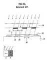
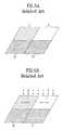
- a reverse rubbing processwill be described with reference to FIG. 1 .
- FIG. 1 aan entire substrate 11 on which a polyimide 12 is deposited is processed by rubbing.
- a mono-domainis formed as shown in FIG. 1 b .
- FIG. 1 cone domain is blocked by a photoresist 13 . Rubbing is then performed in a direction opposite to the rubbing direction of FIG. 1 a .
- FIG. 1 da domain which is not blocked by the photoresist 13 is processed by reverse rubbing.
- FIG. 1 eif the photoresist 13 is removed, a substrate divided into two domains having opposite pretilt angles can be obtained.
- the liquid crystal cell manufactured by the above rubbing processhas problems in that dust or static electricity occurs during the rubbing process, thereby reducing yield or damaging the liquid crystal cell.
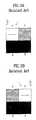
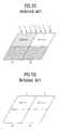
- FIG. 2 aa substrate 21 on which an alignment film 22 is deposited is periodically shielded by a mask 23 having a light-transmitting portion 25 and a light-shielding portion 24 .
- a first pretiltis determined in a portion 26 where light is transmitted.
- the mask 23is rearranged to shield light in the portion 26 .
- a second pretiltis determined in a portion 27 where light is shielded in FIG. 2 a .
- a first substrate of two domains having different pretiltscan be obtained.
- a second substrate of two domainscan be obtained by the above alignment method and lower and upper substrates are assembled with each other.
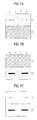
- areas Q and Rare light-shielded, and the photo-alignment methods having an angle ⁇ of irradiation in FIGS. 2 a and 2 b are sequentially applied to areas O and P as shown in FIGS. 3 a and 3 b .
- the areas O and Pare then light-shielded, and the photo-alignment methods having an angle ⁇ of irradiation in FIGS. 2 a and 2 b are sequentially applied to the areas Q and R as shown in FIGS. 3 c and 3 d .
- light irradiation of total four timesis performed on the substrate, thereby obtaining a substrate having four domains.
- the first substrate and the second substrate in which four domains are formedare bonded to face each other and then the liquid crystal is injected thereto, so that a four-domain liquid crystal cell can be obtained.
- a semi-transparent portion 43 of a maskis arranged in some area of a substrate 41 on which an alignment film 42 is deposited, and then light irradiation is performed.
- the irradiated lightis absorbed in the alignment film 42 on the substrate 41 in an aperture portion.
- some of the irradiated lightis only absorbed in the alignment film 42 in an area of the alignment film 42 of the substrate 41 corresponding to the semi-transparent portion 43 of the mask.
- Polysiloxane based materials used as the alignment film 42are characterized in that the size of tie pretilt angle becomes small as absorbing light energy increases. Accordingly, the size of the pretilt angle formed in the alignment film can easily be controlled.
- a substrate having different pretilt angles and divided pixelsis manufactured, and a sectional view of the substrate is shown in FIG. 4 b .
- a liquid crystal cellis manufactured in such a manner that upper and lower substrates are bonded to each, other by applying the substrate of FIG. 4 b .
- alignment direction of each domainis identical in each substrate but the size of the pretilt angle is different. Accordingly, a multi-domain is formed to improve a viewing angle.
- a four domain liquid crystal cellcan be obtained as shown in FIG. 5 . In this case, areas III and IV are light-shielded and the photo-alignment method of FIG.
- the first methodrequires light irradiation of eight times (vertical irradiation of four times and tilt irradiation of four times) into the upper and lower substrates to form a multi-domain divided into two pixel areas, and mask bond no process of four times. Moreover, to form a multi-domain having four domains, the process steps increase two times. Thus, in addition to light irradiation and mask bonding processes of several times, a cap between the masks and the substrate should additionally be controlled. These process steps are unattractive in view of the mass production.
- the second methodrequires light irradiation of four times (vertical irradiation of two times and tilt irradiation of two times) into the upper and lower substrates and mask bonding process of two times when forming a multi-domain having two domains.
- the light irradiation and the mask bonding process stepshave been reduced but error may occur in arranging a number of masks, thereby reducing the productivity.
- the present inventionis directed to a method for manufacturing a multi-domain liquid crystal cell that substantially obviates one or more of the problems due to limitations and disadvantages of the related art.
- An object of the present inventionis to provide a method for manufacturing a multi-domain liquid crystal cell fin which a photo mask required for photo-alignment is improved to perform tilt irradiation having two different directions by irradiation of one time, so that alignment division of a unit pixel can be realized and a multi-domain liquid crystal cell can be obtained by a simple process.
- Another object of the present inventionis to provide a method for manufacturing a multi-domain liquid crystal cell in which the number of masks is reduced to reduce error that may occur in arranging the masks due to control of a gap between the masks and the substrate.
- a method for manufacturing a multi-domain liquid crystal display device having a pixelcomprising the steps of: forming an alignment film on at least one of first and second substrates; covering the alignment film with a mask, the mask including a first surface having a plurality of light-transmitting portions and light-shielding portions and a second surface having light-shielding portions corresponding to the light-transmitting portions of the second surface; irradiating light from an upper portion of the mask; and assembling the first and second substrates.
- FIG. 1shows a process for manufacturing a two-domain liquid crystal cell according to a related art rubbing method
- FIG. 2shows a process for manufacturing a two-domain liquid crystal cell according to a related art photo-alignment method
- FIG. 3shows a process for manufacturing a four-domain liquid crystal cell according to a related art photo-alignment method
- FIG. 4shows a process for manufacturing a two-domain liquid crystal cell according to a related art another photo-alignment method
- FIG. 5shows a process for manufacturing a four-domain liquid crystal cell according to a related art another photo-alignment method
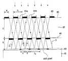
- FIG. 6shows a process for manufacturing a two-domain liquid crystal cell according to a photo-alignment method using a mask of the present invention.
- FIG. 7shows a process for manufacturing a four-domain liquid crystal cell according to a photo-alignment method using a mask of the present invention.
- FIG. 6shows a process for manufacturing a two-domain liquid crustal cell in which a pixel is alignment divided by UV irradiation of one time using a mask.
- an alignment film 62is deposited on a substrate 61 .
- a plurality of firs and second light-transmitting portions 64 a and 64 b and light-shielding portions 63are arranged at constant intervals on a first surface 65 of the substrate 61 on which the alignment film is deposited.
- a mask 67is arranged on a second surface 66 in such a manner that the light-shielding portion is arranged in a position corresponding to the light-transmitting portion of the first surface 65 and the light-transmitting portion is arranged in a position corresponding to the light-shielding portion. Then, UV irradiation is performed using the mask 67 as shown in a tilt solid arrow on a top of FIG. 6 . As shown in FIG. 6, the light irradiated to the first light-transmitting portions 64 a is obliquely irradiated at an angle of ⁇ in a direction of arrow x so that the light is absorbed in a first domain of the alignment film 62 on the substrate 61 .
- the light irradiated to the second light-transmitting portions 64 bis tilt irradiated at an angle of ⁇ in a direction of arrow y so that the light is absorbed in a second domain of the alignment film 62 on the substrate 61 . Accordingly, two different tilt irradiation steps are performed by irradiation of one time to alignment-divide a unit pixel, so that a liquid crystal cell having simply divided domains can be manufactured. At this time, since the size of the pixel is defined as shown in FIG. 5, the following conditions should be satisfied.
- the mask pattern periodis an arrangement period of the light-transmitting portion or the light-shielding portion of the mask
- the pixel pitchis an arrangement period of the pixel
- the mask pattern widthis a width of the light-transmitting portion or light-shielding portion.
- the liquid crystal cellcan be manufactured by applying the photo-alignment method of FIG. 6 to the upper and lower substrates.
- the irradiation anglecan be controlled variously by varying the distance between the first surface and the second surface based on w ⁇ tan ⁇ . If the irradiation angle is varied, the size of the pretilt angle in each domain of the substrate is varied. Accordingly, the viewing angle between neighboring domains is compensated, so that the multi-domain liquid crystal cell can be obtained by the simple process.
- FIG. 7shows a method for forming a four-domain liquid crystal cell by applying the above method. That is, referring to FIG. 7 a , a first area A filled with dots on the substrate on which the alignment film is deposited is covered with the above mask while a second area B filled with oblique lines is covered with an opaque mask.
- the first light irradiation of UVsolid line arrow on a top in the drawing
- a pretiltis formed by the first light irradiation as shown in FIG. 7 a .
- FIG. 7shows a method for forming a four-domain liquid crystal cell by applying the above method. That is, referring to FIG. 7 a , a first area A filled with dots on the substrate on which the alignment film is deposited is covered with the above mask while a second area B filled with oblique lines is covered with an opaque mask.
- the first light irradiation of UVsolid line arrow on a top in the drawing
- a pretiltis formed by the first light
- the left arrow of the first area Adenotes a pretilt direction generated by UV in direction y passed through the second light-transmitting portion 64 b , i.e., UV irradiated at an angle of ⁇
- the right arrow of the first area Adenotes a pretilt direction generated by UV in direction x passed through the first light-transmitting portion 64 a , i.e., UV irradiated at an angle of ⁇ .
- a pretiltis not formed in the second area B of the alignment film corresponding to the opaque portion having optical transmittivity of 0%. However, two domains having different pretilt directions are formed in the area covered with the mask. Next, as shown in FIG.
- the first area A in which the pretilt is determinedis covered with the opaque mask while the second area A is covered with the mask 67 having the distance d′ between the first surface 65 and the second surface 66 .
- the second light irradiation(solid arrow on a top of the drawing) can be performed in the second area B to have a pretilt angle different from that of the first area A.
- a pretiltis formed by the second light irradiation as shown in FIG. 7 b .
- the left arrow of the second area Bdenotes a pretilt direction generated by UV in direction y passed through the second light-transmitting portion 64 b , i.e., UV irradiated at an angle of ⁇
- the right arrow of the second area Bdenotes a pretilt direction generated by UV in direction x passed through the first light-transmitting portion 64 a , i.e., UV irradiated at an angle of ⁇ . Since the second light irradiation is blocked by the mask in the first area A of the alignment film corresponding to the opaque portion having optical transmittivity of 0%, the pretilt formed by the first irradiation remains in the same manner as FIG. 7 a .
- the main liquid crystal cell of FIG. 4can be formed.
- the method for manufacturing a multi-domain liquid crystal cellhas the following advantages.
- the light-transmitting portions and the light-shielding portionsare arranged on the first surface at constant intervals, and the photo-alignment is performed using the mask which is formed in such a manner that the light-shielding portions are arranged in a position corresponding to the light-transmitting portion of the first surface and the light-transmitting portions are arranged in a position corresponding to the light-shielding portion. Accordingly, alignment division of the unit pixel can be realized by irradiation of one time and the number of the manufacturing process steps can be reduced. Furthermore, since alignment division of the pixel is realized by one mask, the steps of arranging a number of masks are reduced. Thus, error that may occur in arranging the masks is reduced, so that reliability of the alignment is improved, thereby improving the productivity and lowering the production cost in case of mass production.
Landscapes
- Physics & Mathematics (AREA)
- Nonlinear Science (AREA)
- Mathematical Physics (AREA)
- Chemical & Material Sciences (AREA)
- Crystallography & Structural Chemistry (AREA)
- General Physics & Mathematics (AREA)
- Optics & Photonics (AREA)
- Spectroscopy & Molecular Physics (AREA)
- Liquid Crystal (AREA)
Abstract
Description
Claims (29)
Priority Applications (1)
| Application Number | Priority Date | Filing Date | Title |
|---|---|---|---|
| US10/197,835US6787292B2 (en) | 1999-10-14 | 2002-07-19 | Method for manufacturing multi-domain liquid crystal cell |
Applications Claiming Priority (2)
| Application Number | Priority Date | Filing Date | Title |
|---|---|---|---|
| KR10-1999-0044621AKR100475107B1 (en) | 1999-10-14 | 1999-10-14 | A method of manufacturing a multi-domain liquid crystal display device |
| KR1999-44621 | 1999-10-14 |
Related Child Applications (1)
| Application Number | Title | Priority Date | Filing Date |
|---|---|---|---|
| US10/197,835ContinuationUS6787292B2 (en) | 1999-10-14 | 2002-07-19 | Method for manufacturing multi-domain liquid crystal cell |
Publications (1)
| Publication Number | Publication Date |
|---|---|
| US6479218B1true US6479218B1 (en) | 2002-11-12 |
Family
ID=19615407
Family Applications (2)
| Application Number | Title | Priority Date | Filing Date |
|---|---|---|---|
| US09/686,815Expired - Fee RelatedUS6479218B1 (en) | 1999-10-14 | 2000-10-12 | Method for manufacturing multi-domain liquid crystal cell |
| US10/197,835Expired - LifetimeUS6787292B2 (en) | 1999-10-14 | 2002-07-19 | Method for manufacturing multi-domain liquid crystal cell |
Family Applications After (1)
| Application Number | Title | Priority Date | Filing Date |
|---|---|---|---|
| US10/197,835Expired - LifetimeUS6787292B2 (en) | 1999-10-14 | 2002-07-19 | Method for manufacturing multi-domain liquid crystal cell |
Country Status (2)
| Country | Link |
|---|---|
| US (2) | US6479218B1 (en) |
| KR (1) | KR100475107B1 (en) |
Cited By (6)
| Publication number | Priority date | Publication date | Assignee | Title |
|---|---|---|---|---|
| US20030059724A1 (en)* | 1999-10-14 | 2003-03-27 | Choi Young Seok | Method for manufacturing multi-domain liquid crystal cell |
| US20040246419A1 (en)* | 2002-07-31 | 2004-12-09 | International Business Machines Corporation | Apparatus and method for forming alignment layer |
| US20060227272A1 (en)* | 2001-08-01 | 2006-10-12 | Hideo Chida | Liquid crystal display device treated by UV irradiation |
| US20110027494A1 (en)* | 2007-07-03 | 2011-02-03 | Kim Leong Tan | Non-etched flat polarization-selective diffractive optical elements |
| US10845520B2 (en)* | 2014-04-03 | 2020-11-24 | Rolic Ag | Optical devices with patterned anisotropy incorporating parallax optic |
| CN112904619A (en)* | 2021-01-27 | 2021-06-04 | 福州大学 | LCD optical alignment method for double-domain alignment |
Families Citing this family (13)
| Publication number | Priority date | Publication date | Assignee | Title |
|---|---|---|---|---|
| KR100845410B1 (en)* | 2003-05-14 | 2008-07-10 | 엘지디스플레이 주식회사 | Multi Domain Alignment Film Formation Method |
| KR100845714B1 (en)* | 2003-12-30 | 2008-07-10 | 엘지디스플레이 주식회사 | Multi-domain liquid crystal display and manufacturing method |
| JP4549819B2 (en)* | 2004-11-12 | 2010-09-22 | シャープ株式会社 | Liquid crystal display device and manufacturing method thereof |
| KR100911459B1 (en) | 2008-08-06 | 2009-08-11 | 삼성전자주식회사 | Alignment film forming method, manufacturing method of liquid crystal display device and alignment film forming device using same |
| KR100923052B1 (en)* | 2008-08-06 | 2009-10-22 | 삼성전자주식회사 | Oriented substrate |
| KR20100071141A (en)* | 2008-12-19 | 2010-06-29 | 삼성전자주식회사 | Display substrate, liquid crystal display device having the display substrate and method of manufacturing the display substrate |
| KR101710694B1 (en) | 2010-08-10 | 2017-02-28 | 삼성디스플레이 주식회사 | Mask for photoalignment, mathod for photoalignment and liquid crystal display |
| TW201239483A (en)* | 2011-03-25 | 2012-10-01 | Chimei Innolux Corp | Methods for manufacturing LCD substrates and LCDs |
| KR101782013B1 (en) | 2011-06-03 | 2017-10-24 | 삼성디스플레이 주식회사 | Exposure device and manufacturing method of liquid crystal display |
| CN108873597A (en)* | 2018-06-26 | 2018-11-23 | 南京中电熊猫液晶显示科技有限公司 | A kind of mask plate and orientation exposure method |
| CN112904621B (en)* | 2021-01-27 | 2023-12-29 | 福州大学 | Light alignment light path system of liquid crystal display tri-domain alignment layer |
| CN112904620A (en)* | 2021-01-27 | 2021-06-04 | 福州大学 | Double-domain optical alignment LCD light path system |
| CN112904622B (en)* | 2021-01-27 | 2022-08-12 | 福州大学 | A kind of photo-alignment method of liquid crystal display three-domain alignment layer |
Citations (76)
| Publication number | Priority date | Publication date | Assignee | Title |
|---|---|---|---|---|
| US3912920A (en) | 1974-02-06 | 1975-10-14 | Josuke Kubota | Polarized light illumination device |
| EP0261712A1 (en) | 1986-09-04 | 1988-03-30 | Koninklijke Philips Electronics N.V. | Picture display cell, method of forming an orientation layer on a substrate of the picture display cell and monomeric compounds for use in the orientation layer |
| JPS6460833A (en) | 1987-08-31 | 1989-03-07 | Agency Ind Science Techn | Optical recording element |
| JPH01251344A (en) | 1988-03-30 | 1989-10-06 | Agency Of Ind Science & Technol | Optical recording element |
| JPH01251345A (en) | 1988-03-30 | 1989-10-06 | Agency Of Ind Science & Technol | Optical recording element |
| JPH0255330A (en) | 1988-08-22 | 1990-02-23 | Matsushita Electric Ind Co Ltd | Manufacturing method of alignment film for liquid crystal |
| US4974941A (en) | 1989-03-08 | 1990-12-04 | Hercules Incorporated | Process of aligning and realigning liquid crystal media |
| JPH02298917A (en) | 1989-05-12 | 1990-12-11 | Agency Of Ind Science & Technol | Optical element |
| JPH0336527A (en) | 1989-07-03 | 1991-02-18 | Agency Of Ind Science & Technol | Optical element |
| JPH03120503A (en) | 1989-10-04 | 1991-05-22 | Matsushita Electric Ind Co Ltd | Polarizing component |
| JPH03241311A (en) | 1990-02-20 | 1991-10-28 | Seiko Epson Corp | Polarized light source device |
| US5073294A (en) | 1990-03-07 | 1991-12-17 | Hercules Incorporated | Process of preparing compositions having multiple oriented mesogens |
| JPH047520A (en) | 1990-04-25 | 1992-01-10 | Agency Of Ind Science & Technol | Method for orienting liquid crystal by linearly polarized light |
| JPH04284421A (en) | 1991-03-13 | 1992-10-09 | Agency Of Ind Science & Technol | Liquid crystal orientation method by diagonal light |
| JPH04350822A (en) | 1991-05-29 | 1992-12-04 | Nec Corp | Liquid crystal oriented film and production thereof and liquid crystal optical element |
| JPH0519208A (en) | 1991-07-10 | 1993-01-29 | Nec Corp | Polarization beam splitter array |
| EP0525478A2 (en) | 1991-07-26 | 1993-02-03 | F. Hoffmann-La Roche Ag | Liquid crystal display cell |
| EP0525473A2 (en) | 1991-07-26 | 1993-02-03 | F. Hoffmann-La Roche Ag | Display device with liquid crystal cell |
| JPH0534699A (en) | 1991-07-29 | 1993-02-12 | Toshiba Corp | Liquid crystal display element |
| JPH0553513A (en) | 1991-08-26 | 1993-03-05 | Toshiba Corp | Production of liquid crystal oriented film |
| EP0549283A2 (en) | 1991-12-20 | 1993-06-30 | Fujitsu Limited | Domain divided liquid crystal display device |
| WO1994001754A1 (en) | 1992-07-03 | 1994-01-20 | Norsk Hydro A.S | Method for analyzing gas in liquid media and equipment for carrying out the method |
| EP0611786A1 (en) | 1993-02-17 | 1994-08-24 | F. Hoffmann-La Roche Ag | Orientation layer for liquid crystals |
| EP0635748A1 (en) | 1993-07-23 | 1995-01-25 | Sharp Kabushiki Kaisha | Liquid crystal display apparatus and method for producing the same |
| US5389698A (en) | 1991-07-26 | 1995-02-14 | Hoffmann-La Roche Inc. | Process for making photopolymers having varying molecular orientation using light to orient and polymerize |
| JPH0756173A (en) | 1993-08-17 | 1995-03-03 | Stanley Electric Co Ltd | Liquid crystal display device, liquid crystal alignment treatment method, and liquid crystal display device manufacturing method |
| GB2281977A (en) | 1993-09-18 | 1995-03-22 | Gold Star Co | Orientation film for a liquid crystal display |
| WO1995018189A1 (en) | 1993-12-30 | 1995-07-06 | Barrett Boating Canvas & Upholstery, Inc. | Method for adhering a flexible sheet to a semi-rigid thermoplastic resinous sheet |
| WO1995022075A1 (en) | 1994-02-09 | 1995-08-17 | The Secretary Of State For Defence | Liquid crystal device alignment |
| US5447662A (en) | 1990-12-21 | 1995-09-05 | Hoffmann-La Roche Inc. | Optically non-linear polymeric coatings |
| US5453862A (en) | 1992-09-04 | 1995-09-26 | Stanley Electric Co., Ltd. | Rubbing-free (chiral) nematic liquid crystal display |
| JPH07261185A (en) | 1994-03-24 | 1995-10-13 | Stanley Electric Co Ltd | Liquid crystal display element manufacturing method |
| JPH07318861A (en) | 1994-05-19 | 1995-12-08 | Canon Inc | Plate-shaped polarizing element, polarized illumination device using the plate-shaped polarizing element, and projector using the plate-shaped polarizing element |
| JPH07318942A (en) | 1994-05-27 | 1995-12-08 | Sharp Corp | Liquid crystal display device, manufacturing method thereof and manufacturing device thereof |
| DE4420585A1 (en) | 1994-06-13 | 1995-12-14 | Merck Patent Gmbh | Electro-optical system |
| US5479282A (en) | 1993-02-10 | 1995-12-26 | Stanley Electric Co., Ltd. | Liquid crystal display of multi-domain structure |
| EP0708354A1 (en) | 1994-10-14 | 1996-04-24 | International Business Machines Corporation | Liquid crystal display device and method of manufacture |
| US5538823A (en) | 1993-05-20 | 1996-07-23 | Goldstar Co., Ltd. | Liquid crystal device utilizing thermostable polymeric material |
| WO1996022561A1 (en) | 1995-01-20 | 1996-07-25 | Geo-Centers, Inc. | Liquid crystal composition and alignment layer |
| EP0742471A2 (en) | 1995-05-10 | 1996-11-13 | Stanley Electric Co., Ltd. | Arrangement for rubbingless orientation of liquid crystals with tilt |
| US5576862A (en) | 1993-06-29 | 1996-11-19 | Stanley Electric Co., Ltd. | Positive orientations of liquid crystal molecules in a multi-domain liquid crystal display cell |
| JPH08334790A (en) | 1995-06-07 | 1996-12-17 | Fujitsu Ltd | Liquid crystal display panel and manufacturing method thereof |
| EP0750212A2 (en) | 1995-06-22 | 1996-12-27 | International Business Machines Corporation | Liquid crystal display device |
| US5602601A (en) | 1995-04-21 | 1997-02-11 | L. G. Electronics Inc. | Phase error corrector for HDTV reception system |
| US5627667A (en) | 1993-01-29 | 1997-05-06 | Sharp Kabushiki Kaisha | Liquid crystal display apparatus, a method for producing the same, and a substrate |
| EP0788012A2 (en) | 1996-02-05 | 1997-08-06 | Stanley Electric Co., Ltd. | Homeotropic orientation liquid crystal display and its manufacture |
| GB2309794A (en) | 1996-02-01 | 1997-08-06 | Lg Electronics Inc | Alignment layers for liquid crystal devices |
| GB2309793A (en) | 1996-01-09 | 1997-08-06 | Lg Electronics Inc | Controlling pretilt angle direction in a liquid crystal cell |
| US5657105A (en) | 1994-01-10 | 1997-08-12 | Honeywell Inc. | Multi-domain liquid crystal displays |
| GB2310048A (en) | 1995-12-29 | 1997-08-13 | Lg Electronics Inc | Alignment layers for liquid crystal cells |
| JPH09265095A (en) | 1996-03-27 | 1997-10-07 | Matsushita Electric Ind Co Ltd | Method for producing alignment film of liquid crystal molecules |
| JPH09318946A (en) | 1996-05-27 | 1997-12-12 | Stanley Electric Co Ltd | Liquid crystal display element manufacturing method |
| US5705096A (en) | 1995-03-15 | 1998-01-06 | Alps Electric Co., Ltd. | UV crosslinking compound, alignment film for LCD component and LCD component |
| US5712696A (en) | 1994-02-17 | 1998-01-27 | Stanley Electric, Co., Ltd. | Manufacture of LCD device by transferring the orientation state from a parent substrate to a child substrate |
| JPH1078584A (en)* | 1996-07-29 | 1998-03-24 | Lg Electron Inc | Production of multidomain liquid crystal cell |
| GB2317964A (en) | 1996-10-07 | 1998-04-08 | Lg Electronics Inc | Controlling the pretilt of a liquid crystal cell |
| JPH1090684A (en) | 1996-09-12 | 1998-04-10 | Ushio Inc | Polarized light irradiation device for photo-alignment of alignment film of liquid crystal display device |
| US5739833A (en)* | 1994-06-23 | 1998-04-14 | Brother Kogyo Kabushiki Kaisha | Jet printing ink and printing method using the ink |
| GB2319093A (en) | 1996-11-07 | 1998-05-13 | Lg Electronics Inc | Fabricating a liquid crystal cell |
| JPH10154658A (en) | 1996-09-27 | 1998-06-09 | Ushio Inc | Proximity exposure system with variable irradiation angle |
| JPH10161126A (en) | 1996-12-03 | 1998-06-19 | Ran Technical Service Kk | Method for forming oriented film and exposing device |
| US5786041A (en) | 1995-06-07 | 1998-07-28 | International Business Machines Corporation | Alignment film, a method for producing the alignment film and a liquid crystal display device using the alignment film |
| US5824377A (en) | 1995-11-20 | 1998-10-20 | Lg Electronics Inc. | Photosensitive material for orientation of liquid crystal device and liquid crystal device thereof |
| JPH10332932A (en) | 1997-05-30 | 1998-12-18 | Ushio Inc | Filter that polarizes light in a specific wavelength range |
| US5856430A (en) | 1996-03-29 | 1999-01-05 | Alliant Techsystems Inc. | Process and materials for inducing pre-tilt in liquid crystals and liquid crystal displays |
| WO1999008148A2 (en) | 1997-08-05 | 1999-02-18 | Elsicon, Inc. | Optical exposure systems and processes for alignment of liquid crystals |
| US5880803A (en) | 1995-11-06 | 1999-03-09 | Sharp Kabushiki Kaisha | Liquid crystal display element with a portion of an alignment layer covers spacer is directly bonded to the alignment layer on the other substrate |
| US5882238A (en) | 1995-12-08 | 1999-03-16 | Lg Electronics Inc. | Method for manufacturing bend-aligned liquid crystal cell using light |
| US5909265A (en)* | 1996-09-20 | 1999-06-01 | Lg Electronics Inc. | Method of fabricating a multi-domain liquid crystal cell |
| JPH11194345A (en) | 1997-10-29 | 1999-07-21 | Ushio Inc | Polarized light irradiation device for photo-alignment of alignment film of liquid crystal display device |
| JPH11194344A (en) | 1997-10-29 | 1999-07-21 | Ushio Inc | Polarized light irradiation device for photo-alignment of alignment film of liquid crystal display device |
| US5928561A (en) | 1995-09-29 | 1999-07-27 | The Secretary Of State For Defence In Her Britannic Majesty's Government Of The United Kingdom Of Great Britain And Northern Ireland | Polymers for liquid crystal alignment |
| US5963448A (en) | 1997-06-18 | 1999-10-05 | Allen-Bradley Company, Llc | Industrial controller having redundancy and using connected messaging and connection identifiers to enable rapid switchover without requiring new connections to be opened or closed at switchover |
| US5982466A (en) | 1996-11-29 | 1999-11-09 | Lg Electronics Inc | Method of forming an alignment layer and a liquid crystal cell having same using patterning by light irradiation |
| JP3120503B2 (en) | 1991-10-18 | 2000-12-25 | 山陽特殊製鋼株式会社 | Method for producing anisotropic powder |
| JP3241311B2 (en) | 1997-10-23 | 2001-12-25 | 佐賀工業株式会社 | Concrete pouring device |
Family Cites Families (5)
| Publication number | Priority date | Publication date | Assignee | Title |
|---|---|---|---|---|
| JP2527243Y2 (en) | 1993-09-21 | 1997-02-26 | 株式会社ナカニシオプティカル | Eyeglass Temple Joint Structure |
| US6124914A (en)* | 1996-05-10 | 2000-09-26 | International Business Machines Corporation | Method an apparatus for forming an alignment pattern on a surface using a particle beam useful for a liquid crystal |
| US5739883A (en)* | 1996-08-30 | 1998-04-14 | Nan Ya Technology Corporation | Manufacturing method and structure for aligner of liquid crystal display |
| KR19980047849A (en)* | 1996-12-16 | 1998-09-15 | 이우복 | Polarizer patterned with multi-domain and manufacturing method thereof |
| KR100475107B1 (en)* | 1999-10-14 | 2005-03-09 | 엘지.필립스 엘시디 주식회사 | A method of manufacturing a multi-domain liquid crystal display device |
- 1999
- 1999-10-14KRKR10-1999-0044621Apatent/KR100475107B1/ennot_activeExpired - Fee Related
- 2000
- 2000-10-12USUS09/686,815patent/US6479218B1/ennot_activeExpired - Fee Related
- 2002
- 2002-07-19USUS10/197,835patent/US6787292B2/ennot_activeExpired - Lifetime
Patent Citations (96)
| Publication number | Priority date | Publication date | Assignee | Title |
|---|---|---|---|---|
| US3912920A (en) | 1974-02-06 | 1975-10-14 | Josuke Kubota | Polarized light illumination device |
| EP0261712A1 (en) | 1986-09-04 | 1988-03-30 | Koninklijke Philips Electronics N.V. | Picture display cell, method of forming an orientation layer on a substrate of the picture display cell and monomeric compounds for use in the orientation layer |
| JPS6460833A (en) | 1987-08-31 | 1989-03-07 | Agency Ind Science Techn | Optical recording element |
| JPH01251344A (en) | 1988-03-30 | 1989-10-06 | Agency Of Ind Science & Technol | Optical recording element |
| JPH01251345A (en) | 1988-03-30 | 1989-10-06 | Agency Of Ind Science & Technol | Optical recording element |
| JPH0255330A (en) | 1988-08-22 | 1990-02-23 | Matsushita Electric Ind Co Ltd | Manufacturing method of alignment film for liquid crystal |
| US5032009A (en) | 1989-03-08 | 1991-07-16 | Hercules Incorporated | Process of aligning and realigning liquid crystal media |
| US4974941A (en) | 1989-03-08 | 1990-12-04 | Hercules Incorporated | Process of aligning and realigning liquid crystal media |
| JPH02298917A (en) | 1989-05-12 | 1990-12-11 | Agency Of Ind Science & Technol | Optical element |
| US5296321A (en) | 1989-07-03 | 1994-03-22 | Agency Of Industrial Science & Technology | Photorecording element, method for production thereof, and the liquid crystal cell comprising the same |
| JPH0336527A (en) | 1989-07-03 | 1991-02-18 | Agency Of Ind Science & Technol | Optical element |
| JPH03120503A (en) | 1989-10-04 | 1991-05-22 | Matsushita Electric Ind Co Ltd | Polarizing component |
| JPH03241311A (en) | 1990-02-20 | 1991-10-28 | Seiko Epson Corp | Polarized light source device |
| US5073294A (en) | 1990-03-07 | 1991-12-17 | Hercules Incorporated | Process of preparing compositions having multiple oriented mesogens |
| JPH047520A (en) | 1990-04-25 | 1992-01-10 | Agency Of Ind Science & Technol | Method for orienting liquid crystal by linearly polarized light |
| US5447662A (en) | 1990-12-21 | 1995-09-05 | Hoffmann-La Roche Inc. | Optically non-linear polymeric coatings |
| JPH04284421A (en) | 1991-03-13 | 1992-10-09 | Agency Of Ind Science & Technol | Liquid crystal orientation method by diagonal light |
| JPH04350822A (en) | 1991-05-29 | 1992-12-04 | Nec Corp | Liquid crystal oriented film and production thereof and liquid crystal optical element |
| JPH0519208A (en) | 1991-07-10 | 1993-01-29 | Nec Corp | Polarization beam splitter array |
| JPH05232473A (en) | 1991-07-26 | 1993-09-10 | F Hoffmann La Roche Ag | Liquid crystal display cell |
| EP0525473A2 (en) | 1991-07-26 | 1993-02-03 | F. Hoffmann-La Roche Ag | Display device with liquid crystal cell |
| EP0525478A2 (en) | 1991-07-26 | 1993-02-03 | F. Hoffmann-La Roche Ag | Liquid crystal display cell |
| US5784139A (en) | 1991-07-26 | 1998-07-21 | Rolic Ag | Image display device |
| US5389698A (en) | 1991-07-26 | 1995-02-14 | Hoffmann-La Roche Inc. | Process for making photopolymers having varying molecular orientation using light to orient and polymerize |
| JPH0534699A (en) | 1991-07-29 | 1993-02-12 | Toshiba Corp | Liquid crystal display element |
| JPH0553513A (en) | 1991-08-26 | 1993-03-05 | Toshiba Corp | Production of liquid crystal oriented film |
| JP3120503B2 (en) | 1991-10-18 | 2000-12-25 | 山陽特殊製鋼株式会社 | Method for producing anisotropic powder |
| EP0549283A2 (en) | 1991-12-20 | 1993-06-30 | Fujitsu Limited | Domain divided liquid crystal display device |
| WO1994001754A1 (en) | 1992-07-03 | 1994-01-20 | Norsk Hydro A.S | Method for analyzing gas in liquid media and equipment for carrying out the method |
| US5453862A (en) | 1992-09-04 | 1995-09-26 | Stanley Electric Co., Ltd. | Rubbing-free (chiral) nematic liquid crystal display |
| US5627667A (en) | 1993-01-29 | 1997-05-06 | Sharp Kabushiki Kaisha | Liquid crystal display apparatus, a method for producing the same, and a substrate |
| US5657102A (en) | 1993-01-29 | 1997-08-12 | Sharp Kabushiki Kaisha | Liquid crystal display apparatus, a method for producing the same, and a substrate having an alignment layer with different degrees of roughness |
| US5479282A (en) | 1993-02-10 | 1995-12-26 | Stanley Electric Co., Ltd. | Liquid crystal display of multi-domain structure |
| EP0611786A1 (en) | 1993-02-17 | 1994-08-24 | F. Hoffmann-La Roche Ag | Orientation layer for liquid crystals |
| US5539074A (en) | 1993-02-17 | 1996-07-23 | Hoffmann-La Roche Inc. | Linear and cyclic polymers or oligomers having a photoreactive ethene group |
| US5538823A (en) | 1993-05-20 | 1996-07-23 | Goldstar Co., Ltd. | Liquid crystal device utilizing thermostable polymeric material |
| US5576862A (en) | 1993-06-29 | 1996-11-19 | Stanley Electric Co., Ltd. | Positive orientations of liquid crystal molecules in a multi-domain liquid crystal display cell |
| EP0635748A1 (en) | 1993-07-23 | 1995-01-25 | Sharp Kabushiki Kaisha | Liquid crystal display apparatus and method for producing the same |
| JPH0756173A (en) | 1993-08-17 | 1995-03-03 | Stanley Electric Co Ltd | Liquid crystal display device, liquid crystal alignment treatment method, and liquid crystal display device manufacturing method |
| US5767994A (en) | 1993-09-18 | 1998-06-16 | Goldstar Co., Ltd. | Orientation film of photopolymer in a liquid crystal display and a method of forming the film |
| US5464669A (en) | 1993-09-18 | 1995-11-07 | Goldstar Co., Ltd. | Method for forming an orientation film of photopolymer in a liquid crystal display |
| GB2281977A (en) | 1993-09-18 | 1995-03-22 | Gold Star Co | Orientation film for a liquid crystal display |
| WO1995018189A1 (en) | 1993-12-30 | 1995-07-06 | Barrett Boating Canvas & Upholstery, Inc. | Method for adhering a flexible sheet to a semi-rigid thermoplastic resinous sheet |
| US5657105A (en) | 1994-01-10 | 1997-08-12 | Honeywell Inc. | Multi-domain liquid crystal displays |
| GB2286893A (en) | 1994-02-09 | 1995-08-30 | Secr Defence | Liquid crystal alignment |
| WO1995022075A1 (en) | 1994-02-09 | 1995-08-17 | The Secretary Of State For Defence | Liquid crystal device alignment |
| US5712696A (en) | 1994-02-17 | 1998-01-27 | Stanley Electric, Co., Ltd. | Manufacture of LCD device by transferring the orientation state from a parent substrate to a child substrate |
| JPH07261185A (en) | 1994-03-24 | 1995-10-13 | Stanley Electric Co Ltd | Liquid crystal display element manufacturing method |
| JPH07318861A (en) | 1994-05-19 | 1995-12-08 | Canon Inc | Plate-shaped polarizing element, polarized illumination device using the plate-shaped polarizing element, and projector using the plate-shaped polarizing element |
| US5604615A (en) | 1994-05-27 | 1997-02-18 | Sharp Kabushiki Kaisha | Liquid crystal display device and methods for producing same with alignment layer having new bond formation or bond cleavage reaction of molecular chains by light irradiation |
| JPH07318942A (en) | 1994-05-27 | 1995-12-08 | Sharp Corp | Liquid crystal display device, manufacturing method thereof and manufacturing device thereof |
| WO1995034843A1 (en) | 1994-06-13 | 1995-12-21 | Merck Patent Gmbh | Electro-optical system |
| DE4420585A1 (en) | 1994-06-13 | 1995-12-14 | Merck Patent Gmbh | Electro-optical system |
| US5739833A (en)* | 1994-06-23 | 1998-04-14 | Brother Kogyo Kabushiki Kaisha | Jet printing ink and printing method using the ink |
| EP0708354A1 (en) | 1994-10-14 | 1996-04-24 | International Business Machines Corporation | Liquid crystal display device and method of manufacture |
| US5764326A (en) | 1994-10-14 | 1998-06-09 | International Business Machines Corporation | Multiple direction rotatable liquid crystal display device and a method for its manufacture |
| US5578351A (en) | 1995-01-20 | 1996-11-26 | Geo-Centers, Inc. | Liquid crystal composition and alignment layer |
| WO1996022561A1 (en) | 1995-01-20 | 1996-07-25 | Geo-Centers, Inc. | Liquid crystal composition and alignment layer |
| US5705096A (en) | 1995-03-15 | 1998-01-06 | Alps Electric Co., Ltd. | UV crosslinking compound, alignment film for LCD component and LCD component |
| US5602601A (en) | 1995-04-21 | 1997-02-11 | L. G. Electronics Inc. | Phase error corrector for HDTV reception system |
| EP0742471A2 (en) | 1995-05-10 | 1996-11-13 | Stanley Electric Co., Ltd. | Arrangement for rubbingless orientation of liquid crystals with tilt |
| US5786041A (en) | 1995-06-07 | 1998-07-28 | International Business Machines Corporation | Alignment film, a method for producing the alignment film and a liquid crystal display device using the alignment film |
| JPH08334790A (en) | 1995-06-07 | 1996-12-17 | Fujitsu Ltd | Liquid crystal display panel and manufacturing method thereof |
| EP0750212A2 (en) | 1995-06-22 | 1996-12-27 | International Business Machines Corporation | Liquid crystal display device |
| US5928561A (en) | 1995-09-29 | 1999-07-27 | The Secretary Of State For Defence In Her Britannic Majesty's Government Of The United Kingdom Of Great Britain And Northern Ireland | Polymers for liquid crystal alignment |
| US5880803A (en) | 1995-11-06 | 1999-03-09 | Sharp Kabushiki Kaisha | Liquid crystal display element with a portion of an alignment layer covers spacer is directly bonded to the alignment layer on the other substrate |
| US5824377A (en) | 1995-11-20 | 1998-10-20 | Lg Electronics Inc. | Photosensitive material for orientation of liquid crystal device and liquid crystal device thereof |
| US5882238A (en) | 1995-12-08 | 1999-03-16 | Lg Electronics Inc. | Method for manufacturing bend-aligned liquid crystal cell using light |
| US5859682A (en) | 1995-12-29 | 1999-01-12 | Lg Electronics Inc. | Method for manufacturing liquid crystal cell using light |
| GB2310048A (en) | 1995-12-29 | 1997-08-13 | Lg Electronics Inc | Alignment layers for liquid crystal cells |
| GB2309793A (en) | 1996-01-09 | 1997-08-06 | Lg Electronics Inc | Controlling pretilt angle direction in a liquid crystal cell |
| US5889571A (en) | 1996-02-01 | 1999-03-30 | Lg Electronics Inc. | Ultraviolet irradiating device for photo-alignment process and an irradiating method using the same |
| JPH09211465A (en) | 1996-02-01 | 1997-08-15 | Lg Electron Inc | Light irradiation device for light alignment and light irradiation method |
| DE19703682A1 (en) | 1996-02-01 | 1997-08-07 | Lg Electronics Inc | UV light irradiation apparatus for photo alignment processes and irradiation processes using the same |
| GB2309794A (en) | 1996-02-01 | 1997-08-06 | Lg Electronics Inc | Alignment layers for liquid crystal devices |
| EP0788012A2 (en) | 1996-02-05 | 1997-08-06 | Stanley Electric Co., Ltd. | Homeotropic orientation liquid crystal display and its manufacture |
| JPH09211468A (en) | 1996-02-05 | 1997-08-15 | Stanley Electric Co Ltd | Liquid crystal display device manufacturing method and liquid crystal display device |
| JPH09265095A (en) | 1996-03-27 | 1997-10-07 | Matsushita Electric Ind Co Ltd | Method for producing alignment film of liquid crystal molecules |
| US5856430A (en) | 1996-03-29 | 1999-01-05 | Alliant Techsystems Inc. | Process and materials for inducing pre-tilt in liquid crystals and liquid crystal displays |
| US5856431A (en) | 1996-03-29 | 1999-01-05 | Alliant Techsystems Inc. | Process and materials for inducing pre-tilt in liquid crystals and liquid crystal displays |
| JPH09318946A (en) | 1996-05-27 | 1997-12-12 | Stanley Electric Co Ltd | Liquid crystal display element manufacturing method |
| US5853818A (en) | 1996-07-29 | 1998-12-29 | Lg Electronics, Inc. | Method for manufacturing multi-domain liquid crystal cell |
| JPH1078584A (en)* | 1996-07-29 | 1998-03-24 | Lg Electron Inc | Production of multidomain liquid crystal cell |
| JPH1090684A (en) | 1996-09-12 | 1998-04-10 | Ushio Inc | Polarized light irradiation device for photo-alignment of alignment film of liquid crystal display device |
| US5909265A (en)* | 1996-09-20 | 1999-06-01 | Lg Electronics Inc. | Method of fabricating a multi-domain liquid crystal cell |
| JPH10154658A (en) | 1996-09-27 | 1998-06-09 | Ushio Inc | Proximity exposure system with variable irradiation angle |
| GB2317964A (en) | 1996-10-07 | 1998-04-08 | Lg Electronics Inc | Controlling the pretilt of a liquid crystal cell |
| GB2319093A (en) | 1996-11-07 | 1998-05-13 | Lg Electronics Inc | Fabricating a liquid crystal cell |
| US5982466A (en) | 1996-11-29 | 1999-11-09 | Lg Electronics Inc | Method of forming an alignment layer and a liquid crystal cell having same using patterning by light irradiation |
| JPH10161126A (en) | 1996-12-03 | 1998-06-19 | Ran Technical Service Kk | Method for forming oriented film and exposing device |
| JPH10332932A (en) | 1997-05-30 | 1998-12-18 | Ushio Inc | Filter that polarizes light in a specific wavelength range |
| US5963448A (en) | 1997-06-18 | 1999-10-05 | Allen-Bradley Company, Llc | Industrial controller having redundancy and using connected messaging and connection identifiers to enable rapid switchover without requiring new connections to be opened or closed at switchover |
| WO1999008148A2 (en) | 1997-08-05 | 1999-02-18 | Elsicon, Inc. | Optical exposure systems and processes for alignment of liquid crystals |
| JP3241311B2 (en) | 1997-10-23 | 2001-12-25 | 佐賀工業株式会社 | Concrete pouring device |
| JPH11194344A (en) | 1997-10-29 | 1999-07-21 | Ushio Inc | Polarized light irradiation device for photo-alignment of alignment film of liquid crystal display device |
| JPH11194345A (en) | 1997-10-29 | 1999-07-21 | Ushio Inc | Polarized light irradiation device for photo-alignment of alignment film of liquid crystal display device |
Non-Patent Citations (30)
| Title |
|---|
| A. Lien et al.; "UV Modification of Surface Pretilt of Alignment Layers..."; Appl. Phys. Lett. 67 (21) pp. 3108-3110,1598 (Nov. 1995). |
| A. Lien et al.; "UV-Type Two-Domain Wide Viewing Angle..."; Asia Display '95; pp. 593-596. |
| D. S. Seo et al.; "Surface Alignment of Liquid Crystals in LCDs..."; SID 93 Digest; pp. 954-956. |
| F. Yamada et al., "A New Photo-Alignment Scheme for LC-Cell Pretilt...", SID 97 Digest; pp. 715-718. |
| Gibbons, "Nature" (Letters toNature); vol. 351; pp. 49-50; May 2, 1991. |
| H.S. Soh et al.; "The Realization of Wide Viewing Angle..."; Euro Display '96; pp. 579-582. |
| Hasegawa et al., "Nematic Homogeneous Photo Alignment By Polyimide Exposure to Linearly Polarized UV," J. of Photopolymer Science and Technology, vol. 8, No. 2, pp. 241-248, 1995. |
| J. Chen et al.; "Mechanism of Liquid Crystal Alignment..." SID 96 Digest, pp. 634-637. |
| J. Chen et al.; "Model of Liquid Crystal Alignment..."; The American Physical Society; vol. 54 No. 2; pp. 1599-1603 (Aug. 1996). |
| J. H. Kim et al.; "Late-News Poster: Photo-Alignment of Liquid Crystals"; SID '96 Digest; pp. 646-647, 649. |
| J.L. West; "Polarized UV-Exposed Polyimide Films for Liquid-Crystal Alignment..."; SID 95 Digest; pp. 703-705. |
| Jpn. J. Appl. Phys., "Molecular Orientations and Optical Transmission Properties of Liquid Crystal Cells with Slit-Patterned Electrodes," vol. 36 (1997) 1178-1184. |
| K. W. Lee et al.; "Late-News Poster: Mechanism of UV Modification..."; SID 96 Digest; pp. 638-641. |
| K. Y. Han et al.; "A Study on the Photo-Alignment of the Polymer-Containing..."; SID 97 Digest, pp. 707-710. |
| Kunihiro Ichimura; "Nematic Liquid Crystal Alignment"; MCLC; pp. 998-1001, 1044; Oct.1993. |
| M. Schadt et al.; "Optical Patterning of Multidomain LCDs..."; SID 97 Digest; pp. 397-400. |
| M. Schadt et al.; Optical Patterning of Multi-domain...; Nature vol. 381, pp. 212-215 (May 1996). |
| M. Schadt; "Investigation of the Mechanism of the Surface-Induced Alignment..."; SID 95 Digest; pp. 528-531. |
| M.S. Nam et al., "Wide-Viewing-Angle TFT-LCD..."; SID 97 Digest; pp. 933-936. |
| R. Shashidhar et al.; "A New Non-Rubbing Technique..."; SID 97 Digest; pp. 315-318. |
| Schadt et al., "Surface-Induced Parallel Alignment of Liquid Crystals"; Jpn. J. Appl. Phys. vol. 31; pp. 2155-2164; Jul. 1992. |
| Shannon et al., "Patterned Optical Properties in Photopolymerized Surface-Aligned Liquid-Crystal Films," Nature, vol. 368, pp. 532-533, 1994. |
| T. Hashimoto; "TN-LCD with Quartered Subpixels Using Polarized..."; SID 95 Digest; pp. 877-800. |
| T. Saitoh et al.; "A New Hybrid N-TB Mode LCD..." Asia Display '95; pp. 589-592. |
| T. Sugiyama et al.; "Electro-Optic Characteristics of Amorphous..."; SID 94 Digest; pp. 915-918. |
| T. Yamamoto et al.; "Liquid Crystal Alignment..."; SID 96 Digest; pp. 642-645 with 2 Cover Pages. |
| Y. Iimura; "Prospects of the Photo-Alignment Technique..."; SID 97 Digest; pp. 311-314. |
| Y. Saitoh et al.; "Stability of UV-Type Two-Domain Wide-Viewing-Angle..."; SID 96 Digest; pp. 662-665. |
| Y. Toko et al.; "TN-LCDs Fabricated by Non-Rubbing Showing Wide..."; SID 93 Digest; pp. 622-625. |
| Yasufami Iimura et al.; "Alignment Control of a Liquid Crystal..."; Jpn. J. Appl. Phys.; vol. 32; pp. 93-96 (Jan.1993). |
Cited By (22)
| Publication number | Priority date | Publication date | Assignee | Title |
|---|---|---|---|---|
| US20030059724A1 (en)* | 1999-10-14 | 2003-03-27 | Choi Young Seok | Method for manufacturing multi-domain liquid crystal cell |
| US6787292B2 (en)* | 1999-10-14 | 2004-09-07 | Lg.Philips Lcd Co., Ltd. | Method for manufacturing multi-domain liquid crystal cell |
| US20080291388A1 (en)* | 2001-08-01 | 2008-11-27 | Sharp Kabushiki Kaisha | Liquid crystal display device treated by uv irradiation |
| US7782430B2 (en) | 2001-08-01 | 2010-08-24 | Sharp Kabushiki Kaisha | Liquid crystal display device treated by UV irradiation |
| US8681300B2 (en) | 2001-08-01 | 2014-03-25 | Sharp Kabushiki Kaisha | Liquid crystal display device treated by UV irradiation |
| US20060227272A1 (en)* | 2001-08-01 | 2006-10-12 | Hideo Chida | Liquid crystal display device treated by UV irradiation |
| US7251001B2 (en)* | 2001-08-01 | 2007-07-31 | Sharp Kabushiki Kaisha | Liquid crystal display device treated by UV irradiation |
| US20070285606A1 (en)* | 2001-08-01 | 2007-12-13 | Hideo Chida | Liquid crystal display device treated by UV irradiation |
| US8400595B2 (en) | 2001-08-01 | 2013-03-19 | Sharp Kabushiki Kaisha | Liquid crystal display device treated by UV irradiation |
| US7430033B2 (en) | 2001-08-01 | 2008-09-30 | Sharp Kabushiki Kaisha | Liquid crystal display device treated by UV irradiation |
| US8085373B2 (en) | 2001-08-01 | 2011-12-27 | Sharp Kabushiki Kaisha | Liquid crystal display device treated by UV irradiation |
| US20110187974A1 (en)* | 2001-08-01 | 2011-08-04 | Sharp Kabushiki Kaisha | Liquid crystal display device treated by uv irradiation |
| US7944532B2 (en) | 2001-08-01 | 2011-05-17 | Sharp Kabushiki Kaisha | Liquid crystal display device treated by UV irradiation |
| US7057692B2 (en)* | 2002-07-31 | 2006-06-06 | International Business Machines Corporation | Apparatus and method for forming alignment layer with mask having a curved or warped surface |
| US20040246419A1 (en)* | 2002-07-31 | 2004-12-09 | International Business Machines Corporation | Apparatus and method for forming alignment layer |
| US7400376B2 (en) | 2002-07-31 | 2008-07-15 | International Business Machines Corporation | Apparatus and method for forming alignment layer |
| US20060132689A1 (en)* | 2002-07-31 | 2006-06-22 | International Business Machines Corporation | Apparatus and method for forming alignment layer |
| US20110027494A1 (en)* | 2007-07-03 | 2011-02-03 | Kim Leong Tan | Non-etched flat polarization-selective diffractive optical elements |
| US8643822B2 (en)* | 2007-07-03 | 2014-02-04 | Jds Uniphase Corporation | Non-etched flat polarization-selective diffractive optical elements |
| US10845520B2 (en)* | 2014-04-03 | 2020-11-24 | Rolic Ag | Optical devices with patterned anisotropy incorporating parallax optic |
| EP3126883B1 (en)* | 2014-04-03 | 2023-07-12 | ROLIC Technologies AG | Optical devices with patterned anisotropy incorporating parallax optic |
| CN112904619A (en)* | 2021-01-27 | 2021-06-04 | 福州大学 | LCD optical alignment method for double-domain alignment |
Also Published As
| Publication number | Publication date |
|---|---|
| KR100475107B1 (en) | 2005-03-09 |
| KR20010037225A (en) | 2001-05-07 |
| US20030059724A1 (en) | 2003-03-27 |
| US6787292B2 (en) | 2004-09-07 |
Similar Documents
| Publication | Publication Date | Title |
|---|---|---|
| US6479218B1 (en) | Method for manufacturing multi-domain liquid crystal cell | |
| KR100191787B1 (en) | Method for manufacturing a liquid crystal cell having a wide viewing angle | |
| KR100923052B1 (en) | Oriented substrate | |
| JPH09197408A (en) | Method for producing twisted nematic liquid crystal cell using light | |
| JP2008097049A (en) | Liquid crystal display device and manufacturing method thereof | |
| KR100257976B1 (en) | An in-plane switching mode liquid crystal display device | |
| KR100831278B1 (en) | Multi Domain Liquid Crystal Display | |
| KR20110014912A (en) | Liquid Crystal Display and Manufacturing Method Thereof | |
| US9841636B2 (en) | Liquid crystal display device | |
| JP5086458B2 (en) | Liquid crystal display device and manufacturing method thereof | |
| US7067224B2 (en) | Method for fabricating a liquid crystal display device | |
| JP2003270653A (en) | Liquid crystal display device and method of manufacturing the same | |
| KR100293431B1 (en) | In-plane switching mode liquid crystal display device | |
| KR0182415B1 (en) | Manufacturing method of substrate for liquid crystal display | |
| KR100244537B1 (en) | A liquid crystal display device | |
| KR100244730B1 (en) | A method for fabricating liquid crystal display device | |
| JPH07333634A (en) | Liquid crystal display panel | |
| US20030142254A1 (en) | Reflective liquid crystal display and method for fabricating the same | |
| KR101041090B1 (en) | Manufacturing method of alignment substrate and liquid crystal display device having same | |
| JP5292594B2 (en) | LCD panel | |
| US6822714B1 (en) | Liquid crystal display element and method for manufacturing it | |
| US6762817B2 (en) | Liquid crystal display device having improved structure of injection opening | |
| KR100255433B1 (en) | Liquid crystal display panel | |
| KR100815915B1 (en) | LCD and its manufacturing method | |
| KR101494738B1 (en) | Liquid crystal display panel and method of manufacturing the same |
Legal Events
| Date | Code | Title | Description |
|---|---|---|---|
| AS | Assignment | Owner name:LG. PHILIPS LCD CO., LTD., KOREA, REPUBLIC OF Free format text:ASSIGNMENT OF ASSIGNORS INTEREST;ASSIGNOR:CHOI, YOUNG SEOK;REEL/FRAME:011212/0286 Effective date:20001010 | |
| AS | Assignment | Owner name:L. G. PHILIPS LCD CO., LTD., KOREA, REPUBLIC OF Free format text:ASSIGNMENT OF ASSIGNORS INTEREST;ASSIGNOR:CHOI, YOUNG SEOK;REEL/FRAME:011518/0410 Effective date:20010116 | |
| FPAY | Fee payment | Year of fee payment:4 | |
| AS | Assignment | Owner name:LG DISPLAY CO., LTD., KOREA, REPUBLIC OF Free format text:CHANGE OF NAME;ASSIGNOR:LG.PHILIPS LCD CO., LTD.;REEL/FRAME:021754/0230 Effective date:20080304 Owner name:LG DISPLAY CO., LTD.,KOREA, REPUBLIC OF Free format text:CHANGE OF NAME;ASSIGNOR:LG.PHILIPS LCD CO., LTD.;REEL/FRAME:021754/0230 Effective date:20080304 | |
| FEPP | Fee payment procedure | Free format text:PAYOR NUMBER ASSIGNED (ORIGINAL EVENT CODE: ASPN); ENTITY STATUS OF PATENT OWNER: LARGE ENTITY Free format text:PAYER NUMBER DE-ASSIGNED (ORIGINAL EVENT CODE: RMPN); ENTITY STATUS OF PATENT OWNER: LARGE ENTITY | |
| FPAY | Fee payment | Year of fee payment:8 | |
| REMI | Maintenance fee reminder mailed | ||
| LAPS | Lapse for failure to pay maintenance fees | ||
| STCH | Information on status: patent discontinuation | Free format text:PATENT EXPIRED DUE TO NONPAYMENT OF MAINTENANCE FEES UNDER 37 CFR 1.362 | |
| FP | Lapsed due to failure to pay maintenance fee | Effective date:20141112 |