US6478931B1 - Apparatus and method for intra-layer modulation of the material deposition and assist beam and the multilayer structure produced therefrom - Google Patents
Apparatus and method for intra-layer modulation of the material deposition and assist beam and the multilayer structure produced therefromDownload PDFInfo
- Publication number
- US6478931B1 US6478931B1US09/634,457US63445700AUS6478931B1US 6478931 B1US6478931 B1US 6478931B1US 63445700 AUS63445700 AUS 63445700AUS 6478931 B1US6478931 B1US 6478931B1
- Authority
- US
- United States
- Prior art keywords
- monolayers
- incident
- energy
- layer
- adatom
- Prior art date
- Legal status (The legal status is an assumption and is not a legal conclusion. Google has not performed a legal analysis and makes no representation as to the accuracy of the status listed.)
- Expired - Fee Related, expires
Links
Images


Classifications
- C—CHEMISTRY; METALLURGY
- C23—COATING METALLIC MATERIAL; COATING MATERIAL WITH METALLIC MATERIAL; CHEMICAL SURFACE TREATMENT; DIFFUSION TREATMENT OF METALLIC MATERIAL; COATING BY VACUUM EVAPORATION, BY SPUTTERING, BY ION IMPLANTATION OR BY CHEMICAL VAPOUR DEPOSITION, IN GENERAL; INHIBITING CORROSION OF METALLIC MATERIAL OR INCRUSTATION IN GENERAL
- C23C—COATING METALLIC MATERIAL; COATING MATERIAL WITH METALLIC MATERIAL; SURFACE TREATMENT OF METALLIC MATERIAL BY DIFFUSION INTO THE SURFACE, BY CHEMICAL CONVERSION OR SUBSTITUTION; COATING BY VACUUM EVAPORATION, BY SPUTTERING, BY ION IMPLANTATION OR BY CHEMICAL VAPOUR DEPOSITION, IN GENERAL
- C23C14/00—Coating by vacuum evaporation, by sputtering or by ion implantation of the coating forming material
- C23C14/22—Coating by vacuum evaporation, by sputtering or by ion implantation of the coating forming material characterised by the process of coating
- C23C14/54—Controlling or regulating the coating process
- C—CHEMISTRY; METALLURGY
- C23—COATING METALLIC MATERIAL; COATING MATERIAL WITH METALLIC MATERIAL; CHEMICAL SURFACE TREATMENT; DIFFUSION TREATMENT OF METALLIC MATERIAL; COATING BY VACUUM EVAPORATION, BY SPUTTERING, BY ION IMPLANTATION OR BY CHEMICAL VAPOUR DEPOSITION, IN GENERAL; INHIBITING CORROSION OF METALLIC MATERIAL OR INCRUSTATION IN GENERAL
- C23C—COATING METALLIC MATERIAL; COATING MATERIAL WITH METALLIC MATERIAL; SURFACE TREATMENT OF METALLIC MATERIAL BY DIFFUSION INTO THE SURFACE, BY CHEMICAL CONVERSION OR SUBSTITUTION; COATING BY VACUUM EVAPORATION, BY SPUTTERING, BY ION IMPLANTATION OR BY CHEMICAL VAPOUR DEPOSITION, IN GENERAL
- C23C14/00—Coating by vacuum evaporation, by sputtering or by ion implantation of the coating forming material
- C23C14/06—Coating by vacuum evaporation, by sputtering or by ion implantation of the coating forming material characterised by the coating material
- C23C14/14—Metallic material, boron or silicon
- C23C14/16—Metallic material, boron or silicon on metallic substrates or on substrates of boron or silicon
- C23C14/165—Metallic material, boron or silicon on metallic substrates or on substrates of boron or silicon by cathodic sputtering
- C—CHEMISTRY; METALLURGY
- C23—COATING METALLIC MATERIAL; COATING MATERIAL WITH METALLIC MATERIAL; CHEMICAL SURFACE TREATMENT; DIFFUSION TREATMENT OF METALLIC MATERIAL; COATING BY VACUUM EVAPORATION, BY SPUTTERING, BY ION IMPLANTATION OR BY CHEMICAL VAPOUR DEPOSITION, IN GENERAL; INHIBITING CORROSION OF METALLIC MATERIAL OR INCRUSTATION IN GENERAL
- C23C—COATING METALLIC MATERIAL; COATING MATERIAL WITH METALLIC MATERIAL; SURFACE TREATMENT OF METALLIC MATERIAL BY DIFFUSION INTO THE SURFACE, BY CHEMICAL CONVERSION OR SUBSTITUTION; COATING BY VACUUM EVAPORATION, BY SPUTTERING, BY ION IMPLANTATION OR BY CHEMICAL VAPOUR DEPOSITION, IN GENERAL
- C23C14/00—Coating by vacuum evaporation, by sputtering or by ion implantation of the coating forming material
- C23C14/22—Coating by vacuum evaporation, by sputtering or by ion implantation of the coating forming material characterised by the process of coating
- C23C14/34—Sputtering
- C23C14/46—Sputtering by ion beam produced by an external ion source
Definitions
- the present inventionis directed to the fabrication of multilayer structures, and more particularly an improved physical-vapor deposition apparatus and method of use (and structure produced therefrom) for intra-layer modulated material deposition and assist beam.
- plasma sputtering depositionare characterized by crossed electric and magnetic fields in an evacuated chamber into which an inert, ionizable gas, such as argon, is introduced.
- the gasis ionized by electrons accelerated by the electric field, which forms a plasma in proximity to a target structure.
- the crossed electric and magnetic fieldsconfine the electrons in a zone between the target and substrate structures.
- the gas ionsstrike the target structure, causing ejection of atoms that are incident on a workpiece, typically a substrate on which it is desired to deposit one or more layers of selected target materials.
- IBDion beam deposition
- the use of a lower background pressureresults in less scattering of sputtered particles during the transit from the target to the substrate;
- control of the ion beam directionalityprovides a variable angle of incidence of the beam at the target;
- a nearly monoenergetic beam having a narrow energy distributionprovides control of the sputter yield and deposition process as a function of ion energy and enables accurate beam focusing and scanning;
- the ion beamis independent of target and substrate processes which allows changes in target and substrate materials and geometry while maintaining constant beam characteristics and allowing independent control of the beam energy and current density;
- a second inert gas ion beamcan be directed at the substrate to provide ion assisted deposition.
- MBEmolecular beam epitaxy
- GMRgiant magneto-resistive
- MRAMmagnetic random access memory
- GMR materialsusually consisting of at least two magnetic nanostructure entities separated by a nonmagnetic spacer. They display a large change of resistance upon the application of a magnetic field. GMR materials have a larger relative resistance change and have increased field sensitivity as compared against traditional anisotropic magneto-resistive or MR materials, such as Ni80Fe20 films.
- the improved relative resistance change and field sensitivity of GMR materials and related magnetic sensing elementsallow the production of sensors having greater sensitivity and signal-to-noise ratio than conventional sensors. Thus, for instance, data storage systems using GMR read sensors can read data in smaller bit areas as compared to conventional read head devices.
- material stacks for fabricating GMR sensorsgenerally use 6 to 8 layers of 4 to 6 different materials, as compared to the MR material stacks, which usually have only 3 layers of materials such as permalloy layers with Soft Adjacent Layers (SAL).
- SALSoft Adjacent Layers
- Spin-valve GMR read headsare comprised of multi-layer depositions of 10 to 100 angstrom thick material films having precise thickness and microstructure control as well as extremely cohesive interface control at each interface of a multi-layer spin-valve GMR stack.
- Each spin-valve GMR stackmust have good crystalinity in conjunction with abrupt and smooth material interfaces with minimal interface mixing to ensure proper GMR response and to establish excellent thermal stability.
- GMR stacksmay require controlled deposition of metallic multilayers which comprise ultrathin films as thin as about 5 to 10 atomic monolayers.
- MRAMmagnetic random access memories
- MRAM devicesare monolithic silicon-based nonvolatile memory devices presently based on a hysteretic effect in magneto-resistive or MR materials.
- MRAM devicesare beginning to be used in aerospace and military applications due to their excellent nonvolatile memory bit retention and radiation hardness behavior.
- the MRAM devicescan be easily integrated with silicon integrated circuits for embedded memory in a host of future applications in cell phones, personal computers, microprocessors, personal digital assistants (PDAs), etc.
- PDAspersonal digital assistants
- the implementation of GMR materialssuch as spin-dependent tunnel junctions, could improve the electrical performance of MRAM devices to make MRAM devices competitive with semiconductor DRAM and flash EPROM memory devices.
- the performance of MRAM memorydepends on precise control of layer thickness values and the microstructures of various thin films in a GMR stack of thin metallic films. Thickness fluctuations and other interface or microstructural variations in thin metallic layers can cause variation in MRAM device performance.
- GMR materialshave significant technological importance because they can be used to develop highly sensitive magnetic field sensors, read heads for disk drives, and MRAM that promise nonvolatility, radiation hardness, low power consumption, densities comparable to dynamic random access memory and access speeds comparable to static random access memory. All these applications require a high GMR ratio (defined as the maximum resistance change divided by the resistance at magnetic saturation), a low saturation magnetic field, a near-zero coercivity, a weak temperature dependence, and a high thermal stability. Many groups are now seeking to develop a vapor phase synthesis process that results in multilayers with this optimum combination of properties.
- GMR propertiesare sensitive to nanoscale structural features of the films, their defect populations and the intrinsic properties of the material system. For instance, the lowest resistance appears to result from a sandwich structure with chemically separated planar interfaces.
- the GMR ratiotherefore depends on nanoscale features of the multilayers such as the wavelength and amplitude of the interfacial roughness and the width and extent of interfacial chemical mixing. It may also be affected by grain texture, composition, layer purity, and the various types of lattice defects (including vacancies, voids, dis-locations, and twins) trapped in the films.
- U.S. Pat. No. 5,661,449 to Araki et al.discloses forming a multilayer film of a plurality of magnetic and non-magentic layers alternatively stacked.
- the '449 patentdiscloses forming the plurality of layers ( 104 , 105 , 106 ) with a deposition energy of 0.01 to 10.0 eV.
- the approach of the '449 patentis unsatisfactory because it fails to account for the modulation required within each individual layer at the atomic monolayer application so as to provide for reduced interfacial roughness and layer intermixing as in the present invention.
- FIGS. 1A and 1Billustrate the result of a conventional physical-vapor deposition process whereby the deposition energy is held constant during the deposition of each individual layer ( 104 , 105 , 106 ).
- a multilayer structure 100having been deposited on a nickel substrate 101 , having a growth direction in the y-coordinate direction.
- the orientation of the multilayer structure 100 and substrate 101is defined by letting the x, y, and z coordinates correspond to the reference numbers 112 , 111 , and 110 , respectively.
- the substrate crystalconsisted of 120 (224) planes in the x direction, 3 (111) planes in the y direction, and 16 (220) planes in the z direction. To prevent the crystal from shifting during adatom impact and minimize the effect of the bottom surface, the bottom two (111) planes were fixed.
- the multilayer structure 100was deposited by alternatively depositing about 20 ⁇ (approximately 10 monolayers) of copper (Cu) followed by about 20 ⁇ (approximately 10 monolayers) of nickel (Ni).
- thermal evaporatione.g., MBE
- high pressuree.g., diode
- the multilayer structure 100when the multilayer structure 100 was deposited with an incident energy at 5.0 eV the interfacial roughness of both the copper on nickel interface 103 and the nickel on copper interface 102 were significantly reduced. However, the multilayer structure 100 suffers from excessive layer intermixing as the copper atoms are dispersed in the subsequently deposited nickel layer.
- FIGS. 2A and 2Bother types of defects, including vacancies, twins, and dislocations are prevalent in conventional approaches. Typical examples of twin and dislocation structures are depicted in FIGS. 2A and 2B, respectively.
- the present inventionhas numerous applications including, but not limited thereto, for the growth of metal multilayers (e.g., magneto-electronic devices for sensing magnetic fields, magnetic random access memory, spin transistors and the like), semiconductor heterostructures including magnetic semiconductors, ceramic multilayers, optical filters or mirrors, x-ray mirrors, laser mirrors (with dielectric and metal multilayers), laser diodes, fiber optic waveguides and combinations of these material systems.
- metal multilayerse.g., magneto-electronic devices for sensing magnetic fields, magnetic random access memory, spin transistors and the like
- semiconductor heterostructuresincluding magnetic semiconductors, ceramic multilayers, optical filters or mirrors, x-ray mirrors, laser mirrors (with dielectric and metal multilayers), laser diodes, fiber optic waveguides and combinations of these material systems.
- the present invention systems, devices, and structureswill have a broad application including computers, peripheral computer components, cameras, telephones, televisions, miscellaneous electronic and communication components, and personal digital assistants (PDAs).
- PDAspersonal digital assistants
- a method of producing a multilayer structure by using a physical-vapor deposition apparatuscomprises the steps of: forming a bottom layer having a first material wherein a first plurality of monolayers of the first material is deposited on an underlayer using a low incident adatom energy. Next, a second plurality of monolayers of the first material is deposited on top of the first plurality of monolayers of the first material using a high incident adatom energy. Thereafter, the method further includes forming a second layer having a second material wherein a first plurality of monolayers of the second material is deposited on the second plurality of monolayers of the first material using a low incident adatom energy. Next, a second plurality of monolayers of the second material is deposited on the first plurality of monolayers of the second material using a high incident adatom energy.
- the incident energycan be ramped with the thickness of a given layer as the monolayers are accumulated/deposited.
- the second monolayerhas energy less than the third monolayer but more than the first monolayer, i.e., E n ⁇ 1 ⁇ E n ⁇ E n+1 .
- Some of the advantages of the present inventionare that it provides an apparatus and method for fabricating multilayer structures that has reduced interfacial roughness and interlayer mixing.
- FIG. 1Ais a schematic drawing of atomic configurations of conventional Ni/Cu/Ni multilayers deposited with single incident adatom energy of 0.1 eV throughout the entire layer.
- FIG. 1Bis a schematic drawing of atomic configurations of conventional Ni/Cu/Ni multilayers deposited with single incident adatom energy of 5.0 eV throughout the entire layer.
- FIG. 2Ais a schematic drawing of Ni/Cu/Ni multilayers in a single (220) plane showing twins defects.
- FIG. 2Bis a schematic drawing of Ni/Cu/Ni multilayers in a pair of (220) planes showing dislocations.
- FIG. 3is a block diagram illustrating a preferred embodiment of an ion beam deposition (IBD) system according to the principles of the present invention.
- IBDion beam deposition
- FIG. 4is a graphical representation showing the parameters used to compute roughness(r 1 )
- FIG. 5is an atomic configurations of Ni/Cu/Ni multilayers deposited using intra-layer modulated incident energy according to the principles of the present invention.
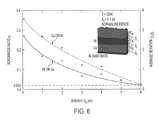
- FIG. 6is a graphical representation showing the interfacial roughness as a function of energy E h for intra-layer modulated energy deposition according to the principles of the present invention.
- FIG. 7is a graphical representation showing the interfacial mixing of copper in the nickel layer as a function of energy E h for intra-layer modulated energy deposition according to the principles of the present invention.
- FIG. 3a detailed diagram illustrating a preferred embodiment of an ion beam (sputtering) deposition (IBD) system 180 according to the principles of the present invention is shown, as similarly illustrated in U.S. Pat. No. 5,492,605 to Pinarbasi.
- the ion beam deposition (IBD) system 180includes a vacuum chamber 181 in which a primary ion beam source 183 is mounted, a multi-target, rotatable support 185 having one or more targets 187 of selected materials mounted thereon and a deposition substrate, underlayer, or workpiece 189 .
- the underlayer 189may be considered a buffer layer made of material including, for example, Ta, Nb, Mo, Ti, W, Cr, or the like, and/or alloys thereof.
- An ion beam provided by the primary ion beam source 183is directed at a selected target 191 where the impacting ions cause sputtering of the target material.
- the sputtered atoms emitted by the target materialare directed onto the deposition substrate, underlayer, or other workpiece 189 on which is formed a layer of the selected target 191 material.
- a thickness monitor 193is positioned closely adjacent the underlayer 189 to provide real-time, in-situ monitoring of the thickness of the growing film during deposition.
- the underlayer, substrate or other workpiece 189is mounted on a movable (or non-movable) pedestal or support member 195 which is retrieved into a cart mounted load-lockstage (loading port) 197 via a gate valve 199 for changing the workpiece 189 .
- a turbo pump 147is provided to pump down the load-lockstage 197 .
- the pedestal 195is temperature controlled, i.e., heated and cooled as required for the particular deposition process.
- the pedestal 195may be rotatable by means of a linear/rotary motor drive (not shown) to allow selective deposition and other operations on a number of substrates 189 without reload between operations.
- the pedestal 195includes a shutter 196 to prevent bombardment of the substrate 189 by sputtered materials during pre- and post-deposition operations such as, for example, precleaning of the target 191 with the primary ion source 183 .
- Moveable shields 194are provided to prevent material buildup on portions of the pedestal 195 and the gate valve 199 components.
- shutter 196 or equivalent shutter meansare incorporated so as to control the adatom incident energy during the intra layer deposition, i.e., at the atomic monolayer scale.
- Alternative emobodiments of modulating the adatom incident energywill discussed later.
- the vacuum chamber 181is maintained at an internal operation pressure on the order of 1 ⁇ 10 ⁇ 4 Torr by a cart mounted vacuum pump system 141 via a port provided in the chamber adjacent rear door 143 .
- Hinged front and rear doors 142 and 143respectively, provide access to the chamber and components mounted therein for cleaning, replacement of targets and adjustment or repair.
- a number of observation ports 145 and accessory ports 149are provided in the chamber walls.
- Internal electric heaters 144 mounted within the chamberprovide a controlled environment within the chamber. Power and instrumentation for the system and its components are provided by a power supply/instrumentation module 121 coupled to the system via cables 122 .
- the operation of the systemis controlled by a programmable controller 125 or the like coupled to the system via cables 128 .
- the primary ion sourcecomprises an ion gun, such as a Kaufman type ion source or the equivalent, adjustably mounted to provide a variable angle of incidence of the ion beam on the target 191 over a range of 0 degrees, i.e., normal to the target, to about 60 degrees.
- a number of gases including Ar, Kr and Xe gasesare stored in pressurized bottles (not shown) and are selectably ported to the ion source 183 via inlet port 151 to provide a selectable sputtering gas as desired for matching to the selected target material.
- a probe 153(a Faraday Cup is suitable for this purpose) is provided for analysis of the ion beam energy.
- a residual gas analyzer mounted on inside wall of the rear door 143monitors and records partial pressures of the sputtering and background gases continuously, i.e., before, during and after the deposition process.
- the Kaufman source 181provides an ion beam in the energy range of approximately 200 to 2000 eV.
- the ion source voltages, ion beam energy and current, selection of sputtering gas and other ion source parametersare automatically controlled by the programmable controller 125 .
- the controller 125includes a computer 126 coupled to operator input means such as a keyboard means 127 and display means 129 for entry of system operations parameters and instructions.
- a secondary ion gun source 131which may comprise a Kaufman type source or the equivalent, is mounted within the vacuum chamber 181 to provide substrate preclean etch and substrate ion-assisted deposition functions.
- the secondary source 131is mounted to provide an ion beam of desired energy at an angle of incidence nominally at approximately 60 degrees. The angle of incidence is adjustable over a large range (0 to 90 degrees) to provide an optimum angle of incidence as required.
- the secondary ion source 131is ported to a selected gas supply (not shown) via inlet port 135 to provide a desired ionizable gas for the ion source operation.
- the secondary ion source 131is controlled by programmable controller 125 in a manner similar to that of the primary ion source 183 .
- r 1an interfacial roughness parameter (“r 1 ”).
- h il and h irare respectively the height measured from the left and right of the ith asperity, and w i is the width of this asperity. Summation is conducted over the n asperities in the x direction.
- FIG. 5there is shown an illustrative mulitlayer structure formed by the present invention apparatus and method having reduced interfacial roughness and layer intermixing by modulating the incident adatom energy at the atomic monolayer level, i.e., intra-layer modulation by adjusting the incident energy within each layer.
- An exemplary monolayeris depicted by reference number 107 .
- the present invention apparatusdeposits the first few (or predetermined plurality) monolayers 108 of a new metal with a low incident adatom energy level so as to avoid the exchange mechanism with the adjacent existing different layer material. Once, coverage by 4-5 monolayers has been achieved, the subsequent deposition of the energetic atoms needed to flatten the layer is much less likely to cause intermixing.
- a thickness sensor based on electron, ion, or electromagnetic scatteringcan monitor this.
- This low incident adatom energy(about 0.01 to 3.0 eV) avoids the intermixing by the exchange mechanism upon impact.
- the incident energyis then increased during the remaining (or predetermined plurality) monolayers 109 thereby providing a high incident adatom energy levels(about 3.0 eV to 15 eV) to promote the surface flatness without inducing intermixing between different metals of the different layers. It can be seen that interfacial roughness can then be reduced without causing the rise of intermixing.
- the incident energycan be ramped with the thickness of a given layer as the monolayers are accumulated/deposited.
- the second monolayerhas energy less than the third monolayer but more than the first monolayer, i.e., E n ⁇ 1 ⁇ E n ⁇ E n+1 .
- various preselected monolayers and combinations thereofcan be subjected to ramping and ramping variations.
- the low incident adatom energywill range from about 0.1 eV to about 5.0 eV and the high incident adatom energy will vary from about 1.0 eV to about 15.0 eV.
- the energy levelis adapted to fluctuate within these ranges during the process of depositing each layer so as to provide a range of modulated energy within the given layer.
- these rangescould be expanded or restricted when required.
- the present invention intra-layer energy modulation strategyprovides a significant improvement in both the interfacial roughness and the degree of intermixing.
- FIGS. 6 and 7to illustrate the improved characteristics of a multistructure fabrication using the present invention method, the roughness of both interfaces and the degree of copper mixing in the nickel layer were calculated as a function of the high incident adatom energy “E h ”, are illustrated graphically. Because the exchange mechanism is more difficult on flat surfaces, increasing E h not only improves the interfacial smoothness, but it also reduces the mixing. Referring to FIG. 6 it can be seen that the interfacial roughness ratio r l is about 0.025.
- the multilayer structureis subject to only about 1 monolayer or less of interfacial mixing.
- only one monolayer of copperis dispersed (migrated or mixed) with the Nickel layer, and/or vice versa.
- the graphindicates that by virtue of the present invention method the probability of “ ⁇ ” of Cu with at least 8 Ni neighbors is reduced to about 0.002.
- the intra-layer modulated energy deposition method of the present inventionthat uses low incident energies to deposit the first few monolayers of each new metal layer and higher energies for the remainder monolayers results in superior interfacial roughness and interfacial mixing qualities compared to the prior art.
- the present inventioncan be employed for various multilayer structures including, for example, synthesizing GMR multilayers.
- the present inventioncan be implemented by varying the incident kinetic energy of the sputter ions in an ion beam deposition process, controlling the acceleration voltage of the ion beam gun of the inert gas ions bombarding at the target, varying the target-substance distance, as well as varying the background pressure.
- the variation or intra-layer modulation of the incident energymay be done manually or automatically by modifying known automated deposition equipment.
- the shutter 196may be used in conjunction with or substituted by other modulating means, systems, or devices.
- other modulating meansmay include, but not limited thereto, the following (1) electrical, mechanical, manual, or pneumatically operated shutters (2) electrical chopping of the energy or particles (3) filament ignition of the plasma when the target is aligned or deposition is timely (4) DC or RF power source (or alternatively, a pulsed DC or pulsed RF source) applying either continuous wave or pulsed electrical energy (5) power distribution in pulses of varying length to provide time for atoms to diffuse over the deposition surface (6) gating ion beam, atoms, or particles (7) varying angle of incidence (8) electrostatic manipulation of the plasma, ions, or atoms (9) varying temperature (10) and/or equivalents thereof.
- a second preferred alternative embodiment of the present inventionis provided to improve the interfacial roughness and interlayer mixing by using a intra-layer modulating assist ion beam as previously discussed, but with an alternative design.
- the present invention deposition apparatuscan employ a single energy strategy for the primary ion beam source coupled with an intra-layer modulating assist ion beam for bombarding the substrate surface during/after the material is deposited, wherein the energy of the assist ion beam is modulated or varied at the atomic monolayer, with the given layer.
- the second preferred embodiment of the present inventionrelates to the use of an assisting flux of particles (atoms, ions or molecules) for assisting the atomic assembly of multilayers. More specifically it claims the use of low (0-50 eV) translational energy particle fluxes applied continuously or intermittently during/after the atomic deposition of thin films.
- the low energy inert gas ion/atomimpacts with a deposition surface causing the growth surface to flatten without causing intermixing of dissimilar layers.
- the assisting particlesare of similar (or greater) atomic weight to that of the layers constituent atoms, the optimum particle energies for flattening without incurring mixing are in the 1-10 eV range or approximately thereto.
- particle fluxes with controllable low energies and appropriate fluxesinclude, but not limited thereto, the use of molecular beams formed by seeded rarefied supersonic expansions, ionization of a background gas followed by electrostatic acceleration toward the substrate, and ion beam irradiation. All can be designed to provide assisting particle beams with the desired flux and energy to enable growth of multilayer structures with minimal interfacial roughness and intermixing.
- a third preferred alternative embodiment of the present inventionis to combine the modulation strategy together for both the primary ion beam source and the assist beam.
- An advantage of the present inventionis that it provides an apparatus and method for fabricating multilayer structures, using a physical-vapor deposition process, that has reduced interfacial roughness and interlayer mixing.
Landscapes
- Chemical & Material Sciences (AREA)
- Chemical Kinetics & Catalysis (AREA)
- Engineering & Computer Science (AREA)
- Materials Engineering (AREA)
- Mechanical Engineering (AREA)
- Metallurgy (AREA)
- Organic Chemistry (AREA)
- Physical Vapour Deposition (AREA)
Abstract
Description
| Krauss et al. - U.S. Pat. No. 4,923,585 | Pinarbasi - U.S. Pat. No. 5,492,605 |
| Daughton - U.S. Pat. No. 5,569,544 | Daughton - U.S. Pat. No. 5,595,830 |
| Peter - U.S. Pat. No. 5,618,575 | Araki et al. - U.S. Pat. No. 5,661,449 |
| Pinarbasi - U.S. Pat. No. 5,871,622 | Araki et al. - U.S. Pat. No. 5,923,504 |
| Fremgen, Jr. et al. - U.S. Pat. No. 5,982,101 | Daughton - U.S. Pat. No. 5,617,071 |
| Chambliss et al. - U.S. Pat. No. 5,858,455 | Colombo - U.S. Pat. No. 5,951,767 |
| Poole - U.S. Pat. No. 5,976,263 | Chambliss et al. - U.S. Pat. No. 6,015,632 |
| Koike et al. - U.S. Pat. No. 5,795,663 | Moslehi - U.S. Pat. No. 6,051,113 |
| Kamiguchi et al. - U.S. Pat. No. 6,052,262 | Pinarbasi - U.S. Pat. No. 6,063,244 |
| Ngan et al. - U.S. Pat. No. 6,059,872 | Pinarbasi - U.S. Pat. No. 6,086,727 |

Claims (34)
Priority Applications (2)
| Application Number | Priority Date | Filing Date | Title |
|---|---|---|---|
| US09/634,457US6478931B1 (en) | 1999-08-06 | 2000-08-07 | Apparatus and method for intra-layer modulation of the material deposition and assist beam and the multilayer structure produced therefrom |
| US10/246,018US20030054133A1 (en) | 2000-08-07 | 2002-09-18 | Apparatus and method for intra-layer modulation of the material deposition and assist beam and the multilayer structure produced therefrom |
Applications Claiming Priority (3)
| Application Number | Priority Date | Filing Date | Title |
|---|---|---|---|
| US14773399P | 1999-08-06 | 1999-08-06 | |
| US20343900P | 2000-05-10 | 2000-05-10 | |
| US09/634,457US6478931B1 (en) | 1999-08-06 | 2000-08-07 | Apparatus and method for intra-layer modulation of the material deposition and assist beam and the multilayer structure produced therefrom |
Related Child Applications (1)
| Application Number | Title | Priority Date | Filing Date |
|---|---|---|---|
| US10/246,018DivisionUS20030054133A1 (en) | 2000-08-07 | 2002-09-18 | Apparatus and method for intra-layer modulation of the material deposition and assist beam and the multilayer structure produced therefrom |
Publications (1)
| Publication Number | Publication Date |
|---|---|
| US6478931B1true US6478931B1 (en) | 2002-11-12 |
Family
ID=27386593
Family Applications (1)
| Application Number | Title | Priority Date | Filing Date |
|---|---|---|---|
| US09/634,457Expired - Fee RelatedUS6478931B1 (en) | 1999-08-06 | 2000-08-07 | Apparatus and method for intra-layer modulation of the material deposition and assist beam and the multilayer structure produced therefrom |
Country Status (1)
| Country | Link |
|---|---|
| US (1) | US6478931B1 (en) |
Cited By (38)
| Publication number | Priority date | Publication date | Assignee | Title |
|---|---|---|---|---|
| US20020076837A1 (en)* | 2000-11-30 | 2002-06-20 | Juha Hujanen | Thin films for magnetic device |
| US20030224620A1 (en)* | 2002-05-31 | 2003-12-04 | Kools Jacques C.S. | Method and apparatus for smoothing surfaces on an atomic scale |
| US20040005753A1 (en)* | 2000-05-15 | 2004-01-08 | Juhana Kostamo | Method of growing electrical conductors |
| US6759081B2 (en) | 2001-05-11 | 2004-07-06 | Asm International, N.V. | Method of depositing thin films for magnetic heads |
| US20040211672A1 (en)* | 2000-12-20 | 2004-10-28 | Osamu Ishigami | Composite plating film and a process for forming the same |
| US20040255856A1 (en)* | 2001-10-08 | 2004-12-23 | Markus Schumacher | Method and device for depositing a plurality of layers on a substrate |
| US20050000444A1 (en)* | 2001-09-10 | 2005-01-06 | Hass Derek D | Method and apparatus application of metallic alloy coatings |
| US20050093039A1 (en)* | 2003-10-31 | 2005-05-05 | International Business Machines Corporation | Techniques for coupling in semiconductor devices |
| US20050167261A1 (en)* | 2004-01-30 | 2005-08-04 | Deutchman Arnold H. | Treatment process for improving the mechanical, catalytic, chemical, and biological activity of surfaces and articles treated therewith |
| US6946394B2 (en)* | 2000-09-20 | 2005-09-20 | Kla-Tencor Technologies | Methods and systems for determining a characteristic of a layer formed on a specimen by a deposition process |
| US20060060466A1 (en)* | 2004-09-17 | 2006-03-23 | Anelva Corporation | Manufacturing Method And Manufacturing Apparatus Of Magnetoresistance Elements |
| US7349090B2 (en) | 2000-09-20 | 2008-03-25 | Kla-Tencor Technologies Corp. | Methods and systems for determining a property of a specimen prior to, during, or subsequent to lithography |
| US20080221683A1 (en)* | 2004-01-30 | 2008-09-11 | Deutchman Arnold H | Orthopaedic implants having self-lubricated articulating surfaces designed to reduce wear, corrosion, and ion leaching |
| US20080223291A1 (en)* | 2007-03-13 | 2008-09-18 | General Electric Company | Vacuum coater device and mechanism for supporting and manipulating workpieces in same |
| US7655564B2 (en) | 2007-12-12 | 2010-02-02 | Asm Japan, K.K. | Method for forming Ta-Ru liner layer for Cu wiring |
| US7666773B2 (en) | 2005-03-15 | 2010-02-23 | Asm International N.V. | Selective deposition of noble metal thin films |
| US7751046B2 (en) | 2000-09-20 | 2010-07-06 | Kla-Tencor Technologies Corp. | Methods and systems for determining a critical dimension and overlay of a specimen |
| WO2010099218A1 (en) | 2009-02-24 | 2010-09-02 | University Of Virginia Patent Foundation | Coaxial hollow cathode plasma assisted directed vapor deposition and related method thereof |
| US7799674B2 (en) | 2008-02-19 | 2010-09-21 | Asm Japan K.K. | Ruthenium alloy film for copper interconnects |
| US20100276272A1 (en)* | 2009-05-01 | 2010-11-04 | Headway Technologies, Inc. | Method for fabricating a high coercivity hard bias structure for magnetoresistive sensor |
| US8025922B2 (en) | 2005-03-15 | 2011-09-27 | Asm International N.V. | Enhanced deposition of noble metals |
| US8084104B2 (en) | 2008-08-29 | 2011-12-27 | Asm Japan K.K. | Atomic composition controlled ruthenium alloy film formed by plasma-enhanced atomic layer deposition |
| US8133555B2 (en) | 2008-10-14 | 2012-03-13 | Asm Japan K.K. | Method for forming metal film by ALD using beta-diketone metal complex |
| US8273408B2 (en) | 2007-10-17 | 2012-09-25 | Asm Genitech Korea Ltd. | Methods of depositing a ruthenium film |
| RU2463246C1 (en)* | 2011-04-12 | 2012-10-10 | Российская Федерация, от имени которой выступает Министерство промышленности и торговли Российской Федерации (Минпромторг России) | Unit for producing nanostructured layers on complex shape part surface by laser-plasma treatment |
| US8329569B2 (en) | 2009-07-31 | 2012-12-11 | Asm America, Inc. | Deposition of ruthenium or ruthenium dioxide |
| US8541069B2 (en) | 2011-04-11 | 2013-09-24 | United Technologies Corporation | Method of guided non-line of sight coating |
| US8642140B2 (en) | 2011-03-09 | 2014-02-04 | United Technologies Corporation | Ceramic coating deposition |
| US8679860B1 (en)* | 2006-08-07 | 2014-03-25 | Sandia Corporation | Lateral electrodeposition of compositionally modulated metal layers |
| US9129897B2 (en) | 2008-12-19 | 2015-09-08 | Asm International N.V. | Metal silicide, metal germanide, methods for making the same |
| US9379011B2 (en) | 2008-12-19 | 2016-06-28 | Asm International N.V. | Methods for depositing nickel films and for making nickel silicide and nickel germanide |
| US9607842B1 (en) | 2015-10-02 | 2017-03-28 | Asm Ip Holding B.V. | Methods of forming metal silicides |
| RU170203U1 (en)* | 2016-02-24 | 2017-04-18 | федеральное государственное бюджетное образовательное учреждение высшего образования "Волгоградский государственный аграрный университет" (ФГБОУ ВО Волгоградский ГАУ) | INSTALLATION FOR BODY ALLOYING |
| US9745736B2 (en) | 2013-08-27 | 2017-08-29 | University Of Virginia Patent Foundation | Three-dimensional space frames assembled from component pieces and methods for making the same |
| US10184759B2 (en) | 2015-11-17 | 2019-01-22 | University Of Virgina Patent Foundation | Lightweight ballistic resistant anti-intrusion systems and related methods thereof |
| US10378861B2 (en) | 2014-09-04 | 2019-08-13 | University Of Virginia Patent Foundation | Impulse mitigation systems for media impacts and related methods thereof |
| US10543094B2 (en) | 2004-01-30 | 2020-01-28 | Beamalloy Reconstructive Medical Products, Llc | Orthopaedic implants having self-lubricated articulating surfaces designed to reduce wear, corrosion, and ion leaching |
| US12354877B2 (en) | 2020-06-24 | 2025-07-08 | Asm Ip Holding B.V. | Vapor deposition of films comprising molybdenum |
Citations (21)
| Publication number | Priority date | Publication date | Assignee | Title |
|---|---|---|---|---|
| US4093349A (en)* | 1976-10-27 | 1978-06-06 | Northrop Corporation | High reflectivity laser mirrors |
| US4923585A (en) | 1988-11-02 | 1990-05-08 | Arch Development Corporation | Sputter deposition for multi-component thin films |
| US5492605A (en)* | 1992-08-24 | 1996-02-20 | International Business Machines Corporation | Ion beam induced sputtered multilayered magnetic structures |
| US5569544A (en) | 1992-11-16 | 1996-10-29 | Nonvolatile Electronics, Incorporated | Magnetoresistive structure comprising ferromagnetic thin films and intermediate layers of less than 30 angstroms formed of alloys having immiscible components |
| US5595830A (en) | 1992-11-16 | 1997-01-21 | Nonvolatile Electronics, Incorporated | Magnetoresistive structure with alloy layer having two substantially immiscible components |
| US5617071A (en) | 1992-11-16 | 1997-04-01 | Nonvolatile Electronics, Incorporated | Magnetoresistive structure comprising ferromagnetic thin films and intermediate alloy layer having magnetic concentrator and shielding permeable masses |
| US5618575A (en) | 1992-07-02 | 1997-04-08 | Balzers Aktiengesellschaft | Process and apparatus for the production of a metal oxide layer |
| US5661449A (en)* | 1994-08-29 | 1997-08-26 | Tdk Corporation | Magnetic multilayer film, method for making, and magnetoresistance device |
| US5795663A (en) | 1995-05-26 | 1998-08-18 | Alps Electric Co., Ltd. | Magnetoresistive multilayer film and methods of producing the same |
| US5858455A (en) | 1997-10-09 | 1999-01-12 | International Business Machines Corporation | Method for forming a lateral giant magnetoresistance multilayer for a magnetoresistive sensor |
| US5871622A (en) | 1997-05-23 | 1999-02-16 | International Business Machines Corporation | Method for making a spin valve magnetoresistive sensor |
| US5923504A (en) | 1995-09-21 | 1999-07-13 | Tdk Corporation | Magnetoresistance device |
| US5951767A (en) | 1996-12-02 | 1999-09-14 | Chorus Corp. | Molecular beam epitaxy isolation tube system |
| US5976263A (en) | 1995-08-03 | 1999-11-02 | Thermo Instrument Systems, Inc. | Sources used in molecular beam epitaxy |
| US5982101A (en) | 1997-06-27 | 1999-11-09 | Veeco Instruments, Inc. | Charged-particle source, control system, and process using gating to extract the ion beam |
| US6015632A (en) | 1997-10-09 | 2000-01-18 | International Business Machines Corporation | Self-assembled giant magnetoresistance lateral multilayer for a magnetoresistive sensor |
| US6052262A (en) | 1997-03-14 | 2000-04-18 | Kabushiki Kaisha Toshiba | Magneto-resistance effect element and magnetic head |
| US6051113A (en) | 1998-04-27 | 2000-04-18 | Cvc Products, Inc. | Apparatus and method for multi-target physical-vapor deposition of a multi-layer material structure using target indexing |
| US6059872A (en) | 1997-03-27 | 2000-05-09 | Applied Materials, Inc. | Smooth titanium nitride films having low resistivity |
| US6063244A (en) | 1998-05-21 | 2000-05-16 | International Business Machines Corporation | Dual chamber ion beam sputter deposition system |
| US6086727A (en) | 1998-06-05 | 2000-07-11 | International Business Machines Corporation | Method and apparatus to improve the properties of ion beam deposited films in an ion beam sputtering system |
- 2000
- 2000-08-07USUS09/634,457patent/US6478931B1/ennot_activeExpired - Fee Related
Patent Citations (21)
| Publication number | Priority date | Publication date | Assignee | Title |
|---|---|---|---|---|
| US4093349A (en)* | 1976-10-27 | 1978-06-06 | Northrop Corporation | High reflectivity laser mirrors |
| US4923585A (en) | 1988-11-02 | 1990-05-08 | Arch Development Corporation | Sputter deposition for multi-component thin films |
| US5618575A (en) | 1992-07-02 | 1997-04-08 | Balzers Aktiengesellschaft | Process and apparatus for the production of a metal oxide layer |
| US5492605A (en)* | 1992-08-24 | 1996-02-20 | International Business Machines Corporation | Ion beam induced sputtered multilayered magnetic structures |
| US5569544A (en) | 1992-11-16 | 1996-10-29 | Nonvolatile Electronics, Incorporated | Magnetoresistive structure comprising ferromagnetic thin films and intermediate layers of less than 30 angstroms formed of alloys having immiscible components |
| US5617071A (en) | 1992-11-16 | 1997-04-01 | Nonvolatile Electronics, Incorporated | Magnetoresistive structure comprising ferromagnetic thin films and intermediate alloy layer having magnetic concentrator and shielding permeable masses |
| US5595830A (en) | 1992-11-16 | 1997-01-21 | Nonvolatile Electronics, Incorporated | Magnetoresistive structure with alloy layer having two substantially immiscible components |
| US5661449A (en)* | 1994-08-29 | 1997-08-26 | Tdk Corporation | Magnetic multilayer film, method for making, and magnetoresistance device |
| US5795663A (en) | 1995-05-26 | 1998-08-18 | Alps Electric Co., Ltd. | Magnetoresistive multilayer film and methods of producing the same |
| US5976263A (en) | 1995-08-03 | 1999-11-02 | Thermo Instrument Systems, Inc. | Sources used in molecular beam epitaxy |
| US5923504A (en) | 1995-09-21 | 1999-07-13 | Tdk Corporation | Magnetoresistance device |
| US5951767A (en) | 1996-12-02 | 1999-09-14 | Chorus Corp. | Molecular beam epitaxy isolation tube system |
| US6052262A (en) | 1997-03-14 | 2000-04-18 | Kabushiki Kaisha Toshiba | Magneto-resistance effect element and magnetic head |
| US6059872A (en) | 1997-03-27 | 2000-05-09 | Applied Materials, Inc. | Smooth titanium nitride films having low resistivity |
| US5871622A (en) | 1997-05-23 | 1999-02-16 | International Business Machines Corporation | Method for making a spin valve magnetoresistive sensor |
| US5982101A (en) | 1997-06-27 | 1999-11-09 | Veeco Instruments, Inc. | Charged-particle source, control system, and process using gating to extract the ion beam |
| US6015632A (en) | 1997-10-09 | 2000-01-18 | International Business Machines Corporation | Self-assembled giant magnetoresistance lateral multilayer for a magnetoresistive sensor |
| US5858455A (en) | 1997-10-09 | 1999-01-12 | International Business Machines Corporation | Method for forming a lateral giant magnetoresistance multilayer for a magnetoresistive sensor |
| US6051113A (en) | 1998-04-27 | 2000-04-18 | Cvc Products, Inc. | Apparatus and method for multi-target physical-vapor deposition of a multi-layer material structure using target indexing |
| US6063244A (en) | 1998-05-21 | 2000-05-16 | International Business Machines Corporation | Dual chamber ion beam sputter deposition system |
| US6086727A (en) | 1998-06-05 | 2000-07-11 | International Business Machines Corporation | Method and apparatus to improve the properties of ion beam deposited films in an ion beam sputtering system |
Non-Patent Citations (16)
| Title |
|---|
| AVS, The Electron: Celebrating 100 Years, 44th National Symposium, October 20-24, 1997. Cover, pp. 187-188, back cover. |
| H.N.G. Wadley et al., Artificially Layered Nanocomposites Fabricated By Jet Vapor Deposition Composites Engineering, vol. 5, No. 7, pp. 935-950, (1995). |
| H.N.G. Wadley et al., Multiscale Simulation of the RF Diode Sputtering of Copper, Mat Res. Soc. Symp. Proc. vol. 538, pp. 323-328 (1999). |
| Haydn N.G. Wadley, Accomplishments, VIPO: Modelling, Model Reduction, and Model-Based Control for Plasma Assisted Thin Film Processes, VIPO Program Review Meeting, Feb. 8, 2000. |
| L.M. Hsiung et al., Jet Vapor Deposited Aluminum-Aluminum Oxide Nanolaminates, Novel Techniques in Synthesis and Processing of Advanced Materials, The Minerals, Metals & Materials Society (1995). |
| Matthew Neurock et al., DFT Studies of ALuminum Oxidation, VIPO: Modelling, Model Reduction, and Model-Based Control for Plasma Assisted Thin Film Processes, VIPO Program Review Meeting, Feb. 8, 2000. |
| Robert A. Johnson, Potentials for the Atomistic Oxidation, VIPO: Modelling, Model Reduction, and Model-Based Control for Plasma Assisted Thin Flm Processes, VIPO Program Review Meeting, Feb. 8, 2000. |
| S. Desa et al., Reactor-scale Models for rf diode sputtering of metal thin films, J. Vac. Sci. Technology A 17(4), 1926-1933, Jul./Aug. 1999. |
| X. W. Xhou et al., Twin Formation During the Atomic Deposition of Copper, Acta Mater., vol. 47, No. 3, pp. 1063-1078, (1999). |
| X. W. Zhou et al., Atomistic Simulation of the Vapor Deposition of Ni/Cu/Ni Multilayers: Incident Adatom Angle Effects, Journal of Applied Physics vol. 87 No. 1, pp. 553-563, Jan. 1, 2000. |
| X. W. Zhou et al., Atomistic Simulations of Low Energy Ion Assisted Vapor Deposition of Metal Multilayers, Journal of Applied Physics vol. 87 No. 5, pp. 2273-2281, Mar. 1, 2000. |
| X. W. Zhou et al., Atomistic Simulations of the Vapor Deposition of Ni/Cu/Ni Multilayers: The Effects of Adatom Incident Engergy, J. of Applied Physics vol. 84 No. 4, pp. 2301-2315, Aug. 15, 1998. |
| X. W. Zhou et al., Monte Carlo Simulations of Vapor Deposition, VIPO: Modelling, Model Reduction, and Model-Based Control for Plasma Assisted Thin Film Processes, VIPO Program Review Meeting, |
| X. W. Zhou et al., The Low Energy Ion Assisted Control of Interfacial Structure: Ion Incident Energy Effects, Journal of Applied Physics vol. 87 No. 12, pp. 8487-8496, Jun. 15, 2000. |
| X.W. Zhou et al., Vacany Formation During Vapor Deposition, Acta Mater. vol. 45, No. 11, pp. 4441-4452, (1997). |
| Y.G. Yang et al., A monte Carlo Simulation of the Physical Vapor Deposition of Nickel, Acta Mater, vol. 45, No. 4, pp. 1455-1468, (1997). |
Cited By (72)
| Publication number | Priority date | Publication date | Assignee | Title |
|---|---|---|---|---|
| US7955979B2 (en) | 2000-05-15 | 2011-06-07 | Asm International N.V. | Method of growing electrical conductors |
| US20040005753A1 (en)* | 2000-05-15 | 2004-01-08 | Juhana Kostamo | Method of growing electrical conductors |
| US8536058B2 (en) | 2000-05-15 | 2013-09-17 | Asm International N.V. | Method of growing electrical conductors |
| US7494927B2 (en) | 2000-05-15 | 2009-02-24 | Asm International N.V. | Method of growing electrical conductors |
| US7460981B2 (en) | 2000-09-20 | 2008-12-02 | Kla-Tencor Technologies Corp. | Methods and systems for determining a presence of macro and micro defects on a specimen |
| US7751046B2 (en) | 2000-09-20 | 2010-07-06 | Kla-Tencor Technologies Corp. | Methods and systems for determining a critical dimension and overlay of a specimen |
| US7349090B2 (en) | 2000-09-20 | 2008-03-25 | Kla-Tencor Technologies Corp. | Methods and systems for determining a property of a specimen prior to, during, or subsequent to lithography |
| US8502979B2 (en) | 2000-09-20 | 2013-08-06 | Kla-Tencor Technologies Corp. | Methods and systems for determining a critical dimension and overlay of a specimen |
| US8179530B2 (en) | 2000-09-20 | 2012-05-15 | Kla-Tencor Technologies Corp. | Methods and systems for determining a critical dimension and overlay of a specimen |
| US6946394B2 (en)* | 2000-09-20 | 2005-09-20 | Kla-Tencor Technologies | Methods and systems for determining a characteristic of a layer formed on a specimen by a deposition process |
| US7220669B2 (en)* | 2000-11-30 | 2007-05-22 | Asm International N.V. | Thin films for magnetic device |
| US20020076837A1 (en)* | 2000-11-30 | 2002-06-20 | Juha Hujanen | Thin films for magnetic device |
| US20040211672A1 (en)* | 2000-12-20 | 2004-10-28 | Osamu Ishigami | Composite plating film and a process for forming the same |
| US7022419B2 (en)* | 2000-12-20 | 2006-04-04 | Honda Giken Kogyo Kabushiki Kaisha | Composite plating film and a process for forming the same |
| US20060123985A1 (en)* | 2000-12-20 | 2006-06-15 | Honda Giken Kogyo Kabushiki Kaisha | Process for forming a composite Ni and Cu alloy plating film |
| US20040161636A1 (en)* | 2001-05-11 | 2004-08-19 | Juha Hujanen | Method of depositing thin films for magnetic heads |
| US6759081B2 (en) | 2001-05-11 | 2004-07-06 | Asm International, N.V. | Method of depositing thin films for magnetic heads |
| US8124178B2 (en) | 2001-09-10 | 2012-02-28 | University Of Virginia Patent Foundation | Method and apparatus application of metallic alloy coatings |
| US20050000444A1 (en)* | 2001-09-10 | 2005-01-06 | Hass Derek D | Method and apparatus application of metallic alloy coatings |
| US10260143B2 (en) | 2001-09-10 | 2019-04-16 | University Of Virginia Patent Foundation | Method and apparatus for application of metallic alloy coatings |
| US20040255856A1 (en)* | 2001-10-08 | 2004-12-23 | Markus Schumacher | Method and device for depositing a plurality of layers on a substrate |
| US20050003672A1 (en)* | 2002-05-31 | 2005-01-06 | Kools Jacques C.S. | Method and apparatus for smoothing surfaces on an atomic scale |
| US20030224620A1 (en)* | 2002-05-31 | 2003-12-04 | Kools Jacques C.S. | Method and apparatus for smoothing surfaces on an atomic scale |
| US20050093039A1 (en)* | 2003-10-31 | 2005-05-05 | International Business Machines Corporation | Techniques for coupling in semiconductor devices |
| US20060118845A1 (en)* | 2003-10-31 | 2006-06-08 | International Business Machines Corporation | Techniques for coupling in semiconductor devices |
| US20090298202A1 (en)* | 2003-10-31 | 2009-12-03 | International Business Machines Corporation | Techniques for Coupling in Semiconductor Devices |
| US8034637B2 (en) | 2003-10-31 | 2011-10-11 | International Business Machines Corporation | Techniques for coupling in semiconductor devices |
| US7893470B2 (en) | 2003-10-31 | 2011-02-22 | International Business Machines Corporation | Techniques for coupling in semiconductor devices |
| US7045838B2 (en)* | 2003-10-31 | 2006-05-16 | International Business Machines Corporation | Techniques for coupling in semiconductor devices and magnetic device using these techniques |
| US9523144B2 (en) | 2004-01-30 | 2016-12-20 | Beamalloy Reconstructive Medical Products, Llc | Orthopaedic implants having self-lubricated articulating surfaces designed to reduce wear, corrosion, and ion leaching |
| US7374642B2 (en) | 2004-01-30 | 2008-05-20 | Deutchman Arnold H | Treatment process for improving the mechanical, catalytic, chemical, and biological activity of surfaces and articles treated therewith |
| US20080221683A1 (en)* | 2004-01-30 | 2008-09-11 | Deutchman Arnold H | Orthopaedic implants having self-lubricated articulating surfaces designed to reduce wear, corrosion, and ion leaching |
| US20050167261A1 (en)* | 2004-01-30 | 2005-08-04 | Deutchman Arnold H. | Treatment process for improving the mechanical, catalytic, chemical, and biological activity of surfaces and articles treated therewith |
| US10543094B2 (en) | 2004-01-30 | 2020-01-28 | Beamalloy Reconstructive Medical Products, Llc | Orthopaedic implants having self-lubricated articulating surfaces designed to reduce wear, corrosion, and ion leaching |
| US7731825B2 (en)* | 2004-09-17 | 2010-06-08 | Canon Anelva Corporation | Manufacturing apparatus of magnetoresistance elements |
| US20090139855A1 (en)* | 2004-09-17 | 2009-06-04 | Canon Anelva Corporation | Manufacturing method and manufacturing apparatus of magnetoresistance elements |
| US20060060466A1 (en)* | 2004-09-17 | 2006-03-23 | Anelva Corporation | Manufacturing Method And Manufacturing Apparatus Of Magnetoresistance Elements |
| US8025922B2 (en) | 2005-03-15 | 2011-09-27 | Asm International N.V. | Enhanced deposition of noble metals |
| US7666773B2 (en) | 2005-03-15 | 2010-02-23 | Asm International N.V. | Selective deposition of noble metal thin films |
| US7985669B2 (en) | 2005-03-15 | 2011-07-26 | Asm International N.V. | Selective deposition of noble metal thin films |
| US8927403B2 (en) | 2005-03-15 | 2015-01-06 | Asm International N.V. | Selective deposition of noble metal thin films |
| US9587307B2 (en) | 2005-03-15 | 2017-03-07 | Asm International N.V. | Enhanced deposition of noble metals |
| US9469899B2 (en) | 2005-03-15 | 2016-10-18 | Asm International N.V. | Selective deposition of noble metal thin films |
| US8501275B2 (en) | 2005-03-15 | 2013-08-06 | Asm International N.V. | Enhanced deposition of noble metals |
| US8679860B1 (en)* | 2006-08-07 | 2014-03-25 | Sandia Corporation | Lateral electrodeposition of compositionally modulated metal layers |
| US7997227B2 (en)* | 2007-03-13 | 2011-08-16 | General Electric Company | Vacuum coater device and mechanism for supporting and manipulating workpieces in same |
| US20080223291A1 (en)* | 2007-03-13 | 2008-09-18 | General Electric Company | Vacuum coater device and mechanism for supporting and manipulating workpieces in same |
| US8273408B2 (en) | 2007-10-17 | 2012-09-25 | Asm Genitech Korea Ltd. | Methods of depositing a ruthenium film |
| US7655564B2 (en) | 2007-12-12 | 2010-02-02 | Asm Japan, K.K. | Method for forming Ta-Ru liner layer for Cu wiring |
| US7799674B2 (en) | 2008-02-19 | 2010-09-21 | Asm Japan K.K. | Ruthenium alloy film for copper interconnects |
| US8084104B2 (en) | 2008-08-29 | 2011-12-27 | Asm Japan K.K. | Atomic composition controlled ruthenium alloy film formed by plasma-enhanced atomic layer deposition |
| US8133555B2 (en) | 2008-10-14 | 2012-03-13 | Asm Japan K.K. | Method for forming metal film by ALD using beta-diketone metal complex |
| US9129897B2 (en) | 2008-12-19 | 2015-09-08 | Asm International N.V. | Metal silicide, metal germanide, methods for making the same |
| US9634106B2 (en) | 2008-12-19 | 2017-04-25 | Asm International N.V. | Doped metal germanide and methods for making the same |
| US10553440B2 (en) | 2008-12-19 | 2020-02-04 | Asm International N.V. | Methods for depositing nickel films and for making nickel silicide and nickel germanide |
| US9379011B2 (en) | 2008-12-19 | 2016-06-28 | Asm International N.V. | Methods for depositing nickel films and for making nickel silicide and nickel germanide |
| WO2010099218A1 (en) | 2009-02-24 | 2010-09-02 | University Of Virginia Patent Foundation | Coaxial hollow cathode plasma assisted directed vapor deposition and related method thereof |
| US9640369B2 (en) | 2009-02-24 | 2017-05-02 | University Of Virginia Patent Foundation | Coaxial hollow cathode plasma assisted directed vapor deposition and related method thereof |
| US20100276272A1 (en)* | 2009-05-01 | 2010-11-04 | Headway Technologies, Inc. | Method for fabricating a high coercivity hard bias structure for magnetoresistive sensor |
| US9034149B2 (en)* | 2009-05-01 | 2015-05-19 | Headway Technologies, Inc. | Method for fabricating a high coercivity hard bias structure for magnetoresistive sensor |
| US8329569B2 (en) | 2009-07-31 | 2012-12-11 | Asm America, Inc. | Deposition of ruthenium or ruthenium dioxide |
| US8642140B2 (en) | 2011-03-09 | 2014-02-04 | United Technologies Corporation | Ceramic coating deposition |
| US8541069B2 (en) | 2011-04-11 | 2013-09-24 | United Technologies Corporation | Method of guided non-line of sight coating |
| RU2463246C1 (en)* | 2011-04-12 | 2012-10-10 | Российская Федерация, от имени которой выступает Министерство промышленности и торговли Российской Федерации (Минпромторг России) | Unit for producing nanostructured layers on complex shape part surface by laser-plasma treatment |
| US10043880B2 (en) | 2011-04-22 | 2018-08-07 | Asm International N.V. | Metal silicide, metal germanide, methods for making the same |
| US9745736B2 (en) | 2013-08-27 | 2017-08-29 | University Of Virginia Patent Foundation | Three-dimensional space frames assembled from component pieces and methods for making the same |
| US10378861B2 (en) | 2014-09-04 | 2019-08-13 | University Of Virginia Patent Foundation | Impulse mitigation systems for media impacts and related methods thereof |
| US10199234B2 (en) | 2015-10-02 | 2019-02-05 | Asm Ip Holding B.V. | Methods of forming metal silicides |
| US9607842B1 (en) | 2015-10-02 | 2017-03-28 | Asm Ip Holding B.V. | Methods of forming metal silicides |
| US10184759B2 (en) | 2015-11-17 | 2019-01-22 | University Of Virgina Patent Foundation | Lightweight ballistic resistant anti-intrusion systems and related methods thereof |
| RU170203U1 (en)* | 2016-02-24 | 2017-04-18 | федеральное государственное бюджетное образовательное учреждение высшего образования "Волгоградский государственный аграрный университет" (ФГБОУ ВО Волгоградский ГАУ) | INSTALLATION FOR BODY ALLOYING |
| US12354877B2 (en) | 2020-06-24 | 2025-07-08 | Asm Ip Holding B.V. | Vapor deposition of films comprising molybdenum |
Similar Documents
| Publication | Publication Date | Title |
|---|---|---|
| US6478931B1 (en) | Apparatus and method for intra-layer modulation of the material deposition and assist beam and the multilayer structure produced therefrom | |
| US20030054133A1 (en) | Apparatus and method for intra-layer modulation of the material deposition and assist beam and the multilayer structure produced therefrom | |
| US5492605A (en) | Ion beam induced sputtered multilayered magnetic structures | |
| EP0962547B1 (en) | Improved ion beam sputtering | |
| US7239489B2 (en) | Tunneling magnetoresistive (TMR) sensor having a magnesium oxide barrier layer formed by a multi-layer process | |
| US6720036B2 (en) | Method of production of spin valve type giant magnetoresistive thin film | |
| US6063244A (en) | Dual chamber ion beam sputter deposition system | |
| EP1437424A2 (en) | Method and apparatus for smoothing surfaces on an atomic scale | |
| JP2005500644A (en) | Method and apparatus for depositing a magnetic film | |
| US7771570B2 (en) | Method and apparatus for depositing a magnetoresistive multilayer film | |
| TWI475646B (en) | Method and apparatus for manufacturing magnetic device, and magnetic device | |
| JP5190316B2 (en) | High frequency sputtering equipment | |
| US6197164B1 (en) | Method and apparatus to improve the uniformity of ion beam deposited films in an ion beam sputtering system | |
| US4994320A (en) | Thin magnetic film having long term stabilized uniaxial anisotropy | |
| JP5101266B2 (en) | Manufacturing method of magnetic device | |
| EP2314733A1 (en) | Apparatus | |
| US10347467B2 (en) | Embedded mask patterning process for fabricating magnetic media and other structures | |
| JP2001207257A (en) | GMR film manufacturing method and manufacturing apparatus | |
| Jeong et al. | Controlling the crystallographic orientation in ultrathin L1/sub 0/FePt [111] films on MgO [111] underlayer | |
| Wadley et al. | Biased Target Ion Beam Deposition of GMR Multilayers | |
| JP2976694B2 (en) | Method and apparatus for manufacturing artificial lattice film | |
| Lo et al. | Near-zero magnetostriction NiFe films deposited by ion beam sputtering | |
| Wadley et al. | Biased target ion beam deposition of spin-valves | |
| Caballero | Growth and characterization of thin films of the heusler alloy NiMnSb and its application to magnetoresistance multilayer structures | |
| Hegde et al. | Exchange property correlation on deposition gas species and interface structure of Ion Beam Deposited Ta (50Ä)/NiFe (xÄ)/FeMn (yÄ)/Ta (50Ä) layers |
Legal Events
| Date | Code | Title | Description |
|---|---|---|---|
| AS | Assignment | Owner name:NATIONAL AERONAUTICS AND SPACE ADMINISTRATION, DIS Free format text:CONFIRMATORY LICENSE;ASSIGNOR:UNIVERSITY OF VIRGINIA PATENT FOUNDATION;REEL/FRAME:011129/0651 Effective date:20000825 | |
| AS | Assignment | Owner name:UNIVERSITY OF VIRGINIA PATENT FOUNDATION, VIRGINIA Free format text:ASSIGNMENT OF ASSIGNORS INTEREST;ASSIGNOR:UNIVERSITY OF VIRGINIA;REEL/FRAME:011331/0894 Effective date:20000908 Owner name:UNIVERSITY OF VIRGINIA, VIRGINIA Free format text:ASSIGNMENT OF ASSIGNORS INTEREST;ASSIGNORS:WADLEY, HAYDN N.V.;ZHOU, XIAOWANG;QUAN, JUNJIE;REEL/FRAME:011387/0678 Effective date:20000828 | |
| AS | Assignment | Owner name:NATIONAL AERONAUTICS AND SPACE ADMINSTATION, DISTR Free format text:CONFIRMATORY LICENSE;ASSIGNOR:VIRGINIA, UNIVERSITY OF;REEL/FRAME:012173/0217 Effective date:20010621 | |
| AS | Assignment | Owner name:NATINAL AERONAUTICS AND SPACE ADMINISTRATION, DIST Free format text:CONFIRMATORY LICENSE;ASSIGNOR:VIRGINIA, UNIVERSITY OF;REEL/FRAME:013960/0198 Effective date:20010621 | |
| FPAY | Fee payment | Year of fee payment:4 | |
| REMI | Maintenance fee reminder mailed | ||
| LAPS | Lapse for failure to pay maintenance fees | ||
| STCH | Information on status: patent discontinuation | Free format text:PATENT EXPIRED DUE TO NONPAYMENT OF MAINTENANCE FEES UNDER 37 CFR 1.362 | |
| FP | Lapsed due to failure to pay maintenance fee | Effective date:20101112 |