US6477084B2 - NROM cell with improved programming, erasing and cycling - Google Patents
NROM cell with improved programming, erasing and cyclingDownload PDFInfo
- Publication number
- US6477084B2 US6477084B2US09/778,502US77850201AUS6477084B2US 6477084 B2US6477084 B2US 6477084B2US 77850201 AUS77850201 AUS 77850201AUS 6477084 B2US6477084 B2US 6477084B2
- Authority
- US
- United States
- Prior art keywords
- implant
- bit line
- cell
- bit
- channel
- Prior art date
- Legal status (The legal status is an assumption and is not a legal conclusion. Google has not performed a legal analysis and makes no representation as to the accuracy of the status listed.)
- Expired - Lifetime
Links
- 230000001351cycling effectEffects0.000title1
- 150000004767nitridesChemical class0.000claimsabstractdescription19
- 229910021420polycrystalline siliconInorganic materials0.000claimsdescription10
- 229920005591polysiliconPolymers0.000claimsdescription10
- 238000009792diffusion processMethods0.000claimsdescription8
- 230000005684electric fieldEffects0.000claimsdescription7
- 239000007943implantSubstances0.000abstractdescription93
- 238000000034methodMethods0.000description12
- ZOXJGFHDIHLPTG-UHFFFAOYSA-NBoronChemical compound[B]ZOXJGFHDIHLPTG-UHFFFAOYSA-N0.000description11
- 229910052796boronInorganic materials0.000description11
- 229920002120photoresistant polymerPolymers0.000description11
- BHEPBYXIRTUNPN-UHFFFAOYSA-Nhydridophosphorus(.) (triplet)Chemical compound[PH]BHEPBYXIRTUNPN-UHFFFAOYSA-N0.000description9
- 230000008569processEffects0.000description7
- 230000009977dual effectEffects0.000description6
- 230000000694effectsEffects0.000description6
- 230000006870functionEffects0.000description6
- 239000000463materialSubstances0.000description6
- 238000000151depositionMethods0.000description4
- 230000003647oxidationEffects0.000description4
- 238000007254oxidation reactionMethods0.000description4
- 230000008859changeEffects0.000description3
- 239000002904solventSubstances0.000description3
- 239000000758substrateSubstances0.000description3
- 230000008021depositionEffects0.000description2
- 239000002784hot electronSubstances0.000description2
- 238000002513implantationMethods0.000description2
- 238000004519manufacturing processMethods0.000description2
- 239000004065semiconductorSubstances0.000description2
- 230000002411adverseEffects0.000description1
- 229910052785arsenicInorganic materials0.000description1
- RQNWIZPPADIBDY-UHFFFAOYSA-Narsenic atomChemical compound[As]RQNWIZPPADIBDY-UHFFFAOYSA-N0.000description1
- QVGXLLKOCUKJST-UHFFFAOYSA-Natomic oxygenChemical compound[O]QVGXLLKOCUKJST-UHFFFAOYSA-N0.000description1
- 230000004888barrier functionEffects0.000description1
- 230000015556catabolic processEffects0.000description1
- 230000005465channelingEffects0.000description1
- 230000000295complement effectEffects0.000description1
- 230000003247decreasing effectEffects0.000description1
- 238000009826distributionMethods0.000description1
- 238000002474experimental methodMethods0.000description1
- 239000003574free electronSubstances0.000description1
- 238000002347injectionMethods0.000description1
- 239000007924injectionSubstances0.000description1
- 229910044991metal oxideInorganic materials0.000description1
- 150000004706metal oxidesChemical class0.000description1
- 229910052760oxygenInorganic materials0.000description1
- 239000001301oxygenSubstances0.000description1
- 230000009467reductionEffects0.000description1
- 230000004044responseEffects0.000description1
- 239000000126substanceSubstances0.000description1
Images


Classifications
- H—ELECTRICITY
- H10—SEMICONDUCTOR DEVICES; ELECTRIC SOLID-STATE DEVICES NOT OTHERWISE PROVIDED FOR
- H10B—ELECTRONIC MEMORY DEVICES
- H10B43/00—EEPROM devices comprising charge-trapping gate insulators
- H10B43/30—EEPROM devices comprising charge-trapping gate insulators characterised by the memory core region
- G—PHYSICS
- G11—INFORMATION STORAGE
- G11C—STATIC STORES
- G11C11/00—Digital stores characterised by the use of particular electric or magnetic storage elements; Storage elements therefor
- G11C11/56—Digital stores characterised by the use of particular electric or magnetic storage elements; Storage elements therefor using storage elements with more than two stable states represented by steps, e.g. of voltage, current, phase, frequency
- G11C11/5671—Digital stores characterised by the use of particular electric or magnetic storage elements; Storage elements therefor using storage elements with more than two stable states represented by steps, e.g. of voltage, current, phase, frequency using charge trapping in an insulator
- G—PHYSICS
- G11—INFORMATION STORAGE
- G11C—STATIC STORES
- G11C16/00—Erasable programmable read-only memories
- G11C16/02—Erasable programmable read-only memories electrically programmable
- G11C16/04—Erasable programmable read-only memories electrically programmable using variable threshold transistors, e.g. FAMOS
- G11C16/0466—Erasable programmable read-only memories electrically programmable using variable threshold transistors, e.g. FAMOS comprising cells with charge storage in an insulating layer, e.g. metal-nitride-oxide-silicon [MNOS], silicon-oxide-nitride-oxide-silicon [SONOS]
- G11C16/0475—Erasable programmable read-only memories electrically programmable using variable threshold transistors, e.g. FAMOS comprising cells with charge storage in an insulating layer, e.g. metal-nitride-oxide-silicon [MNOS], silicon-oxide-nitride-oxide-silicon [SONOS] comprising two or more independent storage sites which store independent data
- H—ELECTRICITY
- H10—SEMICONDUCTOR DEVICES; ELECTRIC SOLID-STATE DEVICES NOT OTHERWISE PROVIDED FOR
- H10B—ELECTRONIC MEMORY DEVICES
- H10B69/00—Erasable-and-programmable ROM [EPROM] devices not provided for in groups H10B41/00 - H10B63/00, e.g. ultraviolet erasable-and-programmable ROM [UVEPROM] devices
- H—ELECTRICITY
- H10—SEMICONDUCTOR DEVICES; ELECTRIC SOLID-STATE DEVICES NOT OTHERWISE PROVIDED FOR
- H10D—INORGANIC ELECTRIC SEMICONDUCTOR DEVICES
- H10D30/00—Field-effect transistors [FET]
- H10D30/01—Manufacture or treatment
- H10D30/021—Manufacture or treatment of FETs having insulated gates [IGFET]
- H10D30/0411—Manufacture or treatment of FETs having insulated gates [IGFET] of FETs having floating gates
- H—ELECTRICITY
- H10—SEMICONDUCTOR DEVICES; ELECTRIC SOLID-STATE DEVICES NOT OTHERWISE PROVIDED FOR
- H10D—INORGANIC ELECTRIC SEMICONDUCTOR DEVICES
- H10D30/00—Field-effect transistors [FET]
- H10D30/01—Manufacture or treatment
- H10D30/021—Manufacture or treatment of FETs having insulated gates [IGFET]
- H10D30/0413—Manufacture or treatment of FETs having insulated gates [IGFET] of FETs having charge-trapping gate insulators, e.g. MNOS transistors
- H—ELECTRICITY
- H10—SEMICONDUCTOR DEVICES; ELECTRIC SOLID-STATE DEVICES NOT OTHERWISE PROVIDED FOR
- H10D—INORGANIC ELECTRIC SEMICONDUCTOR DEVICES
- H10D30/00—Field-effect transistors [FET]
- H10D30/60—Insulated-gate field-effect transistors [IGFET]
- H10D30/69—IGFETs having charge trapping gate insulators, e.g. MNOS transistors
- H10D30/691—IGFETs having charge trapping gate insulators, e.g. MNOS transistors having more than two programming levels
- H—ELECTRICITY
- H01—ELECTRIC ELEMENTS
- H01L—SEMICONDUCTOR DEVICES NOT COVERED BY CLASS H10
- H01L21/00—Processes or apparatus adapted for the manufacture or treatment of semiconductor or solid state devices or of parts thereof
- H01L21/02—Manufacture or treatment of semiconductor devices or of parts thereof
- H01L21/04—Manufacture or treatment of semiconductor devices or of parts thereof the devices having potential barriers, e.g. a PN junction, depletion layer or carrier concentration layer
- H01L21/18—Manufacture or treatment of semiconductor devices or of parts thereof the devices having potential barriers, e.g. a PN junction, depletion layer or carrier concentration layer the devices having semiconductor bodies comprising elements of Group IV of the Periodic Table or AIIIBV compounds with or without impurities, e.g. doping materials
- H01L21/26—Bombardment with radiation
- H01L21/263—Bombardment with radiation with high-energy radiation
- H01L21/265—Bombardment with radiation with high-energy radiation producing ion implantation
- H01L21/26586—Bombardment with radiation with high-energy radiation producing ion implantation characterised by the angle between the ion beam and the crystal planes or the main crystal surface
Definitions
- the present inventionrelates to FLASH, electrically erasable, programmable read only memory (EEPROM) and nitride, programmable read only memory (NROM) cells in general.
- EEPROMelectrically erasable, programmable read only memory
- NROMnitride, programmable read only memory
- Dual bit cellsare known in the art although they are not common. Some dual bit cells have multiple threshold voltage levels, where every two threshold voltage levels together store a different bit. Others store one bit on either side of the cell.
- a dual bit cell of the latter kindknown as nitride, programmable read only memory (NROM) cell, is described in Applicant's copending U.S. patent application Ser. No. 08/905,286, entitled “Two Bit Non-Volatile Electrically Erasable And Programmable Semiconductor Memory Cell Utilizing Asymmetrical Charge Trapping” which was filed Aug. 1, 1997. The disclosure of the above-identified application is incorporated herein by reference.
- FIGS. 1A, 1 B and 1 Cschematically illustrate the dual bit NROM cell.
- the cellhas a single channel 100 between two bit lines 102 and 104 but two separated and separately chargeable areas 106 and 108 . Each area defines one bit.
- the separately chargeable areas 106 and 108are found within a nitride layer 110 formed in an oxide-nitride-oxide sandwich (layers 109 , 110 and 111 ) underneath a polysilicon layer 112 .
- right bit line 104is the drain and left bit line 102 is the source. This is known as the “read through” direction, indicated by arrow 113 .
- the cellis read in the opposite direction, indicated by arrow 114 .
- left bit line 102is the drain and right bit line 104 is the source.
- FIG. 1Bgenerally indicates what occurs within the cell during reading of the left bit of area 106 .
- An analogous operationoccurs when reading the right bit of area 108 .
- the left bit line 102receives the source voltage level V s , typically of 0V, and the right bit line 104 receives the drain voltage V d , typically of 2V.
- the gatereceives a relatively low voltage V g , which typically is a low voltage of 3V.
- the drain voltage V dis large enough to induce a depletion region 55 near drain 104 which extends to the depletion layer 54 of channel 100 . This is known as “barrier lowering” and it causes “punch-through” of electrons from the inversion layer 52 to the drain 104 .
- the punch-through currentis only minimally controlled by the presence of charge in right area 108 and thus, the left bit can be read irrespective of the presence or absence of charge in right area 108 .
- the cell of FIGS. 1A and 1Bis erasable and programmable.
- the charge stored in areas 106 and 108can change over time in response to a user's request.
- the high programming voltagepulls electrons from the source 104 . As the electrons speed up toward the drain 102 , they eventually achieve enough energy to “jump” into the nitride layer 110 . This is known as “hot electron injection” and it only occurs in the area close to the drain 102 . When the drain voltage is no longer present, the oxide layer 109 prevents the electrons from moving back into the channel 100 .
- the cellwill no longer function once the gate voltage required for erasure is too negative and/or the number of programming pulses is reduced to one.
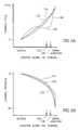
- FIGS. 2A, 2 B and 2 Cpresent experimental results of multiple programming and erase cycles, on log-linear charts.
- the gate voltage level for erasurewas increased, as necessary, and the cell ceased to function after 20,000 cycles.
- FIG. 2Agraphs the programming and erase threshold voltage levels for both bits.
- Curves 60 and 62illustrate the programming threshold voltage levels for the left and right bits, respectively, where the threshold voltage level for the right bit is measured in the forward (and not the reverse) direction.
- Curves 64 and 66illustrate the erase threshold voltage levels for the left and right bits, respectively. It is noted that all curves remain relatively constant until about 2000 cycles at which point the threshold voltage levels increase. It is also noted that the programming threshold voltage level for the left bit, read in the reverse direction, is significantly higher than that for the right bit. However, the erase threshold voltage levels of each bit are smaller than their programming threshold voltage levels.
- FIG. 2Billustrates the read current Ir after programming (curve 70 ) and after erasure (curve 72 ). The both currents decrease strongly after about 4000 cycles.
- FIG. 2Cillustrates the number of programming pulses (curve 74 ) and the gate voltage during erasure (curve 76 ).
- the number of programming pulsesdrops to one and the gate voltage drops from ⁇ 6V to ⁇ 9V after about 3000 cycles.
- An object of the present inventionis to provide an improved NROM cell which can endure an increased number of programming and erase cycles.
- an NROM cellhaving a double pocket implant self-aligned to at least one of its bit line junctions.
- the bit line junction(s)can have a thin area of effective programming and erasing located nearby.
- the channelcan have a threshold voltage level implant which has a low voltage level in a central area of the channel and which has a peak of high voltage level near at least one of the bit line junctions.
- the NROM cellincludes a channel, two diffusion areas on either side of the channel, each diffusion area having a junction with the channel, an oxide-nitride-oxide (ONO) layer over at least the channel, a polysilicon gate at least above the ONO layer and a pocket implant self-aligned to one or both of the junctions.
- ONOoxide-nitride-oxide
- the pocket implantcan be formed of one or two types of materials. If the latter is true, then the locations of maximum concentration of the two types of materials are separate from each other.
- the two types of materialsmight be Boron and Phosphorous wherein the Boron has a location of maximum concentration closer to the junction than the location of maximum concentration of the Phosphorous.
- a programmed bithas negative charge and an erased bit has positive charge stored in a portion of the ONO layer near the junction.
- the two oxide layers of the ONO layerare of 50-100 ⁇ and the nitride layer is 20-50 ⁇ .
- the Boron implantis 30-120 Kev up to a dose of 1-5 ⁇ 10 13 per cm 2 and the Phosphorous implant is 30-100 Kev up to a dose of 0.5-2.5 ⁇ 10 13 per cm 2 .
- the NROM cellcan include the channel, two diffusion areas on either side of the channel, an ONO layer, a polysilicon gate and a threshold voltage level implant which has a low voltage level in a central area of the channel and which has a peak of high voltage level near one or both of the junctions.
- a programmed bithas negative charge and an erased bit has positive charge stored in a portion of the ONO layer near the peak(s) of threshold voltage.
- a programmed bitraises the effective threshold voltage level in the area of the peak to a level above the high voltage level and an erased bit lowers the effective threshold voltage level in the area of the peak to the low voltage level.
- the NROM cellcan include the channel, two diffusion areas on either side of the channel, an ONO layer, a polysilicon gate and a thin area of effective programming and erasing located near one or both of the junctions.
- the NROM cellcan include the channel, two diffusion areas on either side of the channel, an ONO layer, a polysilicon gate and means for enabling generally full erasure of previously programmed charge.
- the NROM cellcan include the channel, two diffusion areas on either side of the channel, an ONO layer and a polysilicon gate.
- a programmed bithas negative charge and an erased bit has positive charge stored in portions of the ONO layer near one or both of the junctions.
- the amount of negative charge to be storedis less than twice a standard unit of negative charge.
- a programmed bithas a reduced electric field therein.
- FIGS. 1A, 1 B and 1 Care schematic illustrations of the operation of a prior art dual bit, nitride programmable read only memory (NROM) cell;
- FIGS. 2A, 2 B and 2 Care graphical illustrations of experimental results of multiple programming and erase cycles, on log-linear charts
- FIGS. 3A and 3Bare schematic illustrations of the state of the NROM cell of the prior art after the first cycle of programming and erasure, respectively;
- FIGS. 3C and 3Dare schematic illustrations of the state of the NROM cell of the prior art after the 20,000 th cycle of programming and erasure, respectively;
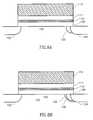
- FIGS. 4A and 4Bare schematic illustrations of two alternative embodiments of an NROM cell, constructed and operative in accordance with a preferred embodiment of the present invention, wherein the cell of FIG. 4A has single pocket implants and the cell of FIG. 4B has double pocket implants;
- FIGS. 5A and 5Bare graphical illustrations of the lateral channel field and the channel potential for the cells of FIGS. 4A and 4B;
- FIG. 6is a graphical illustration of the general shape of the threshold voltage level for the cells of FIGS. 4A and 4B;
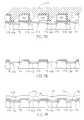
- FIGS. 7A, 7 B, 7 C, 7 D, 7 E and 7 Fare schematic illustrations of the manufacturing process for a row of NROM cells of the present invention.
- FIGS. 8A and 8Bare schematic illustrations of two single bit embodiments of an NROM cell, constructed and operative in accordance with a second preferred embodiment of the present invention, wherein the cell of FIG. 8A has a single pocket implant and the cell of FIG. 8B has a double pocket implant.
- FIGS. 3show the charge stored in right area 108 of the nitride layer as a function of distance along the channel for one cell.
- FIG. 3Ashows that, after the first cycle of programming, a significant amount of charge, labeled 80 , is stored close to the right bit line, which is the drain for programming and erasure. As one moves away from the drain, the amount of charge reduces, eventually to zero.
- FIG. 3Bshows the amount of charge, labeled 82 , left after the first erase cycle.
- the erase electric fieldis typically so effective that it removes extra electrons (more than were present in charge 80 ) such that section 82 is positive while section 80 is negative. Section 82 is thus, hatched, to indicate that it is positively charged.
- FIGS. 3C and 3Dparallel FIGS. 3A and 3B, respectively, but for after 20,000 cycles.
- FIGS. 3C and 3Dparallel FIGS. 3A and 3B, respectively, but for after 20,000 cycles.
- After programmingthere is a significant charge, labeled 84 , close to the drain, as in FIG. 3 A.
- FIG. 3 Athere is also another section of charge, labeled 86 , further from the drain, which diffused there over time and was not erased during from previous erase cycles. After the 20,000 th erase cycle, the extra section 86 still remains and is negatively charged, though the previously programmed section 84 has become positively charged section 88 .
- the diffused charge, in section 86is not erased during erasure operations and remains trapped there. Trapped charge 86 acts as partially programmed charge. It is due to trapped charge 86 that the fewer and fewer programming pulses are required to achieve the programmed threshold voltage level (since the bit is already, in effect, partially programmed) and that more and more erasure pulses are required to achieve the erase threshold voltage level (since trapped charge 86 is not removed).
- the trapped charge 86effects the reverse read (curves 60 and 64 of FIG. 2A) but not the forward read (curves 62 and 66 ), which is why the two sets of curves are so different.
- the negative charge far from the sourceaffects the reverse read since the forward read punches through the region under the trapped charge 86 .
- FIGS. 4A and 4Billustrate an NROM cell, constructed and operative in accordance with two preferred embodiments of the present invention.
- FIGS. 4A and 4Bare similar to FIG. 1 and thus, similar reference numerals refer to similar elements.
- FIGS. 5 A and 5 Bare graphs of the lateral channel field and the distribution of channel potential, respectively, for the NROM cells of FIGS. 4A and 4B and for a prior art NROM cell.
- the NROM cellcomprises the channel 100 between the bit lines 102 and 104 , the oxide-nitride-oxide sandwich of layers 109 , 110 , 111 , respectively, and the polysilicon gate 112 .
- a blanket threshold implantis present in the channel, though not shown specifically.
- the NROM cellcomprises either one or two extra implants self-aligned to each the junction of each bit line with the channel 100 .
- FIG. 4Ashows a Boron implant 120 and FIG. 4B shows Boron implant 120 with a Phosphorous implant 122 .
- the Boron implant 120is designed to have a maximum concentration near the bit line 102 or 104 while the Phosphorous implant 122 is designed to have a maximum concentration away from the bit line 102 or 104 .
- the single pocket implant of Boron 120in the embodiment of FIG. 4A, increases the threshold voltage level and, correspondingly, the lateral field, of the cell in the area near each bit line. Since Boron creates holes and Phosphorous creates free electrons, the combined profile, in the embodiment of FIG. 4B, is the difference of the two concentrations throughout the channel. Thus, the “double pocket” implant heightens the lateral field near the bit lines 102 and 104 but significantly reduces the lateral field in the rest of the channel 100 .
- the implantsare used to shape the lateral channel field so that it is high only close to the bit line junction and so that it drops significantly thereafter.
- FIGS. 5A and 5Bwhich graph of the channel field and potential, respectively, versus the location along the channel 100 for the right bit, for both embodiments and for the prior art.
- the left bit lineacts as the source and the right bit line acts as the drain.
- Position 130is the location of the maximum concentration of Boron and position 132 is the location of the maximum concentration of the Phosphorous implant, if present.
- curve 134indicates the lateral field with only a blanket threshold Vt implant
- curve 136indicates the lateral field with a single pocket implant
- curve 138indicates the lateral field with the double pocket implant.
- the lateral fieldhas a sharp dip 139 in the vicinity of the maximum concentration 132 of the Phosphorous implant and increases sharply toward the drain junction. It is noted that the lateral field is higher near the drain for the double implant than for either the single implant or no implant.
- Curve 140graphs the potential for an NROM cell without no implants
- curve 141graphs the potential of a cell with the single pocket implant
- curve 142graphs the potential of a cell with the double pocket implant.
- the channel potentialstarts at the 0V of the source and drops towards the negative Vd of the drain for all embodiments.
- the drain voltageis present only in the very close vicinity of the drain (curve 142 ).
- the drain voltageis spread over a slightly larger area near the drain while for the cell of no implants (curve 140 ), the drain voltage is spread over a significant area away from the drain.
- the single and double pocket implantsmaintain the effect of the drain voltage (high lateral field and strongly negative voltage level) in the vicinity of the drain.
- the double pocket implantthere is a sharp drop-off away from the drain.
- the generally thin area of effectforces the programmed charge to remain in a thin area of the nitride 110 (FIG. 4 ). This improves programming speed when programming ‘this’ bit. Furthermore, since the programmed charge is maintained in an area near the drain, the erase voltage generally removes all of the charge for this bit. The thin area of effect also ensures effective punchthrough when reading the ‘other’ bit.
- the threshold voltage levelis low (labeled 150 ) throughout most of the channel with peaks 152 near the bit line junctions 102 and 104 .
- the height and width of the peaks 152is a function of the number of implants (one or two) and the locations of maximum concentration of the implant or implants.
- the general threshold voltage level 150is at a low level, of about 1V, while the peaks 152 reach a much higher level, such as about 2V.
- the threshold voltage level of the cellstarts higher than the standard 1.5V. Furthermore, once a bit has been programmed, for example, with a single unit ⁇ Q of charge, the threshold voltage level in the area of interest rises to a programmed level 154 , such as of 3V.
- the programmed threshold voltage levelis indicated with dashed lines.
- the threshold voltage level of the celldrops to the general level 150 of the center of the cell. As this is below the original threshold voltage level 152 in the drain area, the cell is now erased to a positive charge level, for example of +Q, at least in the area near the bit line junction.
- a positive charge levelfor example of +Q
- To reprogram the cellone must provide enough negative charge to counter the positive erase state and to bring the cell to the negative level of being programmed. This is opposed to the prior art which programs to the negative level of being programmed (e.g. ⁇ 2Q) and erases to the initial, non-charged state (e.g. 0).
- the low amounts of chargereduce the size of the field caused by the presence of charge within the nitride layer. This reduced field helps retain the charge within its desired location.
- the general level 150 of the center of the cellcan be set to any desired low level.
- FIGS. 7A, 7 B, 7 C, 7 D, 7 E and 7 Fillustrate an exemplary method of producing the cell of the present invention.
- the oxide, nitride and oxide layers 160 , 162 and 164are grown on top of a substrate 166 , to form the basis of the ONO structure.
- Typical thicknesses of layers 160 , 162 and 164are 50-100 ⁇ , 20-50 ⁇ , 50-100 ⁇ , respectively.
- a p-well or blanket threshold implant, of 5-10 3 per cm 3can be provided to the substrate 166 prior to growing the ONO layers.
- a bit line mask 168is laid down next.
- the maskis formed of columns laid over the locations of the future channels.
- the bit linesare to be implanted between the columns 168 and are thus, self-aligned to the future channels.
- the bit line maskcan be formed of a hardened photoresist or of a thick oxide.
- the bit line mask 168is a layer of photoresist hardened with ultraviolet (UV) after being laid down. This makes a hard mask which is not removable using the standard photoresist removal solvents.
- UVultraviolet
- An alternative bit line mask 168can be formed of a thick oxide layer, of a minimal thickness of 1000 ⁇ .
- Such a maskis formed by first depositing a thick oxide layer, typically utilizing the low pressure, chemical vapor deposit (LPCVD) process. A layer of photoresist is then deposited in the desired column pattern after which the oxide found between the photoresist columns is etched away, typically using a dry etch process. The photoresist layer is removed and the thick oxide, bit line mask 168 remains. The thick oxide mask cannot be removed during standard, solvent, photoresist removal techniques.
- LPCVDlow pressure, chemical vapor deposit
- the ONO layersare etched, using a dry etch or wet/dry combination, to remove the oxide and nitride layers between the columns of the bit line mask 168 .
- the lower oxide layer 160remains between the columns of the bit line mask 168 to implant through the oxide. This is commonly performed in the art to reduce channeling.
- bit lines 104are then implanted between the columns of the bit line mask 168 .
- the implant operationis 45 Kev of Arsenic, up to a dose of 2-6 ⁇ 10 15 per cm 2 .
- Other implants and dosage levelsare also contemplated and are within the scope of the present invention.
- bit line junctions of each cellare separately implanted.
- a threshold pocket implantof one or two implant materials, is provided at an angle to the vertical, thereby implanting, in a self-aligned manner, into the bit line junctions as well as into part of the open bit lines near the bit line junctions. The process is then repeated for the other side.
- FIG. 7Cshows the operation for left bit line junctions 170 of one row of cells and indicates the threshold implant with arrows 172 .
- the implantcan be any suitable threshold pocket implant. For a single implant, it can be Boron at 30-120 Kev up to a dose of 1-5 ⁇ 10 13 per cm 2 .
- the second implantif there is one, can be Phosphorous at 30-100 Kev up to a dose of 0.5-2.5 ⁇ 10 13 per cm 2 .
- the remaining discussion of the manufacturing processwill use the term “implant” to refer to either a single implant or a double implant unless otherwise stated.
- the implantis at an angle of 15-45° to the right of vertical. Since the bit line mask 168 covers the channels of all cells, the implant has access only to the left bit line junctions. The implant is to the right of the vertical since the left bit line junctions are on the right of the open bit lines (which is to the left of the neighboring channel). As indicated by the arrows 172 , the angled implant accesses the left bit line junction and a portion of the open bit lines to the left of the junction. The implant is, thus, self-aligned to the left bit line junctions 170 of the channels.
- the choice of angleis typically based on the desired location of maximum concentration for each implant material and is typically 15-45°.
- the thickness of the bit line mask 168affects the amount of shadowing and is a function of the angle of the implant, as follows:
- the thickness h 1is 2197 ⁇ .
- FIG. 7Dillustrates the threshold implant operation for the right bit line junctions 176 .
- the implantlabeled by arrows 174 , is at the same angle as before; however, for the right bit line junctions 176 , the implant angle is to the left of vertical.
- bit line mask 168is both a bit line mask and a threshold pocket implant mask.
- bit line implantcan occur before the pocket implants, as shown, or afterwards. It will further be appreciated that the order for implanting the pocket implant into the right and left bit line junctions is not significant nor does it affect the self-alignment of the implants to the bit line junctions.
- bit line mask 168is removed.
- this processinvolves a plasma removal process of the top photoresist layer followed by standard solvent photoresist removal techniques. If the bit line mask 168 is formed of a thick oxide layer, it is removed with a standard wet etch.
- the sacrificial oxide layer 160is removed using a wet etch. The result is shown in FIG. 7 E. Within substrate 166 are the bit lines 104 and the implanted bit line junctions 170 and 176 . If the bit line mask 168 is formed of a thick oxide layer, the sacrificial oxide layer 160 is removed together with the bit line mask.
- CMOScomplementary, metal-oxide semiconductor
- the gate oxide layer 20is 2-3 times thicker over the bit lines 104 due to the presence therein of the bit line implant material. If the gate oxide is deposited, this is not true.
- the final stepis the deposition of the polysilicon gates and word lines, in accordance with standard deposition techniques.
- the resultis the row shown in FIG. 7 E.
- FIGS. 8A and 8Bshow alternative embodiments of the present invention for single bit NROM cells.
- FIG. 8Ashows an NROM cell having a single pocket implant 120 on the right side of the cell while
- FIG. 8Bshows an NROM cell having two pocket implants 120 and 122 on the right side of the cell.
- FIGS. 8A and 8Bhave the same properties as the double bit cells of FIGS. 4A and 4B.
- the improved qualities of the lateral field and channel potential of FIGS. 5A and 5B, respectively,are applicable to the cells of FIGS. 8A and 8B during programming, when the right bit line 104 is the drain.
Landscapes
- Engineering & Computer Science (AREA)
- Microelectronics & Electronic Packaging (AREA)
- Computer Hardware Design (AREA)
- Non-Volatile Memory (AREA)
- Semiconductor Memories (AREA)
Abstract
Description
Claims (4)
Priority Applications (1)
| Application Number | Priority Date | Filing Date | Title |
|---|---|---|---|
| US09/778,502US6477084B2 (en) | 1998-05-20 | 2001-02-07 | NROM cell with improved programming, erasing and cycling |
Applications Claiming Priority (2)
| Application Number | Priority Date | Filing Date | Title |
|---|---|---|---|
| US09/082,280US6215148B1 (en) | 1998-05-20 | 1998-05-20 | NROM cell with improved programming, erasing and cycling |
| US09/778,502US6477084B2 (en) | 1998-05-20 | 2001-02-07 | NROM cell with improved programming, erasing and cycling |
Related Parent Applications (1)
| Application Number | Title | Priority Date | Filing Date |
|---|---|---|---|
| US09/082,280DivisionUS6215148B1 (en) | 1998-05-20 | 1998-05-20 | NROM cell with improved programming, erasing and cycling |
Publications (2)
| Publication Number | Publication Date |
|---|---|
| US20010004332A1 US20010004332A1 (en) | 2001-06-21 |
| US6477084B2true US6477084B2 (en) | 2002-11-05 |
Family
ID=22170207
Family Applications (2)
| Application Number | Title | Priority Date | Filing Date |
|---|---|---|---|
| US09/082,280Expired - LifetimeUS6215148B1 (en) | 1998-05-20 | 1998-05-20 | NROM cell with improved programming, erasing and cycling |
| US09/778,502Expired - LifetimeUS6477084B2 (en) | 1998-05-20 | 2001-02-07 | NROM cell with improved programming, erasing and cycling |
Family Applications Before (1)
| Application Number | Title | Priority Date | Filing Date |
|---|---|---|---|
| US09/082,280Expired - LifetimeUS6215148B1 (en) | 1998-05-20 | 1998-05-20 | NROM cell with improved programming, erasing and cycling |
Country Status (5)
| Country | Link |
|---|---|
| US (2) | US6215148B1 (en) |
| EP (1) | EP1082763A4 (en) |
| JP (1) | JP2002516491A (en) |
| AU (1) | AU3845399A (en) |
| WO (1) | WO1999060631A1 (en) |
Cited By (73)
| Publication number | Priority date | Publication date | Assignee | Title |
|---|---|---|---|---|
| US20030119213A1 (en)* | 2001-12-20 | 2003-06-26 | Ming-Hung Chou | Pre-erase manufacturing method |
| US20030234421A1 (en)* | 2002-06-21 | 2003-12-25 | Chang Kent Kuohua | Structure of discrete nrom cell |
| US20030235075A1 (en)* | 2002-06-21 | 2003-12-25 | Micron Technology, Inc. | Vertical NROM having a storage density of 1bit per 1F2 |
| US6830963B1 (en) | 2003-10-09 | 2004-12-14 | Micron Technology, Inc. | Fully depleted silicon-on-insulator CMOS logic |
| US20050030794A1 (en)* | 2003-08-07 | 2005-02-10 | Micron Technology, Inc. | Method for erasing an NROM cell |
| US20050030792A1 (en)* | 2003-08-07 | 2005-02-10 | Micron Technology, Inc. | Method for programming and erasing an nrom cell |
| US6872609B1 (en) | 2004-01-12 | 2005-03-29 | Advanced Micro Devices, Inc. | Narrow bitline using Safier for mirrorbit |
| US6878991B1 (en) | 2004-01-30 | 2005-04-12 | Micron Technology, Inc. | Vertical device 4F2 EEPROM memory |
| US20050101065A1 (en)* | 2003-10-01 | 2005-05-12 | Susumu Inoue | Method of manufacturing a semiconductor device |
| US20050106811A1 (en)* | 2003-11-17 | 2005-05-19 | Micron Technology, Inc. | NROM flash memory devices on ultrathin silicon |
| US20050138262A1 (en)* | 2003-12-18 | 2005-06-23 | Micron Technology, Inc. | Flash memory having a high-permittivity tunnel dielectric |
| US20050153508A1 (en)* | 2004-01-12 | 2005-07-14 | Lingunis Emmanuil H. | Pocket implant for complementary bit disturb improvement and charging improvement of SONOS memory cell |
| US20050164456A1 (en)* | 2002-06-28 | 2005-07-28 | Joachim Deppe | Method for fabricating an NROM memory cell array |
| US20050174847A1 (en)* | 2004-02-10 | 2005-08-11 | Micron Technology, Inc. | Nrom flash memory cell with integrated dram |
| US20050173755A1 (en)* | 2004-02-10 | 2005-08-11 | Micron Technology, Inc. | NROM flash memory with a high-permittivity gate dielectric |
| US20050185466A1 (en)* | 2004-02-24 | 2005-08-25 | Micron Technology, Inc. | Multi-state memory cell with asymmetric charge trapping |
| US20050189582A1 (en)* | 2004-02-10 | 2005-09-01 | Thomas Mikolajick | Charge trapping memory cell and fabrication method |
| US20050195650A1 (en)* | 2004-03-05 | 2005-09-08 | Joachim Deppe | Method for operating an electrical writable and erasable memory cell and a memory device for electrical memories |
| US20050196923A1 (en)* | 2002-09-04 | 2005-09-08 | Joachim Deppe | SONOS memory cells and arrays and method of forming the same |
| US20050212033A1 (en)* | 2004-03-24 | 2005-09-29 | Micron Technology, Inc. | Memory device with high dielectric constant gate dielectrics and metal floating gates |
| US6962849B1 (en) | 2003-12-05 | 2005-11-08 | Advanced Micro Devices, Inc. | Hard mask spacer for sublithographic bitline |
| US20050247972A1 (en)* | 2004-05-06 | 2005-11-10 | Micron Technology, Inc. | Ballistic direct injection NROM cell on strained silicon structures |
| US20050255638A1 (en)* | 2003-09-05 | 2005-11-17 | Micron Technology, Inc. | Trench corner effect bidirectional flash memory cell |
| US20050255651A1 (en)* | 2004-05-11 | 2005-11-17 | Weidong Qian | Bitline implant utilizing dual poly |
| US20050265080A1 (en)* | 2004-05-27 | 2005-12-01 | Renesas Technology Corp. | Semiconductor nonvolatile memory device |
| US6979857B2 (en) | 2003-07-01 | 2005-12-27 | Micron Technology, Inc. | Apparatus and method for split gate NROM memory |
| US20050286296A1 (en)* | 2002-12-12 | 2005-12-29 | Michael Bollu | Semiconductor memory having charge trapping memory cells and fabrication method |
| US7050330B2 (en) | 2003-12-16 | 2006-05-23 | Micron Technology, Inc. | Multi-state NROM device |
| US7075146B2 (en) | 2004-02-24 | 2006-07-11 | Micron Technology, Inc. | 4F2 EEPROM NROM memory arrays with vertical devices |
| US7095075B2 (en) | 2003-07-01 | 2006-08-22 | Micron Technology, Inc. | Apparatus and method for split transistor memory having improved endurance |
| US7125763B1 (en)* | 2000-09-29 | 2006-10-24 | Spansion Llc | Silicided buried bitline process for a non-volatile memory cell |
| US20060281262A1 (en)* | 2005-05-23 | 2006-12-14 | Digh Hisamoto | Integrated semiconductor nonvolatile storage device |
| US20070031999A1 (en)* | 2005-08-04 | 2007-02-08 | Macronix International Co. Ltd. | Non-volatile memory cells and methods of manufacturing the same |
| US7176113B1 (en) | 2004-06-07 | 2007-02-13 | Spansion Llc | LDC implant for mirrorbit to improve Vt roll-off and form sharper junction |
| US20070040211A1 (en)* | 2005-08-22 | 2007-02-22 | Macronix International Co., Ltd. | Nonvolatile memory device and method of forming the same |
| US7184315B2 (en) | 2003-11-04 | 2007-02-27 | Micron Technology, Inc. | NROM flash memory with self-aligned structural charge separation |
| US7220634B2 (en) | 2002-06-21 | 2007-05-22 | Micron Technology, Inc. | NROM memory cell, memory array, related devices and methods |
| US7241654B2 (en) | 2003-12-17 | 2007-07-10 | Micron Technology, Inc. | Vertical NROM NAND flash memory array |
| US7259422B1 (en) | 2006-03-13 | 2007-08-21 | Renesas Technology Corp. | Nonvolatile semiconductor memory device and its fabrication method |
| US7269072B2 (en) | 2003-12-16 | 2007-09-11 | Micron Technology, Inc. | NROM memory cell, memory array, related devices and methods |
| US20080073705A1 (en)* | 2006-09-21 | 2008-03-27 | Digh Hisamoto | Semiconductor device |
| US7369440B2 (en) | 2005-01-19 | 2008-05-06 | Saifun Semiconductors Ltd. | Method, circuit and systems for erasing one or more non-volatile memory cells |
| US20080108197A1 (en)* | 2004-06-17 | 2008-05-08 | Samsung Electronics Co., Ltd. | Method of fabricating non-volatile flash memory device having at least two different channel concentrations |
| US20080111182A1 (en)* | 2006-11-02 | 2008-05-15 | Rustom Irani | Forming buried contact etch stop layer (CESL) in semiconductor devices self-aligned to diffusion |
| US20080128774A1 (en)* | 2006-11-02 | 2008-06-05 | Rustom Irani | Forming silicon trench isolation (STI) in semiconductor devices self-aligned to diffusion |
| US7405969B2 (en) | 1997-08-01 | 2008-07-29 | Saifun Semiconductors Ltd. | Non-volatile memory cell and non-volatile memory devices |
| US20080185635A1 (en)* | 2007-02-01 | 2008-08-07 | Renesas Technology Corp. | Semiconductor storage device and manufacturing method thereof |
| US20080192544A1 (en)* | 2007-02-13 | 2008-08-14 | Amit Berman | Error correction coding techniques for non-volatile memory |
| US7457183B2 (en) | 2003-09-16 | 2008-11-25 | Saifun Semiconductors Ltd. | Operating array cells with matched reference cells |
| US7466594B2 (en) | 2004-08-12 | 2008-12-16 | Saifun Semiconductors Ltd. | Dynamic matching of signal path and reference path for sensing |
| US20090003073A1 (en)* | 2006-01-10 | 2009-01-01 | Arik Rizel | Rd Algorithm Improvement for Nrom Technology |
| US20090065841A1 (en)* | 2007-09-06 | 2009-03-12 | Assaf Shappir | SILICON OXY-NITRIDE (SiON) LINER, SUCH AS OPTIONALLY FOR NON-VOLATILE MEMORY CELLS |
| US20090073760A1 (en)* | 2007-09-17 | 2009-03-19 | Yoram Betser | Minimizing read disturb in an array flash cell |
| US20090073774A1 (en)* | 2007-09-17 | 2009-03-19 | Yaal Horesh | Pre-charge sensing scheme for non-volatile memory (NVM) |
| US20090109755A1 (en)* | 2007-10-24 | 2009-04-30 | Mori Edan | Neighbor block refresh for non-volatile memory |
| US20090122610A1 (en)* | 2007-11-14 | 2009-05-14 | Kobi Danon | Operation of a non-volatile memory array |
| US7535765B2 (en) | 2004-12-09 | 2009-05-19 | Saifun Semiconductors Ltd. | Non-volatile memory device and method for reading cells |
| US20090175089A1 (en)* | 2008-01-08 | 2009-07-09 | Boaz Eitan | Retention in NVM with top or bottom injection |
| US20090204747A1 (en)* | 2007-11-01 | 2009-08-13 | Avi Lavan | Non binary flash array architecture and method of operation |
| US20090228739A1 (en)* | 2007-11-25 | 2009-09-10 | Itzic Cohen | Recovery while programming non-volatile memory (nvm) |
| US7605579B2 (en) | 2006-09-18 | 2009-10-20 | Saifun Semiconductors Ltd. | Measuring and controlling current consumption and output current of charge pumps |
| US20090309153A1 (en)* | 2008-06-13 | 2009-12-17 | Renesas Technology Corp. | Method of manufacturing semiconductor device and semiconductor device |
| US7638835B2 (en) | 2006-02-28 | 2009-12-29 | Saifun Semiconductors Ltd. | Double density NROM with nitride strips (DDNS) |
| US20090323423A1 (en)* | 2006-09-12 | 2009-12-31 | Ilan Bloom | Methods, circuits and systems for reading non-volatile memory cells |
| US7675782B2 (en) | 2002-10-29 | 2010-03-09 | Saifun Semiconductors Ltd. | Method, system and circuit for programming a non-volatile memory array |
| US7692961B2 (en) | 2006-02-21 | 2010-04-06 | Saifun Semiconductors Ltd. | Method, circuit and device for disturb-control of programming nonvolatile memory cells by hot-hole injection (HHI) and by channel hot-electron (CHE) injection |
| US7701779B2 (en) | 2006-04-27 | 2010-04-20 | Sajfun Semiconductors Ltd. | Method for programming a reference cell |
| US7743230B2 (en) | 2003-01-31 | 2010-06-22 | Saifun Semiconductors Ltd. | Memory array programming circuit and a method for using the circuit |
| US7808818B2 (en) | 2006-01-12 | 2010-10-05 | Saifun Semiconductors Ltd. | Secondary injection for NROM |
| US20110001179A1 (en)* | 2009-07-03 | 2011-01-06 | Renesas Electronics Corporation | Semiconductor device and manufacturing method of the same |
| US7964459B2 (en) | 2004-10-14 | 2011-06-21 | Spansion Israel Ltd. | Non-volatile memory structure and method of fabrication |
| US8471328B2 (en) | 2010-07-26 | 2013-06-25 | United Microelectronics Corp. | Non-volatile memory and manufacturing method thereof |
| US20130194866A1 (en)* | 2009-07-10 | 2013-08-01 | Macronix International Co., Ltd. | Accessing method and a memory using thereof |
Families Citing this family (129)
| Publication number | Priority date | Publication date | Assignee | Title |
|---|---|---|---|---|
| IL125604A (en) | 1997-07-30 | 2004-03-28 | Saifun Semiconductors Ltd | Non-volatile electrically erasable and programmble semiconductor memory cell utilizing asymmetrical charge |
| US6348711B1 (en)* | 1998-05-20 | 2002-02-19 | Saifun Semiconductors Ltd. | NROM cell with self-aligned programming and erasure areas |
| WO2000070675A1 (en)* | 1999-05-14 | 2000-11-23 | Hitachi, Ltd. | Semiconductor memory device |
| JP2001148434A (en)* | 1999-10-12 | 2001-05-29 | New Heiro:Kk | Nonvolatile memory cell, method of using the same, manufacturing method, and nonvolatile memory array |
| JP3829161B2 (en)* | 1999-10-14 | 2006-10-04 | スパンション インク | Nonvolatile memory circuit for recording multi-bit information |
| US6429063B1 (en) | 1999-10-26 | 2002-08-06 | Saifun Semiconductors Ltd. | NROM cell with generally decoupled primary and secondary injection |
| JP4899241B2 (en)* | 1999-12-06 | 2012-03-21 | ソニー株式会社 | Nonvolatile semiconductor memory device and operation method thereof |
| US6532556B1 (en) | 2000-01-27 | 2003-03-11 | Multi Level Memory Technology | Data management for multi-bit-per-cell memories |
| US6438031B1 (en)* | 2000-02-16 | 2002-08-20 | Advanced Micro Devices, Inc. | Method of programming a non-volatile memory cell using a substrate bias |
| US6396741B1 (en)* | 2000-05-04 | 2002-05-28 | Saifun Semiconductors Ltd. | Programming of nonvolatile memory cells |
| US6928001B2 (en)* | 2000-12-07 | 2005-08-09 | Saifun Semiconductors Ltd. | Programming and erasing methods for a non-volatile memory cell |
| JP4002712B2 (en)* | 2000-05-15 | 2007-11-07 | スパンション エルエルシー | Nonvolatile semiconductor memory device and data holding method of nonvolatile semiconductor memory device |
| US6275414B1 (en)* | 2000-05-16 | 2001-08-14 | Advanced Micro Devices, Inc. | Uniform bitline strapping of a non-volatile memory cell |
| US6593606B1 (en) | 2000-05-16 | 2003-07-15 | Advanced Micro Devices, Inc. | Staggered bitline strapping of a non-volatile memory cell |
| US6538270B1 (en) | 2000-05-16 | 2003-03-25 | Advanced Micro Devices, Inc. | Staggered bitline strapping of a non-volatile memory cell |
| US6618290B1 (en)* | 2000-06-23 | 2003-09-09 | Advanced Micro Devices, Inc. | Method of programming a non-volatile memory cell using a baking process |
| JP4837230B2 (en)* | 2000-07-17 | 2011-12-14 | スパンション エルエルシー | Semiconductor non-volatile memory device and manufacturing method thereof |
| US6750157B1 (en) | 2000-10-12 | 2004-06-15 | Advanced Micro Devices, Inc. | Nonvolatile memory cell with a nitridated oxide layer |
| US6468865B1 (en) | 2000-11-28 | 2002-10-22 | Advanced Micro Devices, Inc. | Method of simultaneous formation of bitline isolation and periphery oxide |
| US6465306B1 (en) | 2000-11-28 | 2002-10-15 | Advanced Micro Devices, Inc. | Simultaneous formation of charge storage and bitline to wordline isolation |
| US6614692B2 (en)* | 2001-01-18 | 2003-09-02 | Saifun Semiconductors Ltd. | EEPROM array and method for operation thereof |
| JP2002231918A (en)* | 2001-02-06 | 2002-08-16 | Olympus Optical Co Ltd | Solid-state imaging device and manufacturing method thereof |
| US6456533B1 (en) | 2001-02-28 | 2002-09-24 | Advanced Micro Devices, Inc. | Higher program VT and faster programming rates based on improved erase methods |
| ATE458249T1 (en)* | 2001-03-15 | 2010-03-15 | Halo Inc | DOUBLE BIT MONOS MEMORY CELL USE FOR WIDE PROGRAM BANDWIDTH |
| JP2002279787A (en)* | 2001-03-16 | 2002-09-27 | Hitachi Ltd | Nonvolatile semiconductor memory device |
| JP4696383B2 (en)* | 2001-03-28 | 2011-06-08 | ソニー株式会社 | Method for manufacturing nonvolatile semiconductor memory device |
| US6584017B2 (en)* | 2001-04-05 | 2003-06-24 | Saifun Semiconductors Ltd. | Method for programming a reference cell |
| US6493266B1 (en)* | 2001-04-09 | 2002-12-10 | Advanced Micro Devices, Inc. | Soft program and soft program verify of the core cells in flash memory array |
| DE10129958B4 (en) | 2001-06-21 | 2006-07-13 | Infineon Technologies Ag | Memory cell arrangement and manufacturing method |
| US6436768B1 (en) | 2001-06-27 | 2002-08-20 | Advanced Micro Devices, Inc. | Source drain implant during ONO formation for improved isolation of SONOS devices |
| US6903977B2 (en)* | 2001-09-25 | 2005-06-07 | Sony Corporation | Nonvolatile semiconductor memory device and method of producing the same |
| US6630384B1 (en) | 2001-10-05 | 2003-10-07 | Advanced Micro Devices, Inc. | Method of fabricating double densed core gates in sonos flash memory |
| CN1324691C (en)* | 2001-10-22 | 2007-07-04 | 旺宏电子股份有限公司 | Erasing method of P-type channel silicon nitride read-only memory |
| US6791396B2 (en)* | 2001-10-24 | 2004-09-14 | Saifun Semiconductors Ltd. | Stack element circuit |
| US6643181B2 (en) | 2001-10-24 | 2003-11-04 | Saifun Semiconductors Ltd. | Method for erasing a memory cell |
| US6925007B2 (en)* | 2001-10-31 | 2005-08-02 | Sandisk Corporation | Multi-state non-volatile integrated circuit memory systems that employ dielectric storage elements |
| US6897522B2 (en) | 2001-10-31 | 2005-05-24 | Sandisk Corporation | Multi-state non-volatile integrated circuit memory systems that employ dielectric storage elements |
| CN100438037C (en)* | 2001-11-07 | 2008-11-26 | 旺宏电子股份有限公司 | Multi-level NROM memory cell and operation method thereof |
| DE10201304A1 (en)* | 2002-01-15 | 2003-07-31 | Infineon Technologies Ag | Non-volatile semiconductor memory cell and associated manufacturing process |
| US6975536B2 (en)* | 2002-01-31 | 2005-12-13 | Saifun Semiconductors Ltd. | Mass storage array and methods for operation thereof |
| US7190620B2 (en)* | 2002-01-31 | 2007-03-13 | Saifun Semiconductors Ltd. | Method for operating a memory device |
| US6700818B2 (en)* | 2002-01-31 | 2004-03-02 | Saifun Semiconductors Ltd. | Method for operating a memory device |
| DE60212938D1 (en)* | 2002-04-30 | 2006-08-17 | St Microelectronics Srl | Method for reducing unwanted deletion when programming a nonvolatile NROM |
| US6747896B2 (en) | 2002-05-06 | 2004-06-08 | Multi Level Memory Technology | Bi-directional floating gate nonvolatile memory |
| US6914820B1 (en) | 2002-05-06 | 2005-07-05 | Multi Level Memory Technology | Erasing storage nodes in a bi-directional nonvolatile memory cell |
| US7221591B1 (en)* | 2002-05-06 | 2007-05-22 | Samsung Electronics Co., Ltd. | Fabricating bi-directional nonvolatile memory cells |
| US6816412B2 (en)* | 2002-05-21 | 2004-11-09 | Broadcom Corporation | Non-volatile memory cell techniques |
| JP3637332B2 (en)* | 2002-05-29 | 2005-04-13 | 株式会社東芝 | Semiconductor device and manufacturing method thereof |
| DE10226964A1 (en) | 2002-06-17 | 2004-01-08 | Infineon Technologies Ag | Method for manufacturing an NROM memory cell arrangement |
| US6804136B2 (en)* | 2002-06-21 | 2004-10-12 | Micron Technology, Inc. | Write once read only memory employing charge trapping in insulators |
| US7221586B2 (en) | 2002-07-08 | 2007-05-22 | Micron Technology, Inc. | Memory utilizing oxide nanolaminates |
| US6917544B2 (en) | 2002-07-10 | 2005-07-12 | Saifun Semiconductors Ltd. | Multiple use memory chip |
| DE10232938B4 (en)* | 2002-07-19 | 2005-05-04 | Infineon Technologies Ag | Method for producing a buried bit line for a semiconductor memory |
| US6826107B2 (en)* | 2002-08-01 | 2004-11-30 | Saifun Semiconductors Ltd. | High voltage insertion in flash memory cards |
| DE10239491A1 (en)* | 2002-08-28 | 2004-03-18 | Infineon Technologies Ag | Production of trenched bit lines in a semiconductor memory comprises using a mask which is produced whilst an auxiliary layer is applied on the whole surface and structured using a lacquer mask |
| US6707078B1 (en) | 2002-08-29 | 2004-03-16 | Fasl, Llc | Dummy wordline for erase and bitline leakage |
| JP2004095889A (en) | 2002-08-30 | 2004-03-25 | Fasl Japan Ltd | Semiconductor storage device and method of manufacturing the same |
| DE10240916A1 (en)* | 2002-09-04 | 2004-03-25 | Infineon Technologies Ag | Production of a memory cell field used in charge trapping memory cells, e.g. NROM memory cells comprises forming insulating trenches between trenches whilst a hard mask is applied on or above the upper side of the semiconductor body |
| DE10241990B4 (en)* | 2002-09-11 | 2006-11-09 | Infineon Technologies Ag | Method for structuring layers on semiconductor devices |
| JP4572500B2 (en)* | 2002-12-27 | 2010-11-04 | ソニー株式会社 | Nonvolatile semiconductor memory device and operation method thereof |
| US7151292B1 (en)* | 2003-01-15 | 2006-12-19 | Spansion Llc | Dielectric memory cell structure with counter doped channel region |
| US6967896B2 (en)* | 2003-01-30 | 2005-11-22 | Saifun Semiconductors Ltd | Address scramble |
| JP4256198B2 (en)* | 2003-04-22 | 2009-04-22 | 株式会社東芝 | Data storage system |
| US7142464B2 (en)* | 2003-04-29 | 2006-11-28 | Saifun Semiconductors Ltd. | Apparatus and methods for multi-level sensing in a memory array |
| DE10324052B4 (en)* | 2003-05-27 | 2007-06-28 | Infineon Technologies Ag | Method for producing a semiconductor memory with charge trapping memory cells |
| JP2005024665A (en)* | 2003-06-30 | 2005-01-27 | Ricoh Co Ltd | Powder conveying apparatus, image forming apparatus, toner container, and process cartridge |
| US20050251617A1 (en)* | 2004-05-07 | 2005-11-10 | Sinclair Alan W | Hybrid non-volatile memory system |
| US7151692B2 (en) | 2004-01-27 | 2006-12-19 | Macronix International Co., Ltd. | Operation scheme for programming charge trapping non-volatile memory |
| US7018868B1 (en) | 2004-02-02 | 2006-03-28 | Advanced Micro Devices, Inc. | Disposable hard mask for memory bitline scaling |
| US6927145B1 (en) | 2004-02-02 | 2005-08-09 | Advanced Micro Devices, Inc. | Bitline hard mask spacer flow for memory cell scaling |
| US7209389B2 (en)* | 2004-02-03 | 2007-04-24 | Macronix International Co., Ltd. | Trap read only non-volatile memory (TROM) |
| US20050205969A1 (en)* | 2004-03-19 | 2005-09-22 | Sharp Laboratories Of America, Inc. | Charge trap non-volatile memory structure for 2 bits per transistor |
| WO2005094178A2 (en)* | 2004-04-01 | 2005-10-13 | Saifun Semiconductors Ltd. | Method, circuit and systems for erasing one or more non-volatile memory cells |
| US7158411B2 (en)* | 2004-04-01 | 2007-01-02 | Macronix International Co., Ltd. | Integrated code and data flash memory |
| US7187590B2 (en)* | 2004-04-26 | 2007-03-06 | Macronix International Co., Ltd. | Method and system for self-convergent erase in charge trapping memory cells |
| US7209390B2 (en)* | 2004-04-26 | 2007-04-24 | Macronix International Co., Ltd. | Operation scheme for spectrum shift in charge trapping non-volatile memory |
| US7075828B2 (en)* | 2004-04-26 | 2006-07-11 | Macronix International Co., Intl. | Operation scheme with charge balancing erase for charge trapping non-volatile memory |
| US7164603B2 (en)* | 2004-04-26 | 2007-01-16 | Yen-Hao Shih | Operation scheme with high work function gate and charge balancing for charge trapping non-volatile memory |
| US7133313B2 (en)* | 2004-04-26 | 2006-11-07 | Macronix International Co., Ltd. | Operation scheme with charge balancing for charge trapping non-volatile memory |
| US7366025B2 (en)* | 2004-06-10 | 2008-04-29 | Saifun Semiconductors Ltd. | Reduced power programming of non-volatile cells |
| US7190614B2 (en)* | 2004-06-17 | 2007-03-13 | Macronix International Co., Ltd. | Operation scheme for programming charge trapping non-volatile memory |
| US7106625B2 (en)* | 2004-07-06 | 2006-09-12 | Macronix International Co, Td | Charge trapping non-volatile memory with two trapping locations per gate, and method for operating same |
| US20060007732A1 (en)* | 2004-07-06 | 2006-01-12 | Macronix International Co., Ltd. | Charge trapping non-volatile memory and method for operating same |
| US7317633B2 (en) | 2004-07-06 | 2008-01-08 | Saifun Semiconductors Ltd | Protection of NROM devices from charge damage |
| US6903410B1 (en)* | 2004-08-02 | 2005-06-07 | Macronix International Co., Ltd | Electrically erasable programmable read only memory cell and programming method thereof |
| JP2006120719A (en)* | 2004-10-19 | 2006-05-11 | Fujitsu Ltd | Nonvolatile semiconductor memory device and manufacturing method thereof |
| US7133317B2 (en)* | 2004-11-19 | 2006-11-07 | Macronix International Co., Ltd. | Method and apparatus for programming nonvolatile memory |
| US20060113586A1 (en)* | 2004-11-29 | 2006-06-01 | Macronix International Co., Ltd. | Charge trapping dielectric structure for non-volatile memory |
| CN100386883C (en)* | 2004-12-15 | 2008-05-07 | 旺宏电子股份有限公司 | Nonvolatile memory cell, operating method thereof and nonvolatile memory |
| US8482052B2 (en) | 2005-01-03 | 2013-07-09 | Macronix International Co., Ltd. | Silicon on insulator and thin film transistor bandgap engineered split gate memory |
| US7315474B2 (en) | 2005-01-03 | 2008-01-01 | Macronix International Co., Ltd | Non-volatile memory cells, memory arrays including the same and methods of operating cells and arrays |
| US7473589B2 (en)* | 2005-12-09 | 2009-01-06 | Macronix International Co., Ltd. | Stacked thin film transistor, non-volatile memory devices and methods for fabricating the same |
| US8053812B2 (en) | 2005-03-17 | 2011-11-08 | Spansion Israel Ltd | Contact in planar NROM technology |
| US7158420B2 (en)* | 2005-04-29 | 2007-01-02 | Macronix International Co., Ltd. | Inversion bit line, charge trapping non-volatile memory and method of operating same |
| US7301219B2 (en)* | 2005-06-06 | 2007-11-27 | Macronix International Co., Ltd. | Electrically erasable programmable read only memory (EEPROM) cell and method for making the same |
| US8400841B2 (en)* | 2005-06-15 | 2013-03-19 | Spansion Israel Ltd. | Device to program adjacent storage cells of different NROM cells |
| US7184313B2 (en)* | 2005-06-17 | 2007-02-27 | Saifun Semiconductors Ltd. | Method circuit and system for compensating for temperature induced margin loss in non-volatile memory cells |
| US7786512B2 (en) | 2005-07-18 | 2010-08-31 | Saifun Semiconductors Ltd. | Dense non-volatile memory array and method of fabrication |
| US7763927B2 (en)* | 2005-12-15 | 2010-07-27 | Macronix International Co., Ltd. | Non-volatile memory device having a nitride-oxide dielectric layer |
| US20070036007A1 (en)* | 2005-08-09 | 2007-02-15 | Saifun Semiconductors, Ltd. | Sticky bit buffer |
| US7668017B2 (en) | 2005-08-17 | 2010-02-23 | Saifun Semiconductors Ltd. | Method of erasing non-volatile memory cells |
| US7678674B1 (en)* | 2005-08-26 | 2010-03-16 | Spansion Llc | Memory cell dual pocket implant |
| US8116142B2 (en)* | 2005-09-06 | 2012-02-14 | Infineon Technologies Ag | Method and circuit for erasing a non-volatile memory cell |
| US20080025084A1 (en)* | 2005-09-08 | 2008-01-31 | Rustom Irani | High aspect ration bitline oxides |
| US7881123B2 (en)* | 2005-09-23 | 2011-02-01 | Macronix International Co., Ltd. | Multi-operation mode nonvolatile memory |
| US7221138B2 (en) | 2005-09-27 | 2007-05-22 | Saifun Semiconductors Ltd | Method and apparatus for measuring charge pump output current |
| US20070087503A1 (en)* | 2005-10-17 | 2007-04-19 | Saifun Semiconductors, Ltd. | Improving NROM device characteristics using adjusted gate work function |
| US7242622B2 (en)* | 2005-12-06 | 2007-07-10 | Macronix International Co., Ltd. | Methods to resolve hard-to-erase condition in charge trapping non-volatile memory |
| US7352627B2 (en) | 2006-01-03 | 2008-04-01 | Saifon Semiconductors Ltd. | Method, system, and circuit for operating a non-volatile memory array |
| US8253452B2 (en) | 2006-02-21 | 2012-08-28 | Spansion Israel Ltd | Circuit and method for powering up an integrated circuit and an integrated circuit utilizing same |
| US7760554B2 (en) | 2006-02-21 | 2010-07-20 | Saifun Semiconductors Ltd. | NROM non-volatile memory and mode of operation |
| US7907450B2 (en)* | 2006-05-08 | 2011-03-15 | Macronix International Co., Ltd. | Methods and apparatus for implementing bit-by-bit erase of a flash memory device |
| US7811890B2 (en)* | 2006-10-11 | 2010-10-12 | Macronix International Co., Ltd. | Vertical channel transistor structure and manufacturing method thereof |
| US8772858B2 (en)* | 2006-10-11 | 2014-07-08 | Macronix International Co., Ltd. | Vertical channel memory and manufacturing method thereof and operating method using the same |
| US7916550B2 (en)* | 2006-11-17 | 2011-03-29 | Macronix International Co., Ltd. | Method and apparatus for operating nonvolatile memory with floating voltage at one of the source and drain regions |
| US8223540B2 (en) | 2007-02-02 | 2012-07-17 | Macronix International Co., Ltd. | Method and apparatus for double-sided biasing of nonvolatile memory |
| US7737488B2 (en)* | 2007-08-09 | 2010-06-15 | Macronix International Co., Ltd. | Blocking dielectric engineered charge trapping memory cell with high speed erase |
| JP2008028410A (en)* | 2007-08-27 | 2008-02-07 | Renesas Technology Corp | Method of manufacturing semiconductor device |
| TWI401688B (en)* | 2009-03-31 | 2013-07-11 | Macronix Int Co Ltd | Memory device and method of operating memory |
| US8385147B2 (en) | 2010-03-30 | 2013-02-26 | Silicon Storage Technology, Inc. | Systems and methods of non-volatile memory sensing including selective/differential threshold voltage features |
| CN102456403B (en)* | 2010-10-22 | 2014-11-12 | 北京大学 | Method for realizing four-bit memory by utilizing split groove gate flash memory |
| US9240405B2 (en) | 2011-04-19 | 2016-01-19 | Macronix International Co., Ltd. | Memory with off-chip controller |
| FR3005202B1 (en)* | 2013-04-30 | 2016-10-14 | Commissariat Energie Atomique | METHOD FOR FORMING AN IMPLANTED AREA FOR A NORMALLY BLOCKED TYPE HETEROJUNCTION TRANSISTOR |
| US9224814B2 (en) | 2014-01-16 | 2015-12-29 | Taiwan Semiconductor Manufacturing Co., Ltd. | Process design to improve transistor variations and performance |
| US9425099B2 (en)* | 2014-01-16 | 2016-08-23 | Taiwan Semiconductor Manufacturing Co., Ltd. | Epitaxial channel with a counter-halo implant to improve analog gain |
| US9184234B2 (en) | 2014-01-16 | 2015-11-10 | Taiwan Semiconductor Manufacturing Co., Ltd. | Transistor design |
| US9236445B2 (en) | 2014-01-16 | 2016-01-12 | Taiwan Semiconductor Manufacturing Co., Ltd. | Transistor having replacement gate and epitaxially grown replacement channel region |
| US9525031B2 (en) | 2014-03-13 | 2016-12-20 | Taiwan Semiconductor Manufacturing Co., Ltd. | Epitaxial channel |
| US9419136B2 (en)* | 2014-04-14 | 2016-08-16 | Taiwan Semiconductor Manufacturing Co., Ltd. | Dislocation stress memorization technique (DSMT) on epitaxial channel devices |
Citations (91)
| Publication number | Priority date | Publication date | Assignee | Title |
|---|---|---|---|---|
| GB1297899A (en) | 1970-10-02 | 1972-11-29 | ||
| US3895360A (en) | 1974-01-29 | 1975-07-15 | Westinghouse Electric Corp | Block oriented random access memory |
| US4016588A (en) | 1974-12-27 | 1977-04-05 | Nippon Electric Company, Ltd. | Non-volatile semiconductor memory device |
| US4017888A (en) | 1975-12-31 | 1977-04-12 | International Business Machines Corporation | Non-volatile metal nitride oxide semiconductor device |
| US4151021A (en) | 1977-01-26 | 1979-04-24 | Texas Instruments Incorporated | Method of making a high density floating gate electrically programmable ROM |
| US4173791A (en) | 1977-09-16 | 1979-11-06 | Fairchild Camera And Instrument Corporation | Insulated gate field-effect transistor read-only memory array |
| US4173766A (en) | 1977-09-16 | 1979-11-06 | Fairchild Camera And Instrument Corporation | Insulated gate field-effect transistor read-only memory cell |
| WO1981000790A1 (en) | 1979-09-13 | 1981-03-19 | Ncr Co | Silicon gate non-volatile memory device |
| US4257832A (en) | 1978-07-24 | 1981-03-24 | Siemens Aktiengesellschaft | Process for producing an integrated multi-layer insulator memory cell |
| US4306353A (en) | 1979-06-13 | 1981-12-22 | Siemens Aktiengesellschaft | Process for production of integrated MOS circuits with and without MNOS memory transistors in silicon-gate technology |
| US4342149A (en) | 1979-11-23 | 1982-08-03 | Siemens Aktiengesellschaft | Method of making very short channel length MNOS and MOS devices by double implantation of one conductivity type subsequent to other type implantation |
| US4360900A (en) | 1978-11-27 | 1982-11-23 | Texas Instruments Incorporated | Non-volatile semiconductor memory elements |
| US4380057A (en) | 1980-10-27 | 1983-04-12 | International Business Machines Corporation | Electrically alterable double dense memory |
| US4471373A (en) | 1980-02-27 | 1984-09-11 | Hitachi, Ltd. | Semiconductor integrated circuit device with memory MISFETS and thin and thick gate insulator MISFETS |
| US4521796A (en) | 1980-12-11 | 1985-06-04 | General Instrument Corporation | Memory implant profile for improved channel shielding in electrically alterable read only memory semiconductor device |
| US4527257A (en) | 1982-08-25 | 1985-07-02 | Westinghouse Electric Corp. | Common memory gate non-volatile transistor memory |
| GB2157489A (en) | 1984-03-23 | 1985-10-23 | Hitachi Ltd | A semiconductor integrated circuit memory device |
| US4630085A (en) | 1984-02-28 | 1986-12-16 | Nec Corporation | Erasable, programmable read-only memory device |
| US4667217A (en) | 1985-04-19 | 1987-05-19 | Ncr Corporation | Two bit vertically/horizontally integrated memory cell |
| US4742491A (en) | 1985-09-26 | 1988-05-03 | Advanced Micro Devices, Inc. | Memory cell having hot-hole injection erase mode |
| US4769340A (en) | 1983-11-28 | 1988-09-06 | Exel Microelectronics, Inc. | Method for making electrically programmable memory device by doping the floating gate by implant |
| US4780424A (en) | 1987-09-28 | 1988-10-25 | Intel Corporation | Process for fabricating electrically alterable floating gate memory devices |
| US4847808A (en) | 1986-04-22 | 1989-07-11 | Nec Corporation | Read only semiconductor memory having multiple bit cells |
| US4870470A (en) | 1987-10-16 | 1989-09-26 | International Business Machines Corporation | Non-volatile memory cell having Si rich silicon nitride charge trapping layer |
| US4941028A (en) | 1988-08-10 | 1990-07-10 | Actel Corporation | Structure for protecting thin dielectrics during processing |
| US5021999A (en) | 1987-12-17 | 1991-06-04 | Mitsubishi Denki Kabushiki Kaisha | Non-volatile semiconductor memory device with facility of storing tri-level data |
| US5075245A (en) | 1990-08-03 | 1991-12-24 | Intel Corporation | Method for improving erase characteristics of buried bit line flash EPROM devices without using sacrificial oxide growth and removal steps |
| US5104819A (en) | 1989-08-07 | 1992-04-14 | Intel Corporation | Fabrication of interpoly dielctric for EPROM-related technologies |
| US5159570A (en) | 1987-12-22 | 1992-10-27 | Texas Instruments Incorporated | Four memory state EEPROM |
| US5168334A (en) | 1987-07-31 | 1992-12-01 | Texas Instruments, Incorporated | Non-volatile semiconductor memory |
| US5175120A (en) | 1991-10-11 | 1992-12-29 | Micron Technology, Inc. | Method of processing a semiconductor wafer to form an array of nonvolatile memory devices employing floating gate transistors and peripheral area having CMOS transistors |
| JPH0521758A (en) | 1991-07-12 | 1993-01-29 | Nec Corp | Read-only semiconductor memory device and manufacturing method thereof |
| US5214303A (en) | 1991-02-08 | 1993-05-25 | Sharp Kabushiki Kaisha | Semiconductor device ROM having an offset region |
| US5260593A (en) | 1991-12-10 | 1993-11-09 | Micron Technology, Inc. | Semiconductor floating gate device having improved channel-floating gate interaction |
| US5305262A (en) | 1991-09-11 | 1994-04-19 | Kawasaki Steel Corporation | Semiconductor integrated circuit |
| US5324675A (en) | 1992-03-31 | 1994-06-28 | Kawasaki Steel Corporation | Method of producing semiconductor devices of a MONOS type |
| US5349221A (en) | 1991-10-25 | 1994-09-20 | Rohm Co., Ltd. | Semiconductor memory device and method of reading out information for the same |
| US5350710A (en) | 1993-06-24 | 1994-09-27 | United Microelectronics Corporation | Device for preventing antenna effect on circuit |
| US5359554A (en) | 1991-08-27 | 1994-10-25 | Matsushita Electric Industrial Co., Ltd. | Semiconductor memory device having an energy gap for high speed operation |
| US5394355A (en) | 1990-08-28 | 1995-02-28 | Mitsubishi Denki Kabushiki Kaisha | Read only memory for storing multi-data |
| US5393701A (en) | 1993-04-08 | 1995-02-28 | United Microelectronics Corporation | Layout design to eliminate process antenna effect |
| US5402374A (en)* | 1993-04-30 | 1995-03-28 | Rohm Co., Ltd. | Non-volatile semiconductor memory device and memory circuit using the same |
| US5414693A (en) | 1991-08-29 | 1995-05-09 | Hyundai Electronics Industries Co., Ltd. | Self-aligned dual-bit split gate (DSG) flash EEPROM cell |
| US5418743A (en) | 1992-12-07 | 1995-05-23 | Nippon Steel Corporation | Method of writing into non-volatile semiconductor memory |
| US5418176A (en) | 1994-02-17 | 1995-05-23 | United Microelectronics Corporation | Process for producing memory devices having narrow buried N+ lines |
| US5422844A (en) | 1992-12-21 | 1995-06-06 | National Semiconductor Corporation | Memory array with field oxide islands eliminated and method |
| US5424567A (en) | 1991-05-15 | 1995-06-13 | North American Philips Corporation | Protected programmable transistor with reduced parasitic capacitances and method of fabrication |
| US5426605A (en) | 1992-08-19 | 1995-06-20 | U.S. Philips Corporation | Semiconductor memory device |
| US5434825A (en) | 1988-06-08 | 1995-07-18 | Harari; Eliyahou | Flash EEPROM system cell array with more than two storage states per memory cell |
| US5436481A (en) | 1993-01-21 | 1995-07-25 | Nippon Steel Corporation | MOS-type semiconductor device and method of making the same |
| JPH07193151A (en) | 1993-12-27 | 1995-07-28 | Toshiba Corp | Nonvolatile semiconductor memory device and its storage method |
| US5455793A (en) | 1992-01-15 | 1995-10-03 | National Semiconductor Corp. | Electrically reprogrammable EPROM cell with merged transistor and optimum area |
| US5467308A (en) | 1994-04-05 | 1995-11-14 | Motorola Inc. | Cross-point eeprom memory array |
| US5477499A (en) | 1993-10-13 | 1995-12-19 | Advanced Micro Devices, Inc. | Memory architecture for a three volt flash EEPROM |
| US5496753A (en) | 1992-05-29 | 1996-03-05 | Citizen Watch, Co., Ltd. | Method of fabricating a semiconductor nonvolatile storage device |
| US5518942A (en) | 1995-02-22 | 1996-05-21 | Alliance Semiconductor Corporation | Method of making flash EPROM cell having improved erase characteristics by using a tilt angle implant |
| US5523251A (en) | 1994-10-05 | 1996-06-04 | United Microelectronics Corp. | Method for fabricating a self aligned mask ROM |
| WO1996025741A2 (en) | 1995-02-16 | 1996-08-22 | Siemens Aktiengesellschaft | Multi-valued read-only storage location with improved signal-to-noise ratio |
| US5553018A (en) | 1995-06-07 | 1996-09-03 | Advanced Micro Devices, Inc. | Nonvolatile memory cell formed using self aligned source implant |
| EP0751560A1 (en) | 1995-06-30 | 1997-01-02 | STMicroelectronics S.r.l. | Process for forming an integrated circuit comprising non-volatile memory cells and side transistors of at least two different types, and corresponding IC |
| US5599727A (en) | 1994-12-15 | 1997-02-04 | Sharp Kabushiki Kaisha | Method for producing a floating gate memory device including implanting ions through an oxidized portion of the silicon film from which the floating gate is formed |
| US5654568A (en) | 1992-01-17 | 1997-08-05 | Rohm Co., Ltd. | Semiconductor device including nonvolatile memories |
| US5712814A (en) | 1994-07-18 | 1998-01-27 | Sgs-Thomson Microelectronics S.R.L. | Nonvolatile memory cell and a method for forming the same |
| US5726946A (en) | 1994-06-02 | 1998-03-10 | Mitsubishi Denki Kabushiki Kaisha | Semiconductor integrated circuit device having hierarchical power source arrangement |
| US5751037A (en) | 1995-07-27 | 1998-05-12 | Sony Corporation | Non-volatile memory cell having dual gate electrodes |
| US5760445A (en) | 1994-09-13 | 1998-06-02 | Hewlett-Packard Company | Device and method of manufacture for protection against plasma charging damage in advanced MOS technologies |
| US5768192A (en) | 1996-07-23 | 1998-06-16 | Saifun Semiconductors, Ltd. | Non-volatile semiconductor memory cell utilizing asymmetrical charge trapping |
| US5787036A (en) | 1995-12-12 | 1998-07-28 | Nec Corporation | Flash memory including improved transistor cells and a method of programming the memory |
| US5793079A (en) | 1996-07-22 | 1998-08-11 | Catalyst Semiconductor, Inc. | Single transistor non-volatile electrically alterable semiconductor memory device |
| US5812449A (en) | 1995-05-16 | 1998-09-22 | Hyundai Electronics Industries Co., Ltd. | Flash EEPROM cell, method of manufacturing the same, method of programming and method of reading the same |
| US5836772A (en) | 1994-09-29 | 1998-11-17 | Macronix International Co., Ltd. | Interpoly dielectric process |
| US5841700A (en) | 1992-09-08 | 1998-11-24 | National Semiconductor Corporation | Source-coupling, split gate, virtual ground flash EEPROM array |
| US5847441A (en) | 1996-05-10 | 1998-12-08 | Micron Technology, Inc. | Semiconductor junction antifuse circuit |
| US5864164A (en) | 1996-12-09 | 1999-01-26 | United Microelectronics Corp. | Multi-stage ROM structure and method for fabricating the same |
| US5870335A (en) | 1997-03-06 | 1999-02-09 | Agate Semiconductor, Inc. | Precision programming of nonvolatile memory cells |
| US5903031A (en) | 1995-07-04 | 1999-05-11 | Matsushita Electric Industrial Co., Ltd. | MIS device, method of manufacturing the same, and method of diagnosing the same |
| US5946558A (en) | 1997-02-05 | 1999-08-31 | United Microelectronics Corp. | Method of making ROM components |
| US5963412A (en) | 1997-11-13 | 1999-10-05 | Advanced Micro Devices, Inc. | Process induced charging damage control device |
| US5966603A (en)* | 1997-06-11 | 1999-10-12 | Saifun Semiconductors Ltd. | NROM fabrication method with a periphery portion |
| US5973373A (en) | 1994-09-28 | 1999-10-26 | Siemens Aktiengesellschaft | Read-only-memory cell arrangement using vertical MOS transistors and gate dielectrics of different thicknesses and method for its production |
| US5991202A (en) | 1998-09-24 | 1999-11-23 | Advanced Micro Devices, Inc. | Method for reducing program disturb during self-boosting in a NAND flash memory |
| US6011725A (en)* | 1997-08-01 | 2000-01-04 | Saifun Semiconductors, Ltd. | Two bit non-volatile electrically erasable and programmable semiconductor memory cell utilizing asymmetrical charge trapping |
| US6018186A (en) | 1997-04-15 | 2000-01-25 | United Microelectronics Corp. | Three-dimensional, deep-trench, high-density read-only memory (ROM) and its manufacturing method |
| US6020241A (en) | 1997-12-22 | 2000-02-01 | Taiwan Semiconductor Manufacturing Company | Post metal code engineering for a ROM |
| US6028324A (en) | 1997-03-07 | 2000-02-22 | Taiwan Semiconductor Manufacturing Company | Test structures for monitoring gate oxide defect densities and the plasma antenna effect |
| US6030871A (en)* | 1998-05-05 | 2000-02-29 | Saifun Semiconductors Ltd. | Process for producing two bit ROM cell utilizing angled implant |
| US6034896A (en)* | 1995-07-03 | 2000-03-07 | The University Of Toronto, Innovations Foundation | Method of fabricating a fast programmable flash E2 PROM cell |
| US6034403A (en) | 1998-06-25 | 2000-03-07 | Acer Semiconductor Manufacturing, Inc. | High density flat cell mask ROM |
| US6063666A (en) | 1998-06-16 | 2000-05-16 | Advanced Micro Devices, Inc. | RTCVD oxide and N2 O anneal for top oxide of ONO film |
| US6137718A (en) | 1996-08-01 | 2000-10-24 | Siemens Aktiengesellschaft | Method for operating a non-volatile memory cell arrangement |
| US6201737B1 (en)* | 2000-01-28 | 2001-03-13 | Advanced Micro Devices, Inc. | Apparatus and method to characterize the threshold distribution in an NROM virtual ground array |
Family Cites Families (5)
| Publication number | Priority date | Publication date | Assignee | Title |
|---|---|---|---|---|
| JPS5027482A (en)* | 1973-07-10 | 1975-03-20 | ||
| JPH0642547B2 (en)* | 1987-05-30 | 1994-06-01 | 株式会社東芝 | Nonvolatile semiconductor memory and manufacturing method thereof |
| JPH05110114A (en)* | 1991-10-17 | 1993-04-30 | Rohm Co Ltd | Nonvolatile semiconductor memory device |
| JP3036565B2 (en)* | 1992-08-28 | 2000-04-24 | 日本電気株式会社 | Manufacturing method of nonvolatile semiconductor memory device |
| JPH06151833A (en)* | 1992-11-16 | 1994-05-31 | Mitsubishi Electric Corp | Semiconductor device and manufacturing method thereof |
- 1998
- 1998-05-20USUS09/082,280patent/US6215148B1/ennot_activeExpired - Lifetime
- 1999
- 1999-05-13JPJP2000550153Apatent/JP2002516491A/enactivePending
- 1999-05-13AUAU38453/99Apatent/AU3845399A/ennot_activeAbandoned
- 1999-05-13EPEP99921112Apatent/EP1082763A4/ennot_activeWithdrawn
- 1999-05-13WOPCT/IL1999/000256patent/WO1999060631A1/enactiveApplication Filing
- 2001
- 2001-02-07USUS09/778,502patent/US6477084B2/ennot_activeExpired - Lifetime
Patent Citations (94)
| Publication number | Priority date | Publication date | Assignee | Title |
|---|---|---|---|---|
| GB1297899A (en) | 1970-10-02 | 1972-11-29 | ||
| US3895360A (en) | 1974-01-29 | 1975-07-15 | Westinghouse Electric Corp | Block oriented random access memory |
| US4016588A (en) | 1974-12-27 | 1977-04-05 | Nippon Electric Company, Ltd. | Non-volatile semiconductor memory device |
| US4017888A (en) | 1975-12-31 | 1977-04-12 | International Business Machines Corporation | Non-volatile metal nitride oxide semiconductor device |
| US4151021A (en) | 1977-01-26 | 1979-04-24 | Texas Instruments Incorporated | Method of making a high density floating gate electrically programmable ROM |
| US4173791A (en) | 1977-09-16 | 1979-11-06 | Fairchild Camera And Instrument Corporation | Insulated gate field-effect transistor read-only memory array |
| US4173766A (en) | 1977-09-16 | 1979-11-06 | Fairchild Camera And Instrument Corporation | Insulated gate field-effect transistor read-only memory cell |
| US4257832A (en) | 1978-07-24 | 1981-03-24 | Siemens Aktiengesellschaft | Process for producing an integrated multi-layer insulator memory cell |
| US4360900A (en) | 1978-11-27 | 1982-11-23 | Texas Instruments Incorporated | Non-volatile semiconductor memory elements |
| US4306353A (en) | 1979-06-13 | 1981-12-22 | Siemens Aktiengesellschaft | Process for production of integrated MOS circuits with and without MNOS memory transistors in silicon-gate technology |
| WO1981000790A1 (en) | 1979-09-13 | 1981-03-19 | Ncr Co | Silicon gate non-volatile memory device |
| US4342149A (en) | 1979-11-23 | 1982-08-03 | Siemens Aktiengesellschaft | Method of making very short channel length MNOS and MOS devices by double implantation of one conductivity type subsequent to other type implantation |
| US4471373A (en) | 1980-02-27 | 1984-09-11 | Hitachi, Ltd. | Semiconductor integrated circuit device with memory MISFETS and thin and thick gate insulator MISFETS |
| US4380057A (en) | 1980-10-27 | 1983-04-12 | International Business Machines Corporation | Electrically alterable double dense memory |
| US4521796A (en) | 1980-12-11 | 1985-06-04 | General Instrument Corporation | Memory implant profile for improved channel shielding in electrically alterable read only memory semiconductor device |
| US4527257A (en) | 1982-08-25 | 1985-07-02 | Westinghouse Electric Corp. | Common memory gate non-volatile transistor memory |
| US4769340A (en) | 1983-11-28 | 1988-09-06 | Exel Microelectronics, Inc. | Method for making electrically programmable memory device by doping the floating gate by implant |
| US4630085A (en) | 1984-02-28 | 1986-12-16 | Nec Corporation | Erasable, programmable read-only memory device |
| GB2157489A (en) | 1984-03-23 | 1985-10-23 | Hitachi Ltd | A semiconductor integrated circuit memory device |
| US4667217A (en) | 1985-04-19 | 1987-05-19 | Ncr Corporation | Two bit vertically/horizontally integrated memory cell |
| US4742491A (en) | 1985-09-26 | 1988-05-03 | Advanced Micro Devices, Inc. | Memory cell having hot-hole injection erase mode |
| US4847808A (en) | 1986-04-22 | 1989-07-11 | Nec Corporation | Read only semiconductor memory having multiple bit cells |
| US5168334A (en) | 1987-07-31 | 1992-12-01 | Texas Instruments, Incorporated | Non-volatile semiconductor memory |
| US4780424A (en) | 1987-09-28 | 1988-10-25 | Intel Corporation | Process for fabricating electrically alterable floating gate memory devices |
| US4870470A (en) | 1987-10-16 | 1989-09-26 | International Business Machines Corporation | Non-volatile memory cell having Si rich silicon nitride charge trapping layer |
| US5021999A (en) | 1987-12-17 | 1991-06-04 | Mitsubishi Denki Kabushiki Kaisha | Non-volatile semiconductor memory device with facility of storing tri-level data |
| US5159570A (en) | 1987-12-22 | 1992-10-27 | Texas Instruments Incorporated | Four memory state EEPROM |
| US5434825A (en) | 1988-06-08 | 1995-07-18 | Harari; Eliyahou | Flash EEPROM system cell array with more than two storage states per memory cell |
| US4941028A (en) | 1988-08-10 | 1990-07-10 | Actel Corporation | Structure for protecting thin dielectrics during processing |
| US5104819A (en) | 1989-08-07 | 1992-04-14 | Intel Corporation | Fabrication of interpoly dielctric for EPROM-related technologies |
| US5075245A (en) | 1990-08-03 | 1991-12-24 | Intel Corporation | Method for improving erase characteristics of buried bit line flash EPROM devices without using sacrificial oxide growth and removal steps |
| US5394355A (en) | 1990-08-28 | 1995-02-28 | Mitsubishi Denki Kabushiki Kaisha | Read only memory for storing multi-data |
| US5214303A (en) | 1991-02-08 | 1993-05-25 | Sharp Kabushiki Kaisha | Semiconductor device ROM having an offset region |
| US5424567A (en) | 1991-05-15 | 1995-06-13 | North American Philips Corporation | Protected programmable transistor with reduced parasitic capacitances and method of fabrication |
| JPH0521758A (en) | 1991-07-12 | 1993-01-29 | Nec Corp | Read-only semiconductor memory device and manufacturing method thereof |
| US5359554A (en) | 1991-08-27 | 1994-10-25 | Matsushita Electric Industrial Co., Ltd. | Semiconductor memory device having an energy gap for high speed operation |
| US5414693A (en) | 1991-08-29 | 1995-05-09 | Hyundai Electronics Industries Co., Ltd. | Self-aligned dual-bit split gate (DSG) flash EEPROM cell |
| US5305262A (en) | 1991-09-11 | 1994-04-19 | Kawasaki Steel Corporation | Semiconductor integrated circuit |
| US5175120A (en) | 1991-10-11 | 1992-12-29 | Micron Technology, Inc. | Method of processing a semiconductor wafer to form an array of nonvolatile memory devices employing floating gate transistors and peripheral area having CMOS transistors |
| US5349221A (en) | 1991-10-25 | 1994-09-20 | Rohm Co., Ltd. | Semiconductor memory device and method of reading out information for the same |
| US5260593A (en) | 1991-12-10 | 1993-11-09 | Micron Technology, Inc. | Semiconductor floating gate device having improved channel-floating gate interaction |
| US5455793A (en) | 1992-01-15 | 1995-10-03 | National Semiconductor Corp. | Electrically reprogrammable EPROM cell with merged transistor and optimum area |
| US5654568A (en) | 1992-01-17 | 1997-08-05 | Rohm Co., Ltd. | Semiconductor device including nonvolatile memories |
| US5324675A (en) | 1992-03-31 | 1994-06-28 | Kawasaki Steel Corporation | Method of producing semiconductor devices of a MONOS type |
| US5496753A (en) | 1992-05-29 | 1996-03-05 | Citizen Watch, Co., Ltd. | Method of fabricating a semiconductor nonvolatile storage device |
| US5426605A (en) | 1992-08-19 | 1995-06-20 | U.S. Philips Corporation | Semiconductor memory device |
| US5841700A (en) | 1992-09-08 | 1998-11-24 | National Semiconductor Corporation | Source-coupling, split gate, virtual ground flash EEPROM array |
| US5418743A (en) | 1992-12-07 | 1995-05-23 | Nippon Steel Corporation | Method of writing into non-volatile semiconductor memory |
| US5422844A (en) | 1992-12-21 | 1995-06-06 | National Semiconductor Corporation | Memory array with field oxide islands eliminated and method |
| US5436481A (en) | 1993-01-21 | 1995-07-25 | Nippon Steel Corporation | MOS-type semiconductor device and method of making the same |
| US5393701A (en) | 1993-04-08 | 1995-02-28 | United Microelectronics Corporation | Layout design to eliminate process antenna effect |
| US5402374A (en)* | 1993-04-30 | 1995-03-28 | Rohm Co., Ltd. | Non-volatile semiconductor memory device and memory circuit using the same |
| US5350710A (en) | 1993-06-24 | 1994-09-27 | United Microelectronics Corporation | Device for preventing antenna effect on circuit |
| US5477499A (en) | 1993-10-13 | 1995-12-19 | Advanced Micro Devices, Inc. | Memory architecture for a three volt flash EEPROM |
| JPH07193151A (en) | 1993-12-27 | 1995-07-28 | Toshiba Corp | Nonvolatile semiconductor memory device and its storage method |
| US5418176A (en) | 1994-02-17 | 1995-05-23 | United Microelectronics Corporation | Process for producing memory devices having narrow buried N+ lines |
| US5467308A (en) | 1994-04-05 | 1995-11-14 | Motorola Inc. | Cross-point eeprom memory array |
| US5726946A (en) | 1994-06-02 | 1998-03-10 | Mitsubishi Denki Kabushiki Kaisha | Semiconductor integrated circuit device having hierarchical power source arrangement |
| US5712814A (en) | 1994-07-18 | 1998-01-27 | Sgs-Thomson Microelectronics S.R.L. | Nonvolatile memory cell and a method for forming the same |
| US5760445A (en) | 1994-09-13 | 1998-06-02 | Hewlett-Packard Company | Device and method of manufacture for protection against plasma charging damage in advanced MOS technologies |
| US5973373A (en) | 1994-09-28 | 1999-10-26 | Siemens Aktiengesellschaft | Read-only-memory cell arrangement using vertical MOS transistors and gate dielectrics of different thicknesses and method for its production |
| US5836772A (en) | 1994-09-29 | 1998-11-17 | Macronix International Co., Ltd. | Interpoly dielectric process |
| US5523251A (en) | 1994-10-05 | 1996-06-04 | United Microelectronics Corp. | Method for fabricating a self aligned mask ROM |
| US5599727A (en) | 1994-12-15 | 1997-02-04 | Sharp Kabushiki Kaisha | Method for producing a floating gate memory device including implanting ions through an oxidized portion of the silicon film from which the floating gate is formed |
| WO1996025741A2 (en) | 1995-02-16 | 1996-08-22 | Siemens Aktiengesellschaft | Multi-valued read-only storage location with improved signal-to-noise ratio |
| US5825686A (en) | 1995-02-16 | 1998-10-20 | Siemens Aktiengesellschaft | Multi-value read-only memory cell having an improved signal-to-noise ratio |
| US5518942A (en) | 1995-02-22 | 1996-05-21 | Alliance Semiconductor Corporation | Method of making flash EPROM cell having improved erase characteristics by using a tilt angle implant |
| US5812449A (en) | 1995-05-16 | 1998-09-22 | Hyundai Electronics Industries Co., Ltd. | Flash EEPROM cell, method of manufacturing the same, method of programming and method of reading the same |
| US5553018A (en) | 1995-06-07 | 1996-09-03 | Advanced Micro Devices, Inc. | Nonvolatile memory cell formed using self aligned source implant |
| US5656513A (en) | 1995-06-07 | 1997-08-12 | Advanced Micro Devices, Inc. | Nonvolatile memory cell formed using self aligned source implant |
| EP0751560A1 (en) | 1995-06-30 | 1997-01-02 | STMicroelectronics S.r.l. | Process for forming an integrated circuit comprising non-volatile memory cells and side transistors of at least two different types, and corresponding IC |
| US6034896A (en)* | 1995-07-03 | 2000-03-07 | The University Of Toronto, Innovations Foundation | Method of fabricating a fast programmable flash E2 PROM cell |
| US5903031A (en) | 1995-07-04 | 1999-05-11 | Matsushita Electric Industrial Co., Ltd. | MIS device, method of manufacturing the same, and method of diagnosing the same |
| US5751037A (en) | 1995-07-27 | 1998-05-12 | Sony Corporation | Non-volatile memory cell having dual gate electrodes |
| US5787036A (en) | 1995-12-12 | 1998-07-28 | Nec Corporation | Flash memory including improved transistor cells and a method of programming the memory |
| US5847441A (en) | 1996-05-10 | 1998-12-08 | Micron Technology, Inc. | Semiconductor junction antifuse circuit |
| US5793079A (en) | 1996-07-22 | 1998-08-11 | Catalyst Semiconductor, Inc. | Single transistor non-volatile electrically alterable semiconductor memory device |
| US5768192A (en) | 1996-07-23 | 1998-06-16 | Saifun Semiconductors, Ltd. | Non-volatile semiconductor memory cell utilizing asymmetrical charge trapping |
| US6137718A (en) | 1996-08-01 | 2000-10-24 | Siemens Aktiengesellschaft | Method for operating a non-volatile memory cell arrangement |
| US5864164A (en) | 1996-12-09 | 1999-01-26 | United Microelectronics Corp. | Multi-stage ROM structure and method for fabricating the same |
| US5946558A (en) | 1997-02-05 | 1999-08-31 | United Microelectronics Corp. | Method of making ROM components |
| US5870335A (en) | 1997-03-06 | 1999-02-09 | Agate Semiconductor, Inc. | Precision programming of nonvolatile memory cells |
| US6028324A (en) | 1997-03-07 | 2000-02-22 | Taiwan Semiconductor Manufacturing Company | Test structures for monitoring gate oxide defect densities and the plasma antenna effect |
| US6018186A (en) | 1997-04-15 | 2000-01-25 | United Microelectronics Corp. | Three-dimensional, deep-trench, high-density read-only memory (ROM) and its manufacturing method |
| US5966603A (en)* | 1997-06-11 | 1999-10-12 | Saifun Semiconductors Ltd. | NROM fabrication method with a periphery portion |
| US6011725A (en)* | 1997-08-01 | 2000-01-04 | Saifun Semiconductors, Ltd. | Two bit non-volatile electrically erasable and programmable semiconductor memory cell utilizing asymmetrical charge trapping |
| US5963412A (en) | 1997-11-13 | 1999-10-05 | Advanced Micro Devices, Inc. | Process induced charging damage control device |
| US6020241A (en) | 1997-12-22 | 2000-02-01 | Taiwan Semiconductor Manufacturing Company | Post metal code engineering for a ROM |
| US6030871A (en)* | 1998-05-05 | 2000-02-29 | Saifun Semiconductors Ltd. | Process for producing two bit ROM cell utilizing angled implant |
| US6201282B1 (en)* | 1998-05-05 | 2001-03-13 | Saifun Semiconductors Ltd. | Two bit ROM cell and process for producing same |
| US6063666A (en) | 1998-06-16 | 2000-05-16 | Advanced Micro Devices, Inc. | RTCVD oxide and N2 O anneal for top oxide of ONO film |
| US6034403A (en) | 1998-06-25 | 2000-03-07 | Acer Semiconductor Manufacturing, Inc. | High density flat cell mask ROM |
| US5991202A (en) | 1998-09-24 | 1999-11-23 | Advanced Micro Devices, Inc. | Method for reducing program disturb during self-boosting in a NAND flash memory |
| US6201737B1 (en)* | 2000-01-28 | 2001-03-13 | Advanced Micro Devices, Inc. | Apparatus and method to characterize the threshold distribution in an NROM virtual ground array |
Non-Patent Citations (16)
| Title |
|---|
| "2 Bit/Cell EEPROM Cell Using Band-To-Band Tunneling For Data Read-Out," IBM Technical Disclosure Bulletin, U.S. IBM Corp. NY vol. 35, No. 4B, ISSN:0018-8689, Sep. 1992. |
| Bhattacharyya et al., "FET Gate Structure for Nonvolatile N-Channel Read-Mostly Memory Device," IBM Technical Disclosure Bulletin, U.S. IBM Corp. vol. 18, No. 6, p. 1768, 1976. |
| Change, J., "Non Volatile Semiconductor Memory Devices," Proceedings of the IEEE, vol. 64 No. 7, issued July 1976. |
| Glasser et al., "The Design and Analysis of VLSI Circuits,"Addison Wesley Publishing Co, Chapter 2, 1988. |
| Hsing-Huang Tsent et al., "Thin CVD Gate Dielectric for ULSI Technology", IEEE, 0-7803-1450-6, 1993. |
| Lee, H., "A New Approach For the Floating-Gate Mos NonVolatile Memory", Applied Physics Letters, vol. 31, No. 7, pp. 475-6, Oct. 1977. |
| Ma et al., "A dual-bit Split-Gate EEPROM (DSG) Cell in Contactless Array for Single-Vcc High Density Flash Memories," IEEE, pp. 3.5.1-3.5.4, 1994. |
| Oshima et al., "Process and Device Technologies for 16Mbit Eproms with Large -Tilt -Angle Implanted P-Pocket Cell," IEEE, CH2865-4/0000-0095, pp. 5.2.1-5.2.4, 1990. |
| Oshima et al., "Process and Device Technologies for 18 Mbit Eproms with Large-Tilt-Angle Implanted P-Pocket Cell" 1990 IEEE CH2865-4/90/0000-0095 pp. 5.2.1-5.2.4. |
| Pickar, K.A. "Ion Implantation in Silicon," Applied Solid State Science, vol. 5, R. Wolfe Edition, Academic Press, New York, 1975. |
| Ricco, Bruno, "Nonvolatile Multilevel Memories for Digital Application," IEEE, vol. 86, No. 12, pp. 2399-2421, issued 1998. |
| Roy, Anariban "Characterization and Modeling of Charge Trapping and Retention in Novel Multi-Dielectric Nonvolatile Semiconductor Memory Device,"Doctoral Dissertation, Sherman Fairchild Center, Department of Computer Science and Electrical Engineering, pp. 1-35, 1989. |
| T.Y Chan et al., "A True Single-Transistor Oxide-Nitride-Oxide EEPROM Device" IEEE Electron Device Letters, vol. Edi-8, No. 3, Mar. 1987. |
| U.S. patent application Ser. No. 08/905,286, Eitan, filed Jul. 30, 1997. |
| U.S. patent application Ser. No. 09/082,280, Eitan, filed May 20, 1998 |
| U.S. patent application Ser. No. 09/348,720, Eitan, filed Jul. 06, 1999. |
Cited By (203)
| Publication number | Priority date | Publication date | Assignee | Title |
|---|---|---|---|---|
| US7405969B2 (en) | 1997-08-01 | 2008-07-29 | Saifun Semiconductors Ltd. | Non-volatile memory cell and non-volatile memory devices |
| US7125763B1 (en)* | 2000-09-29 | 2006-10-24 | Spansion Llc | Silicided buried bitline process for a non-volatile memory cell |
| US6800493B2 (en) | 2001-12-20 | 2004-10-05 | Macronix International Co., Ltd. | Pre-erase manufacturing method |
| US20030119213A1 (en)* | 2001-12-20 | 2003-06-26 | Ming-Hung Chou | Pre-erase manufacturing method |
| US7230848B2 (en) | 2002-06-21 | 2007-06-12 | Micron Technology, Inc. | Vertical NROM having a storage density of 1 bit per 1F2 |
| US20050255647A1 (en)* | 2002-06-21 | 2005-11-17 | Micron Technology, Inc. | Vertical NROM having a storage density of 1 bit per 1F2 |
| US20040202032A1 (en)* | 2002-06-21 | 2004-10-14 | Micron Technology, Inc. | Vertical NROM having a storage density of 1 bit per 1F2 |
| US7541242B2 (en) | 2002-06-21 | 2009-06-02 | Micron Technology, Inc. | NROM memory cell, memory array, related devices and methods |
| US6842370B2 (en) | 2002-06-21 | 2005-01-11 | Micron Technology, Inc. | Vertical NROM having a storage density of 1 bit per 1F2 |
| US6853587B2 (en) | 2002-06-21 | 2005-02-08 | Micron Technology, Inc. | Vertical NROM having a storage density of 1 bit per 1F2 |
| US8441056B2 (en) | 2002-06-21 | 2013-05-14 | Micron Technology, Inc. | NROM memory cell, memory array, related devices and methods |
| US20030235075A1 (en)* | 2002-06-21 | 2003-12-25 | Micron Technology, Inc. | Vertical NROM having a storage density of 1bit per 1F2 |
| US6670672B1 (en)* | 2002-06-21 | 2003-12-30 | Macronix International Co., Ltd. | Structure of discrete NROM cell |
| US20030234421A1 (en)* | 2002-06-21 | 2003-12-25 | Chang Kent Kuohua | Structure of discrete nrom cell |
| US6906953B2 (en) | 2002-06-21 | 2005-06-14 | Micron Technology, Inc. | Vertical NROM having a storage density of 1 bit per 1F2 |
| US7535048B2 (en) | 2002-06-21 | 2009-05-19 | Micron Technology, Inc. | NROM memory cell, memory array, related devices and methods |
| US7220634B2 (en) | 2002-06-21 | 2007-05-22 | Micron Technology, Inc. | NROM memory cell, memory array, related devices and methods |
| US20040066672A1 (en)* | 2002-06-21 | 2004-04-08 | Micron Technology, Inc. | Vertical NROM having a storage density of 1 bit per IF2 |
| US7094648B2 (en) | 2002-06-28 | 2006-08-22 | Infineon Technologies Ag | Method for fabricating an NROM memory cell array |
| US20050164456A1 (en)* | 2002-06-28 | 2005-07-28 | Joachim Deppe | Method for fabricating an NROM memory cell array |
| US7323388B2 (en) | 2002-09-04 | 2008-01-29 | Infineon Technologies Ag | SONOS memory cells and arrays and method of forming the same |
| US20050196923A1 (en)* | 2002-09-04 | 2005-09-08 | Joachim Deppe | SONOS memory cells and arrays and method of forming the same |
| US7675782B2 (en) | 2002-10-29 | 2010-03-09 | Saifun Semiconductors Ltd. | Method, system and circuit for programming a non-volatile memory array |
| US7184291B2 (en) | 2002-12-12 | 2007-02-27 | Infineon Technologies Ag | Semiconductor memory having charge trapping memory cells and fabrication method |
| US20050286296A1 (en)* | 2002-12-12 | 2005-12-29 | Michael Bollu | Semiconductor memory having charge trapping memory cells and fabrication method |
| US7743230B2 (en) | 2003-01-31 | 2010-06-22 | Saifun Semiconductors Ltd. | Memory array programming circuit and a method for using the circuit |
| US7719046B2 (en) | 2003-07-01 | 2010-05-18 | Micron Technology, Inc. | Apparatus and method for trench transistor memory having different gate dielectric thickness |
| US7095075B2 (en) | 2003-07-01 | 2006-08-22 | Micron Technology, Inc. | Apparatus and method for split transistor memory having improved endurance |
| US6979857B2 (en) | 2003-07-01 | 2005-12-27 | Micron Technology, Inc. | Apparatus and method for split gate NROM memory |
| US20050030792A1 (en)* | 2003-08-07 | 2005-02-10 | Micron Technology, Inc. | Method for programming and erasing an nrom cell |
| US7986555B2 (en)* | 2003-08-07 | 2011-07-26 | Micron Technology, Inc. | Method for programming and erasing an NROM cell |
| US7088619B2 (en) | 2003-08-07 | 2006-08-08 | Micron Technology, Inc. | Method for programming and erasing an NROM cell |
| US7085170B2 (en) | 2003-08-07 | 2006-08-01 | Micron Technology, Ind. | Method for erasing an NROM cell |
| US7075831B2 (en) | 2003-08-07 | 2006-07-11 | Micron Technology, Inc. | Method for erasing an NROM cell |
| US7075832B2 (en) | 2003-08-07 | 2006-07-11 | Micron Technology, Inc. | Method for erasing an NROM cell |
| US7277321B2 (en) | 2003-08-07 | 2007-10-02 | Micron Technology, Inc. | Method for programming and erasing an NROM cell |
| US7639530B2 (en) | 2003-08-07 | 2009-12-29 | Micron Technology, Inc. | Method for programming and erasing an NROM cell |
| US20050141278A1 (en)* | 2003-08-07 | 2005-06-30 | Micron Technology, Inc. | Method for programming and erasing an NROM cell |
| US20070064466A1 (en)* | 2003-08-07 | 2007-03-22 | Micron Technology, Inc. | Method for programming and erasing an NROM cell |
| US20060133152A1 (en)* | 2003-08-07 | 2006-06-22 | Micron Technology, Inc. | Method for programming and erasing an NROM cell |
| US7227787B2 (en) | 2003-08-07 | 2007-06-05 | Micron Technology, Inc. | Method for erasing an NROM cell |
| US6873550B2 (en)* | 2003-08-07 | 2005-03-29 | Micron Technology, Inc. | Method for programming and erasing an NROM cell |
| US20100067307A1 (en)* | 2003-08-07 | 2010-03-18 | Micron Technology, Inc. | Method for programming and erasing an nrom cell |
| US20050030794A1 (en)* | 2003-08-07 | 2005-02-10 | Micron Technology, Inc. | Method for erasing an NROM cell |
| US7272045B2 (en) | 2003-08-07 | 2007-09-18 | Micron Technology, Inc. | Method for programming and erasing an NROM cell |
| US7161217B2 (en) | 2003-09-05 | 2007-01-09 | Micron Technology, Inc. | Trench corner effect bidirectional flash memory cell |
| US20050253186A1 (en)* | 2003-09-05 | 2005-11-17 | Micron Technology, Inc. | Trench corner effect bidirectional flash memory cell |
| US7535054B2 (en) | 2003-09-05 | 2009-05-19 | Micron Technology, Inc. | Trench corner effect bidirectional flash memory cell |
| US7283394B2 (en) | 2003-09-05 | 2007-10-16 | Micron Technology, Inc. | Trench corner effect bidirectional flash memory cell |
| US6977412B2 (en) | 2003-09-05 | 2005-12-20 | Micron Technology, Inc. | Trench corner effect bidirectional flash memory cell |
| US7285821B2 (en) | 2003-09-05 | 2007-10-23 | Micron Technology, Inc. | Trench corner effect bidirectional flash memory cell |
| US20050269625A1 (en)* | 2003-09-05 | 2005-12-08 | Micron Technology, Inc. | Trench corner effect bidirectional flash memory cell |
| US20050255638A1 (en)* | 2003-09-05 | 2005-11-17 | Micron Technology, Inc. | Trench corner effect bidirectional flash memory cell |
| US20050258480A1 (en)* | 2003-09-05 | 2005-11-24 | Micron Technology, Inc. | Trench corner effect bidirectional flash memory cell |
| US7329920B2 (en) | 2003-09-05 | 2008-02-12 | Micron Technology, Inc. | Trench corner effect bidirectional flash memory cell |
| US7457183B2 (en) | 2003-09-16 | 2008-11-25 | Saifun Semiconductors Ltd. | Operating array cells with matched reference cells |
| US20050101065A1 (en)* | 2003-10-01 | 2005-05-12 | Susumu Inoue | Method of manufacturing a semiconductor device |
| US20110204431A1 (en)* | 2003-10-09 | 2011-08-25 | Micron Technology, Inc. | Fully depleted silicon-on-insulator cmos logic |
| US20050077564A1 (en)* | 2003-10-09 | 2005-04-14 | Micron Technology, Inc. | Fully depleted silicon-on-insulator CMOS logic |
| US7078770B2 (en) | 2003-10-09 | 2006-07-18 | Micron Technology, Inc. | Fully depleted silicon-on-insulator CMOS logic |
| US8174081B2 (en) | 2003-10-09 | 2012-05-08 | Micron Technology, Inc. | Fully depleted silicon-on-insulator CMOS logic |
| US7973370B2 (en) | 2003-10-09 | 2011-07-05 | Micron Technology, Inc. | Fully depleted silicon-on-insulator CMOS logic |
| US6830963B1 (en) | 2003-10-09 | 2004-12-14 | Micron Technology, Inc. | Fully depleted silicon-on-insulator CMOS logic |
| US7184315B2 (en) | 2003-11-04 | 2007-02-27 | Micron Technology, Inc. | NROM flash memory with self-aligned structural charge separation |
| US7480186B2 (en) | 2003-11-04 | 2009-01-20 | Micron Technology, Inc. | NROM flash memory with self-aligned structural charge separation |
| US7768058B2 (en) | 2003-11-17 | 2010-08-03 | Micron Technology, Inc. | NROM flash memory devices on ultrathin silicon |
| US8183625B2 (en) | 2003-11-17 | 2012-05-22 | Micron Technology, Inc. | NROM flash memory devices on ultrathin silicon |
| US7915669B2 (en) | 2003-11-17 | 2011-03-29 | Micron Technology, Inc. | NROM flash memory devices on ultrathin silicon |
| US7276762B2 (en) | 2003-11-17 | 2007-10-02 | Micron Technology, Inc. | NROM flash memory devices on ultrathin silicon |
| US20050280089A1 (en)* | 2003-11-17 | 2005-12-22 | Micron Technology, Inc. | NROM flash memory devices on ultrathin silicon |
| US7276413B2 (en) | 2003-11-17 | 2007-10-02 | Micron Technology, Inc. | NROM flash memory devices on ultrathin silicon |
| US20050280094A1 (en)* | 2003-11-17 | 2005-12-22 | Micron Technology, Inc. | NROM flash memory devices on ultrathin silicon |
| US20050106811A1 (en)* | 2003-11-17 | 2005-05-19 | Micron Technology, Inc. | NROM flash memory devices on ultrathin silicon |
| US20050282334A1 (en)* | 2003-11-17 | 2005-12-22 | Micron Technology, Inc. | NROM flash memory devices on ultrathin silicon |
| US7378316B2 (en) | 2003-11-17 | 2008-05-27 | Micron Technology, Inc. | Method for fabricating semiconductor vertical NROM memory cells |
| US7244987B2 (en) | 2003-11-17 | 2007-07-17 | Micron Technology, Inc. | NROM flash memory devices on ultrathin silicon |
| US7202523B2 (en) | 2003-11-17 | 2007-04-10 | Micron Technology, Inc. | NROM flash memory devices on ultrathin silicon |
| US7358562B2 (en) | 2003-11-17 | 2008-04-15 | Micron Technology, Inc. | NROM flash memory devices on ultrathin silicon |
| US6962849B1 (en) | 2003-12-05 | 2005-11-08 | Advanced Micro Devices, Inc. | Hard mask spacer for sublithographic bitline |
| US7750389B2 (en) | 2003-12-16 | 2010-07-06 | Micron Technology, Inc. | NROM memory cell, memory array, related devices and methods |
| US7269071B2 (en) | 2003-12-16 | 2007-09-11 | Micron Technology, Inc. | NROM memory cell, memory array, related devices and methods |
| US7269072B2 (en) | 2003-12-16 | 2007-09-11 | Micron Technology, Inc. | NROM memory cell, memory array, related devices and methods |
| US7301804B2 (en) | 2003-12-16 | 2007-11-27 | Micro Technology, Inc. | NROM memory cell, memory array, related devices and methods |
| US7050330B2 (en) | 2003-12-16 | 2006-05-23 | Micron Technology, Inc. | Multi-state NROM device |
| US7371642B2 (en) | 2003-12-16 | 2008-05-13 | Micron Technology, Inc. | Multi-state NROM device |
| US7238599B2 (en) | 2003-12-16 | 2007-07-03 | Micron Technology, Inc. | Multi-state NROM device |
| US7241654B2 (en) | 2003-12-17 | 2007-07-10 | Micron Technology, Inc. | Vertical NROM NAND flash memory array |
| US7339239B2 (en) | 2003-12-17 | 2008-03-04 | Micron Technology, Inc. | Vertical NROM NAND flash memory array |
| US20090191676A1 (en)* | 2003-12-18 | 2009-07-30 | Micron Technology, Inc. | Flash memory having a high-permittivity tunnel dielectric |
| US20050138262A1 (en)* | 2003-12-18 | 2005-06-23 | Micron Technology, Inc. | Flash memory having a high-permittivity tunnel dielectric |
| US20050277243A1 (en)* | 2003-12-18 | 2005-12-15 | Micron Technology, Inc. | Flash memory having a high-permittivity tunnel dielectric |
| US7528037B2 (en) | 2003-12-18 | 2009-05-05 | Micron Technology, Inc. | Flash memory having a high-permittivity tunnel dielectric |
| US7157769B2 (en) | 2003-12-18 | 2007-01-02 | Micron Technology, Inc. | Flash memory having a high-permittivity tunnel dielectric |
| US6872609B1 (en) | 2004-01-12 | 2005-03-29 | Advanced Micro Devices, Inc. | Narrow bitline using Safier for mirrorbit |
| US20050153508A1 (en)* | 2004-01-12 | 2005-07-14 | Lingunis Emmanuil H. | Pocket implant for complementary bit disturb improvement and charging improvement of SONOS memory cell |
| US6958272B2 (en) | 2004-01-12 | 2005-10-25 | Advanced Micro Devices, Inc. | Pocket implant for complementary bit disturb improvement and charging improvement of SONOS memory cell |
| US6878991B1 (en) | 2004-01-30 | 2005-04-12 | Micron Technology, Inc. | Vertical device 4F2 EEPROM memory |
| US7332773B2 (en) | 2004-01-30 | 2008-02-19 | Micron Technology, Inc. | Vertical device 4F2 EEPROM memory |
| US7157771B2 (en) | 2004-01-30 | 2007-01-02 | Micron Technology, Inc. | Vertical device 4F2 EEPROM memory |
| US20060019453A1 (en)* | 2004-02-10 | 2006-01-26 | Micron Technology, Inc. | NROM flash memory with a high-permittivity gate dielectric |
| US20050173755A1 (en)* | 2004-02-10 | 2005-08-11 | Micron Technology, Inc. | NROM flash memory with a high-permittivity gate dielectric |
| US6952366B2 (en) | 2004-02-10 | 2005-10-04 | Micron Technology, Inc. | NROM flash memory cell with integrated DRAM |
| US7072213B2 (en) | 2004-02-10 | 2006-07-04 | Micron Technology, Inc. | NROM flash memory cell with integrated DRAM |
| US20050275011A1 (en)* | 2004-02-10 | 2005-12-15 | Micron Technology, Inc. | NROM flash memory with a high-permittivity gate dielectric |
| US20050174847A1 (en)* | 2004-02-10 | 2005-08-11 | Micron Technology, Inc. | Nrom flash memory cell with integrated dram |
| US7319613B2 (en) | 2004-02-10 | 2008-01-15 | Micron Technology, Inc. | NROM flash memory cell with integrated DRAM |
| US20050189582A1 (en)* | 2004-02-10 | 2005-09-01 | Thomas Mikolajick | Charge trapping memory cell and fabrication method |
| US7227219B2 (en) | 2004-02-10 | 2007-06-05 | Infineon Technologies Ag | Charge trapping memory cell and fabrication method |
| US7221018B2 (en) | 2004-02-10 | 2007-05-22 | Micron Technology, Inc. | NROM flash memory with a high-permittivity gate dielectric |
| US7479428B2 (en) | 2004-02-10 | 2009-01-20 | Leonard Forbes | NROM flash memory with a high-permittivity gate dielectric |
| US20050240867A1 (en)* | 2004-02-10 | 2005-10-27 | Micron Technology, Inc. | NROM flash memory cell with integrated DRAM |
| US7616482B2 (en) | 2004-02-24 | 2009-11-10 | Micron Technology, Inc. | Multi-state memory cell with asymmetric charge trapping |
| US7577027B2 (en) | 2004-02-24 | 2009-08-18 | Micron Technology, Inc. | Multi-state memory cell with asymmetric charge trapping |
| US7072217B2 (en) | 2004-02-24 | 2006-07-04 | Micron Technology, Inc. | Multi-state memory cell with asymmetric charge trapping |
| US7282762B2 (en) | 2004-02-24 | 2007-10-16 | Micron Technology, Inc. | 4F2 EEPROM NROM memory arrays with vertical devices |
| US20050185466A1 (en)* | 2004-02-24 | 2005-08-25 | Micron Technology, Inc. | Multi-state memory cell with asymmetric charge trapping |
| US7911837B2 (en) | 2004-02-24 | 2011-03-22 | Micron Technology, Inc. | Multi-state memory cell with asymmetric charge trapping |
| US20060203555A1 (en)* | 2004-02-24 | 2006-09-14 | Micron Technology, Inc. | Multi-state memory cell with asymmetric charge trapping |
| US7075146B2 (en) | 2004-02-24 | 2006-07-11 | Micron Technology, Inc. | 4F2 EEPROM NROM memory arrays with vertical devices |
| US20050195650A1 (en)* | 2004-03-05 | 2005-09-08 | Joachim Deppe | Method for operating an electrical writable and erasable memory cell and a memory device for electrical memories |
| US20070058443A1 (en)* | 2004-03-05 | 2007-03-15 | Joachim Deppe | Method for operating an electrical writable and erasable memory cell and a memory device for electrical memories |
| US7411837B2 (en) | 2004-03-05 | 2008-08-12 | Infineon Technologies Ag | Method for operating an electrical writable and erasable memory cell and a memory device for electrical memories |
| US7145807B2 (en) | 2004-03-05 | 2006-12-05 | Infineon Technologies Ag | Method for operating an electrical writable and erasable memory cell and a memory device for electrical memories |
| US7102191B2 (en) | 2004-03-24 | 2006-09-05 | Micron Technologies, Inc. | Memory device with high dielectric constant gate dielectrics and metal floating gates |
| US8076714B2 (en) | 2004-03-24 | 2011-12-13 | Micron Technology, Inc. | Memory device with high dielectric constant gate dielectrics and metal floating gates |
| US7550339B2 (en) | 2004-03-24 | 2009-06-23 | Micron Technology, Inc. | Memory device with high dielectric constant gate dielectrics and metal floating gates |
| US7268031B2 (en) | 2004-03-24 | 2007-09-11 | Micron Technology, Inc. | Memory device with high dielectric constant gate dielectrics and metal floating gates |
| US20050212033A1 (en)* | 2004-03-24 | 2005-09-29 | Micron Technology, Inc. | Memory device with high dielectric constant gate dielectrics and metal floating gates |
| US7586144B2 (en) | 2004-03-24 | 2009-09-08 | Micron Technology, Inc. | Memory device with high dielectric constant gate dielectrics and metal floating gates |
| US7274068B2 (en) | 2004-05-06 | 2007-09-25 | Micron Technology, Inc. | Ballistic direct injection NROM cell on strained silicon structures |
| US7683424B2 (en) | 2004-05-06 | 2010-03-23 | Micron Technology, Inc. | Ballistic direct injection NROM cell on strained silicon structures |
| US20050247972A1 (en)* | 2004-05-06 | 2005-11-10 | Micron Technology, Inc. | Ballistic direct injection NROM cell on strained silicon structures |
| US7859046B2 (en) | 2004-05-06 | 2010-12-28 | Micron Technology, Inc. | Ballistic direct injection NROM cell on strained silicon structures |
| US20060214220A1 (en)* | 2004-05-06 | 2006-09-28 | Micron Technology, Inc. | Ballistic direct injection NROM cell on strained silicon structures |
| US6989320B2 (en) | 2004-05-11 | 2006-01-24 | Advanced Micro Devices, Inc. | Bitline implant utilizing dual poly |
| US20050255651A1 (en)* | 2004-05-11 | 2005-11-17 | Weidong Qian | Bitline implant utilizing dual poly |
| US7443731B2 (en) | 2004-05-27 | 2008-10-28 | Renesas Technology Corp. | Semiconductor nonvolatile memory device |
| US20050265080A1 (en)* | 2004-05-27 | 2005-12-01 | Renesas Technology Corp. | Semiconductor nonvolatile memory device |
| US7212444B2 (en) | 2004-05-27 | 2007-05-01 | Renesas Technology Corp. | Semiconductor nonvolatile memory device |
| US8064261B2 (en) | 2004-05-27 | 2011-11-22 | Renesas Electronics Corporation | Semiconductor nonvolatile memory device |
| US8472258B2 (en) | 2004-05-27 | 2013-06-25 | Renesas Electronics Corporation | Semiconductor nonvolatile memory device |
| US20070183206A1 (en)* | 2004-05-27 | 2007-08-09 | Digh Hisamoto | Semiconductor nonvolatile memory device |
| US20100232231A1 (en)* | 2004-05-27 | 2010-09-16 | Renesas Technology Corp. | Semiconductor nonvolatile memory device |
| US20090014775A1 (en)* | 2004-05-27 | 2009-01-15 | Renesas Technology Corp. | Semiconductor nonvolatile memory device |
| US7751255B2 (en) | 2004-05-27 | 2010-07-06 | Renesas Technology Corp. | Semiconductor nonvolatile memory device |
| US7176113B1 (en) | 2004-06-07 | 2007-02-13 | Spansion Llc | LDC implant for mirrorbit to improve Vt roll-off and form sharper junction |
| US20080108197A1 (en)* | 2004-06-17 | 2008-05-08 | Samsung Electronics Co., Ltd. | Method of fabricating non-volatile flash memory device having at least two different channel concentrations |
| US7466594B2 (en) | 2004-08-12 | 2008-12-16 | Saifun Semiconductors Ltd. | Dynamic matching of signal path and reference path for sensing |
| US7964459B2 (en) | 2004-10-14 | 2011-06-21 | Spansion Israel Ltd. | Non-volatile memory structure and method of fabrication |
| US7535765B2 (en) | 2004-12-09 | 2009-05-19 | Saifun Semiconductors Ltd. | Non-volatile memory device and method for reading cells |
| US7369440B2 (en) | 2005-01-19 | 2008-05-06 | Saifun Semiconductors Ltd. | Method, circuit and systems for erasing one or more non-volatile memory cells |
| US8193053B2 (en) | 2005-05-23 | 2012-06-05 | Renesas Electronics Corporation | Integrated semiconductor nonvolatile storage device |
| US7723779B2 (en) | 2005-05-23 | 2010-05-25 | Renesas Technology Corp. | Integrated semiconductor nonvolatile storage device |
| US20100203697A1 (en)* | 2005-05-23 | 2010-08-12 | Renesas Technology Corp. | Integrated semiconductor nonvolatile storage device |
| US20060281262A1 (en)* | 2005-05-23 | 2006-12-14 | Digh Hisamoto | Integrated semiconductor nonvolatile storage device |
| US7468299B2 (en) | 2005-08-04 | 2008-12-23 | Macronix International Co., Ltd. | Non-volatile memory cells and methods of manufacturing the same |
| US20070031999A1 (en)* | 2005-08-04 | 2007-02-08 | Macronix International Co. Ltd. | Non-volatile memory cells and methods of manufacturing the same |
| US8330232B2 (en) | 2005-08-22 | 2012-12-11 | Macronix International Co., Ltd. | Nonvolatile memory device and method of forming the same |
| US20070040211A1 (en)* | 2005-08-22 | 2007-02-22 | Macronix International Co., Ltd. | Nonvolatile memory device and method of forming the same |
| US7742339B2 (en) | 2006-01-10 | 2010-06-22 | Saifun Semiconductors Ltd. | Rd algorithm improvement for NROM technology |
| US20090003073A1 (en)* | 2006-01-10 | 2009-01-01 | Arik Rizel | Rd Algorithm Improvement for Nrom Technology |
| US7808818B2 (en) | 2006-01-12 | 2010-10-05 | Saifun Semiconductors Ltd. | Secondary injection for NROM |
| US7692961B2 (en) | 2006-02-21 | 2010-04-06 | Saifun Semiconductors Ltd. | Method, circuit and device for disturb-control of programming nonvolatile memory cells by hot-hole injection (HHI) and by channel hot-electron (CHE) injection |
| US7638835B2 (en) | 2006-02-28 | 2009-12-29 | Saifun Semiconductors Ltd. | Double density NROM with nitride strips (DDNS) |
| US20070210371A1 (en)* | 2006-03-13 | 2007-09-13 | Renesas Technology Corp. | Nonvolatile semiconductor memory device and its fabrication method |
| US7259422B1 (en) | 2006-03-13 | 2007-08-21 | Renesas Technology Corp. | Nonvolatile semiconductor memory device and its fabrication method |
| US7701779B2 (en) | 2006-04-27 | 2010-04-20 | Sajfun Semiconductors Ltd. | Method for programming a reference cell |
| US8264884B2 (en) | 2006-09-12 | 2012-09-11 | Spansion Israel Ltd | Methods, circuits and systems for reading non-volatile memory cells |
| US20090323423A1 (en)* | 2006-09-12 | 2009-12-31 | Ilan Bloom | Methods, circuits and systems for reading non-volatile memory cells |
| US7605579B2 (en) | 2006-09-18 | 2009-10-20 | Saifun Semiconductors Ltd. | Measuring and controlling current consumption and output current of charge pumps |
| US20080073705A1 (en)* | 2006-09-21 | 2008-03-27 | Digh Hisamoto | Semiconductor device |
| US8319274B2 (en) | 2006-09-21 | 2012-11-27 | Renesas Electronics Corporation | Semiconductor device |
| US7811887B2 (en) | 2006-11-02 | 2010-10-12 | Saifun Semiconductors Ltd. | Forming silicon trench isolation (STI) in semiconductor devices self-aligned to diffusion |
| US20080111182A1 (en)* | 2006-11-02 | 2008-05-15 | Rustom Irani | Forming buried contact etch stop layer (CESL) in semiconductor devices self-aligned to diffusion |
| US20080128774A1 (en)* | 2006-11-02 | 2008-06-05 | Rustom Irani | Forming silicon trench isolation (STI) in semiconductor devices self-aligned to diffusion |
| US9673339B2 (en) | 2007-02-01 | 2017-06-06 | Renesas Electronics Corporation | Semiconductor storage device and manufacturing method thereof |
| US8816426B2 (en) | 2007-02-01 | 2014-08-26 | Renesas Electronics Corporation | Semiconductor storage device and manufacturing method thereof |
| US8410543B2 (en) | 2007-02-01 | 2013-04-02 | Renesas Electronics Corporation | Semiconductor storage device and manufacturing method thereof |
| US20080185635A1 (en)* | 2007-02-01 | 2008-08-07 | Renesas Technology Corp. | Semiconductor storage device and manufacturing method thereof |
| US20080192544A1 (en)* | 2007-02-13 | 2008-08-14 | Amit Berman | Error correction coding techniques for non-volatile memory |
| US20090065841A1 (en)* | 2007-09-06 | 2009-03-12 | Assaf Shappir | SILICON OXY-NITRIDE (SiON) LINER, SUCH AS OPTIONALLY FOR NON-VOLATILE MEMORY CELLS |
| US20090073760A1 (en)* | 2007-09-17 | 2009-03-19 | Yoram Betser | Minimizing read disturb in an array flash cell |
| US20090073774A1 (en)* | 2007-09-17 | 2009-03-19 | Yaal Horesh | Pre-charge sensing scheme for non-volatile memory (NVM) |
| US8098525B2 (en) | 2007-09-17 | 2012-01-17 | Spansion Israel Ltd | Pre-charge sensing scheme for non-volatile memory (NVM) |
| US7864588B2 (en) | 2007-09-17 | 2011-01-04 | Spansion Israel Ltd. | Minimizing read disturb in an array flash cell |
| US20090109755A1 (en)* | 2007-10-24 | 2009-04-30 | Mori Edan | Neighbor block refresh for non-volatile memory |
| US8339865B2 (en) | 2007-11-01 | 2012-12-25 | Spansion Israel Ltd | Non binary flash array architecture and method of operation |
| US20090204747A1 (en)* | 2007-11-01 | 2009-08-13 | Avi Lavan | Non binary flash array architecture and method of operation |
| US20090122610A1 (en)* | 2007-11-14 | 2009-05-14 | Kobi Danon | Operation of a non-volatile memory array |
| US7924628B2 (en) | 2007-11-14 | 2011-04-12 | Spansion Israel Ltd | Operation of a non-volatile memory array |
| US20090228739A1 (en)* | 2007-11-25 | 2009-09-10 | Itzic Cohen | Recovery while programming non-volatile memory (nvm) |
| US7945825B2 (en) | 2007-11-25 | 2011-05-17 | Spansion Isreal, Ltd | Recovery while programming non-volatile memory (NVM) |
| US8189397B2 (en) | 2008-01-08 | 2012-05-29 | Spansion Israel Ltd | Retention in NVM with top or bottom injection |
| US20090201741A1 (en)* | 2008-01-08 | 2009-08-13 | Boaz Eitan | Non-volatile memory cell with injector |
| US20090175089A1 (en)* | 2008-01-08 | 2009-07-09 | Boaz Eitan | Retention in NVM with top or bottom injection |
| US8208300B2 (en) | 2008-01-08 | 2012-06-26 | Spansion Israel Ltd | Non-volatile memory cell with injector |
| US20090309153A1 (en)* | 2008-06-13 | 2009-12-17 | Renesas Technology Corp. | Method of manufacturing semiconductor device and semiconductor device |
| US20110001179A1 (en)* | 2009-07-03 | 2011-01-06 | Renesas Electronics Corporation | Semiconductor device and manufacturing method of the same |
| US20130194866A1 (en)* | 2009-07-10 | 2013-08-01 | Macronix International Co., Ltd. | Accessing method and a memory using thereof |
| US8982636B2 (en)* | 2009-07-10 | 2015-03-17 | Macronix International Co., Ltd. | Accessing method and a memory using thereof |
| US8471328B2 (en) | 2010-07-26 | 2013-06-25 | United Microelectronics Corp. | Non-volatile memory and manufacturing method thereof |
| US8723249B2 (en) | 2010-07-26 | 2014-05-13 | United Microelectronics Corp. | Non-volatile memory |
| US8956943B2 (en) | 2010-07-26 | 2015-02-17 | United Microelectronics Corporation | Method for manufacturing non-volatile memory |
Also Published As
| Publication number | Publication date |
|---|---|
| WO1999060631A1 (en) | 1999-11-25 |
| JP2002516491A (en) | 2002-06-04 |
| AU3845399A (en) | 1999-12-06 |
| EP1082763A1 (en) | 2001-03-14 |
| US20010004332A1 (en) | 2001-06-21 |
| EP1082763A4 (en) | 2003-01-02 |
| US6215148B1 (en) | 2001-04-10 |
Similar Documents
| Publication | Publication Date | Title |
|---|---|---|
| US6477084B2 (en) | NROM cell with improved programming, erasing and cycling | |
| US6664588B2 (en) | NROM cell with self-aligned programming and erasure areas | |
| US6201282B1 (en) | Two bit ROM cell and process for producing same | |
| US6436768B1 (en) | Source drain implant during ONO formation for improved isolation of SONOS devices | |
| US7057931B2 (en) | Flash memory programming using gate induced junction leakage current | |
| US7986556B2 (en) | Methods of operating non-volatile memory devices | |
| US7688626B2 (en) | Depletion mode bandgap engineered memory | |
| US5652447A (en) | Flash EEPROM memory with reduced column leakage current | |
| US20020182829A1 (en) | Method for forming nitride read only memory with indium pocket region | |
| US6287917B1 (en) | Process for fabricating an MNOS flash memory device | |
| KR100944649B1 (en) | Nonvolatile Memory and Formation Method | |
| US6482708B2 (en) | Nonvolatile memory device and method for manufacturing the same | |
| US20200381445A1 (en) | Single poly non-volatile memory device, method of manufacturing the same and single poly non-volatile memory device array | |
| US6294430B1 (en) | Nitridization of the pre-ddi screen oxide | |
| KR20030020259A (en) | Dual bit multi-level ballistic monos memory, and manufacturing method, programming, and operation process for the memory | |
| US5726933A (en) | Clipped sine shaped waveform to reduce the cycling-induced electron trapping in the tunneling oxide of flash EEPROM | |
| US6867463B2 (en) | Silicon nitride read-only-memory | |
| US6329273B1 (en) | Solid-source doping for source/drain to eliminate implant damage | |
| US6735124B1 (en) | Flash memory device having four-bit cells | |
| US6025229A (en) | Method of fabricating split-gate source side injection flash memory array | |
| US7678674B1 (en) | Memory cell dual pocket implant | |
| US7544991B2 (en) | Non-volatile memory device and methods of manufacturing and operating the same | |
| US6862221B1 (en) | Memory device having a thin top dielectric and method of erasing same | |
| US20070087503A1 (en) | Improving NROM device characteristics using adjusted gate work function | |
| US6852594B1 (en) | Two-step source side implant for improving source resistance and short channel effect in deep sub-0.18μm flash memory technology |
Legal Events
| Date | Code | Title | Description |
|---|---|---|---|
| STCF | Information on status: patent grant | Free format text:PATENTED CASE | |
| FEPP | Fee payment procedure | Free format text:PAYER NUMBER DE-ASSIGNED (ORIGINAL EVENT CODE: RMPN); ENTITY STATUS OF PATENT OWNER: LARGE ENTITY Free format text:PAYOR NUMBER ASSIGNED (ORIGINAL EVENT CODE: ASPN); ENTITY STATUS OF PATENT OWNER: LARGE ENTITY | |
| FPAY | Fee payment | Year of fee payment:4 | |
| FPAY | Fee payment | Year of fee payment:8 | |
| FPAY | Fee payment | Year of fee payment:12 | |
| AS | Assignment | Owner name:MORGAN STANLEY SENIOR FUNDING, INC., NEW YORK Free format text:SECURITY INTEREST;ASSIGNOR:CYPRESS SEMICONDUCTOR CORPORATION;REEL/FRAME:039676/0237 Effective date:20160805 | |
| AS | Assignment | Owner name:MORGAN STANLEY SENIOR FUNDING, NEW YORK Free format text:CORRECTIVE ASSIGNMENT TO CORRECT THE FOLLOWING NUMBERS 6272046,7277824,7282374,7286384,7299106,7337032,7460920,7519447 PREVIOUSLY RECORDED ON REEL 039676 FRAME 0237. ASSIGNOR(S) HEREBY CONFIRMS THE SECURITY INTEREST;ASSIGNOR:CYPRESS SEMICONDUCTOR CORPORATION;REEL/FRAME:047797/0854 Effective date:20171229 |