US6476536B1 - Method of tuning BAW resonators - Google Patents
Method of tuning BAW resonatorsDownload PDFInfo
- Publication number
- US6476536B1 US6476536B1US09/845,089US84508901AUS6476536B1US 6476536 B1US6476536 B1US 6476536B1US 84508901 AUS84508901 AUS 84508901AUS 6476536 B1US6476536 B1US 6476536B1
- Authority
- US
- United States
- Prior art keywords
- electrode
- frame
- tuning layer
- tuning
- acoustic wave
- Prior art date
- Legal status (The legal status is an assumption and is not a legal conclusion. Google has not performed a legal analysis and makes no representation as to the accuracy of the status listed.)
- Expired - Lifetime
Links
Images


Classifications
- H—ELECTRICITY
- H03—ELECTRONIC CIRCUITRY
- H03H—IMPEDANCE NETWORKS, e.g. RESONANT CIRCUITS; RESONATORS
- H03H3/00—Apparatus or processes specially adapted for the manufacture of impedance networks, resonating circuits, resonators
- H03H3/007—Apparatus or processes specially adapted for the manufacture of impedance networks, resonating circuits, resonators for the manufacture of electromechanical resonators or networks
- H03H3/013—Apparatus or processes specially adapted for the manufacture of impedance networks, resonating circuits, resonators for the manufacture of electromechanical resonators or networks for obtaining desired frequency or temperature coefficient
Definitions
- the present inventionrelates generally to bulk acoustic wave resonators and filters and, more particularly, to the tuning of such resonators and filters.
- a bulk acoustic-wave (BAW) deviceis, in general, comprised of a piezoelectric layer sandwiched between two electronically conductive layers that serve as electrodes.
- RFradio frequency
- the fundamental resonanceoccurs when the wavelength of the mechanical wave is about twice the thickness of the piezoelectric layer.
- the resonant frequency of a BAW devicealso depends on other factors, the thickness of the piezoelectric layer is the predominant factor in determining the resonant frequency. As the thickness of the piezoelectric layer is reduced, the resonance frequency is increased.
- BAW deviceshave traditionally been fabricated on sheets of quartz crystals.
- BAW devicesIn general, it is difficult to achieve a device of high resonance frequency using this fabrication method.
- BAW devicesWhen fabricating BAW devices by depositing thin-film layers on passive substrate materials, one can extend the resonance frequency to the 0.5-10 GHz range.
- These types of BAW devicesare commonly referred to as thin-film bulk acoustic resonators or FBARs.
- FBARsthin-film bulk acoustic resonators
- An SCFusually has two or more piezoelectric layers and three or more electrodes, with some electrodes being grounded. The difference between these two types of devices lies mainly in their structure.
- FBARsare usually used in combination to produce passband or stopband filters.
- an FBAR-based devicemay have one or more protective layers commonly referred to as the passivation layers.
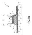
- a typical FBAR-based deviceis shown in FIGS. 1 a and 1 b.
- the FBAR devicecomprises a substrate 110 , a bottom electrode 120 , a piezoelectric layer 130 , and a top electrode 140 .
- the FBAR devicemay additionally include a membrane layer 112 and a sacrificial layer 114 , among others.
- the substratecan be made from silicon (Si), silicon dioxide (SiO2), Gallium Arsenide (GaAs), glass or ceramic materials.
- the bottom electrode and top electrodecan be made from gold (Au), molybdenum (Mo), tungsten (W), copper (Cu), nickel (Ni), titanium (Ti), Niobium (Nb), silver (Ag), tantalum (Ta), cobalt (Co), or aluminum (Al).
- the piezoelectric layer 130can be made from zinc oxide (ZnO), zinc sulfide (ZnS), aluminum nitride (AlN), lithium tantalate (LiTaO 3 ) or other members of the so-called lead lanthanum zirconate titanate family.
- the passivation layeris typically made from a dielectric material, such as SiO2, Si3N4, or polyimide, to serve as an electrical insulator and to protect the piezoelectric layer.
- a dielectric materialsuch as SiO2, Si3N4, or polyimide
- the sacrificial layer 114 in a bridge-type BAW deviceis, in general, etched away in the final fabrication stages to create an air interface beneath the device.
- a mirror-type BAW devicethere is an acoustic mirror structure beneath the bottom electrode 120 .
- the mirror structureconsists of several layer pairs of high and low acoustic impedance materials, usually quarter-wave thick.
- the bridge-type and the mirror-type BAW devicesare known in the art.
- the desired electrical response in an FBAR-based deviceis achieved by a shear or longitudinal acoustic wave propagating in the vertical thickness through the device. Besides these wave modes, there exist other modes, including other shear modes, extensional modes and their higher harmonics. However, with respect to the operation point, the Lamb wave modes in the nearby frequencies are the unwanted spurious modes that may deteriorate the electrical response. In quartz crystals, the strength of these spurious modes is controlled by adjusting the thickness and the width of the top electrode. In an FBAR-based device, the dimension in thickness direction is so small that it renders thickness adjustment difficult and impractical. A possible solution to resolving the problems associated with the spurious modes is to thicken the edge of the top electrode. As disclosed in Kaitila et al.
- a frame-like structure 150is formed on top of the top electrode 140 to thicken the edge thereof.
- the frame-like structure 150is a rectangular frame for defining a first zone and a second zone for acoustic wave excitation.
- the first zoneis the area under the frame-like structure 150
- the second zone 148is the area surrounded by the frame-like structure 150 .
- a Smith Chartis a polar plot of the complex reflection, which represents the ratio of the complex amplitudes of the backward and forward waves.
- the Smith Charthelps translating the reflection coefficient into impedance, and it maps part of the impedance plane onto a unit circle.
- the piston modeis a vibration mode where the vibration amplitude is practically uniform over the second zone. If a resonator exhibits the piston mode, the spurious modes become very weakly excited and the response of the resonator is optimized with respect to the spurious resonances.
- the Smith Chartshows a clean circle, the structure of the resonator is close to a piston mode producing structure.
- the Smith Chartis a good indicator of the quality of the resonator response.
- the outermost circle that touches the square frame of the plotis the unit circle in the Smith Chart.
- the frame-like structuremay be circular, square, polygonal, regular or irregular.
- the frame-like structurecan have different configurations, as shown in FIGS. 2 and 3, to achieve the piston mode.
- part of the piezoelectric layer 130is covered by a passivation layer 160 , and part of the passivation layer is sandwiched between the piezoelectric layer 130 and the frame-like structure 150 extended upward from the edge of the top electrode 140 .
- the frame-like structure 150is basically where the top electrode 140 overlaps with the passivation layer 130 .
- FIG. 1 ais a cross sectional view of a BAW device, as viewed in the lateral direction
- FIG. 2 and FIG. 3are cross sectional views of a BAW device, as viewed in the horizontal direction.
- the frequency of the shunt resonatorsIn FBAR-based ladder filters, the frequency of the shunt resonators must be down-shifted by adding an extra thin-film of a suitable material to the film stack of the resonator.
- the added thin-filmis usually referred to as the tuning layer.
- the thickness of the tuning layeris determined by the desired frequency shift and is generally much smaller than the thickness of other layers on the device. If the shunt resonator in a ladder filter is designed to operate optimally, with regard to the suppression of the spurious mode without the tuning layer, adding the tuning layer may degrade the performance of the resonator by re-introducing the spurious resonance frequencies.
- This objectcan be achieved by configuring the tuning layer.
- a method of tuning a bulk acoustic wave devicecomprising a substrate and a plurality of acoustic wave generating and controlling layers formed on the substrate, wherein the acoustic wave generating and controlling layers include a piezoelectric layer formed between a first electrode and a second electrode for generating piezoelectrically excited acoustic signals, wherein the first electrode has a frame-like structure at an edge portion of the first electrode for reducing spurious resonance components in the acoustic waves, and the frame-like structure surrounds a center zone having a surface area, and wherein the device has a resonance frequency which can be down-shifted by modifying the first electrode.
- the methodcomprises the step of providing a tuning layer on top of the first electrode for modifying the first electrode such that the tuning layer covers at least the surface area of the center zone for reducing spurious resonance resulting from the tuning layer.
- the tuning layeralso covers at least part of the frame-like structure.
- the tuning layersubstantially covers the entire frame-like structure.
- a bulk acoustic wave devicecomprising a substrate and a plurality of acoustic wave generating and controlling layers formed on the substrate, wherein the acoustic wave generating and controlling layers include a piezoelectric layer formed between a first electrode and a second electrode for generating piezoelectrically excited acoustic signals, wherein the first electrode has a frame-like structure at an edge portion of the first electrode for reducing spurious resonance components in the acoustic signals and the frame-like structure surrounds a center zone having a surface area, and wherein the device has a resonance frequency which can be down-shifted by modifying the first electrode.
- the devicecomprises a tuning layer provided on top of the first electrode for modifying the first electrode such that the tuning layer covers at least the surface area of the center zone, and alternatively, at least part of the frame-like structure as well as the surface area of the center zone.
- the tuning layersubstantially covers the entire frame-like structure as well as the surface area of the center zone.
- FIG. 1 ais a cross sectional view illustrating a bulk acoustic wave device having a top electrode with a thickened edge or frame-like structure provided thereon for reducing spurious resonance.
- FIG. 1 bis a top view of the bulk acoustic wave device as shown in FIG. 1 a.
- FIG. 2is a cross sectional view illustrating another bulk acoustic wave device having a frame-like structure on top of the top electrode.
- FIG. 3is a cross sectional view illustrating yet another bulk acoustic wave device havina frame-like structure on top of the top electrode.
- FIG. 4is a Smith Chart showing the effect of the frame-like structure on the electrical response of the bulk acoustic wave device.
- FIG. 5is a cross sectional view showing a tuning layer used for frequency down-shifting a bulk acoustic wave device, wherein the surface area of the tuning layer is smaller than the surface area of the center zone.
- FIG. 6 ais a cross sectional view showing a bulk acoustic wave device having a tuning layer, according to the present invention.
- FIG. 6 bis a cross sectional view showing a bulk acoustic wave device having a tuning layer, according to another embodiment of the present invention.
- FIG. 6 cis a cross sectional view showing a bulk acoustic wave device having a tuning layer, according to the preferred embodiment of the present invention.
- FIG. 7 ais a Smith Chart showing the electrical response of a bulk acoustic wave device including spurious resonance components due to the tuning layer, wherein the gap between the tuning layer and the frame-like structure is about 2.4% of the entire width of the resonator.
- FIG. 7 bis a Smith Chart showing the reduction of spurious resonance by extending the tuning layer toward the frame-like structure, such that the gap between the tuning layer and the frame-like structure is about 1.7% of the entire width of the resonator.
- FIG. 7 cis a Smith Chart showing the reduction of spurious resonance by further extending tuning layer toward the frame-like structure, such that the gap between the tuning layer and the frame-like structure is about 0.7% of the entire width of the resonator.
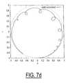
- FIG. 7 dis a Smith Chart showing the reduction of spurious resonance by further extending the tuning layer to cover the entire center area.
- FIG. 7 eis a Smith Chart showing the reduction of spurious resonance by extending the tuning layer to cover part of the frame-like structure.
- FIG. 7 fis a Smith Chart showing the reduction of spurious resonance by extending the tuning layer to cover the entire frame-like structure.
- FIG. 8 ais a cross sectional view showing a variation of the preferred embodiment of the present invention.
- FIG. 8 bis a cross sectional view showing yet another variation of the preferred embodiment of the present invention.
- FIG. 9is a Smith Chart showing the electrical response of a frame-tuned resonator where the frame-like structure in shunt resonators is designed such that a tuning layer is considered as part of the resonators, and the electrical response of an optimally tuned resonator.
- FIG. 5shows a bulk acoustic wave device 10 formed on a substrate 20 and having a piezoelectric layer 24 sandwiched between a bottom electrode 22 and a top electrode 26 for generating piezoelectrically excited acoustic signals.
- the top electrode 26has a frame-like structure 30 surrounding a center zone 28 for reducing spurious components in the acoustic signals.
- the surface area of the center zone 28as surrounded by the frame-like structure 30 , is denoted by SC.
- the surface area of the frame-like structureis denoted by SF.
- a tuning layer 32having a thickness TT and a surface area ST, is provided on top of the top electrode 26 for down-shifting the frequency of the device 10 .
- the thickness TTis related to the amount of frequency down-shifting. It has been found that, when the surface area ST of the tuning layer 32 is smaller than the surface area SC, leaving a gap G, the electrical response of the device 10 shows a substantial amount of spurious resonance, as shown in FIG. 7 a. Thus, the addition of the tuning layer 32 on top of the top electrode 26 introduces spurious resonance components to the piezoelectrically excited acoustic signals.
- FIG. 7 ashows the spurious resonance when the gap G between the tuning layer 32 and the frame-like structure 30 is about 2.4% of the width of the device.
- the bulk acoustic wave device 12 ′has a tuning layer 34 which has an extended section 34 ′ to overlap partially with the frame-like structure 30 .
- the overlapped width of the extended section 34 ′is denoted by letter L.
- the spurious resonancebecomes insignificant.
- the device 12 ′′represents one form of the preferred embodiment of the present invention. Other forms of the preferred embodiment of the present invention are shown in FIGS. 8 a and 8 b.
- the transition from the center zone 28 to the frame-like structure 30 of the top electrode 26is less abrupt than that in the device 12 ′′, as shown in FIG. 6 c. Accordingly, the transition from the tuning layer 34 to the extended section 34 ′ is less abrupt than its counterpart on the device 12 ′′, as shown in FIG. 6 c.
- the frame-like structure 30is a thickened edge of the top electrode 26 . Accordingly, the extended section 34 ′ is formed on top of the thickened edge 30 .
- the method of reducing spurious resonance in the electrical response due to frequency down-shiftinghas been described in conjunction with a number of simple bulk acoustic wave devices as illustrated in FIGS. 6 a , 6 b, 6 c, 8 a and 8 b.
- FIGS. 6 a , 6 b, 6 c, 8 a and 8 bthere are only three acoustic-wave generating and controlling layers, namely, the top electrode, the piezoelectric layer and the bottom electrode.
- the same methodcan also be used on more complex bulk acoustic wave devices having additional acoustic-wave generating and controlling layers.
- the tuning layer as described in conjunction with FIGS. 6 a- 6 c, 8 a and 8 bis concerned with the top electrode of a BAW device.
- the tuning layeris positioned below the piezoelectric layer or below the bottom electrode. In either case, the tuning layer should laterally extend over all of the center area and most of the frame-like structure area. Furthermore, if the tuning layer is positioned between the piezoelectric layer and the bottom electrode, it is preferred to use an electrically conductive tuning layer so that the tuning layer forms part of the bottom electrode.
- the tuning layercan be made from the same material as the top electrode, but it can also be made from a different material.
- the top electrodeis made of aluminum
- the tuning layercan be made of aluminum, molybdenum, tungsten, copper, gold or other electrically conductive material.
- the tuning layercan be made of a non-electrically conductive material such as SiO2, Si3N4, and the like.
- the critical points in selecting the tuning materialare the etch selectivity against other layers for the patterning process and the ability to accurately deposit the correct thickness of the tuning layer. In general, it is preferable to use a lighter material for the tuning layer because a thicker layer would be needed for the same frequency shift. Precise deposition of a thinner layer is generally more difficult than that of a thicker layer.
- the tuning layer 34 ′ and the top electrode 30are made of the same material, as shown in FIGS. 6 c and 8 a, together they appear to be the same as the top electrode 140 , as shown in FIGS. 2 and 3.
- the shunt resonatorsIn a device that consists of series and shunt resonators, the shunt resonators always require some kind of tuning.
- the frame-like area of the shunt resonatorscould be different from that of the series resonators.
- the frame-like area of the tuned resonatorscould also be different from that of the series resonators.
- the dimensions of the frame-like structure on the top electrode, according to Kaitilaare calculated based on a set of boundary conditions. If the frame-like structure in shunt resonators is designed according to Kaitila and considering the tuning layer as a part of the resonator in the first place, the dimension of the frame-like structure in these frame-tuned resonators would be slightly different from the frame-like structure that reproduces the piston mode.
- the electrical response of a frame-tuned resonator(solid line) is shown in FIG. 9 .
- the non-circularityis about 0.11%.
- the width of the frame-like structurecan be modified to reproduce the piston mode (dashed line), as shown in FIG. 9 .
- the bulk acoustic wave devicesinclude individual resonators, stacked crystal filters, ladder filters and the combinations thereof.
- filter typesin addition to the ladder structure that can be constructed from FBARs. All of them include some resonators, which have to be tuned, but they cannot be called parallel or shunt resonators in all cases.
- the balanced filteris an example of such a filter type.
Landscapes
- Engineering & Computer Science (AREA)
- Manufacturing & Machinery (AREA)
- Piezo-Electric Or Mechanical Vibrators, Or Delay Or Filter Circuits (AREA)
- Surface Acoustic Wave Elements And Circuit Networks Thereof (AREA)
Abstract
Description
Claims (9)
Priority Applications (4)
| Application Number | Priority Date | Filing Date | Title |
|---|---|---|---|
| US09/845,089US6476536B1 (en) | 2001-04-27 | 2001-04-27 | Method of tuning BAW resonators |
| EP02008095AEP1258989B1 (en) | 2001-04-27 | 2002-04-11 | Method of tuning baw resonators |
| AT02008095TATE397320T1 (en) | 2001-04-27 | 2002-04-11 | METHOD FOR TUNING ACOUSTIC VOLUME WAVE RESONATORS |
| DE60226805TDE60226805D1 (en) | 2001-04-27 | 2002-04-11 | Method for tuning bulk acoustic wave resonators |
Applications Claiming Priority (1)
| Application Number | Priority Date | Filing Date | Title |
|---|---|---|---|
| US09/845,089US6476536B1 (en) | 2001-04-27 | 2001-04-27 | Method of tuning BAW resonators |
Publications (2)
| Publication Number | Publication Date |
|---|---|
| US20020158716A1 US20020158716A1 (en) | 2002-10-31 |
| US6476536B1true US6476536B1 (en) | 2002-11-05 |
Family
ID=25294358
Family Applications (1)
| Application Number | Title | Priority Date | Filing Date |
|---|---|---|---|
| US09/845,089Expired - LifetimeUS6476536B1 (en) | 2001-04-27 | 2001-04-27 | Method of tuning BAW resonators |
Country Status (4)
| Country | Link |
|---|---|
| US (1) | US6476536B1 (en) |
| EP (1) | EP1258989B1 (en) |
| AT (1) | ATE397320T1 (en) |
| DE (1) | DE60226805D1 (en) |
Cited By (75)
| Publication number | Priority date | Publication date | Assignee | Title |
|---|---|---|---|---|
| US20020149300A1 (en)* | 2001-04-12 | 2002-10-17 | Jyrki Kaitila | Method of producting thin-film acoustic wave devices |
| US20040140868A1 (en)* | 2002-06-11 | 2004-07-22 | Murata Manufacturing Co., Ltd. | Piezoelectric thin-film resonator, piezoelectric filter, and electronic component including the piezoelectric filter |
| US20040145272A1 (en)* | 2003-01-29 | 2004-07-29 | Shim Dong S. | Tuning of packaged film bulk acoustic resonator filters |
| US6812619B1 (en)* | 1999-07-19 | 2004-11-02 | Nokia Corporation | Resonator structure and a filter comprising such a resonator structure |
| US20050029907A1 (en)* | 2001-11-05 | 2005-02-10 | Matsushita Elec. Ind. Co. Ltd. | A method of manufacturing a thin film piezoelectric element |
| US20050134406A1 (en)* | 2003-11-25 | 2005-06-23 | Tdk Corporation | Piezoelectric thin film resonator and method for manufacturing the same |
| US20050140247A1 (en)* | 2003-12-26 | 2005-06-30 | Lee Joo H. | Film bulk acoustic wave resonator device and manufacturing method thereof |
| US20050151600A1 (en)* | 2002-05-23 | 2005-07-14 | Masaki Takeuchi | Piezoelectric thin-film resonator, piezoelectric filter, and electronic component including the piezoelectric filter |
| US20050275486A1 (en)* | 2004-06-14 | 2005-12-15 | Hongiun Feng | Acoustic resonator performance enhancements using recessed region |
| US20060059269A1 (en)* | 2004-09-13 | 2006-03-16 | Chien Chen | Transparent recovery of switch device |
| US20060071736A1 (en)* | 2004-10-01 | 2006-04-06 | Ruby Richard C | Acoustic resonator performance enhancement using alternating frame structure |
| US20060091978A1 (en)* | 2004-11-03 | 2006-05-04 | Kun Wang | Acoustically coupled thin-film resonators |
| US20060128058A1 (en)* | 2004-12-15 | 2006-06-15 | Dungan Thomas E | Wafer bonding of micro-electro mechanical systems to active circuitry |
| US20070007853A1 (en)* | 2005-07-09 | 2007-01-11 | Toit Nicolaas D | Apparatus and method capable of a high fundamental acoustic resonance frequency and a wide resonance-free frequency range |
| US20070090085A1 (en)* | 2001-08-27 | 2007-04-26 | Matsushita Electric Industrial Co., Ltd. | Piezoelectric device and method of manufacturing the device |
| US7332985B2 (en) | 2003-10-30 | 2008-02-19 | Avago Technologies Wireless Ip (Singapore) Pte Ltd. | Cavity-less film bulk acoustic resonator (FBAR) devices |
| US7362198B2 (en) | 2003-10-30 | 2008-04-22 | Avago Technologies Wireless Ip (Singapore) Pte. Ltd | Pass bandwidth control in decoupled stacked bulk acoustic resonator devices |
| US7367095B2 (en) | 2003-10-30 | 2008-05-06 | Avago Technologies General Ip Pte Ltd | Method of making an acoustically coupled transformer |
| US7369013B2 (en) | 2005-04-06 | 2008-05-06 | Avago Technologies Wireless Ip Pte Ltd | Acoustic resonator performance enhancement using filled recessed region |
| US7388455B2 (en) | 2003-10-30 | 2008-06-17 | Avago Technologies Wireless Ip Pte Ltd | Film acoustically-coupled transformer with increased common mode rejection |
| US7391286B2 (en) | 2005-10-06 | 2008-06-24 | Avago Wireless Ip Pte Ltd | Impedance matching and parasitic capacitor resonance of FBAR resonators and coupled filters |
| US20080169885A1 (en)* | 2007-01-11 | 2008-07-17 | Fujitsu Media Devices Limited | Piezoelectric thin-film resonator, acoustic wave device and method for fabricating the acoustic wave device |
| US20080179991A1 (en)* | 2006-04-28 | 2008-07-31 | Murata Manufacturing Co., Ltd. | Electronic component and manufacturing method thereof |
| US7423503B2 (en) | 2005-10-18 | 2008-09-09 | Avago Technologies Wireless Ip (Singapore) Pte. Ltd. | Acoustic galvanic isolator incorporating film acoustically-coupled transformer |
| US7425787B2 (en) | 2005-10-18 | 2008-09-16 | Avago Technologies Wireless Ip (Singapore) Pte. Ltd. | Acoustic galvanic isolator incorporating single insulated decoupled stacked bulk acoustic resonator with acoustically-resonant electrical insulator |
| US7424772B2 (en) | 2003-10-30 | 2008-09-16 | Avago Technologies Wireless Ip (Singapore) Pte. Ltd. | Stacked bulk acoustic resonator band-pass filter with controllable pass bandwidth |
| US7427819B2 (en) | 2005-03-04 | 2008-09-23 | Avago Wireless Ip Pte Ltd | Film-bulk acoustic wave resonator with motion plate and method |
| US7436269B2 (en) | 2005-04-18 | 2008-10-14 | Avago Technologies Wireless Ip (Singapore) Pte. Ltd. | Acoustically coupled resonators and method of making the same |
| US7463499B2 (en) | 2005-10-31 | 2008-12-09 | Avago Technologies General Ip (Singapore) Pte Ltd. | AC-DC power converter |
| US7479685B2 (en) | 2006-03-10 | 2009-01-20 | Avago Technologies General Ip (Singapore) Pte. Ltd. | Electronic device on substrate with cavity and mitigated parasitic leakage path |
| US20090033177A1 (en)* | 2005-08-08 | 2009-02-05 | Kabushiki Kaisha Toshiba | Thin film piezoelectric resonator and method of manufacturing the same |
| US7508286B2 (en) | 2006-09-28 | 2009-03-24 | Avago Technologies Wireless Ip (Singapore) Pte. Ltd. | HBAR oscillator and method of manufacture |
| US7525398B2 (en) | 2005-10-18 | 2009-04-28 | Avago Technologies General Ip (Singapore) Pte. Ltd. | Acoustically communicating data signals across an electrical isolation barrier |
| US7561009B2 (en) | 2005-11-30 | 2009-07-14 | Avago Technologies General Ip (Singapore) Pte. Ltd. | Film bulk acoustic resonator (FBAR) devices with temperature compensation |
| US7612636B2 (en) | 2006-01-30 | 2009-11-03 | Avago Technologies Wireless Ip (Singapore) Pte. Ltd. | Impedance transforming bulk acoustic wave baluns |
| US7615833B2 (en) | 2004-07-13 | 2009-11-10 | Avago Technologies Wireless Ip (Singapore) Pte. Ltd. | Film bulk acoustic resonator package and method of fabricating same |
| US7629865B2 (en) | 2006-05-31 | 2009-12-08 | Avago Technologies Wireless Ip (Singapore) Pte. Ltd. | Piezoelectric resonator structures and electrical filters |
| US20100033055A1 (en)* | 2008-08-11 | 2010-02-11 | Fujitsu Limited | Method for manufacturing elastic wave device |
| US7675390B2 (en) | 2005-10-18 | 2010-03-09 | Avago Technologies Wireless Ip (Singapore) Pte. Ltd. | Acoustic galvanic isolator incorporating single decoupled stacked bulk acoustic resonator |
| US7732977B2 (en) | 2008-04-30 | 2010-06-08 | Avago Technologies Wireless Ip (Singapore) | Transceiver circuit for film bulk acoustic resonator (FBAR) transducers |
| US7737807B2 (en) | 2005-10-18 | 2010-06-15 | Avago Technologies Wireless Ip (Singapore) Pte. Ltd. | Acoustic galvanic isolator incorporating series-connected decoupled stacked bulk acoustic resonators |
| US7746677B2 (en) | 2006-03-09 | 2010-06-29 | Avago Technologies Wireless Ip (Singapore) Pte. Ltd. | AC-DC converter circuit and power supply |
| US7791435B2 (en) | 2007-09-28 | 2010-09-07 | Avago Technologies Wireless Ip (Singapore) Pte. Ltd. | Single stack coupled resonators having differential output |
| US7791434B2 (en) | 2004-12-22 | 2010-09-07 | Avago Technologies Wireless Ip (Singapore) Pte. Ltd. | Acoustic resonator performance enhancement using selective metal etch and having a trench in the piezoelectric |
| US7802349B2 (en) | 2003-03-07 | 2010-09-28 | Avago Technologies Wireless Ip (Singapore) Pte. Ltd. | Manufacturing process for thin film bulk acoustic resonator (FBAR) filters |
| US7855618B2 (en) | 2008-04-30 | 2010-12-21 | Avago Technologies Wireless Ip (Singapore) Pte. Ltd. | Bulk acoustic resonator electrical impedance transformers |
| USRE42009E1 (en)* | 2003-09-17 | 2010-12-28 | Panasonic Corporation | Piezoelectric resonator having a spurious component control layer, filter using the piezoelectric resonator, and duplexer using the piezoelectric resonator |
| US7868522B2 (en) | 2005-09-09 | 2011-01-11 | Avago Technologies Wireless Ip (Singapore) Pte. Ltd. | Adjusted frequency temperature coefficient resonator |
| US8193877B2 (en) | 2009-11-30 | 2012-06-05 | Avago Technologies Wireless Ip (Singapore) Pte. Ltd. | Duplexer with negative phase shifting circuit |
| US8248185B2 (en) | 2009-06-24 | 2012-08-21 | Avago Technologies Wireless Ip (Singapore) Pte. Ltd. | Acoustic resonator structure comprising a bridge |
| US8350445B1 (en) | 2011-06-16 | 2013-01-08 | Avago Technologies Wireless Ip (Singapore) Pte. Ltd. | Bulk acoustic resonator comprising non-piezoelectric layer and bridge |
| US8575820B2 (en) | 2011-03-29 | 2013-11-05 | Avago Technologies General Ip (Singapore) Pte. Ltd. | Stacked bulk acoustic resonator |
| US20140118087A1 (en)* | 2012-10-29 | 2014-05-01 | Avago Technologies General Ip (Singapore) Pte. Ltd. | Acoustic resonator comprising collar and frame |
| US8796904B2 (en) | 2011-10-31 | 2014-08-05 | Avago Technologies General Ip (Singapore) Pte. Ltd. | Bulk acoustic resonator comprising piezoelectric layer and inverse piezoelectric layer |
| US8902023B2 (en) | 2009-06-24 | 2014-12-02 | Avago Technologies General Ip (Singapore) Pte. Ltd. | Acoustic resonator structure having an electrode with a cantilevered portion |
| US8910355B2 (en) | 2011-12-12 | 2014-12-16 | International Business Machines Corporation | Method of manufacturing a film bulk acoustic resonator with a loading element |
| US8922302B2 (en) | 2011-08-24 | 2014-12-30 | Avago Technologies General Ip (Singapore) Pte. Ltd. | Acoustic resonator formed on a pedestal |
| US8962443B2 (en) | 2011-01-31 | 2015-02-24 | Avago Technologies General Ip (Singapore) Pte. Ltd. | Semiconductor device having an airbridge and method of fabricating the same |
| US8981876B2 (en) | 2004-11-15 | 2015-03-17 | Avago Technologies General Ip (Singapore) Pte. Ltd. | Piezoelectric resonator structures and electrical filters having frame elements |
| US9048812B2 (en) | 2011-02-28 | 2015-06-02 | Avago Technologies General Ip (Singapore) Pte. Ltd. | Bulk acoustic wave resonator comprising bridge formed within piezoelectric layer |
| US9083302B2 (en) | 2011-02-28 | 2015-07-14 | Avago Technologies General Ip (Singapore) Pte. Ltd. | Stacked bulk acoustic resonator comprising a bridge and an acoustic reflector along a perimeter of the resonator |
| US9136818B2 (en) | 2011-02-28 | 2015-09-15 | Avago Technologies General Ip (Singapore) Pte. Ltd. | Stacked acoustic resonator comprising a bridge |
| US9148117B2 (en) | 2011-02-28 | 2015-09-29 | Avago Technologies General Ip (Singapore) Pte. Ltd. | Coupled resonator filter comprising a bridge and frame elements |
| US9154112B2 (en) | 2011-02-28 | 2015-10-06 | Avago Technologies General Ip (Singapore) Pte. Ltd. | Coupled resonator filter comprising a bridge |
| US9203374B2 (en) | 2011-02-28 | 2015-12-01 | Avago Technologies General Ip (Singapore) Pte. Ltd. | Film bulk acoustic resonator comprising a bridge |
| US9243316B2 (en) | 2010-01-22 | 2016-01-26 | Avago Technologies General Ip (Singapore) Pte. Ltd. | Method of fabricating piezoelectric material with selected c-axis orientation |
| US9425764B2 (en) | 2012-10-25 | 2016-08-23 | Avago Technologies General Ip (Singapore) Pte. Ltd. | Accoustic resonator having composite electrodes with integrated lateral features |
| US9444426B2 (en) | 2012-10-25 | 2016-09-13 | Avago Technologies General Ip (Singapore) Pte. Ltd. | Accoustic resonator having integrated lateral feature and temperature compensation feature |
| US9490418B2 (en) | 2011-03-29 | 2016-11-08 | Avago Technologies General Ip (Singapore) Pte. Ltd. | Acoustic resonator comprising collar and acoustic reflector with temperature compensating layer |
| US9590165B2 (en) | 2011-03-29 | 2017-03-07 | Avago Technologies General Ip (Singapore) Pte. Ltd. | Acoustic resonator comprising aluminum scandium nitride and temperature compensation feature |
| US10476469B2 (en) | 2016-02-17 | 2019-11-12 | Board of Trustees of the Univsity of Illinois | Spurious-mode-free, laterally-vibrating microelectromechanical system resonators |
| US10873316B2 (en) | 2017-03-02 | 2020-12-22 | Samsung Electro-Mechanics Co., Ltd. | Acoustic resonator and method of manufacturing the same |
| US11082023B2 (en) | 2018-09-24 | 2021-08-03 | Skyworks Global Pte. Ltd. | Multi-layer raised frame in bulk acoustic wave device |
| US11581869B2 (en) | 2020-09-30 | 2023-02-14 | Skyworks Global Pte. Ltd. | Bulk acoustic wave resonator with mass loading layer |
| US12101077B2 (en) | 2020-09-18 | 2024-09-24 | Skyworks Global Pte. Ltd. | Bulk acoustic wave device with raised frame structure |
Families Citing this family (17)
| Publication number | Priority date | Publication date | Assignee | Title |
|---|---|---|---|---|
| TWI365603B (en)* | 2004-10-01 | 2012-06-01 | Avago Technologies Wireless Ip | A thin film bulk acoustic resonator with a mass loaded perimeter |
| US7280007B2 (en) | 2004-11-15 | 2007-10-09 | Avago Technologies General Ip (Singapore) Pte. Ltd. | Thin film bulk acoustic resonator with a mass loaded perimeter |
| EP1944866B1 (en)* | 2005-11-04 | 2011-12-28 | Murata Manufacturing Co., Ltd. | Piezoelectric thin film resonator |
| US9673778B2 (en) | 2009-06-24 | 2017-06-06 | Avago Technologies General Ip (Singapore) Pte. Ltd. | Solid mount bulk acoustic wave resonator structure comprising a bridge |
| US20120326807A1 (en)* | 2009-06-24 | 2012-12-27 | Avago Technologies Wireless Ip (Singapore) Pte. Ltd. | Acoustic resonator structure having an electrode with a cantilevered portion |
| US9520856B2 (en) | 2009-06-24 | 2016-12-13 | Avago Technologies General Ip (Singapore) Pte. Ltd. | Acoustic resonator structure having an electrode with a cantilevered portion |
| US9450561B2 (en) | 2009-11-25 | 2016-09-20 | Avago Technologies General Ip (Singapore) Pte. Ltd. | Bulk acoustic wave (BAW) resonator structure having an electrode with a cantilevered portion and a piezoelectric layer with varying amounts of dopant |
| US9219464B2 (en) | 2009-11-25 | 2015-12-22 | Avago Technologies General Ip (Singapore) Pte. Ltd. | Bulk acoustic wave (BAW) resonator structure having an electrode with a cantilevered portion and a piezoelectric layer with multiple dopants |
| US8384497B2 (en)* | 2009-12-18 | 2013-02-26 | Hao Zhang | Piezoelectric resonator structure having an interference structure |
| US8791776B2 (en)* | 2011-01-19 | 2014-07-29 | Wei Pang | Acoustic wave resonator having a gasket |
| US9099983B2 (en) | 2011-02-28 | 2015-08-04 | Avago Technologies General Ip (Singapore) Pte. Ltd. | Bulk acoustic wave resonator device comprising a bridge in an acoustic reflector |
| US9608592B2 (en) | 2014-01-21 | 2017-03-28 | Avago Technologies General Ip (Singapore) Pte. Ltd. | Film bulk acoustic wave resonator (FBAR) having stress-relief |
| KR20170141386A (en)* | 2016-06-15 | 2017-12-26 | 삼성전기주식회사 | Acoustic wave filter device |
| US10833646B2 (en)* | 2016-10-12 | 2020-11-10 | Samsung Electro-Mechanics Co., Ltd. | Bulk-acoustic wave resonator and method for manufacturing the same |
| DE102018125498B4 (en)* | 2018-10-15 | 2020-04-23 | RF360 Europe GmbH | Electroacoustic RF filter with improved performance and multiplexer component that includes an RF filter |
| CN115242215B (en)* | 2022-09-19 | 2023-02-21 | 常州承芯半导体有限公司 | Bulk acoustic wave resonator device and method of forming the same |
| CN118100840A (en)* | 2024-03-11 | 2024-05-28 | 睿思微系统(烟台)有限公司 | A method for preparing a bulk acoustic wave resonator and a bulk acoustic wave resonator |
Citations (9)
| Publication number | Priority date | Publication date | Assignee | Title |
|---|---|---|---|---|
| US4211947A (en)* | 1977-02-09 | 1980-07-08 | Kabushiki Kaisha Seikosha | Thickness-shear mode quartz oscillator with an added non-circular mass |
| US5714917A (en)* | 1996-10-02 | 1998-02-03 | Nokia Mobile Phones Limited | Device incorporating a tunable thin film bulk acoustic resonator for performing amplitude and phase modulation |
| US5789845A (en)* | 1994-11-24 | 1998-08-04 | Mitsubishi Denki Kabushiki Kaisha | Film bulk acoustic wave device |
| US5880552A (en)* | 1997-05-27 | 1999-03-09 | The United States Of America As Represented By The Secretary Of The Navy | Diamond or diamond like carbon coated chemical sensors and a method of making same |
| US6081171A (en) | 1998-04-08 | 2000-06-27 | Nokia Mobile Phones Limited | Monolithic filters utilizing thin film bulk acoustic wave devices and minimum passive components for controlling the shape and width of a passband response |
| US6111341A (en)* | 1997-02-26 | 2000-08-29 | Toyo Communication Equipment Co., Ltd. | Piezoelectric vibrator and method for manufacturing the same |
| WO2001006647A1 (en) | 1999-07-19 | 2001-01-25 | Nokia Corporation | Resonator structure and a filter comprising such a resonator structure |
| US6307447B1 (en)* | 1999-11-01 | 2001-10-23 | Agere Systems Guardian Corp. | Tuning mechanical resonators for electrical filter |
| US20020014808A1 (en)* | 1998-01-16 | 2002-02-07 | Koichiro Misu | Thin film pietoelectric element |
Family Cites Families (3)
| Publication number | Priority date | Publication date | Assignee | Title |
|---|---|---|---|---|
| DE1566009A1 (en)* | 1967-08-26 | 1971-02-18 | Telefunken Patent | Mechanical frequency filter and method of its manufacture |
| US6051907A (en)* | 1996-10-10 | 2000-04-18 | Nokia Mobile Phones Limited | Method for performing on-wafer tuning of thin film bulk acoustic wave resonators (FBARS) |
| US5780713A (en)* | 1996-11-19 | 1998-07-14 | Hewlett-Packard Company | Post-fabrication tuning of acoustic resonators |
- 2001
- 2001-04-27USUS09/845,089patent/US6476536B1/ennot_activeExpired - Lifetime
- 2002
- 2002-04-11DEDE60226805Tpatent/DE60226805D1/ennot_activeExpired - Lifetime
- 2002-04-11EPEP02008095Apatent/EP1258989B1/ennot_activeExpired - Lifetime
- 2002-04-11ATAT02008095Tpatent/ATE397320T1/ennot_activeIP Right Cessation
Patent Citations (9)
| Publication number | Priority date | Publication date | Assignee | Title |
|---|---|---|---|---|
| US4211947A (en)* | 1977-02-09 | 1980-07-08 | Kabushiki Kaisha Seikosha | Thickness-shear mode quartz oscillator with an added non-circular mass |
| US5789845A (en)* | 1994-11-24 | 1998-08-04 | Mitsubishi Denki Kabushiki Kaisha | Film bulk acoustic wave device |
| US5714917A (en)* | 1996-10-02 | 1998-02-03 | Nokia Mobile Phones Limited | Device incorporating a tunable thin film bulk acoustic resonator for performing amplitude and phase modulation |
| US6111341A (en)* | 1997-02-26 | 2000-08-29 | Toyo Communication Equipment Co., Ltd. | Piezoelectric vibrator and method for manufacturing the same |
| US5880552A (en)* | 1997-05-27 | 1999-03-09 | The United States Of America As Represented By The Secretary Of The Navy | Diamond or diamond like carbon coated chemical sensors and a method of making same |
| US20020014808A1 (en)* | 1998-01-16 | 2002-02-07 | Koichiro Misu | Thin film pietoelectric element |
| US6081171A (en) | 1998-04-08 | 2000-06-27 | Nokia Mobile Phones Limited | Monolithic filters utilizing thin film bulk acoustic wave devices and minimum passive components for controlling the shape and width of a passband response |
| WO2001006647A1 (en) | 1999-07-19 | 2001-01-25 | Nokia Corporation | Resonator structure and a filter comprising such a resonator structure |
| US6307447B1 (en)* | 1999-11-01 | 2001-10-23 | Agere Systems Guardian Corp. | Tuning mechanical resonators for electrical filter |
Cited By (111)
| Publication number | Priority date | Publication date | Assignee | Title |
|---|---|---|---|---|
| US6812619B1 (en)* | 1999-07-19 | 2004-11-02 | Nokia Corporation | Resonator structure and a filter comprising such a resonator structure |
| US6548943B2 (en)* | 2001-04-12 | 2003-04-15 | Nokia Mobile Phones Ltd. | Method of producing thin-film bulk acoustic wave devices |
| US20020149300A1 (en)* | 2001-04-12 | 2002-10-17 | Jyrki Kaitila | Method of producting thin-film acoustic wave devices |
| US20070090085A1 (en)* | 2001-08-27 | 2007-04-26 | Matsushita Electric Industrial Co., Ltd. | Piezoelectric device and method of manufacturing the device |
| US7380320B2 (en)* | 2001-08-27 | 2008-06-03 | Matsushita Electric Industrial Co., Ltd. | Piezoelectric device and method of manufacturing the device |
| US20050029907A1 (en)* | 2001-11-05 | 2005-02-10 | Matsushita Elec. Ind. Co. Ltd. | A method of manufacturing a thin film piezoelectric element |
| US6903497B2 (en)* | 2001-11-05 | 2005-06-07 | Matsushita Electric Industrial Co., Ltd. | Thin film piezoelectric element |
| US7276994B2 (en) | 2002-05-23 | 2007-10-02 | Murata Manufacturing Co., Ltd. | Piezoelectric thin-film resonator, piezoelectric filter, and electronic component including the piezoelectric filter |
| US20050151600A1 (en)* | 2002-05-23 | 2005-07-14 | Masaki Takeuchi | Piezoelectric thin-film resonator, piezoelectric filter, and electronic component including the piezoelectric filter |
| US7002437B2 (en)* | 2002-06-11 | 2006-02-21 | Murata Manufacturing Co., Ltd. | Piezoelectric thin-film resonator, piezoelectric filter, and electronic component including the piezoelectric filter |
| US20040140868A1 (en)* | 2002-06-11 | 2004-07-22 | Murata Manufacturing Co., Ltd. | Piezoelectric thin-film resonator, piezoelectric filter, and electronic component including the piezoelectric filter |
| US20040145272A1 (en)* | 2003-01-29 | 2004-07-29 | Shim Dong S. | Tuning of packaged film bulk acoustic resonator filters |
| US6787970B2 (en)* | 2003-01-29 | 2004-09-07 | Intel Corporation | Tuning of packaged film bulk acoustic resonator filters |
| US7802349B2 (en) | 2003-03-07 | 2010-09-28 | Avago Technologies Wireless Ip (Singapore) Pte. Ltd. | Manufacturing process for thin film bulk acoustic resonator (FBAR) filters |
| USRE42009E1 (en)* | 2003-09-17 | 2010-12-28 | Panasonic Corporation | Piezoelectric resonator having a spurious component control layer, filter using the piezoelectric resonator, and duplexer using the piezoelectric resonator |
| US7400217B2 (en) | 2003-10-30 | 2008-07-15 | Avago Technologies Wireless Ip Pte Ltd | Decoupled stacked bulk acoustic resonator band-pass filter with controllable pass bandwith |
| US7362198B2 (en) | 2003-10-30 | 2008-04-22 | Avago Technologies Wireless Ip (Singapore) Pte. Ltd | Pass bandwidth control in decoupled stacked bulk acoustic resonator devices |
| US7388455B2 (en) | 2003-10-30 | 2008-06-17 | Avago Technologies Wireless Ip Pte Ltd | Film acoustically-coupled transformer with increased common mode rejection |
| US7367095B2 (en) | 2003-10-30 | 2008-05-06 | Avago Technologies General Ip Pte Ltd | Method of making an acoustically coupled transformer |
| US7391285B2 (en) | 2003-10-30 | 2008-06-24 | Avago Technologies Wireless Ip Pte Ltd | Film acoustically-coupled transformer |
| US7358831B2 (en) | 2003-10-30 | 2008-04-15 | Avago Technologies Wireless Ip (Singapore) Pte. Ltd. | Film bulk acoustic resonator (FBAR) devices with simplified packaging |
| US7424772B2 (en) | 2003-10-30 | 2008-09-16 | Avago Technologies Wireless Ip (Singapore) Pte. Ltd. | Stacked bulk acoustic resonator band-pass filter with controllable pass bandwidth |
| US7408428B2 (en) | 2003-10-30 | 2008-08-05 | Avago Technologies Wireless Ip (Singapore) Pte. Ltd. | Temperature-compensated film bulk acoustic resonator (FBAR) devices |
| US7332985B2 (en) | 2003-10-30 | 2008-02-19 | Avago Technologies Wireless Ip (Singapore) Pte Ltd. | Cavity-less film bulk acoustic resonator (FBAR) devices |
| US20050134406A1 (en)* | 2003-11-25 | 2005-06-23 | Tdk Corporation | Piezoelectric thin film resonator and method for manufacturing the same |
| US20050140247A1 (en)* | 2003-12-26 | 2005-06-30 | Lee Joo H. | Film bulk acoustic wave resonator device and manufacturing method thereof |
| US20050275486A1 (en)* | 2004-06-14 | 2005-12-15 | Hongiun Feng | Acoustic resonator performance enhancements using recessed region |
| US7161448B2 (en) | 2004-06-14 | 2007-01-09 | Avago Technologies Wireless Ip (Singapore) Pte. Ltd. | Acoustic resonator performance enhancements using recessed region |
| US7615833B2 (en) | 2004-07-13 | 2009-11-10 | Avago Technologies Wireless Ip (Singapore) Pte. Ltd. | Film bulk acoustic resonator package and method of fabricating same |
| US20060059269A1 (en)* | 2004-09-13 | 2006-03-16 | Chien Chen | Transparent recovery of switch device |
| US7388454B2 (en) | 2004-10-01 | 2008-06-17 | Avago Technologies Wireless Ip Pte Ltd | Acoustic resonator performance enhancement using alternating frame structure |
| US7714684B2 (en) | 2004-10-01 | 2010-05-11 | Avago Technologies Wireless Ip (Singapore) Pte. Ltd. | Acoustic resonator performance enhancement using alternating frame structure |
| US20060071736A1 (en)* | 2004-10-01 | 2006-04-06 | Ruby Richard C | Acoustic resonator performance enhancement using alternating frame structure |
| US20060091978A1 (en)* | 2004-11-03 | 2006-05-04 | Kun Wang | Acoustically coupled thin-film resonators |
| US7098758B2 (en) | 2004-11-03 | 2006-08-29 | Avago Technologies Wireless Ip (Singapore) Pte. Ltd. | Acoustically coupled thin-film resonators having an electrode with a tapered edge |
| US8981876B2 (en) | 2004-11-15 | 2015-03-17 | Avago Technologies General Ip (Singapore) Pte. Ltd. | Piezoelectric resonator structures and electrical filters having frame elements |
| US20060128058A1 (en)* | 2004-12-15 | 2006-06-15 | Dungan Thomas E | Wafer bonding of micro-electro mechanical systems to active circuitry |
| US8143082B2 (en) | 2004-12-15 | 2012-03-27 | Avago Technologies Wireless Ip (Singapore) Pte. Ltd. | Wafer bonding of micro-electro mechanical systems to active circuitry |
| US7202560B2 (en) | 2004-12-15 | 2007-04-10 | Avago Technologies Wireless Ip (Singapore) Pte. Ltd. | Wafer bonding of micro-electro mechanical systems to active circuitry |
| US8188810B2 (en) | 2004-12-22 | 2012-05-29 | Avago Technologies Wireless Ip (Singapore) Pte. Ltd. | Acoustic resonator performance enhancement using selective metal etch |
| US7791434B2 (en) | 2004-12-22 | 2010-09-07 | Avago Technologies Wireless Ip (Singapore) Pte. Ltd. | Acoustic resonator performance enhancement using selective metal etch and having a trench in the piezoelectric |
| US7427819B2 (en) | 2005-03-04 | 2008-09-23 | Avago Wireless Ip Pte Ltd | Film-bulk acoustic wave resonator with motion plate and method |
| CN1845453B (en)* | 2005-04-06 | 2012-03-07 | 安华高科技无线Ip(新加坡)私人有限公司 | Acoustic resonator and method for manufacturing acoustic resonator |
| US8230562B2 (en) | 2005-04-06 | 2012-07-31 | Avago Technologies Wireless Ip (Singapore) Pte. Ltd. | Method of fabricating an acoustic resonator comprising a filled recessed region |
| US7369013B2 (en) | 2005-04-06 | 2008-05-06 | Avago Technologies Wireless Ip Pte Ltd | Acoustic resonator performance enhancement using filled recessed region |
| US7436269B2 (en) | 2005-04-18 | 2008-10-14 | Avago Technologies Wireless Ip (Singapore) Pte. Ltd. | Acoustically coupled resonators and method of making the same |
| US20070007853A1 (en)* | 2005-07-09 | 2007-01-11 | Toit Nicolaas D | Apparatus and method capable of a high fundamental acoustic resonance frequency and a wide resonance-free frequency range |
| US7709999B2 (en)* | 2005-08-08 | 2010-05-04 | Kabushiki Kaisha Toshiba | Thin film piezoelectric resonator and method of manufacturing the same |
| US20090033177A1 (en)* | 2005-08-08 | 2009-02-05 | Kabushiki Kaisha Toshiba | Thin film piezoelectric resonator and method of manufacturing the same |
| US7868522B2 (en) | 2005-09-09 | 2011-01-11 | Avago Technologies Wireless Ip (Singapore) Pte. Ltd. | Adjusted frequency temperature coefficient resonator |
| US7391286B2 (en) | 2005-10-06 | 2008-06-24 | Avago Wireless Ip Pte Ltd | Impedance matching and parasitic capacitor resonance of FBAR resonators and coupled filters |
| US7423503B2 (en) | 2005-10-18 | 2008-09-09 | Avago Technologies Wireless Ip (Singapore) Pte. Ltd. | Acoustic galvanic isolator incorporating film acoustically-coupled transformer |
| US7425787B2 (en) | 2005-10-18 | 2008-09-16 | Avago Technologies Wireless Ip (Singapore) Pte. Ltd. | Acoustic galvanic isolator incorporating single insulated decoupled stacked bulk acoustic resonator with acoustically-resonant electrical insulator |
| US7675390B2 (en) | 2005-10-18 | 2010-03-09 | Avago Technologies Wireless Ip (Singapore) Pte. Ltd. | Acoustic galvanic isolator incorporating single decoupled stacked bulk acoustic resonator |
| US7525398B2 (en) | 2005-10-18 | 2009-04-28 | Avago Technologies General Ip (Singapore) Pte. Ltd. | Acoustically communicating data signals across an electrical isolation barrier |
| US7737807B2 (en) | 2005-10-18 | 2010-06-15 | Avago Technologies Wireless Ip (Singapore) Pte. Ltd. | Acoustic galvanic isolator incorporating series-connected decoupled stacked bulk acoustic resonators |
| US7463499B2 (en) | 2005-10-31 | 2008-12-09 | Avago Technologies General Ip (Singapore) Pte Ltd. | AC-DC power converter |
| US7852644B2 (en) | 2005-10-31 | 2010-12-14 | Avago Technologies General Ip (Singapore) Pte. Ltd. | AC-DC power converter |
| US7561009B2 (en) | 2005-11-30 | 2009-07-14 | Avago Technologies General Ip (Singapore) Pte. Ltd. | Film bulk acoustic resonator (FBAR) devices with temperature compensation |
| US7612636B2 (en) | 2006-01-30 | 2009-11-03 | Avago Technologies Wireless Ip (Singapore) Pte. Ltd. | Impedance transforming bulk acoustic wave baluns |
| US7746677B2 (en) | 2006-03-09 | 2010-06-29 | Avago Technologies Wireless Ip (Singapore) Pte. Ltd. | AC-DC converter circuit and power supply |
| US8238129B2 (en) | 2006-03-09 | 2012-08-07 | Avago Technologies Wireless Ip (Singapore) Pte. Ltd. | AC-DC converter circuit and power supply |
| US8080854B2 (en) | 2006-03-10 | 2011-12-20 | Avago Technologies General Ip (Singapore) Pte. Ltd. | Electronic device on substrate with cavity and mitigated parasitic leakage path |
| US7479685B2 (en) | 2006-03-10 | 2009-01-20 | Avago Technologies General Ip (Singapore) Pte. Ltd. | Electronic device on substrate with cavity and mitigated parasitic leakage path |
| US20080179991A1 (en)* | 2006-04-28 | 2008-07-31 | Murata Manufacturing Co., Ltd. | Electronic component and manufacturing method thereof |
| US7541722B2 (en)* | 2006-04-28 | 2009-06-02 | Murata Manufacturing Co., Ltd. | Electronic component and manufacturing method thereof |
| US7629865B2 (en) | 2006-05-31 | 2009-12-08 | Avago Technologies Wireless Ip (Singapore) Pte. Ltd. | Piezoelectric resonator structures and electrical filters |
| US7508286B2 (en) | 2006-09-28 | 2009-03-24 | Avago Technologies Wireless Ip (Singapore) Pte. Ltd. | HBAR oscillator and method of manufacture |
| US20080169885A1 (en)* | 2007-01-11 | 2008-07-17 | Fujitsu Media Devices Limited | Piezoelectric thin-film resonator, acoustic wave device and method for fabricating the acoustic wave device |
| US7791435B2 (en) | 2007-09-28 | 2010-09-07 | Avago Technologies Wireless Ip (Singapore) Pte. Ltd. | Single stack coupled resonators having differential output |
| US7732977B2 (en) | 2008-04-30 | 2010-06-08 | Avago Technologies Wireless Ip (Singapore) | Transceiver circuit for film bulk acoustic resonator (FBAR) transducers |
| US7855618B2 (en) | 2008-04-30 | 2010-12-21 | Avago Technologies Wireless Ip (Singapore) Pte. Ltd. | Bulk acoustic resonator electrical impedance transformers |
| US20100033055A1 (en)* | 2008-08-11 | 2010-02-11 | Fujitsu Limited | Method for manufacturing elastic wave device |
| US8186030B2 (en)* | 2008-08-11 | 2012-05-29 | Taiyo Yuden Co., Ltd. | Method for manufacturing elastic wave device |
| US8902023B2 (en) | 2009-06-24 | 2014-12-02 | Avago Technologies General Ip (Singapore) Pte. Ltd. | Acoustic resonator structure having an electrode with a cantilevered portion |
| US8248185B2 (en) | 2009-06-24 | 2012-08-21 | Avago Technologies Wireless Ip (Singapore) Pte. Ltd. | Acoustic resonator structure comprising a bridge |
| US8193877B2 (en) | 2009-11-30 | 2012-06-05 | Avago Technologies Wireless Ip (Singapore) Pte. Ltd. | Duplexer with negative phase shifting circuit |
| US9243316B2 (en) | 2010-01-22 | 2016-01-26 | Avago Technologies General Ip (Singapore) Pte. Ltd. | Method of fabricating piezoelectric material with selected c-axis orientation |
| US9859205B2 (en) | 2011-01-31 | 2018-01-02 | Avago Technologies General Ip (Singapore) Pte. Ltd. | Semiconductor device having an airbridge and method of fabricating the same |
| US8962443B2 (en) | 2011-01-31 | 2015-02-24 | Avago Technologies General Ip (Singapore) Pte. Ltd. | Semiconductor device having an airbridge and method of fabricating the same |
| US9148117B2 (en) | 2011-02-28 | 2015-09-29 | Avago Technologies General Ip (Singapore) Pte. Ltd. | Coupled resonator filter comprising a bridge and frame elements |
| US9203374B2 (en) | 2011-02-28 | 2015-12-01 | Avago Technologies General Ip (Singapore) Pte. Ltd. | Film bulk acoustic resonator comprising a bridge |
| US9048812B2 (en) | 2011-02-28 | 2015-06-02 | Avago Technologies General Ip (Singapore) Pte. Ltd. | Bulk acoustic wave resonator comprising bridge formed within piezoelectric layer |
| US9154112B2 (en) | 2011-02-28 | 2015-10-06 | Avago Technologies General Ip (Singapore) Pte. Ltd. | Coupled resonator filter comprising a bridge |
| US9136818B2 (en) | 2011-02-28 | 2015-09-15 | Avago Technologies General Ip (Singapore) Pte. Ltd. | Stacked acoustic resonator comprising a bridge |
| US9083302B2 (en) | 2011-02-28 | 2015-07-14 | Avago Technologies General Ip (Singapore) Pte. Ltd. | Stacked bulk acoustic resonator comprising a bridge and an acoustic reflector along a perimeter of the resonator |
| US9590165B2 (en) | 2011-03-29 | 2017-03-07 | Avago Technologies General Ip (Singapore) Pte. Ltd. | Acoustic resonator comprising aluminum scandium nitride and temperature compensation feature |
| US8575820B2 (en) | 2011-03-29 | 2013-11-05 | Avago Technologies General Ip (Singapore) Pte. Ltd. | Stacked bulk acoustic resonator |
| US9490418B2 (en) | 2011-03-29 | 2016-11-08 | Avago Technologies General Ip (Singapore) Pte. Ltd. | Acoustic resonator comprising collar and acoustic reflector with temperature compensating layer |
| US8350445B1 (en) | 2011-06-16 | 2013-01-08 | Avago Technologies Wireless Ip (Singapore) Pte. Ltd. | Bulk acoustic resonator comprising non-piezoelectric layer and bridge |
| US8922302B2 (en) | 2011-08-24 | 2014-12-30 | Avago Technologies General Ip (Singapore) Pte. Ltd. | Acoustic resonator formed on a pedestal |
| US8796904B2 (en) | 2011-10-31 | 2014-08-05 | Avago Technologies General Ip (Singapore) Pte. Ltd. | Bulk acoustic resonator comprising piezoelectric layer and inverse piezoelectric layer |
| US8910355B2 (en) | 2011-12-12 | 2014-12-16 | International Business Machines Corporation | Method of manufacturing a film bulk acoustic resonator with a loading element |
| US9444426B2 (en) | 2012-10-25 | 2016-09-13 | Avago Technologies General Ip (Singapore) Pte. Ltd. | Accoustic resonator having integrated lateral feature and temperature compensation feature |
| US9425764B2 (en) | 2012-10-25 | 2016-08-23 | Avago Technologies General Ip (Singapore) Pte. Ltd. | Accoustic resonator having composite electrodes with integrated lateral features |
| US9490771B2 (en)* | 2012-10-29 | 2016-11-08 | Avago Technologies General Ip (Singapore) Pte. Ltd. | Acoustic resonator comprising collar and frame |
| US20140118087A1 (en)* | 2012-10-29 | 2014-05-01 | Avago Technologies General Ip (Singapore) Pte. Ltd. | Acoustic resonator comprising collar and frame |
| US11496110B2 (en) | 2016-02-17 | 2022-11-08 | The Board Of Trustees Of The University Of Illinois | Spurious-mode-free, laterally-vibrating microelectromechanical system resonators |
| US10476469B2 (en) | 2016-02-17 | 2019-11-12 | Board of Trustees of the Univsity of Illinois | Spurious-mode-free, laterally-vibrating microelectromechanical system resonators |
| US10873316B2 (en) | 2017-03-02 | 2020-12-22 | Samsung Electro-Mechanics Co., Ltd. | Acoustic resonator and method of manufacturing the same |
| US11082023B2 (en) | 2018-09-24 | 2021-08-03 | Skyworks Global Pte. Ltd. | Multi-layer raised frame in bulk acoustic wave device |
| US11967939B2 (en) | 2018-09-24 | 2024-04-23 | Skyworks Global Pte. Ltd. | Multi-layer raised frame in bulk acoustic wave device |
| US12341486B2 (en) | 2018-09-24 | 2025-06-24 | Skyworks Global Pte. Ltd. | Multi-layer raised frame in bulk acoustic wave device |
| US12278611B2 (en) | 2020-09-18 | 2025-04-15 | Skyworks Global Pte. Ltd. | Multi-gradient raised frame in bulk acoustic wave device |
| US12283937B2 (en)* | 2020-09-18 | 2025-04-22 | Skyworks Global Pte. Ltd. | Bulk acoustic wave device with multi-gradient raised frame |
| US12101077B2 (en) | 2020-09-18 | 2024-09-24 | Skyworks Global Pte. Ltd. | Bulk acoustic wave device with raised frame structure |
| US11581869B2 (en) | 2020-09-30 | 2023-02-14 | Skyworks Global Pte. Ltd. | Bulk acoustic wave resonator with mass loading layer |
| US12088278B2 (en) | 2020-09-30 | 2024-09-10 | Skyworks Global Pte. Ltd. | Bulk acoustic wave resonator with patterned mass loading layer and recessed frame |
| US12021506B2 (en) | 2020-09-30 | 2024-06-25 | Skyworks Global Pte. Ltd. | Bulk acoustic wave resonators with patterned mass loading layers |
| US12368427B2 (en) | 2020-09-30 | 2025-07-22 | Skyworks Global Pte. Ltd. | Bulk acoustic wave resonators with patterned mass loading layers |
| US12381529B2 (en) | 2020-09-30 | 2025-08-05 | Skyworks Global Pte. Ltd. | Methods of manufacturing bulk acoustic wave resonators with patterned mass loading layers |
Also Published As
| Publication number | Publication date |
|---|---|
| US20020158716A1 (en) | 2002-10-31 |
| DE60226805D1 (en) | 2008-07-10 |
| EP1258989B1 (en) | 2008-05-28 |
| EP1258989A2 (en) | 2002-11-20 |
| EP1258989A3 (en) | 2004-01-28 |
| ATE397320T1 (en) | 2008-06-15 |
Similar Documents
| Publication | Publication Date | Title |
|---|---|---|
| US6476536B1 (en) | Method of tuning BAW resonators | |
| CN110011637B (en) | Elastic wave device | |
| KR100698985B1 (en) | Filter and manufacturing method | |
| EP1196989B1 (en) | Resonator structure and a filter having such a resonator structure | |
| US6107721A (en) | Piezoelectric resonators on a differentially offset reflector | |
| US7138889B2 (en) | Single-port multi-resonator acoustic resonator device | |
| KR100901954B1 (en) | Bulk acoustic wave resonator with two piezoelectric layers as a balun in filters and duplexers | |
| US7522018B2 (en) | Electro-acoustic resonator with a top electrode layer thinner than a bottom electrode layer | |
| US6924717B2 (en) | Tapered electrode in an acoustic resonator | |
| US10218335B2 (en) | Duplexer | |
| US10958239B2 (en) | Bulk acoustic wave resonator | |
| US7649304B2 (en) | Piezoelectric resonator and piezoelectric filter | |
| KR100771345B1 (en) | Piezoelectric thin-film resonator and filter | |
| US20100134210A1 (en) | Piezoelectric Resonator and Piezoelectric Filter Device | |
| US10164601B2 (en) | BAW resonator having temperature compensation | |
| US20040021400A1 (en) | Resonator with seed layer | |
| JP2018182463A (en) | Piezoelectric thin film resonator, filter and multiplexer | |
| US20150130560A1 (en) | Piezoelectric thin-film resonator, filter and duplexer | |
| JP5128077B2 (en) | Thin film piezoelectric resonator and thin film piezoelectric filter using the same | |
| US20190074817A1 (en) | Baw resonator less prone to spurious modes, baw filter, and manufacturing method | |
| KR20250090634A (en) | Bulk acoustic wave resonator |
Legal Events
| Date | Code | Title | Description |
|---|---|---|---|
| AS | Assignment | Owner name:NOKIA CORPORATION, FINLAND Free format text:ASSIGNMENT OF ASSIGNORS INTEREST;ASSIGNOR:PENSALA, TUOMAS;REEL/FRAME:011969/0551 Effective date:20010520 | |
| STCF | Information on status: patent grant | Free format text:PATENTED CASE | |
| FPAY | Fee payment | Year of fee payment:4 | |
| AS | Assignment | Owner name:AVAGO TECHNOLOGIES WIRELESS IP (SINGAPORE) PTE. LT Free format text:ASSIGNMENT OF ASSIGNORS INTEREST;ASSIGNOR:NOKIA CORPORATION;REEL/FRAME:021118/0874 Effective date:20071107 | |
| FPAY | Fee payment | Year of fee payment:8 | |
| AS | Assignment | Owner name:AVAGO TECHNOLOGIES GENERAL IP (SINGAPORE) PTE. LTD Free format text:MERGER;ASSIGNOR:AVAGO TECHNOLOGIES WIRELESS IP (SINGAPORE) PTE. LTD.;REEL/FRAME:030369/0703 Effective date:20121030 | |
| FPAY | Fee payment | Year of fee payment:12 | |
| AS | Assignment | Owner name:DEUTSCHE BANK AG NEW YORK BRANCH, AS COLLATERAL AGENT, NEW YORK Free format text:PATENT SECURITY AGREEMENT;ASSIGNOR:AVAGO TECHNOLOGIES GENERAL IP (SINGAPORE) PTE. LTD.;REEL/FRAME:032851/0001 Effective date:20140506 Owner name:DEUTSCHE BANK AG NEW YORK BRANCH, AS COLLATERAL AG Free format text:PATENT SECURITY AGREEMENT;ASSIGNOR:AVAGO TECHNOLOGIES GENERAL IP (SINGAPORE) PTE. LTD.;REEL/FRAME:032851/0001 Effective date:20140506 | |
| AS | Assignment | Owner name:AVAGO TECHNOLOGIES GENERAL IP (SINGAPORE) PTE. LTD., SINGAPORE Free format text:TERMINATION AND RELEASE OF SECURITY INTEREST IN PATENT RIGHTS (RELEASES RF 032851-0001);ASSIGNOR:DEUTSCHE BANK AG NEW YORK BRANCH, AS COLLATERAL AGENT;REEL/FRAME:037689/0001 Effective date:20160201 Owner name:AVAGO TECHNOLOGIES GENERAL IP (SINGAPORE) PTE. LTD Free format text:TERMINATION AND RELEASE OF SECURITY INTEREST IN PATENT RIGHTS (RELEASES RF 032851-0001);ASSIGNOR:DEUTSCHE BANK AG NEW YORK BRANCH, AS COLLATERAL AGENT;REEL/FRAME:037689/0001 Effective date:20160201 | |
| AS | Assignment | Owner name:BANK OF AMERICA, N.A., AS COLLATERAL AGENT, NORTH CAROLINA Free format text:PATENT SECURITY AGREEMENT;ASSIGNOR:AVAGO TECHNOLOGIES GENERAL IP (SINGAPORE) PTE. LTD.;REEL/FRAME:037808/0001 Effective date:20160201 Owner name:BANK OF AMERICA, N.A., AS COLLATERAL AGENT, NORTH Free format text:PATENT SECURITY AGREEMENT;ASSIGNOR:AVAGO TECHNOLOGIES GENERAL IP (SINGAPORE) PTE. LTD.;REEL/FRAME:037808/0001 Effective date:20160201 | |
| AS | Assignment | Owner name:AVAGO TECHNOLOGIES GENERAL IP (SINGAPORE) PTE. LTD., SINGAPORE Free format text:TERMINATION AND RELEASE OF SECURITY INTEREST IN PATENTS;ASSIGNOR:BANK OF AMERICA, N.A., AS COLLATERAL AGENT;REEL/FRAME:041710/0001 Effective date:20170119 Owner name:AVAGO TECHNOLOGIES GENERAL IP (SINGAPORE) PTE. LTD Free format text:TERMINATION AND RELEASE OF SECURITY INTEREST IN PATENTS;ASSIGNOR:BANK OF AMERICA, N.A., AS COLLATERAL AGENT;REEL/FRAME:041710/0001 Effective date:20170119 | |
| AS | Assignment | Owner name:AVAGO TECHNOLOGIES INTERNATIONAL SALES PTE. LIMITE Free format text:MERGER;ASSIGNOR:AVAGO TECHNOLOGIES GENERAL IP (SINGAPORE) PTE. LTD.;REEL/FRAME:047195/0026 Effective date:20180509 | |
| AS | Assignment | Owner name:AVAGO TECHNOLOGIES INTERNATIONAL SALES PTE. LIMITE Free format text:CORRECTIVE ASSIGNMENT TO CORRECT THE EFFECTIVE DATE OF MERGER PREVIOUSLY RECORDED ON REEL 047195 FRAME 0026. ASSIGNOR(S) HEREBY CONFIRMS THE MERGER;ASSIGNOR:AVAGO TECHNOLOGIES GENERAL IP (SINGAPORE) PTE. LTD.;REEL/FRAME:047477/0423 Effective date:20180905 |