US6475646B2 - Lead frame and method of manufacturing the lead frame - Google Patents
Lead frame and method of manufacturing the lead frameDownload PDFInfo
- Publication number
- US6475646B2 US6475646B2US09/731,766US73176600AUS6475646B2US 6475646 B2US6475646 B2US 6475646B2US 73176600 AUS73176600 AUS 73176600AUS 6475646 B2US6475646 B2US 6475646B2
- Authority
- US
- United States
- Prior art keywords
- thin plate
- plate material
- lead frame
- inclusions
- degreasing
- Prior art date
- Legal status (The legal status is an assumption and is not a legal conclusion. Google has not performed a legal analysis and makes no representation as to the accuracy of the status listed.)
- Expired - Lifetime, expires
Links
Images


Classifications
- B—PERFORMING OPERATIONS; TRANSPORTING
- B32—LAYERED PRODUCTS
- B32B—LAYERED PRODUCTS, i.e. PRODUCTS BUILT-UP OF STRATA OF FLAT OR NON-FLAT, e.g. CELLULAR OR HONEYCOMB, FORM
- B32B15/00—Layered products comprising a layer of metal
- B—PERFORMING OPERATIONS; TRANSPORTING
- B32—LAYERED PRODUCTS
- B32B—LAYERED PRODUCTS, i.e. PRODUCTS BUILT-UP OF STRATA OF FLAT OR NON-FLAT, e.g. CELLULAR OR HONEYCOMB, FORM
- B32B15/00—Layered products comprising a layer of metal
- B32B15/01—Layered products comprising a layer of metal all layers being exclusively metallic
- B32B15/018—Layered products comprising a layer of metal all layers being exclusively metallic one layer being formed of a noble metal or a noble metal alloy
- C—CHEMISTRY; METALLURGY
- C25—ELECTROLYTIC OR ELECTROPHORETIC PROCESSES; APPARATUS THEREFOR
- C25D—PROCESSES FOR THE ELECTROLYTIC OR ELECTROPHORETIC PRODUCTION OF COATINGS; ELECTROFORMING; APPARATUS THEREFOR
- C25D5/00—Electroplating characterised by the process; Pretreatment or after-treatment of workpieces
- C25D5/34—Pretreatment of metallic surfaces to be electroplated
- H—ELECTRICITY
- H01—ELECTRIC ELEMENTS
- H01L—SEMICONDUCTOR DEVICES NOT COVERED BY CLASS H10
- H01L21/00—Processes or apparatus adapted for the manufacture or treatment of semiconductor or solid state devices or of parts thereof
- H01L21/02—Manufacture or treatment of semiconductor devices or of parts thereof
- H01L21/04—Manufacture or treatment of semiconductor devices or of parts thereof the devices having potential barriers, e.g. a PN junction, depletion layer or carrier concentration layer
- H01L21/48—Manufacture or treatment of parts, e.g. containers, prior to assembly of the devices, using processes not provided for in a single one of the groups H01L21/18 - H01L21/326 or H10D48/04 - H10D48/07
- H01L21/4814—Conductive parts
- H01L21/4821—Flat leads, e.g. lead frames with or without insulating supports
- H01L21/4835—Cleaning, e.g. removing of solder
- H—ELECTRICITY
- H01—ELECTRIC ELEMENTS
- H01L—SEMICONDUCTOR DEVICES NOT COVERED BY CLASS H10
- H01L2924/00—Indexing scheme for arrangements or methods for connecting or disconnecting semiconductor or solid-state bodies as covered by H01L24/00
- H01L2924/0001—Technical content checked by a classifier
- H01L2924/0002—Not covered by any one of groups H01L24/00, H01L24/00 and H01L2224/00
- Y—GENERAL TAGGING OF NEW TECHNOLOGICAL DEVELOPMENTS; GENERAL TAGGING OF CROSS-SECTIONAL TECHNOLOGIES SPANNING OVER SEVERAL SECTIONS OF THE IPC; TECHNICAL SUBJECTS COVERED BY FORMER USPC CROSS-REFERENCE ART COLLECTIONS [XRACs] AND DIGESTS
- Y10—TECHNICAL SUBJECTS COVERED BY FORMER USPC
- Y10T—TECHNICAL SUBJECTS COVERED BY FORMER US CLASSIFICATION
- Y10T428/00—Stock material or miscellaneous articles
- Y10T428/12—All metal or with adjacent metals
- Y10T428/12493—Composite; i.e., plural, adjacent, spatially distinct metal components [e.g., layers, joint, etc.]
- Y10T428/12771—Transition metal-base component
- Y10T428/12861—Group VIII or IB metal-base component
- Y10T428/12875—Platinum group metal-base component
- Y—GENERAL TAGGING OF NEW TECHNOLOGICAL DEVELOPMENTS; GENERAL TAGGING OF CROSS-SECTIONAL TECHNOLOGIES SPANNING OVER SEVERAL SECTIONS OF THE IPC; TECHNICAL SUBJECTS COVERED BY FORMER USPC CROSS-REFERENCE ART COLLECTIONS [XRACs] AND DIGESTS
- Y10—TECHNICAL SUBJECTS COVERED BY FORMER USPC
- Y10T—TECHNICAL SUBJECTS COVERED BY FORMER US CLASSIFICATION
- Y10T428/00—Stock material or miscellaneous articles
- Y10T428/12—All metal or with adjacent metals
- Y10T428/12493—Composite; i.e., plural, adjacent, spatially distinct metal components [e.g., layers, joint, etc.]
- Y10T428/12771—Transition metal-base component
- Y10T428/12861—Group VIII or IB metal-base component
- Y10T428/12889—Au-base component
- Y—GENERAL TAGGING OF NEW TECHNOLOGICAL DEVELOPMENTS; GENERAL TAGGING OF CROSS-SECTIONAL TECHNOLOGIES SPANNING OVER SEVERAL SECTIONS OF THE IPC; TECHNICAL SUBJECTS COVERED BY FORMER USPC CROSS-REFERENCE ART COLLECTIONS [XRACs] AND DIGESTS
- Y10—TECHNICAL SUBJECTS COVERED BY FORMER USPC
- Y10T—TECHNICAL SUBJECTS COVERED BY FORMER US CLASSIFICATION
- Y10T428/00—Stock material or miscellaneous articles
- Y10T428/12—All metal or with adjacent metals
- Y10T428/12493—Composite; i.e., plural, adjacent, spatially distinct metal components [e.g., layers, joint, etc.]
- Y10T428/12771—Transition metal-base component
- Y10T428/12861—Group VIII or IB metal-base component
- Y10T428/12903—Cu-base component
- Y10T428/1291—Next to Co-, Cu-, or Ni-base component
- Y—GENERAL TAGGING OF NEW TECHNOLOGICAL DEVELOPMENTS; GENERAL TAGGING OF CROSS-SECTIONAL TECHNOLOGIES SPANNING OVER SEVERAL SECTIONS OF THE IPC; TECHNICAL SUBJECTS COVERED BY FORMER USPC CROSS-REFERENCE ART COLLECTIONS [XRACs] AND DIGESTS
- Y10—TECHNICAL SUBJECTS COVERED BY FORMER USPC
- Y10T—TECHNICAL SUBJECTS COVERED BY FORMER US CLASSIFICATION
- Y10T428/00—Stock material or miscellaneous articles
- Y10T428/12—All metal or with adjacent metals
- Y10T428/12493—Composite; i.e., plural, adjacent, spatially distinct metal components [e.g., layers, joint, etc.]
- Y10T428/12771—Transition metal-base component
- Y10T428/12861—Group VIII or IB metal-base component
- Y10T428/12944—Ni-base component
- Y—GENERAL TAGGING OF NEW TECHNOLOGICAL DEVELOPMENTS; GENERAL TAGGING OF CROSS-SECTIONAL TECHNOLOGIES SPANNING OVER SEVERAL SECTIONS OF THE IPC; TECHNICAL SUBJECTS COVERED BY FORMER USPC CROSS-REFERENCE ART COLLECTIONS [XRACs] AND DIGESTS
- Y10—TECHNICAL SUBJECTS COVERED BY FORMER USPC
- Y10T—TECHNICAL SUBJECTS COVERED BY FORMER US CLASSIFICATION
- Y10T428/00—Stock material or miscellaneous articles
- Y10T428/12—All metal or with adjacent metals
- Y10T428/12993—Surface feature [e.g., rough, mirror]
Definitions
- the present inventionrelates to a semiconductor lead frame, and more particularly, to a lead frame having an improved pre-treatment process and a plating method of the lead frame.
- a semiconductor lead frameis an important element of a semiconductor package, together with semiconductor chips, and connects the inside of the semiconductor package and the outside thereof and supports the semiconductor chips.
- a semiconductor lead frameis generally manufactured by a stamping process or an etching process.
- a semiconductor lead frame manufactured by one of the two processing methodshas a variety of structures according to the type of being mounted on a substrate.
- FIG. 1is a schematic plan view illustrating the structure of a conventional semiconductor lead frame.
- a semiconductor lead frame 10includes a die pad unit 11 for mounting a semiconductor memory chip and fixing the same at a static state, an internal lead 12 connected to the chip by wire bonding, and an external lead 13 for connection with an external circuit.
- the semiconductor lead frame 10 having the aforementioned configurationforms a semiconductor package through assembly with other parts of the semiconductor, e.g., a memory chip.
- a metal material having a predetermined propertyis often plated on the die pad unit 11 and the internal lead 12 of the lead frame 10 .
- solder (Sn—Pb) platingis performed on a predetermined portion of the external lead 13 .
- PFpre-plated frame
- a pretreatment processis performed before plating.
- the pre-treatment processis performed for improving adhesiveness between plating layers by cleaning and flattening the plated surface. If the pre-treatment process is incompletely performed, it sometimes happens that various kinds of defects such as generation of peeling or swelling of a plating layer, non-uniform spots and gloss, roughness of a plating layer, or the generation of pinholes.
- the pre-treatment process for suppressing the generation of the above-described defectsis generally electrocleaning including an organic solvent degreasing step, an inorganic matter degreasing step, an acid submerging step and a rinsing step. Also, in order to increase the surface adhesiveness between a raw material and a plating layer, electroplating is additionally performed after the electrocleaning, thereby activating the surface of the raw material.
- the electroplating processactivates the surface of a base metal to increase an interface bondability between a nickel plated layer and the base metal during nickel plating.
- the manufacture stress of the raw material of a semiconductor lead frame manufactured by rollingis not completely removed even if unwinding is performed, and local microcracks or local stress may exist on the surface of the raw material.
- microcrack portions and stress remainder portionsare plated, the microcrack portions are not completely plated and pores may remain. If the pores are exposed to deteriorating conditions, such as heat applied during a semiconductor manufacturing process, corrosion due to microcracks is expedited. Also, corrosion of raw materials of a lead frame may occur due to internal heat caused by continuous operation of semiconductor circuits. Further, cracks may grow over time by the remaining internal bending stress. Thus, the microcracks remaining on the surface of the base metal are etched by electropolishing, thereby removing the microcracks and the remaining stress portions. In this case, if a protective plating layer deposited on the surface of the base metal is considerably thick, the above-noted problems may be prevented to an extent. However, if the underlying plating and protective plating layer are thick, solder wettability is lowered and cracks may be caused during bending.
- the thus-plated nodulesare weakly bonded at interfaces with underlying metal during bending of the thin plate material, they may be separated from bonding. Also, when a semiconductor device is finally mounted on the surface of a substrate, solder wettability may be lowered due to an aging process applied to a lead frame during the manufacture of the semiconductor device.
- the inclusion present on the surface of the base metalis iron (Fe) as in this embodiment, Fe is oxidized more easily than copper (Cu) which is a main material, due to heat applied during manufacture of the semiconductor device, and the thermal diffusion leads to an upper plating layer to then be diffused to the surface of the plating layer, thereby lowering the solder wettability.
- the plating layermay be peeled from the nodules due to a mechanical shock caused by a capillary or thermal pressure during wire bonding.
- the peeled nodulesare electrodeposited on the head portion of the capillary so that the capillary is severely contaminated or abraded, thereby causing the necessity of replacing capillaries often.
- even the bottom layer of the bonded part of a plated lead framemay be damaged due to the nodules electrodeposited on the capillary.
- this problemhas not been generated by forming a thick multi-layer plated layer even if inclusions remain on the surface of the base metal.
- a nickel platingis formed as an underlying layer and then a protective layer is plated as a functional plating layer.
- a protective plating layerbecomes thicker, a standby time for adhesion between the underlying layer at which solder wetting is actually performed, and the solder, is delayed, thereby lowering solder wettability.
- a Pd plating as a protective layeris generally formed to a thickness of 6 to 7 ⁇ m. In this case, the above-mentioned problem is generated due to the inclusion on the surface of the base metal. In the pre-plating which has been recently in widespread use, increasing the plating layer extremely lowers the commercial availability due to a rise in the price of palladium (Pd) which has been widely used as a protective plating layer.
- a method for manufacturing a lead frameincluding the steps of electrocleaning the surface of a thin plate material, electropolishing the electrocleaned thin plate material, removing inclusions on the surface of the electropolished thin plate material, rinsing the inclusion-removed thin plate material with an acidic solution, and forming multi-plated layers on the rinsed material.
- the inclusion-removing stepincludes the step of anodic-degreasing the thin plate material.
- a lead framehaving an inner lead portion and an outer lead portion formed by electropolishing a cleaned thin plate material, removing inclusion on the surface of the electropolished thin plate material having multi-plated layers, rinsing the same and forming multi-plated layers thereon.
- FIG. 1is a schematic plan view illustrating a general semiconductor lead frame
- FIG. 2is a photograph view showing the state of a surface of a conventional thin plate material after electropolishing
- FIG. 3is a cross-sectional view illustrating the cross section of a material before a pre-treatment process
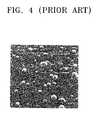
- FIG. 4is a photograph showing the state in which a plating layer is formed on the surface of a thin plate material after electropolishing
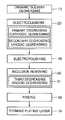
- FIG. 5is a block diagram illustrating the pre-treatment process in a manufacturing method of a lead frame according to the present invention
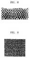
- FIG. 6is a cross-sectional view illustrating the cross section of a material after electropolishing
- FIG. 7shows a photograph of the surface state of a thin plate material after cathodic degreasing and anodic degreasing
- FIG. 8is a cross-sectional view illustrating the cross section of a material after removing inclusions
- FIG. 9shows a photograph in which a plating layer is formed on the surface of the thin plate material shown in FIG. 5;
- FIG. 10shows a photograph of the surface state of a conventional lead frame on which curing and steam-aging are performed after performing multi-layer plating
- FIG. 11shows a photograph of the solder wetting state after performing the steam-aging shown in FIG. 10;
- FIG. 12shows a photograph of the surface of a present invention lead frame on which curing and steam-aging are performed after performing multi-layer plating
- FIG. 13shows a photograph of the solder wetting state after performing the aging shown in FIG. 12 .
- a method of manufacturing a lead frame according to the present inventionrelates to a method of pre-treating a thin plate material for forming the lead frame, and an embodiment thereof is shown in FIG. 5 .
- the pre-treatment process of the present inventionincludes a process of removing oil such as rolling oil or anti-corrosive oil in a raw material.
- the thin plate materialis treated with organic solvent degreasing (step 10 ) and alkali submerging or electrocleaning (step 20 ).
- the electrocleaning (step 20 )may include the sub-steps of primary degreasing (cathodic dereasing), and secondary degreasing (anodic degreasing on cathodic-degreased thin-plate material).
- the electrocleaning (step 20 )may consist of cathodic degreasing only.
- the electrocleaning(step 20 ) is performed by the primary degreasing (cathodic dereasing), and the secondary degreasing (anodic degreasing on anode-degreased thin plate material).
- a current of 90 Ais applied to an electrolytic solution of the electrocleaning step which is an alkaline solution, that is, a 120 g/l of NaOH solution, and then an anode and a cathode are employed to each electrolyte bath by non-contact degreasing.
- a currentis applied to the thin plate material dipped in the alkaline electrolytic solution so that the oil and inorganic matter adhered to the surface of the thin plate material are removed by bubbles generated at the surface.
- compounds on the metal surface or dustare removed by reduction on the metal surface by hydrogens generated on the surface of the thin plate material and oxidation of dust.
- the surface of the electrocleaned thin plate materialis electropolished (step 40 ).
- a mixed solution of phosphoric acid and nitric acidwhich is a 75% acidic solution, is used as an electrolytic solution and a current of 90 A is applied to the thin plate material.
- electropolishingis performed under the above-described circumstances, the surface of the thin plate material is polished in a state in which foreign matter is primarily removed by the cathodic and anodic degreasing.
- remainder Fe noduleswhich are not completely melted with raw materials contained in the thin plate material during preparation of the raw materials, are exposed to the surface of the thin plate material.
- inclusions exposed to the thin plate materialare removed (step 50 ).
- the inclusion removing step (step 50 )includes a third degreasing (anodic degreasing) step (step 51 ).
- the anodic degreasing (step 51 )the thin plate material is employed as an anode and a predetermined metal plate is employed as a cathode to then be immersed in the electrolytic solution.
- the nodules of the thin plate materialare removed by oxidation and anodic dissolution, that is, by charge migration from the anode to the cathode and oxygen generated at the anode.
- a current of 40 Ais applied to 120 g/l of a NaOH solution as the electrolytic solution.
- the components of the inclusions producing after electropolishingmay differ depending on the components of a base metal.
- Si inclusions, rather than Fe nodulesare exposed to the surface of the thin plate material after electropolishing.
- Siis a non-conductive material, they are removed by radiating ultrasonic wave to the surface of the thin plate material, instead of anodic degreasing.
- the thin plate materialis rinsed using an acidic solution to completely wash away foreign matter (step 60 ).
- the inclusion removing stepas described above, the nodules are completely removed from the surface of the thin plate material, as shown in FIGS. 7 and 8.
- multi-plated layers containing protective layersare formed on the thin plate material (step 70 ).
- FIG. 9shows a photograph in which plating layers are formed on the pre-treated thin plate material.
- nodulesare not generated at the surface of the thin plate material, from which it is understood that the roughness of the plating surface has improved.
- nodulescan be prevented from being stripped away from bent portions.
- the plating layerscan be prevented from being peeled off.
- the nodules stripped away from the thin plate materialstick to a head portion of the capillary during wire bonding, thereby preventing the capillary from being severely worn out.
- the lead frame 80 manufactured by the above-described methodincludes internal leads 81 connected to chips by wire bonding, and external leads 82 for being connected to external circuits, as shown in FIG. 1 .
- the lead frame 80 having the aforementioned configurationhas improved surface roughness as nodules are removed from the surface of the material.
- the wearing or contamination of the capillarycan be prevented.
- a problem of poor adhesion between the plating layer and the underlying material (underlying metal), which is a primary cause of impurity in wire bonding,can be fundamentally overcome.
- FIGS. 4 and 9are enlarged views showing the surface states of a conventional lead frame and a lead frame according to the present invention, both being magnified by 3000 times, in which the width and lengths thereof are 40 ⁇ m, that is, the surface area is 1600 ⁇ m 2 and the number of nodules each having a diameter of approximately 1 ⁇ m is noticeably reduced from approximately 50 (prior art) to 0 to 5 (present invention).
- FIGS. 10 through 13show photographs obtained by conducting tests on a lead frame according to the present invention and a conventional lead frame under the conditions applied to a lead frame in a conventional semiconductor manufacturing process.
- FIGS. 10 and 12show photographs of the surface states of a conventional lead frame and a present invention lead frame, on each of which curing is performed at an oven of 175° C. for 2 hours and steam-aging is then performed at 93° C. for 8 hours, after sequentially performing multi-layer plating of nickel and palladium.
- FIGS. 11 and 13show photographs of the solder wetting states of a conventional lead frame and a present invention lead frame, obtained after an R-flux type solder activator is applied to the surfaces of the cured and steam-aged lead frames and the resultant lead frames are dipped into the solder fused at 235° C. for 2 seconds.
- the conventional multi-layer plated lead frame having the inclusions projecting on the surface of the base metalexperiences oxidation around the inclusions while being aged, thereby having low solder wettability.
- the lead frame according to the present inventionhas excellent solder wettability even after being aged, by removing the inclusions remaining on the surface of the base metal.
- the inclusions which may impede solder wettability due to surface mountingare noticeably reduced from the surface, thereby solving the problem of solder wettability.
- the thus manufactured semiconductor lead frame to which pre-plating is applied to a substratehas a protective layer made of precious metal on its outermost layer and intermediate underlying layers.
- the precious metalinclude palladium, palladium alloy, gold, gold alloy and the like.
- a palladium plated layer which is a protective layeris 0.05 to 2 ⁇ m in thickness.
- the thickness of a nickel plated layer which is an underlying layeris 20 to 40 ⁇ m.
- the nodules on the surface of a thin plate materialwhich deteriorate the wire bonding property during the manufacture of a semiconductor device and the solder wettability during surface mounting, are removed during a pre-treatment process, thereby preventing peeling off of a plating layer due to the nodules, generating of cracks, wearing of a capillary due to wire bonding, accumulation of the nodules on the head of the capillary, pressed marks of the plating layer during wire bonding, caused by the nodule accumulation, and so on. Further, the solder wettability of external leads during surface mounting of the lead frame can be improved and cracks due to bending can be prevented.
Landscapes
- Engineering & Computer Science (AREA)
- Chemical & Material Sciences (AREA)
- Condensed Matter Physics & Semiconductors (AREA)
- General Physics & Mathematics (AREA)
- Materials Engineering (AREA)
- Metallurgy (AREA)
- Organic Chemistry (AREA)
- Physics & Mathematics (AREA)
- Chemical Kinetics & Catalysis (AREA)
- Electrochemistry (AREA)
- Manufacturing & Machinery (AREA)
- Computer Hardware Design (AREA)
- Microelectronics & Electronic Packaging (AREA)
- Power Engineering (AREA)
- Lead Frames For Integrated Circuits (AREA)
- Electroplating Methods And Accessories (AREA)
- Cleaning And De-Greasing Of Metallic Materials By Chemical Methods (AREA)
Abstract
Description
Claims (9)
Applications Claiming Priority (5)
| Application Number | Priority Date | Filing Date | Title |
|---|---|---|---|
| KR20000047498 | 2000-08-17 | ||
| KR00-47498 | 2000-08-17 | ||
| KR2000-47498 | 2000-08-17 | ||
| KR10-2000-0068500AKR100378485B1 (en) | 2000-08-17 | 2000-11-17 | Lead frame and method of manufacturing the same |
| KR00-68500 | 2000-11-17 |
Publications (2)
| Publication Number | Publication Date |
|---|---|
| US20020020629A1 US20020020629A1 (en) | 2002-02-21 |
| US6475646B2true US6475646B2 (en) | 2002-11-05 |
Family
ID=26638310
Family Applications (1)
| Application Number | Title | Priority Date | Filing Date |
|---|---|---|---|
| US09/731,766Expired - LifetimeUS6475646B2 (en) | 2000-08-17 | 2000-12-08 | Lead frame and method of manufacturing the lead frame |
Country Status (4)
| Country | Link |
|---|---|
| US (1) | US6475646B2 (en) |
| JP (1) | JP3921341B2 (en) |
| CN (1) | CN1159756C (en) |
| SG (1) | SG87194A1 (en) |
Cited By (41)
| Publication number | Priority date | Publication date | Assignee | Title |
|---|---|---|---|---|
| US7214326B1 (en)* | 2003-11-07 | 2007-05-08 | Amkor Technology, Inc. | Increased capacity leadframe and semiconductor package using the same |
| US20080217186A1 (en)* | 2007-03-09 | 2008-09-11 | Poligrat Gmbh | Electropolishing process for titanium |
| US20080230393A1 (en)* | 2007-03-23 | 2008-09-25 | Fujifilm Corporation | Method and apparatus for producing conductive material |
| US7560804B1 (en) | 1998-06-24 | 2009-07-14 | Amkor Technology, Inc. | Integrated circuit package and method of making the same |
| US7687899B1 (en) | 2007-08-07 | 2010-03-30 | Amkor Technology, Inc. | Dual laminate package structure with embedded elements |
| US7723852B1 (en) | 2008-01-21 | 2010-05-25 | Amkor Technology, Inc. | Stacked semiconductor package and method of making same |
| US7732899B1 (en) | 2005-12-02 | 2010-06-08 | Amkor Technology, Inc. | Etch singulated semiconductor package |
| US7768135B1 (en) | 2008-04-17 | 2010-08-03 | Amkor Technology, Inc. | Semiconductor package with fast power-up cycle and method of making same |
| US7777351B1 (en) | 2007-10-01 | 2010-08-17 | Amkor Technology, Inc. | Thin stacked interposer package |
| US7808084B1 (en) | 2008-05-06 | 2010-10-05 | Amkor Technology, Inc. | Semiconductor package with half-etched locking features |
| US7847392B1 (en) | 2008-09-30 | 2010-12-07 | Amkor Technology, Inc. | Semiconductor device including leadframe with increased I/O |
| US7847386B1 (en) | 2007-11-05 | 2010-12-07 | Amkor Technology, Inc. | Reduced size stacked semiconductor package and method of making the same |
| US7875963B1 (en) | 2008-11-21 | 2011-01-25 | Amkor Technology, Inc. | Semiconductor device including leadframe having power bars and increased I/O |
| US7928542B2 (en) | 2001-03-27 | 2011-04-19 | Amkor Technology, Inc. | Lead frame for semiconductor package |
| US7956453B1 (en) | 2008-01-16 | 2011-06-07 | Amkor Technology, Inc. | Semiconductor package with patterning layer and method of making same |
| US7960818B1 (en) | 2009-03-04 | 2011-06-14 | Amkor Technology, Inc. | Conformal shield on punch QFN semiconductor package |
| US7977774B2 (en) | 2007-07-10 | 2011-07-12 | Amkor Technology, Inc. | Fusion quad flat semiconductor package |
| US7982298B1 (en) | 2008-12-03 | 2011-07-19 | Amkor Technology, Inc. | Package in package semiconductor device |
| US7989933B1 (en) | 2008-10-06 | 2011-08-02 | Amkor Technology, Inc. | Increased I/O leadframe and semiconductor device including same |
| US8008758B1 (en) | 2008-10-27 | 2011-08-30 | Amkor Technology, Inc. | Semiconductor device with increased I/O leadframe |
| US8026589B1 (en) | 2009-02-23 | 2011-09-27 | Amkor Technology, Inc. | Reduced profile stackable semiconductor package |
| US8058715B1 (en) | 2009-01-09 | 2011-11-15 | Amkor Technology, Inc. | Package in package device for RF transceiver module |
| US8067821B1 (en) | 2008-04-10 | 2011-11-29 | Amkor Technology, Inc. | Flat semiconductor package with half package molding |
| US8072050B1 (en) | 2008-11-18 | 2011-12-06 | Amkor Technology, Inc. | Semiconductor device with increased I/O leadframe including passive device |
| US8089159B1 (en) | 2007-10-03 | 2012-01-03 | Amkor Technology, Inc. | Semiconductor package with increased I/O density and method of making the same |
| US8089145B1 (en) | 2008-11-17 | 2012-01-03 | Amkor Technology, Inc. | Semiconductor device including increased capacity leadframe |
| US8125064B1 (en) | 2008-07-28 | 2012-02-28 | Amkor Technology, Inc. | Increased I/O semiconductor package and method of making same |
| US8184453B1 (en) | 2008-07-31 | 2012-05-22 | Amkor Technology, Inc. | Increased capacity semiconductor package |
| US8318287B1 (en) | 1998-06-24 | 2012-11-27 | Amkor Technology, Inc. | Integrated circuit package and method of making the same |
| US8441110B1 (en) | 2006-06-21 | 2013-05-14 | Amkor Technology, Inc. | Side leaded, bottom exposed pad and bottom exposed lead fusion quad flat semiconductor package |
| US8487420B1 (en) | 2008-12-08 | 2013-07-16 | Amkor Technology, Inc. | Package in package semiconductor device with film over wire |
| US8575742B1 (en) | 2009-04-06 | 2013-11-05 | Amkor Technology, Inc. | Semiconductor device with increased I/O leadframe including power bars |
| US8648450B1 (en) | 2011-01-27 | 2014-02-11 | Amkor Technology, Inc. | Semiconductor device including leadframe with a combination of leads and lands |
| US8674485B1 (en) | 2010-12-08 | 2014-03-18 | Amkor Technology, Inc. | Semiconductor device including leadframe with downsets |
| US8680656B1 (en) | 2009-01-05 | 2014-03-25 | Amkor Technology, Inc. | Leadframe structure for concentrated photovoltaic receiver package |
| US9184148B2 (en) | 2013-10-24 | 2015-11-10 | Amkor Technology, Inc. | Semiconductor package and method therefor |
| US9184118B2 (en) | 2013-05-02 | 2015-11-10 | Amkor Technology Inc. | Micro lead frame structure having reinforcing portions and method |
| US9631481B1 (en) | 2011-01-27 | 2017-04-25 | Amkor Technology, Inc. | Semiconductor device including leadframe with a combination of leads and lands and method |
| US9673122B2 (en) | 2014-05-02 | 2017-06-06 | Amkor Technology, Inc. | Micro lead frame structure having reinforcing portions and method |
| US9704725B1 (en) | 2012-03-06 | 2017-07-11 | Amkor Technology, Inc. | Semiconductor device with leadframe configured to facilitate reduced burr formation |
| US10811341B2 (en) | 2009-01-05 | 2020-10-20 | Amkor Technology Singapore Holding Pte Ltd. | Semiconductor device with through-mold via |
Families Citing this family (6)
| Publication number | Priority date | Publication date | Assignee | Title |
|---|---|---|---|---|
| KR20050083322A (en)* | 2004-02-23 | 2005-08-26 | 삼성테크윈 주식회사 | Lead frame for semiconductor package and the fabrication method thereof |
| EP2103712B1 (en)* | 2008-03-20 | 2019-02-13 | ATOTECH Deutschland GmbH | Ni-P layer system and process for its preparation |
| JP5761028B2 (en)* | 2009-12-01 | 2015-08-12 | ニプロ株式会社 | Cell potential measuring container and manufacturing method thereof |
| JP5555146B2 (en) | 2010-12-01 | 2014-07-23 | 株式会社日立製作所 | Metal-resin composite structure and manufacturing method thereof, bus bar, module case, and resin connector part |
| CN107858711A (en)* | 2017-11-28 | 2018-03-30 | 歌尔股份有限公司 | Metallic matrix electro-plating method |
| JP6998761B2 (en)* | 2017-12-26 | 2022-01-18 | 株式会社三井ハイテック | Lead frame manufacturing method |
Citations (8)
| Publication number | Priority date | Publication date | Assignee | Title |
|---|---|---|---|---|
| JPS60225455A (en)* | 1984-04-24 | 1985-11-09 | Kobe Steel Ltd | Lead frame |
| JPH0368788A (en)* | 1989-08-03 | 1991-03-25 | Hitachi Cable Ltd | Production of copper bar for lead frame |
| US5167794A (en)* | 1990-04-16 | 1992-12-01 | Mitsubishi Denki Kabushiki Kaisha | Method for producing lead frame material |
| JPH0866830A (en)* | 1994-08-29 | 1996-03-12 | Sumitomo Metal Mining Co Ltd | Electrolytic polishing method for lead frame made of copper and copper alloy |
| JPH08168924A (en)* | 1994-12-19 | 1996-07-02 | Sumitomo Metal Mining Co Ltd | Electrolytic polishing method and lead frame manufacturing method using the same |
| JPH0964264A (en)* | 1995-08-28 | 1997-03-07 | Dainippon Printing Co Ltd | Lead frame partial plating method |
| US5660708A (en)* | 1994-11-21 | 1997-08-26 | Sumitomo Metal Mining Company, Limited | Process for manufacturing a lead frame |
| JPH10237694A (en)* | 1997-02-24 | 1998-09-08 | Kobe Steel Ltd | Production of copper alloy for lead frame excellent in resin adhesion |
Family Cites Families (2)
| Publication number | Priority date | Publication date | Assignee | Title |
|---|---|---|---|---|
| EP0127857B1 (en)* | 1983-05-28 | 1987-07-29 | Masami Kobayashi | Solderable stainless steel article and method for making same |
| JP2670569B2 (en)* | 1992-07-27 | 1997-10-29 | 株式会社三井ハイテック | Semiconductor device and method of manufacturing lead frame used therefor |
- 2000
- 2000-12-07SGSG200007193Apatent/SG87194A1/enunknown
- 2000-12-08CNCNB001352881Apatent/CN1159756C/ennot_activeExpired - Lifetime
- 2000-12-08USUS09/731,766patent/US6475646B2/ennot_activeExpired - Lifetime
- 2000-12-13JPJP2000378699Apatent/JP3921341B2/ennot_activeExpired - Lifetime
Patent Citations (9)
| Publication number | Priority date | Publication date | Assignee | Title |
|---|---|---|---|---|
| JPS60225455A (en)* | 1984-04-24 | 1985-11-09 | Kobe Steel Ltd | Lead frame |
| JPH0368788A (en)* | 1989-08-03 | 1991-03-25 | Hitachi Cable Ltd | Production of copper bar for lead frame |
| US5167794A (en)* | 1990-04-16 | 1992-12-01 | Mitsubishi Denki Kabushiki Kaisha | Method for producing lead frame material |
| JPH0866830A (en)* | 1994-08-29 | 1996-03-12 | Sumitomo Metal Mining Co Ltd | Electrolytic polishing method for lead frame made of copper and copper alloy |
| US5660708A (en)* | 1994-11-21 | 1997-08-26 | Sumitomo Metal Mining Company, Limited | Process for manufacturing a lead frame |
| US5843290A (en)* | 1994-11-21 | 1998-12-01 | Sumitomo Metal Mining Co., Limited | Electrolytic polishing apparatus |
| JPH08168924A (en)* | 1994-12-19 | 1996-07-02 | Sumitomo Metal Mining Co Ltd | Electrolytic polishing method and lead frame manufacturing method using the same |
| JPH0964264A (en)* | 1995-08-28 | 1997-03-07 | Dainippon Printing Co Ltd | Lead frame partial plating method |
| JPH10237694A (en)* | 1997-02-24 | 1998-09-08 | Kobe Steel Ltd | Production of copper alloy for lead frame excellent in resin adhesion |
Cited By (66)
| Publication number | Priority date | Publication date | Assignee | Title |
|---|---|---|---|---|
| US9224676B1 (en) | 1998-06-24 | 2015-12-29 | Amkor Technology, Inc. | Integrated circuit package and method of making the same |
| US8318287B1 (en) | 1998-06-24 | 2012-11-27 | Amkor Technology, Inc. | Integrated circuit package and method of making the same |
| US8853836B1 (en) | 1998-06-24 | 2014-10-07 | Amkor Technology, Inc. | Integrated circuit package and method of making the same |
| US7560804B1 (en) | 1998-06-24 | 2009-07-14 | Amkor Technology, Inc. | Integrated circuit package and method of making the same |
| US8963301B1 (en) | 1998-06-24 | 2015-02-24 | Amkor Technology, Inc. | Integrated circuit package and method of making the same |
| US7928542B2 (en) | 2001-03-27 | 2011-04-19 | Amkor Technology, Inc. | Lead frame for semiconductor package |
| US8102037B2 (en) | 2001-03-27 | 2012-01-24 | Amkor Technology, Inc. | Leadframe for semiconductor package |
| US7214326B1 (en)* | 2003-11-07 | 2007-05-08 | Amkor Technology, Inc. | Increased capacity leadframe and semiconductor package using the same |
| US7732899B1 (en) | 2005-12-02 | 2010-06-08 | Amkor Technology, Inc. | Etch singulated semiconductor package |
| US8441110B1 (en) | 2006-06-21 | 2013-05-14 | Amkor Technology, Inc. | Side leaded, bottom exposed pad and bottom exposed lead fusion quad flat semiconductor package |
| US20080217186A1 (en)* | 2007-03-09 | 2008-09-11 | Poligrat Gmbh | Electropolishing process for titanium |
| US8133377B2 (en)* | 2007-03-23 | 2012-03-13 | Fujifilm Corporation | Method and apparatus for producing conductive material |
| US20080230393A1 (en)* | 2007-03-23 | 2008-09-25 | Fujifilm Corporation | Method and apparatus for producing conductive material |
| US7977774B2 (en) | 2007-07-10 | 2011-07-12 | Amkor Technology, Inc. | Fusion quad flat semiconductor package |
| US8304866B1 (en) | 2007-07-10 | 2012-11-06 | Amkor Technology, Inc. | Fusion quad flat semiconductor package |
| US7687899B1 (en) | 2007-08-07 | 2010-03-30 | Amkor Technology, Inc. | Dual laminate package structure with embedded elements |
| US7872343B1 (en) | 2007-08-07 | 2011-01-18 | Amkor Technology, Inc. | Dual laminate package structure with embedded elements |
| US8283767B1 (en) | 2007-08-07 | 2012-10-09 | Amkor Technology, Inc. | Dual laminate package structure with embedded elements |
| US8319338B1 (en) | 2007-10-01 | 2012-11-27 | Amkor Technology, Inc. | Thin stacked interposer package |
| US7777351B1 (en) | 2007-10-01 | 2010-08-17 | Amkor Technology, Inc. | Thin stacked interposer package |
| US8089159B1 (en) | 2007-10-03 | 2012-01-03 | Amkor Technology, Inc. | Semiconductor package with increased I/O density and method of making the same |
| US8227921B1 (en) | 2007-10-03 | 2012-07-24 | Amkor Technology, Inc. | Semiconductor package with increased I/O density and method of making same |
| US7847386B1 (en) | 2007-11-05 | 2010-12-07 | Amkor Technology, Inc. | Reduced size stacked semiconductor package and method of making the same |
| US7956453B1 (en) | 2008-01-16 | 2011-06-07 | Amkor Technology, Inc. | Semiconductor package with patterning layer and method of making same |
| US8729710B1 (en) | 2008-01-16 | 2014-05-20 | Amkor Technology, Inc. | Semiconductor package with patterning layer and method of making same |
| US7906855B1 (en) | 2008-01-21 | 2011-03-15 | Amkor Technology, Inc. | Stacked semiconductor package and method of making same |
| US7723852B1 (en) | 2008-01-21 | 2010-05-25 | Amkor Technology, Inc. | Stacked semiconductor package and method of making same |
| US8067821B1 (en) | 2008-04-10 | 2011-11-29 | Amkor Technology, Inc. | Flat semiconductor package with half package molding |
| US8084868B1 (en) | 2008-04-17 | 2011-12-27 | Amkor Technology, Inc. | Semiconductor package with fast power-up cycle and method of making same |
| US7768135B1 (en) | 2008-04-17 | 2010-08-03 | Amkor Technology, Inc. | Semiconductor package with fast power-up cycle and method of making same |
| US7808084B1 (en) | 2008-05-06 | 2010-10-05 | Amkor Technology, Inc. | Semiconductor package with half-etched locking features |
| US8125064B1 (en) | 2008-07-28 | 2012-02-28 | Amkor Technology, Inc. | Increased I/O semiconductor package and method of making same |
| US8184453B1 (en) | 2008-07-31 | 2012-05-22 | Amkor Technology, Inc. | Increased capacity semiconductor package |
| US8299602B1 (en) | 2008-09-30 | 2012-10-30 | Amkor Technology, Inc. | Semiconductor device including leadframe with increased I/O |
| US7847392B1 (en) | 2008-09-30 | 2010-12-07 | Amkor Technology, Inc. | Semiconductor device including leadframe with increased I/O |
| US8432023B1 (en) | 2008-10-06 | 2013-04-30 | Amkor Technology, Inc. | Increased I/O leadframe and semiconductor device including same |
| US7989933B1 (en) | 2008-10-06 | 2011-08-02 | Amkor Technology, Inc. | Increased I/O leadframe and semiconductor device including same |
| US8823152B1 (en) | 2008-10-27 | 2014-09-02 | Amkor Technology, Inc. | Semiconductor device with increased I/O leadframe |
| US8008758B1 (en) | 2008-10-27 | 2011-08-30 | Amkor Technology, Inc. | Semiconductor device with increased I/O leadframe |
| US8089145B1 (en) | 2008-11-17 | 2012-01-03 | Amkor Technology, Inc. | Semiconductor device including increased capacity leadframe |
| US8072050B1 (en) | 2008-11-18 | 2011-12-06 | Amkor Technology, Inc. | Semiconductor device with increased I/O leadframe including passive device |
| US7875963B1 (en) | 2008-11-21 | 2011-01-25 | Amkor Technology, Inc. | Semiconductor device including leadframe having power bars and increased I/O |
| US8188579B1 (en) | 2008-11-21 | 2012-05-29 | Amkor Technology, Inc. | Semiconductor device including leadframe having power bars and increased I/O |
| US7982298B1 (en) | 2008-12-03 | 2011-07-19 | Amkor Technology, Inc. | Package in package semiconductor device |
| US8487420B1 (en) | 2008-12-08 | 2013-07-16 | Amkor Technology, Inc. | Package in package semiconductor device with film over wire |
| US10811341B2 (en) | 2009-01-05 | 2020-10-20 | Amkor Technology Singapore Holding Pte Ltd. | Semiconductor device with through-mold via |
| US11869829B2 (en) | 2009-01-05 | 2024-01-09 | Amkor Technology Singapore Holding Pte. Ltd. | Semiconductor device with through-mold via |
| US8680656B1 (en) | 2009-01-05 | 2014-03-25 | Amkor Technology, Inc. | Leadframe structure for concentrated photovoltaic receiver package |
| US8558365B1 (en) | 2009-01-09 | 2013-10-15 | Amkor Technology, Inc. | Package in package device for RF transceiver module |
| US8058715B1 (en) | 2009-01-09 | 2011-11-15 | Amkor Technology, Inc. | Package in package device for RF transceiver module |
| US8026589B1 (en) | 2009-02-23 | 2011-09-27 | Amkor Technology, Inc. | Reduced profile stackable semiconductor package |
| US8729682B1 (en) | 2009-03-04 | 2014-05-20 | Amkor Technology, Inc. | Conformal shield on punch QFN semiconductor package |
| US7960818B1 (en) | 2009-03-04 | 2011-06-14 | Amkor Technology, Inc. | Conformal shield on punch QFN semiconductor package |
| US8575742B1 (en) | 2009-04-06 | 2013-11-05 | Amkor Technology, Inc. | Semiconductor device with increased I/O leadframe including power bars |
| US8674485B1 (en) | 2010-12-08 | 2014-03-18 | Amkor Technology, Inc. | Semiconductor device including leadframe with downsets |
| US8648450B1 (en) | 2011-01-27 | 2014-02-11 | Amkor Technology, Inc. | Semiconductor device including leadframe with a combination of leads and lands |
| US9275939B1 (en) | 2011-01-27 | 2016-03-01 | Amkor Technology, Inc. | Semiconductor device including leadframe with a combination of leads and lands and method |
| US9508631B1 (en) | 2011-01-27 | 2016-11-29 | Amkor Technology, Inc. | Semiconductor device including leadframe with a combination of leads and lands and method |
| US9978695B1 (en) | 2011-01-27 | 2018-05-22 | Amkor Technology, Inc. | Semiconductor device including leadframe with a combination of leads and lands and method |
| US9631481B1 (en) | 2011-01-27 | 2017-04-25 | Amkor Technology, Inc. | Semiconductor device including leadframe with a combination of leads and lands and method |
| US9704725B1 (en) | 2012-03-06 | 2017-07-11 | Amkor Technology, Inc. | Semiconductor device with leadframe configured to facilitate reduced burr formation |
| US10090228B1 (en) | 2012-03-06 | 2018-10-02 | Amkor Technology, Inc. | Semiconductor device with leadframe configured to facilitate reduced burr formation |
| US9184118B2 (en) | 2013-05-02 | 2015-11-10 | Amkor Technology Inc. | Micro lead frame structure having reinforcing portions and method |
| US9543235B2 (en) | 2013-10-24 | 2017-01-10 | Amkor Technology, Inc. | Semiconductor package and method therefor |
| US9184148B2 (en) | 2013-10-24 | 2015-11-10 | Amkor Technology, Inc. | Semiconductor package and method therefor |
| US9673122B2 (en) | 2014-05-02 | 2017-06-06 | Amkor Technology, Inc. | Micro lead frame structure having reinforcing portions and method |
Also Published As
| Publication number | Publication date |
|---|---|
| SG87194A1 (en) | 2002-03-19 |
| JP3921341B2 (en) | 2007-05-30 |
| CN1159756C (en) | 2004-07-28 |
| JP2002076226A (en) | 2002-03-15 |
| CN1339819A (en) | 2002-03-13 |
| US20020020629A1 (en) | 2002-02-21 |
Similar Documents
| Publication | Publication Date | Title |
|---|---|---|
| US6475646B2 (en) | Lead frame and method of manufacturing the lead frame | |
| KR100266726B1 (en) | Leadframes and Semiconductor Devices with the Leadframes | |
| US20020153596A1 (en) | Lead frame and semiconductor package formed using it | |
| TWI462253B (en) | Lead frame board, method of forming the same | |
| US7148085B2 (en) | Gold spot plated leadframes for semiconductor devices and method of fabrication | |
| EP1480270A2 (en) | Packaging component and semiconductor package | |
| KR20100103015A (en) | Lead frame and method for manufacturing the same | |
| JP2002100718A (en) | Lead frame for semiconductor device, method of manufacturing the same, and semiconductor device using the same | |
| US6706561B2 (en) | Method for fabricating preplated nickel/palladium and tin leadframes | |
| JP2009147336A (en) | Promote adhesion | |
| JP4789771B2 (en) | Lead frame with resin envelope and manufacturing method thereof | |
| JPH11121673A (en) | Lead frame | |
| JP2009099871A (en) | Lead frame, manufacturing method thereof, resin-encapsulated semiconductor device, and manufacturing method thereof | |
| JP5387374B2 (en) | Lead frame manufacturing method | |
| JPH10284667A (en) | Component material for electrical and electronic equipment having excellent corrosion resistance and oxidation resistance, and method for producing the same | |
| JP3701373B2 (en) | Lead frame, lead frame partial noble metal plating method, and semiconductor device using the lead frame | |
| JP3594724B2 (en) | Partial precious metal plating method for lead frame | |
| KR100378485B1 (en) | Lead frame and method of manufacturing the same | |
| JP2006303215A (en) | Resin-sealed semiconductor device | |
| KR100819797B1 (en) | Manufacturing method of lead frame and lead frame manufactured thereby | |
| KR100231832B1 (en) | Semiconductor lead frame with multi-plating layer | |
| JP2000164782A (en) | Semiconductor device having lead-free tin-based solder film and method of manufacturing the same | |
| JPH10284668A (en) | Lead frame for semiconductor device, surface treatment method thereof, and semiconductor device using this lead frame | |
| KR102312529B1 (en) | Manufacture method of lead frame | |
| JPH09331009A (en) | Lead frame, lead frame member, and resin-sealed semiconductor device using these |
Legal Events
| Date | Code | Title | Description |
|---|---|---|---|
| AS | Assignment | Owner name:SAMSUNG TECHWIN CO., LTD., KOREA, REPUBLIC OF Free format text:ASSIGNMENT OF ASSIGNORS INTEREST;ASSIGNORS:PARK, SE-CHUL;SHIN, DONG-IL;KANG, SUNG-IL;AND OTHERS;REEL/FRAME:011345/0808 Effective date:20001127 | |
| STCF | Information on status: patent grant | Free format text:PATENTED CASE | |
| FEPP | Fee payment procedure | Free format text:PAYER NUMBER DE-ASSIGNED (ORIGINAL EVENT CODE: RMPN); ENTITY STATUS OF PATENT OWNER: LARGE ENTITY Free format text:PAYOR NUMBER ASSIGNED (ORIGINAL EVENT CODE: ASPN); ENTITY STATUS OF PATENT OWNER: LARGE ENTITY | |
| CC | Certificate of correction | ||
| FPAY | Fee payment | Year of fee payment:4 | |
| FPAY | Fee payment | Year of fee payment:8 | |
| FEPP | Fee payment procedure | Free format text:PAYER NUMBER DE-ASSIGNED (ORIGINAL EVENT CODE: RMPN); ENTITY STATUS OF PATENT OWNER: LARGE ENTITY Free format text:PAYOR NUMBER ASSIGNED (ORIGINAL EVENT CODE: ASPN); ENTITY STATUS OF PATENT OWNER: LARGE ENTITY | |
| FPAY | Fee payment | Year of fee payment:12 | |
| AS | Assignment | Owner name:MDS CO. LTD., KOREA, REPUBLIC OF Free format text:ASSIGNMENT OF ASSIGNORS INTEREST;ASSIGNOR:SAMSUNG TECHWIN CO., LTD.;REEL/FRAME:033327/0442 Effective date:20140430 | |
| AS | Assignment | Owner name:HAESUNG DS CO., LTD., KOREA, REPUBLIC OF Free format text:CHANGE OF NAME;ASSIGNOR:MDS CO. LTD.;REEL/FRAME:035475/0415 Effective date:20140901 |